EP2328001A1 - Method for manufacturing imaging element - Google Patents
Method for manufacturing imaging element Download PDFInfo
- Publication number
- EP2328001A1 EP2328001A1 EP09814295A EP09814295A EP2328001A1 EP 2328001 A1 EP2328001 A1 EP 2328001A1 EP 09814295 A EP09814295 A EP 09814295A EP 09814295 A EP09814295 A EP 09814295A EP 2328001 A1 EP2328001 A1 EP 2328001A1
- Authority
- EP
- European Patent Office
- Prior art keywords
- substrate
- imaging element
- manufacturing
- punch
- mirror surfaces
- Prior art date
- Legal status (The legal status is an assumption and is not a legal conclusion. Google has not performed a legal analysis and makes no representation as to the accuracy of the status listed.)
- Withdrawn
Links
Images



Classifications
-
- G—PHYSICS
- G02—OPTICS
- G02B—OPTICAL ELEMENTS, SYSTEMS OR APPARATUS
- G02B5/00—Optical elements other than lenses
- G02B5/08—Mirrors
-
- B—PERFORMING OPERATIONS; TRANSPORTING
- B26—HAND CUTTING TOOLS; CUTTING; SEVERING
- B26F—PERFORATING; PUNCHING; CUTTING-OUT; STAMPING-OUT; SEVERING BY MEANS OTHER THAN CUTTING
- B26F1/00—Perforating; Punching; Cutting-out; Stamping-out; Apparatus therefor
- B26F1/02—Perforating by punching, e.g. with relatively-reciprocating punch and bed
- B26F1/14—Punching tools; Punching dies
-
- B—PERFORMING OPERATIONS; TRANSPORTING
- B21—MECHANICAL METAL-WORKING WITHOUT ESSENTIALLY REMOVING MATERIAL; PUNCHING METAL
- B21D—WORKING OR PROCESSING OF SHEET METAL OR METAL TUBES, RODS OR PROFILES WITHOUT ESSENTIALLY REMOVING MATERIAL; PUNCHING METAL
- B21D13/00—Corrugating sheet metal, rods or profiles; Bending sheet metal, rods or profiles into wave form
- B21D13/02—Corrugating sheet metal, rods or profiles; Bending sheet metal, rods or profiles into wave form by pressing
-
- B—PERFORMING OPERATIONS; TRANSPORTING
- B26—HAND CUTTING TOOLS; CUTTING; SEVERING
- B26D—CUTTING; DETAILS COMMON TO MACHINES FOR PERFORATING, PUNCHING, CUTTING-OUT, STAMPING-OUT OR SEVERING
- B26D7/00—Details of apparatus for cutting, cutting-out, stamping-out, punching, perforating, or severing by means other than cutting
- B26D7/08—Means for treating work or cutting member to facilitate cutting
-
- B—PERFORMING OPERATIONS; TRANSPORTING
- B26—HAND CUTTING TOOLS; CUTTING; SEVERING
- B26D—CUTTING; DETAILS COMMON TO MACHINES FOR PERFORATING, PUNCHING, CUTTING-OUT, STAMPING-OUT OR SEVERING
- B26D7/00—Details of apparatus for cutting, cutting-out, stamping-out, punching, perforating, or severing by means other than cutting
- B26D7/08—Means for treating work or cutting member to facilitate cutting
- B26D7/086—Means for treating work or cutting member to facilitate cutting by vibrating, e.g. ultrasonically
-
- B—PERFORMING OPERATIONS; TRANSPORTING
- B26—HAND CUTTING TOOLS; CUTTING; SEVERING
- B26F—PERFORATING; PUNCHING; CUTTING-OUT; STAMPING-OUT; SEVERING BY MEANS OTHER THAN CUTTING
- B26F1/00—Perforating; Punching; Cutting-out; Stamping-out; Apparatus therefor
- B26F1/24—Perforating by needles or pins
-
- G—PHYSICS
- G02—OPTICS
- G02B—OPTICAL ELEMENTS, SYSTEMS OR APPARATUS
- G02B30/00—Optical systems or apparatus for producing three-dimensional [3D] effects, e.g. stereoscopic images
- G02B30/50—Optical systems or apparatus for producing three-dimensional [3D] effects, e.g. stereoscopic images the image being built up from image elements distributed over a three-dimensional [3D] volume, e.g. voxels
- G02B30/56—Optical systems or apparatus for producing three-dimensional [3D] effects, e.g. stereoscopic images the image being built up from image elements distributed over a three-dimensional [3D] volume, e.g. voxels by projecting aerial or floating images
-
- G—PHYSICS
- G02—OPTICS
- G02B—OPTICAL ELEMENTS, SYSTEMS OR APPARATUS
- G02B5/00—Optical elements other than lenses
- G02B5/12—Reflex reflectors
- G02B5/136—Reflex reflectors plural reflecting elements forming part of a unitary body
-
- Y—GENERAL TAGGING OF NEW TECHNOLOGICAL DEVELOPMENTS; GENERAL TAGGING OF CROSS-SECTIONAL TECHNOLOGIES SPANNING OVER SEVERAL SECTIONS OF THE IPC; TECHNICAL SUBJECTS COVERED BY FORMER USPC CROSS-REFERENCE ART COLLECTIONS [XRACs] AND DIGESTS
- Y10—TECHNICAL SUBJECTS COVERED BY FORMER USPC
- Y10T—TECHNICAL SUBJECTS COVERED BY FORMER US CLASSIFICATION
- Y10T83/00—Cutting
- Y10T83/04—Processes
-
- Y—GENERAL TAGGING OF NEW TECHNOLOGICAL DEVELOPMENTS; GENERAL TAGGING OF CROSS-SECTIONAL TECHNOLOGIES SPANNING OVER SEVERAL SECTIONS OF THE IPC; TECHNICAL SUBJECTS COVERED BY FORMER USPC CROSS-REFERENCE ART COLLECTIONS [XRACs] AND DIGESTS
- Y10—TECHNICAL SUBJECTS COVERED BY FORMER USPC
- Y10T—TECHNICAL SUBJECTS COVERED BY FORMER US CLASSIFICATION
- Y10T83/00—Cutting
- Y10T83/04—Processes
- Y10T83/06—Blanking
Definitions
- the present invention relates to a method for manufacturing an imaging element comprising a flat substrate with a plurality of vertical micro through-holes, each having two inner mirror surfaces perpendicularly arranged for bending a light beam passing through the hole, such that a real image of an object or a projected image disposed in the space facing one side of the flat substrate is formed in a space facing the other side.
- a metal mold having arranged tubelike units is formed by nano-processing and the neighboring two surfaces (the sides corresponding to the mirror surfaces of the micro holes) of the tubelike units are processed into mirror surfaces with a plane roughness of not larger than 50 nm, which are reversed and transferred by nano-imprinting or electrocasting using the mold for forming a plurality of micro through-holes with a predetermined pitch on the substrate.
- an object of the present invention is to provide a simplified method for manufacturing an accurately processed imaging element for saving cost and time.
- the present invention provides a method for manufacturing an imaging element comprising a flat substrate with a plurality of vertical micro through-holes, each having two inner mirror surfaces perpendicularly arranged for bending a light beam passing through the hole such that a real image of an object or a projected image disposed in the space facing one side of the flat substrate is formed in a space facing the other side, comprising: pressing a blade section in which a plurality of projecting punch blades are arranged, each punch balde having at least two sides corresponding to the mirror surfaces, into contact with the substrate while ultrasonically vibrating the blade section; and punching the substrate with the punch blades (the first aspect of the invention).
- a plurality of micro holes is formed on a substrate by punching the substrate using projecting punch blades, each having at least two sides corresponding to the mirror surfaces.
- the punch blades are ultrasonic-vibrated. Consequently, since cutting performance during punching is enhanced due to a synergetic effect of the vibration and the frictional heat between the blade and the substrate resulting from the vibration, highly smoothed mirror surfaces precisely perpendicular to the surface of the substrate can be produced.
- an accurately processed imaging element can be readily manufactured for saving cost and time.
- the present invention provides a method for manufacturing an imaging element comprising a flat substrate with a plurality of vertical micro through-holes, each having two inner mirror surfaces perpendicularly arranged for bending a light beam passing through the hole such that a real image of an object or a projected image disposed in the space facing one side of the flat substrate is formed in a space facing the other side, comprising: pressing a blade section in which a plurality of projecting punch blades are arranged, each punch blade having at least two sides corresponding to the mirror surfaces, into contact with the substrate while ultrasonically vibrating a pedestal with the substrate fixed thereon; and punching the substrate with the punch blades (the second aspect of the invention).
- the ultrasonic vibration is applied to the pedestal securing the substrate instead of to the punch blades. Consequently, since cutting performance during punching is enhanced as in the case of vibrating the punch blades, highly smoothed mirror surfaces precisely perpendicular to the surface of the substrate can be produced. As described above, according to the method for manufacturing an imaging element of the present invention, all accurately processed imaging element can be also readily manufactured for saving cost and time.
- the substrate used in the method for manufacturing imaging elements according to the first or second aspect of the invention is a thin metal plate (the third aspect of the invention).
- the punched surfaces can have a higher reflectance compared to the surface of a substrate made of other material. Since punched surfaces are made into mirror surfaces, no reflection coating is required. As a result, an accurately processed imaging element can be readily manufactured for saving cost and time.
- Examples of the metal for use include one metal selected from aluminum, stainless steel, chromium, and molybdenum or an alloy of the two or more metals selected from these metals (the fourth aspect of the invention).
- the substrate used in the method for manufacturing an imaging element according to the first or second aspect of the invention is a thin resin plate and after the substrate is punched with the punch blades the mirror surfaces are coated with a reflective coat (the fifth aspect of the invention).
- the punched surfaces have a lower reflectance compared to the surface of a substrate made of metal, for example.
- a reflective coat by coating the punched surfaces with a reflective coat, mirror surfaces having a high reflectance are formed on a resin member, so that an accurately processed imaging element can be manufactured.
- the device for manufacturing an imaging element comprises an ultrasonic welder 1 and a blade section 2 that is mounted on a horn 11 of the ultrasonic welder 1.
- the ultrasonic welder 1 comprises an ultrasonic oscillation section 12 that applies ultrasonic vibration to the horn 11, a lifting section 13 that raises or lowers the horn 11 and the ultrasonic oscillation section 12 as a unit, a supporting section 15 that supports the lifting section 13 at an adjustable height with a column 14, a pedestal 16 that perpendicularly supports the column 14 under the horn 11, and a controller 17 that controls actuations of the ultrasonic oscillation section 12 and the lifting section 13.
- the controller 17, the ultrasonic oscillation section 12, and the lifting section 13 are connected with a cable 18, through which signals are mutually transmitted.
- the ultrasonic oscillation section 12 comprises an internally disposed ultrasonic oscillator not shown in the drawing that receives control signals from the controller 17 to vibrate the horn 11 at a predetermined oscillating frequency.
- the lifting section 13 comprises a servomotor and a ball screw connected to the main shaft (rotor) not shown in the drawing. By screwing the ball screw into a female screw disposed on the frame of the ultrasonic oscillation section 12, the ultrasonic oscillation section 12 is raised or lowered with the servomotor.
- the supporting section 15 comprises a side frame 15a that is connected to the lifting section 13 and a locking screw 15b that fixes the side frame 15a on the column 14, so that the height positions of the side frame 15a and the lifting section 13 are adjustable using the locking screw 15b.
- the pedestal 16 comprises a flat table 16a on the top, so that a substrate to be processed (work) 3 can be placed on the table 16a.
- the controller 17 comprises an operation panel 17a and a display section 17b, so that the oscillating frequency of the ultrasonic oscillator in the ultrasonic oscillation section 12 and the outputs of the servomotor in the lifting section 13 (rotating speed and torque) may be variably set through the manipulation of the operation panel 17a by an operator. Control states and the like of the ultrasonic oscillation section 12 and the lifting section 13 are displayed on the display section 17b.
- the blade section 2 comprises punch blades 22 arranged in grid pattern on a surface of a thick plate-like metal block 21.
- the backside of the metal block 21 is fixed on the horn 11 with means for fixing not shown in the drawing.
- the shape of the punch blade 22 is a four-sided pyramid having no top. Among the four sides, two neighboring sides 22a and 22b uprise perpendicularly to the metal block 21 and the angle between the two sides 22a and 22b is perpendicular to each other. The one end of the corner composed of the two sides 22a and 22b makes a tip 22c of the punch blade 22. A counterbored portion 22d is formed by arc-circularly counterboring along the sides 22a and 22b from the tip 22c.
- the punch blade 22 has a side length of 100 ⁇ m, and the punch blades 22 are arranged lengthwise and crosswise on the metal block 21 allowing a 100- ⁇ m spacing between the neighboring blades.
- the punch blade 22 was formed by cutting the surface of the metal block 21 with a bite.
- the punch blade 22 may be formed with a wire-electrical discharge machine or by polishing using a grinding stone. Material for the metal block 21 and punch blades 22 is properly selected depending on the material of the substrate 3 to be processed.
- the substrate 3 is a thin plate comprising one metal selected from, for example, aluminum, stainless steel, chromium, and molybdenum or an alloy of the two or more metals selected from these metals. These metals or alloys are suitable for processing with a punch and the punched surface (processed surface) has a high reflectance.
- a single substrate 3 may be placed on the table 16a.
- the ultrasonic welder 1 is activated for setting the oscillating frequency of the ultrasonic oscillator in the ultrasonic oscillation section 12 and the output of the servomotor in the lifting section 13 through the manipulation of the operation panel 17a.
- the oscillating frequency of the ultrasonic oscillator is properly set in a range of, for example, 15 kHz to 60 kHz depending on the material of the substrate 3.
- the output of the servomotor is set after specifying the contact position between the punch blade 22 and the substrate 3 and the punching completion position through preliminary teaching, such that the traveling between the contact position and the punching completion position is performed at a suitable processing speed for punching depending on the material of the substrate 3.
- the ultrasonic oscillation section 12 and the lifting section 13 are activated under predetermined conditions to punch the substrate 3.
- the punch blades 22 are ultrasonic-vibrated at a predetermined oscillating frequency through the horn 11 with the ultrasonic oscillation section 12 during punching. Consequently, the punch blades 22 exhibit high cutting performance during traveling from the contact position with the substrate 3 to the punching completion position due to a synergetic effect of the vibration and the frictional heat between the blade and the substrate 3 resulting from the vibration.
- a plurality of micro holes 31 is formed in the substrate 3 corresponding to the punch blades 22 in Figure 2 .
- the two neighboring inner sides 31 a and 31b of the micro hole 31 corresponding to the two sides 22a and 22b of the punch blade 22 are mirror surfaces perpendicular to the substrate 3.
- the punched surface has a higher reflectance compared to the surface using the other material, and the inner mirror surfaces 31 a and 31b can be produced without applying a reflection coating.
- the imaging element can be readily manufactured by punching and highly smoothed mirror surfaces precisely perpendicular to the surface of the substrate can be produced. As a result, an accurately processed imaging element can be readily manufactured for saving cost and time.
- Figure 4 is a microscope photograph of an imaging element that was manufactured by processing an aluminum thin plate having a thickness of 100 ⁇ m as the substrate 3 by the method (applying 40-kHz ultrasonic vibration).
- the imaging element comprises square micro holes arranged lengthwise and crosswise corresponding to the punch blades 22. Since the squares have uniform sides and angles, it is comprehensible that each of the micro holes having a shape corresponding to the punch blade 22 has two neighboring inner surfaces that form mirror surfaces. Since a bright and clear image was actually produced using the imaging element shown in Figure 4 , it was proved that the micro holes have mirror surfaces with a high reflectance.
- Figure 5 is a microscope photograph of an imagine element without application of ultrasonic vibration. In that case, the conditions except for the presence or absence of the application of ultrasonic vibration were the same as for the case in Figure 4 .
- an imaging element was manufactured by processing a polycarbonate thin plate having a thickness of 100 ⁇ m as the substrate 3 by the method (applying 40-kHz ultrasonic vibration).
- uniformly arranged micro holes, each having a uniform shape, were formed in the sale way as for the case in Figure 4 .
- an accurately processed imaging element can be readily manufactured for saving cost and time.
- the punch blades 22 were vibrated with the ultrasonic oscillation section 12.
- the table 16a may be vibrated with an ultrasonic oscillator disposed in the pedestal 16. In that case also, cutting performance during punching is enhanced due to a synergetic effect of the vibration and the frictional heat between the substrate 3 and the punch blades 22 resulting from the vibration, so that an accurately processed imaging element can be readily manufactured for saving cost and time.
Landscapes
- Engineering & Computer Science (AREA)
- Mechanical Engineering (AREA)
- Physics & Mathematics (AREA)
- Life Sciences & Earth Sciences (AREA)
- Forests & Forestry (AREA)
- General Physics & Mathematics (AREA)
- Optics & Photonics (AREA)
- Micromachines (AREA)
- Optical Elements Other Than Lenses (AREA)
- Perforating, Stamping-Out Or Severing By Means Other Than Cutting (AREA)
- Manufacture Or Reproduction Of Printing Formes (AREA)
Abstract
Description
- The present invention relates to a method for manufacturing an imaging element comprising a flat substrate with a plurality of vertical micro through-holes, each having two inner mirror surfaces perpendicularly arranged for bending a light beam passing through the hole, such that a real image of an object or a projected image disposed in the space facing one side of the flat substrate is formed in a space facing the other side.
- According to a conventionally known method for manufacturing these kind of imaging elements, a metal mold having arranged tubelike units is formed by nano-processing and the neighboring two surfaces (the sides corresponding to the mirror surfaces of the micro holes) of the tubelike units are processed into mirror surfaces with a plane roughness of not larger than 50 nm, which are reversed and transferred by nano-imprinting or electrocasting using the mold for forming a plurality of micro through-holes with a predetermined pitch on the substrate. (Refer to International Publication No.
WO 2007/116639 (paragraph 0032, in particular)). - However, in the conventional method for manufacturing imaging elements, in addition to fabricating a metal mold by nano-processing, reversing and transferring by nano-imprinting or electrocasting are required. Furthermore, in order to separate the imaging element from the mold, melting the mold is practically required. Consequently, the disadvantage of the method is that an enormous amount of cost and time is required for manufacturing an imaging element.
- On the other hand, depending on processing accuracy of the mirror surfaces or arranging accuracy of the micro holes of all imaging element, deformation of a formed real image or decrease in brightness may be caused. Thus, due to the need for preserving a level of processing accuracy of the micro holes, it is difficult to simplify the manufacturing process.
- Considering the circumstances described above, an object of the present invention is to provide a simplified method for manufacturing an accurately processed imaging element for saving cost and time.
- The present invention provides a method for manufacturing an imaging element comprising a flat substrate with a plurality of vertical micro through-holes, each having two inner mirror surfaces perpendicularly arranged for bending a light beam passing through the hole such that a real image of an object or a projected image disposed in the space facing one side of the flat substrate is formed in a space facing the other side, comprising: pressing a blade section in which a plurality of projecting punch blades are arranged, each punch balde having at least two sides corresponding to the mirror surfaces, into contact with the substrate while ultrasonically vibrating the blade section; and punching the substrate with the punch blades (the first aspect of the invention).
- According to the method for manufacturing an imaging element of the first aspect of the invention, a plurality of micro holes is formed on a substrate by punching the substrate using projecting punch blades, each having at least two sides corresponding to the mirror surfaces. As a result, the imaging element is readily manufactured by a simplified device configuration so that cost and time for manufacturing the element can be substantially saved.
- In that case, the punch blades are ultrasonic-vibrated. Consequently, since cutting performance during punching is enhanced due to a synergetic effect of the vibration and the frictional heat between the blade and the substrate resulting from the vibration, highly smoothed mirror surfaces precisely perpendicular to the surface of the substrate can be produced.
- As described above, according to the method for manufacturing an imaging element of the present invention, an accurately processed imaging element can be readily manufactured for saving cost and time.
- The present invention provides a method for manufacturing an imaging element comprising a flat substrate with a plurality of vertical micro through-holes, each having two inner mirror surfaces perpendicularly arranged for bending a light beam passing through the hole such that a real image of an object or a projected image disposed in the space facing one side of the flat substrate is formed in a space facing the other side, comprising: pressing a blade section in which a plurality of projecting punch blades are arranged, each punch blade having at least two sides corresponding to the mirror surfaces, into contact with the substrate while ultrasonically vibrating a pedestal with the substrate fixed thereon; and punching the substrate with the punch blades (the second aspect of the invention).
- In the second aspect of the invention of the method for manufacturing an imaging element, the ultrasonic vibration is applied to the pedestal securing the substrate instead of to the punch blades. Consequently, since cutting performance during punching is enhanced as in the case of vibrating the punch blades, highly smoothed mirror surfaces precisely perpendicular to the surface of the substrate can be produced. As described above, according to the method for manufacturing an imaging element of the present invention, all accurately processed imaging element can be also readily manufactured for saving cost and time.
- In a preferred aspect of the present invention, the substrate used in the method for manufacturing imaging elements according to the first or second aspect of the invention is a thin metal plate (the third aspect of the invention).
- In the aspect of the invention using a metal for the substrate, the punched surfaces can have a higher reflectance compared to the surface of a substrate made of other material. Since punched surfaces are made into mirror surfaces, no reflection coating is required. As a result, an accurately processed imaging element can be readily manufactured for saving cost and time.
- Examples of the metal for use include one metal selected from aluminum, stainless steel, chromium, and molybdenum or an alloy of the two or more metals selected from these metals (the fourth aspect of the invention).
- Alternatively, in a preferred aspect of the present invention, the substrate used in the method for manufacturing an imaging element according to the first or second aspect of the invention is a thin resin plate and after the substrate is punched with the punch blades the mirror surfaces are coated with a reflective coat (the fifth aspect of the invention).
- In the aspect of the invention using a resin for the substrate, the punched surfaces have a lower reflectance compared to the surface of a substrate made of metal, for example. However, by coating the punched surfaces with a reflective coat, mirror surfaces having a high reflectance are formed on a resin member, so that an accurately processed imaging element can be manufactured.
-
-
Figure 1 illustrates a device configuration for a method for manufacturing an imaging element according to an aspect of the present invention; -
Figure 2 is a perspective view of punch blades; -
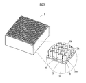
Figure 3 is a perspective view of an imaging element formed with the punch blades shown inFigure 2 ; -
Figure 4 is a microscope photograph of a manufactured imaging element; and -
Figure 5 is a microscope photograph of an imaging element in the case of applying no ultrasonic vibration. - With reference to
Figure 1 , a device configuration for manufacturing an imaging element is described as an embodiment of the present invention. The device for manufacturing an imaging element comprises anultrasonic welder 1 and ablade section 2 that is mounted on ahorn 11 of theultrasonic welder 1. - The
ultrasonic welder 1 comprises anultrasonic oscillation section 12 that applies ultrasonic vibration to thehorn 11, alifting section 13 that raises or lowers thehorn 11 and theultrasonic oscillation section 12 as a unit, a supportingsection 15 that supports thelifting section 13 at an adjustable height with acolumn 14, apedestal 16 that perpendicularly supports thecolumn 14 under thehorn 11, and acontroller 17 that controls actuations of theultrasonic oscillation section 12 and thelifting section 13. Thecontroller 17, theultrasonic oscillation section 12, and thelifting section 13 are connected with acable 18, through which signals are mutually transmitted. - The
ultrasonic oscillation section 12 comprises an internally disposed ultrasonic oscillator not shown in the drawing that receives control signals from thecontroller 17 to vibrate thehorn 11 at a predetermined oscillating frequency. - The
lifting section 13 comprises a servomotor and a ball screw connected to the main shaft (rotor) not shown in the drawing. By screwing the ball screw into a female screw disposed on the frame of theultrasonic oscillation section 12, theultrasonic oscillation section 12 is raised or lowered with the servomotor. - The supporting
section 15 comprises aside frame 15a that is connected to thelifting section 13 and alocking screw 15b that fixes theside frame 15a on thecolumn 14, so that the height positions of theside frame 15a and thelifting section 13 are adjustable using thelocking screw 15b. - The
pedestal 16 comprises a flat table 16a on the top, so that a substrate to be processed (work) 3 can be placed on the table 16a. - The
controller 17 comprises anoperation panel 17a and adisplay section 17b, so that the oscillating frequency of the ultrasonic oscillator in theultrasonic oscillation section 12 and the outputs of the servomotor in the lifting section 13 (rotating speed and torque) may be variably set through the manipulation of theoperation panel 17a by an operator. Control states and the like of theultrasonic oscillation section 12 and thelifting section 13 are displayed on thedisplay section 17b. - As shown in
Figure 2 , theblade section 2 comprisespunch blades 22 arranged in grid pattern on a surface of a thick plate-like metal block 21. The backside of themetal block 21 is fixed on thehorn 11 with means for fixing not shown in the drawing. - The shape of the
punch blade 22 is a four-sided pyramid having no top. Among the four sides, two neighboringsides metal block 21 and the angle between the twosides sides tip 22c of thepunch blade 22. Acounterbored portion 22d is formed by arc-circularly counterboring along thesides tip 22c. - In an embodiment of the present invention, the
punch blade 22 has a side length of 100 µm, and thepunch blades 22 are arranged lengthwise and crosswise on themetal block 21 allowing a 100-µm spacing between the neighboring blades. - In an embodiment of the present invention, the
punch blade 22 was formed by cutting the surface of themetal block 21 with a bite. Alternatively, thepunch blade 22 may be formed with a wire-electrical discharge machine or by polishing using a grinding stone. Material for themetal block 21 andpunch blades 22 is properly selected depending on the material of thesubstrate 3 to be processed. - Subsequently, a method for manufacturing an imaging element using the device configuration described above is described.
- Initially, two
substrates 3, each composed of a flat thin metal plate, are stacked and placed on the table 16a for fixing thereon. Thesubstrate 3 is a thin plate comprising one metal selected from, for example, aluminum, stainless steel, chromium, and molybdenum or an alloy of the two or more metals selected from these metals. These metals or alloys are suitable for processing with a punch and the punched surface (processed surface) has a high reflectance. - Although two
substrates 3 are stacked for ensuring the positive punching of asubstrate 3 using thedownside substrate 3 as a setting board in the embodiment of the present invention, asingle substrate 3 may be placed on the table 16a. - Before or after placing the
substrate 3 on the table 16a, fixing of theblade section 2 on thehorn 11 is confirmed to complete the advance preparation. - Subsequently, the
ultrasonic welder 1 is activated for setting the oscillating frequency of the ultrasonic oscillator in theultrasonic oscillation section 12 and the output of the servomotor in thelifting section 13 through the manipulation of theoperation panel 17a. The oscillating frequency of the ultrasonic oscillator is properly set in a range of, for example, 15 kHz to 60 kHz depending on the material of thesubstrate 3. The output of the servomotor is set after specifying the contact position between thepunch blade 22 and thesubstrate 3 and the punching completion position through preliminary teaching, such that the traveling between the contact position and the punching completion position is performed at a suitable processing speed for punching depending on the material of thesubstrate 3. - Subsequently, the
ultrasonic oscillation section 12 and thelifting section 13 are activated under predetermined conditions to punch thesubstrate 3. Thepunch blades 22 are ultrasonic-vibrated at a predetermined oscillating frequency through thehorn 11 with theultrasonic oscillation section 12 during punching. Consequently, thepunch blades 22 exhibit high cutting performance during traveling from the contact position with thesubstrate 3 to the punching completion position due to a synergetic effect of the vibration and the frictional heat between the blade and thesubstrate 3 resulting from the vibration. - Thus, as shown in
Figure 3 , a plurality ofmicro holes 31 is formed in thesubstrate 3 corresponding to thepunch blades 22 inFigure 2 . The two neighboringinner sides micro hole 31 corresponding to the twosides punch blade 22 are mirror surfaces perpendicular to thesubstrate 3. Using metal as material for thesubstrate 3, the punched surface has a higher reflectance compared to the surface using the other material, and the inner mirror surfaces 31 a and 31b can be produced without applying a reflection coating. - As described above, according to the embodiment of the method for manufacturing an imaging element, the imaging element can be readily manufactured by punching and highly smoothed mirror surfaces precisely perpendicular to the surface of the substrate can be produced. As a result, an accurately processed imaging element can be readily manufactured for saving cost and time.
- Subsequently, an example of the imaging element that was manufactured according to an embodiment of the method for manufacturing an imaging element is described below.
-
Figure 4 is a microscope photograph of an imaging element that was manufactured by processing an aluminum thin plate having a thickness of 100 µm as thesubstrate 3 by the method (applying 40-kHz ultrasonic vibration). - As shown in the microscope photograph in
Figure 4 , the imaging element comprises square micro holes arranged lengthwise and crosswise corresponding to thepunch blades 22. Since the squares have uniform sides and angles, it is comprehensible that each of the micro holes having a shape corresponding to thepunch blade 22 has two neighboring inner surfaces that form mirror surfaces. Since a bright and clear image was actually produced using the imaging element shown inFigure 4 , it was proved that the micro holes have mirror surfaces with a high reflectance. - In contrast,
Figure 5 is a microscope photograph of an imagine element without application of ultrasonic vibration. In that case, the conditions except for the presence or absence of the application of ultrasonic vibration were the same as for the case inFigure 4 . - In the microscope photograph in
Figure 5 , the outlines of the micro holes are blurred. This indicates that the formed shapes of the micro holes do not correspond to thepunch blades 22. In that case, no image was produced. It is comprehensible that no mirror surfaces were formed in the micro holes. - Subsequently, an imaging element was manufactured by processing a polycarbonate thin plate having a thickness of 100 µm as the
substrate 3 by the method (applying 40-kHz ultrasonic vibration). In that case, uniformly arranged micro holes, each having a uniform shape, were formed in the sale way as for the case inFigure 4 . - However, in that case, although an image was formed using the manufactured imaging element, a problem was that the image was dark. For dealing with the problem, an aluminum vapor deposited film having a thickness of 500 Å was formed on the surface of the manufactured imagine element. As a result, a bright and clear image was produced. It was proved that the reflectance of the mirror surfaces can be enhanced by coating the formed minor surfaces in the micro holes with a reflective coat.
- Although an ultrasonic vibration of 40 kHz was applied in the example described above, it was confirmed that equivalent imaging elements can be manufactured using any frequency in a range from 15 kHz to 60 kHz.
- As described above, according to the embodiment of the method for manufacturing an imaging element, an accurately processed imaging element can be readily manufactured for saving cost and time.
- In the present embodiment, the
punch blades 22 were vibrated with theultrasonic oscillation section 12. Alternatively, the table 16a may be vibrated with an ultrasonic oscillator disposed in thepedestal 16. In that case also, cutting performance during punching is enhanced due to a synergetic effect of the vibration and the frictional heat between thesubstrate 3 and thepunch blades 22 resulting from the vibration, so that an accurately processed imaging element can be readily manufactured for saving cost and time.
Claims (5)
- A method for manufacturing an imaging element comprising a flat substrate with a plurality of vertical micro through-holes, each having two inner mirror surfaces perpendicularly arranged for bending a light beam passing through the hole such that a real image of an object or a projected image disposed in the space facing one side of the flat substrate is formed in a space facing the other side, comprising:pressing a blade section in which a plurality of projecting punch blades are arranged, each punch blade having at least two sides corresponding to the mirror surfaces, into contact with the substrate while ultrasonically vibrating the blade section; and punching the substrate with the punch blades.
- A method for manufacturing an imaging element comprising a flat substrate with a plurality of vertical micro through-holes, each having two inner mirror surfaces perpendicularly arranged for bending a light beam passing through the hole such that a real image of an object or a projected image disposed in the space facing one side of the flat substrate is formed in a space facing the other side, comprising:pressing a blade section in which a plurality of projecting punch blades are arranged, each punch blade having at least two sides corresponding to the mirror surfaces, into contact with the substrate while ultrasonically vibrating a pedestal with the substrate fixed thereon; and punching the substrate with the punch blades.
- The method for manufacturing an imaging element according to claim 1, wherein the substrate is a thin metal plate.
- The method for manufacturing an imaging element according to claim 3, wherein the thin metal plate comprises any one metal selected from aluminum, stainless steel, chromium, and molybdenum or an alloy of the two or more metals selected therefrom.
- The method for manufacturing an imaging element according to claim 1, further comprising the step of coating the mirror surfaces with a reflective coat after the substrate is punched with the punch blades, wherein the substrate is a thin resin plate.
Applications Claiming Priority (2)
| Application Number | Priority Date | Filing Date | Title |
|---|---|---|---|
| JP2008239255A JP5456290B2 (en) | 2008-09-18 | 2008-09-18 | Method for creating imaging element |
| PCT/JP2009/004639 WO2010032450A1 (en) | 2008-09-18 | 2009-09-16 | Method for manufacturing imaging element |
Publications (2)
| Publication Number | Publication Date |
|---|---|
| EP2328001A1 true EP2328001A1 (en) | 2011-06-01 |
| EP2328001A4 EP2328001A4 (en) | 2011-09-07 |
Family
ID=42039298
Family Applications (1)
| Application Number | Title | Priority Date | Filing Date |
|---|---|---|---|
| EP09814295A Withdrawn EP2328001A4 (en) | 2008-09-18 | 2009-09-16 | METHOD OF MANUFACTURING AN IMAGE ELEMENT |
Country Status (6)
| Country | Link |
|---|---|
| US (1) | US8584561B2 (en) |
| EP (1) | EP2328001A4 (en) |
| JP (1) | JP5456290B2 (en) |
| KR (1) | KR20110063674A (en) |
| CN (1) | CN102159973B (en) |
| WO (1) | WO2010032450A1 (en) |
Cited By (4)
| Publication number | Priority date | Publication date | Assignee | Title |
|---|---|---|---|---|
| CN103978084A (en) * | 2013-02-07 | 2014-08-13 | 日本发条株式会社 | Method of punching out a damper, punching apparatus and attaching apparatus |
| WO2016207524A1 (en) * | 2015-06-24 | 2016-12-29 | Gaztransport Et Technigaz | Method and device for cutting fibrous or cellular insulating material |
| WO2020118431A1 (en) | 2018-12-13 | 2020-06-18 | HYDRO-QUéBEC | Cutting soft metals with the aid of ultrasound |
| EP4219089A1 (en) * | 2022-01-28 | 2023-08-02 | Abb Schweiz Ag | A punching cell for punching workpieces |
Families Citing this family (10)
| Publication number | Priority date | Publication date | Assignee | Title |
|---|---|---|---|---|
| EP2612736B1 (en) * | 2012-01-04 | 2019-09-11 | Siemens Aktiengesellschaft | Cutting machine with variation of the cutting area |
| JP5996260B2 (en) * | 2012-05-09 | 2016-09-21 | 株式会社ディスコ | Workpiece division method |
| JP2014008585A (en) * | 2012-07-02 | 2014-01-20 | Nagamine Seisakusho:Kk | Porous plate manufacturing tool, method of manufacturing porous plate, and porous plate |
| JP2017131397A (en) * | 2016-01-27 | 2017-08-03 | 花王株式会社 | Manufacturing method of fine hollow protrusion |
| US10987745B2 (en) | 2019-01-25 | 2021-04-27 | Snap-On Incorporated | Method of manufacturing socket punches |
| KR102291288B1 (en) * | 2019-05-21 | 2021-08-20 | 한국세라믹기술원 | Patterning Complex Device and operating method of the same |
| CN110509349B (en) * | 2019-08-27 | 2021-02-19 | 苏州骏创汽车科技股份有限公司 | Punching device for automotive plastic interior trim injection molding part |
| US11897074B2 (en) * | 2020-02-20 | 2024-02-13 | The Boeing Company | Needle arrays for forming ultrasonic perforations, and methods of making the same |
| US12330258B2 (en) | 2020-02-20 | 2025-06-17 | The Boeing Company | Methods of ultrasonic drilling for forming perforations in composite materials |
| CN114872132B (en) * | 2022-05-07 | 2023-03-24 | 中国民用航空飞行学院 | Hole opening device for thermoplastic sheet |
Family Cites Families (7)
| Publication number | Priority date | Publication date | Assignee | Title |
|---|---|---|---|---|
| US3756880A (en) * | 1971-03-19 | 1973-09-04 | Eastman Kodak Co | Moval ultrasonic perforating a sheet of film paper or the like with chip re |
| JPH08132396A (en) * | 1994-11-08 | 1996-05-28 | Murata Mfg Co Ltd | Punching method for soft sheet member, and punching device for soft sheet member |
| JPH10193299A (en) * | 1996-12-27 | 1998-07-28 | Ricoh Co Ltd | Manufacturing method of micro-hole forming die and micro-hole forming apparatus |
| FR2786714A1 (en) * | 1998-12-07 | 2000-06-09 | Vivier Harry J P | Method for producing micro-bores in metal work-piece involves forming hardened points on plate which is used as punch for sheet metal work-piece placed in die |
| JP2000326144A (en) * | 1999-04-12 | 2000-11-28 | Cts Corp | Porous micropunching equipment and manufacture therefor |
| US20070069003A1 (en) * | 2003-10-22 | 2007-03-29 | Teruie Takemasu | Boring device and boring method |
| US8057043B2 (en) * | 2006-03-23 | 2011-11-15 | National Institute Of Information And Communications Technology | Imaging element and display with micro mirror array |
-
2008
- 2008-09-18 JP JP2008239255A patent/JP5456290B2/en not_active Expired - Fee Related
-
2009
- 2009-09-16 US US13/119,477 patent/US8584561B2/en not_active Expired - Fee Related
- 2009-09-16 EP EP09814295A patent/EP2328001A4/en not_active Withdrawn
- 2009-09-16 WO PCT/JP2009/004639 patent/WO2010032450A1/en not_active Ceased
- 2009-09-16 CN CN2009801367532A patent/CN102159973B/en not_active Expired - Fee Related
- 2009-09-16 KR KR1020117008758A patent/KR20110063674A/en not_active Ceased
Cited By (8)
| Publication number | Priority date | Publication date | Assignee | Title |
|---|---|---|---|---|
| CN103978084A (en) * | 2013-02-07 | 2014-08-13 | 日本发条株式会社 | Method of punching out a damper, punching apparatus and attaching apparatus |
| CN103978084B (en) * | 2013-02-07 | 2016-09-28 | 日本发条株式会社 | The method stamping out vibroshock, pressing equipment and attached peripheral device |
| WO2016207524A1 (en) * | 2015-06-24 | 2016-12-29 | Gaztransport Et Technigaz | Method and device for cutting fibrous or cellular insulating material |
| FR3037843A1 (en) * | 2015-06-24 | 2016-12-30 | Gaztransport Et Technigaz | METHOD AND DEVICE FOR CUTTING FIBROUS OR ALVEOLA INSULATING MATERIAL |
| CN107921654A (en) * | 2015-06-24 | 2018-04-17 | 气体运输技术公司 | A kind of method and device for cutting fibre or porous heat insulation material |
| WO2020118431A1 (en) | 2018-12-13 | 2020-06-18 | HYDRO-QUéBEC | Cutting soft metals with the aid of ultrasound |
| EP3894152A4 (en) * | 2018-12-13 | 2022-08-17 | Hydro-Québec | SOFT METAL CUTTING BY ULTRASOUND ASSISTANCE |
| EP4219089A1 (en) * | 2022-01-28 | 2023-08-02 | Abb Schweiz Ag | A punching cell for punching workpieces |
Also Published As
| Publication number | Publication date |
|---|---|
| US20110162495A1 (en) | 2011-07-07 |
| EP2328001A4 (en) | 2011-09-07 |
| US8584561B2 (en) | 2013-11-19 |
| JP5456290B2 (en) | 2014-03-26 |
| WO2010032450A1 (en) | 2010-03-25 |
| KR20110063674A (en) | 2011-06-13 |
| JP2010072306A (en) | 2010-04-02 |
| CN102159973B (en) | 2013-04-24 |
| CN102159973A (en) | 2011-08-17 |
Similar Documents
| Publication | Publication Date | Title |
|---|---|---|
| US8584561B2 (en) | Method for manufacturing imaging element | |
| KR101286821B1 (en) | Ultrasonic bonding tool, method for manufacturing ultrasonic bonding tool, ultrasonic bonding method, and ultrasonic bonding apparatus | |
| JP2014217941A (en) | Cutting method and cutting device | |
| JP4251203B2 (en) | Method for scribing bonded mother substrate and dividing method for bonded mother substrate | |
| KR102259441B1 (en) | Breaking apparatus and dividing method | |
| CN104507884A (en) | Scribing wheels with precision structured grooves | |
| CN107240574A (en) | Substrate segmenting device | |
| KR20120087920A (en) | Method for breaking brittle material substrate | |
| TWI620634B (en) | Expander, breaking device and breaking method | |
| TWI735719B (en) | Glass plate and manufacturing method of glass plate | |
| EP2033781A1 (en) | Squeegee for printing device, printing device, and printing method | |
| WO2010070993A1 (en) | Substrate cleaning apparatus | |
| JP2002283225A (en) | Machining device and machining method of concave spherical surface | |
| WO2018161570A1 (en) | Carrying platform, cutting method therefor and processing device | |
| KR102027136B1 (en) | Scribing apparatus | |
| KR100919469B1 (en) | Ripping process of precision cutting blade | |
| JP2023115709A (en) | adhesive structure | |
| WO2000059725A1 (en) | Method and apparatus for stamping a part from a multi-layered strip | |
| KR20100045135A (en) | Substrate scribing apparatus and method of scribing substrate using the same | |
| JP3803731B2 (en) | Reflector, method for manufacturing reflector, and tool for plastic deformation thereof | |
| JP2012161843A (en) | Method for forming opening on substrate | |
| JP4513647B2 (en) | Optical element manufacturing method | |
| JP2024008133A (en) | Electronic component manufacturing method and electronic component manufacturing device | |
| WO2023153061A1 (en) | Adhesive structure | |
| JP2003048196A (en) | Method of cutting substrate, and device using the method |
Legal Events
| Date | Code | Title | Description |
|---|---|---|---|
| PUAI | Public reference made under article 153(3) epc to a published international application that has entered the european phase |
Free format text: ORIGINAL CODE: 0009012 |
|
| 17P | Request for examination filed |
Effective date: 20110318 |
|
| AK | Designated contracting states |
Kind code of ref document: A1 Designated state(s): AT BE BG CH CY CZ DE DK EE ES FI FR GB GR HR HU IE IS IT LI LT LU LV MC MK MT NL NO PL PT RO SE SI SK SM TR |
|
| AX | Request for extension of the european patent |
Extension state: AL BA RS |
|
| A4 | Supplementary search report drawn up and despatched |
Effective date: 20110809 |
|
| RIC1 | Information provided on ipc code assigned before grant |
Ipc: B21D 28/34 20060101ALI20110803BHEP Ipc: B21D 28/26 20060101ALI20110803BHEP Ipc: B26F 1/14 20060101ALI20110803BHEP Ipc: B26D 7/08 20060101ALI20110803BHEP Ipc: G02B 5/08 20060101AFI20110803BHEP |
|
| DAX | Request for extension of the european patent (deleted) | ||
| STAA | Information on the status of an ep patent application or granted ep patent |
Free format text: STATUS: THE APPLICATION IS DEEMED TO BE WITHDRAWN |
|
| 18D | Application deemed to be withdrawn |
Effective date: 20120306 |