EP2326014A2 - Error detecting/correcting code generating circuit and method of controlling the same - Google Patents
Error detecting/correcting code generating circuit and method of controlling the same Download PDFInfo
- Publication number
- EP2326014A2 EP2326014A2 EP10189814A EP10189814A EP2326014A2 EP 2326014 A2 EP2326014 A2 EP 2326014A2 EP 10189814 A EP10189814 A EP 10189814A EP 10189814 A EP10189814 A EP 10189814A EP 2326014 A2 EP2326014 A2 EP 2326014A2
- Authority
- EP
- European Patent Office
- Prior art keywords
- bits
- error
- code
- bit
- detection
- Prior art date
- Legal status (The legal status is an assumption and is not a legal conclusion. Google has not performed a legal analysis and makes no representation as to the accuracy of the status listed.)
- Granted
Links
Images







Classifications
-
- H—ELECTRICITY
- H03—ELECTRONIC CIRCUITRY
- H03M—CODING; DECODING; CODE CONVERSION IN GENERAL
- H03M13/00—Coding, decoding or code conversion, for error detection or error correction; Coding theory basic assumptions; Coding bounds; Error probability evaluation methods; Channel models; Simulation or testing of codes
- H03M13/03—Error detection or forward error correction by redundancy in data representation, i.e. code words containing more digits than the source words
- H03M13/05—Error detection or forward error correction by redundancy in data representation, i.e. code words containing more digits than the source words using block codes, i.e. a predetermined number of check bits joined to a predetermined number of information bits
- H03M13/13—Linear codes
- H03M13/19—Single error correction without using particular properties of the cyclic codes, e.g. Hamming codes, extended or generalised Hamming codes
-
- H—ELECTRICITY
- H03—ELECTRONIC CIRCUITRY
- H03M—CODING; DECODING; CODE CONVERSION IN GENERAL
- H03M13/00—Coding, decoding or code conversion, for error detection or error correction; Coding theory basic assumptions; Coding bounds; Error probability evaluation methods; Channel models; Simulation or testing of codes
- H03M13/03—Error detection or forward error correction by redundancy in data representation, i.e. code words containing more digits than the source words
- H03M13/033—Theoretical methods to calculate these checking codes
-
- H—ELECTRICITY
- H03—ELECTRONIC CIRCUITRY
- H03M—CODING; DECODING; CODE CONVERSION IN GENERAL
- H03M13/00—Coding, decoding or code conversion, for error detection or error correction; Coding theory basic assumptions; Coding bounds; Error probability evaluation methods; Channel models; Simulation or testing of codes
- H03M13/61—Aspects and characteristics of methods and arrangements for error correction or error detection, not provided for otherwise
- H03M13/618—Shortening and extension of codes
-
- H—ELECTRICITY
- H03—ELECTRONIC CIRCUITRY
- H03M—CODING; DECODING; CODE CONVERSION IN GENERAL
- H03M13/00—Coding, decoding or code conversion, for error detection or error correction; Coding theory basic assumptions; Coding bounds; Error probability evaluation methods; Channel models; Simulation or testing of codes
- H03M13/65—Purpose and implementation aspects
- H03M13/6575—Implementations based on combinatorial logic, e.g. Boolean circuits
Definitions
- the present invention relates to an error detecting/correcting code generating circuit and a method of controlling the error detecting/correcting code generating circuit.
- Japanese Laid-Open Patent Publication No. 6-324951 discusses an error correcting code function and a parity interface scheme providing a translation capability between the error correcting code and parity protocols that are implemented for memory systems in personal computers.
- Japanese Laid-Open Patent Publication No. 48-66334 discusses a parity check circuit for a data transfer system in which information is exchanged between a data processing unit and a memory unit having an ECC (Error Checking and Correction) code.
- the parity check circuit includes a code converting unit that performs code conversion between the ECC code and the parity check bit. It is discussed that the parity check bit can be directly calculated by an operating unit.
- the present disclosure aims at providing an error detecting/correcting code generating circuit capable of generating an error detecting/correcting code using a simple structure, and a method of controlling the error detecting/correcting code generating circuit.
- the invention may provide an error detecting/correcting code generating circuit including a first Exclusive-OR operation circuit that generates log 2 (n+1) bits of one portion of a redundant portion of error detecting/correcting-code-attached data by rounding up the numbers to the right of the decimal point of log 2 (n+1) in response to the input of m bytes of an information portion included in error-detection-bit-attached data.
- the error-detection-bit-attached data includes a redundant portion of m bits of error detection bits allocated to the m bytes of the information portion, the byte having n bits.
- the circuit also includes a second Exclusive-OR operation circuit that generates m bits of another portion of the redundant portion of the error detecting/correcting-code-attached data in response to the input of the one portion and the error detection bits.
- the invention may provide a method of controlling an error detecting/correcting code generating circuit, the method including generating one portion of log 2 (n+l) bits of a redundant portion of error detecting/correcting-code-attached data by rounding up the numbers to the right of the decimal point of log 2 (n+l) in response to the input of m bytes of an information portion included in error-detection-bit-attached data, using a first Exclusive-OR operation circuit of the error detecting/correcting code generating circuit.
- the error-detection-bit-attached data includes a redundant portion of m bits of error detection bits allocated to the m bytes of the information portion, each byte having n bits.
- the method also includes generating another portion of m bits of the redundant portion of the error detecting-code-attached data in response to the input of the log 2 (n+1) bits of the one portion and the error detection bits, using a second Exclusive-OR operation circuit of the error detecting/correcting code generating circuit.
- the invention may provide a data operating unit including a memory in which error detecting/correcting-code-attached data including an information portion of m bytes and a redundant portion is written, each byte having n bits; and an error detecting/correcting code generating circuit including a first Exclusive-OR operation circuit and a second Exclusive-OR operation circuit.
- the first Exclusive-OR operation circuit generates one portion of log 2 (n+1) bits of the redundant portion of the error detecting/correcting-code-attached data by rounding up the numbers to the right of the decimal point of log 2 (n+l), in response to the input of the m bytes of the information portion included in error-detection-bit-attached data.
- the error-detection-bit-attached data includes a redundant portion of m bits of error detection bits allocated to the m bytes of the information portion.
- the second Exclusive-OR operation circuit generates another portion of m bits of the redundant portion of the error detecting/correcting-code-attached data in response to the input of the one portion and the error detection bits.
- the unit also includes an error detecting/correcting circuit that detects or corrects an error in the information portion in response to the input of the redundant portion of the error detecting/correcting-code-attached data read from the memory; an error-detection-bit-attached data generating circuit that generates the error-detection-bit-attached data having the m bytes of the information portion of the error detecting/correcting-code-attached data read from the memory and the redundant portion having the bits of the error detection bits allocated to the m bytes of the information portion; and an operating unit that performs an operating process on the error-detection-bit-attached data.
- the invention may provide a data operating unit including a memory in which error detecting/correcting-code-attached data of (n+ 1 )m+[log 2 (n+l)] bits including an information portion of mn bits and a redundant portion are written.
- the redundant portion includes one portion of [log 2 (n+1)] bits and another portion of m bits, [log 2 (n+1)] indicating log 2 (n+1) from which the numbers to the right of the decimal point have been rounded up.
- the unit also includes an error-detection-bit-attached data generating circuit that generates each bit of a redundant portion of error-detection-bit-attached data by using a maximum of [log 2 (n+1)] bits of the redundant portion of the error detecting/correcting-code-attached data read from the memory.
- the error detecting/correcting-code-attached data includes the information portion.
- the redundant portion of the error detecting/correcting-code-attached data includes error detection bits of which one bit is allocated to every n bits of the information portion.
- the unit also includes an error detecting/correcting circuit that detects or corrects an error in the information portion in response to the input of the redundant portion of the error detecting/correcting-code-attached data read from the memory; and an operating unit that performs an operating process on the error-detection-bit-attached data.
- FIG. 1 illustrates a circuit for generating a redundant portion of the SECDED code according to a related technology
- Fig- 2 illustrates a circuit for generating a redundant portion of the SECDED code according to an embodiment of the present invention
- FIG. 3 illustrates a circuit for generating a redundant portion of a byte parity code
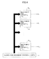
- FIG. 4 illustrates a circuit for generating a redundant portion of the byte parity code according to an embodiment of the present invention
- FIG. 5 illustrates a specific example of the circuit structure illustrated in FIG. 1 ;
- FIG. 6 illustrates a first example of the circuit structure illustrated in FIG. 2 ;
- FIG. 7 illustrates a second example of the circuit structure illustrated in FIG. 2 ;
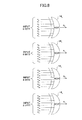
- FIG. 8 illustrates a specific example of the circuit structure illustrated in FIG. 3 ;
- FIG. 9 illustrates a first example of the circuit structure illustrated in FIG. 4 ;
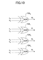
- FIG. 10 illustrates a second example of the circuit structure illustrated in FIG. 4 ;
- FIG. 11 is a block diagram of a data operating unit according to an embodiment of the present invention.
- FIG. 12 is a block diagram of the data operating unit according to another embodiment of the present invention.
- An Exclusive-OR (hereafter "XOR") circuit tree may generate a parity bit and an ECC (Error Checking and Correction) checking bit in response to the input of data.
- the XOR circuit tree may have data inputs A through P of which data inputs A through H are involved in the generation of the ECC checking bit and the parity bit, while data inputs I through P are only involved in the generation of the ECC checking bit.
- the parity bit in whose generation data inputs A through H are involved and the ECC checking bit in whose generation data inputs I through P are involved may be involved in the generation of an ECC checking bit for data inputs A through P.
- a code conversion method may involve calculating a parity bit based on a data bit and an error correcting code attached to the data bit.
- [log2 (n+1)] is a natural number such that log 2 (n+1) ⁇ [log 2 (n+1)] ⁇ log 2 (n+1)+1, i.e., a number obtained by rounding up the numbers to the right of the decimal point of log 2 (n+1).
- the SECDED code ⁇ includes the nm bits of the information portion and the m bits of the redundant portion of data ⁇ , and the [log 2 (n+1)] bits of the other redundant portion, for a total of (n+1)m+[log 2 (n+1)] bits.
- An electronic circuit may include an error detecting/correcting circuit, such as a RAS (Reliability, Availability and Serviceability) circuit.
- the RAS circuit may be used for detecting a built-in defect introduced during a manufacturing process, or detecting and correcting a data error caused by voltage variation or ⁇ rays or neutron rays and the like during the use of the product.
- RAS Reliability, Availability and Serviceability
- the RAS circuit may be used for detecting a built-in defect introduced during a manufacturing process, or detecting and correcting a data error caused by voltage variation or ⁇ rays or neutron rays and the like during the use of the product.
- redundancy in the data as the subject of error detection or correction, in addition to providing the RAS circuit as a hardware component.
- the size of a redundant portion of the data may vary depending on the purpose of the error detection or correction.
- a method may involve allocating one bit of a parity bit for every 8 bits of information (data), the parity bit being logically equal to a value obtained by an XOR operation of the information 8 bits, and providing a circuit for calculating an XOR operation of the 8 bits of information and the parity bit in order to detect a single-bit error.
- This method is often used in cases where the frequency of error in the information is not so high and there is no tendency of multiple bits of error occurring in adjacent bits of the information, and when the RAS circuit cannot be provided with sufficient resources or execution latency.
- the method may be used within an operating unit of a processor.
- the data in which a parity bit (redundant portion) is attached to information (information portion) so that a single-bit error in the information can be detected as described above is referred to as a "byte parity code" .
- a RAS circuit capable of not just detection but correction of an error is often employed. For example, by adding 7 bits of redundant bits to 32 bits of data (for a total of 39 bits), an error correcting code (ECC) capable of single-bit error correction and double-bit error detection can be generated.
- ECC error correcting code
- SECDED Single bit Error Correct and Double bit Error Detect
- the SECDED code may include an "extended Hamming code" which is a Hamming code capable of single-bit error correction to which one bit generated from an XOR operation of the entire data is added.
- extended Hamming code is a Hamming code capable of single-bit error correction to which one bit generated from an XOR operation of the entire data is added.
- the RAS circuit may be variously configured to suit the particular purpose, so that the data having the same information content may have different forms depending on the type of the RAS circuit.
- transmission of data from RAM to an operating unit may involve conversion from the SECDED code to the byte parity code.
- transmission of data from the operating unit to RAM may involve conversion of the data from the byte parity code to the SECDED code.
- the relevant technology may directly generate the redundant portion of the byte parity code or the SECDED code by utilizing the information portion.
- the redundant portion of the byte parity code may be generated by an XOR operation of 8 bits of the information portion, or the redundant portion of 32 bits of data of a SECDED code may be generated by an XOR operation of some of the 32 bits of the information portion.
- the relevant technology rarely generates a code by utilizing the code of the other party.
- the redundant portions of different codes can be mutually utilized for generating each other's codes, the amount of circuitry necessary for generating codes may be reduced and also execution latency may be reduced.
- the number of circuits necessary for code generation and execution latency are reduced by mutually utilizing the redundant portions of the byte parity code and the SECDED code when mutual conversion is performed between them.
- the SECDED code is generated in such a manner that enables the relevance between the redundant portions of the byte parity code and the SECDED code to be readily found in order to facilitate mutual utilization.
- the redundant portion of the SECDED code by utilizing the parity bit (i.e., the redundant portion of the byte parity code) of which one bit is added to n bits of information.
- the number of gates in the RAS circuit can be reduced, the speed of the RAS circuit can be increased (i.e., delay can be reduced), and the ease and coverage of logic inspection of the RAS circuit can be enhanced.
- data byte parity code
- B indicates the d-order column vector where (i ⁇ j) for given O ⁇ i, j ⁇ n, and b( i ) and b(j)(i ⁇ j) are mutually linearly independent.
- C ⁇ d bit c 0 c 1 c 2 ... c d - 2 c d - 1 ⁇ m bit
- C indicates an m-order column vector where (i ⁇ j) for given 0 ⁇ i., j ⁇ n and C (i) and c(j) (i ⁇ j) are mutually linearly independent.
- the number of times that "1" appears in each column vector C(i) of the matrix C is an odd number.
- the matrixes B and C may be made by more than one way.
- a generating matrix for generating the SECDED code may be made based on the check matrix H.
- the check matrix H When three column vectors are arbitrarily selected from the check matrix H, those three column vectors are mutually linearly independent, as will be described later. This is a condition for the check matrix H to be a check matrix for the SECDED code.
- p i v i 0 + v i 1 + ... + v i ⁇ n - 2 + v i n - 1
- the check matrix H satisfies the a forementioned condition for it to be a check matrix for the SECDED code.
- the check matrix H satisfies the aforementioned condition for it to be a check matrix for the SECDED code. How the two check matrixes (1) and (2) are selected is described later.
- a vector in a field F 2 in which N bits of the information portion are laterally arranged is considered.
- the information portion includes m bytes (each byte having n bits), as mentioned above.
- the result of calculation of the left-hand side of equation (3) indicates a value other than "0".
- the calculation result of the left-hand side of equation (3) i.e., a column vector
- the error bit A bit in the information portion v included in the element vc of the SECDED code that corresponds to the position of the coinciding column vector in the check matrix H is the error bit.
- the error bit can be corrected.
- the column vector as a result of the calculation of the left-hand side of equation (3) is a value other than "0", as in the case of the single-bit error.
- the calculation result is a column vector of which the number of 1's included in the upper m bits is an even number (including zero).
- the "upper m bits” may refer to the upper four bits of each column vector included in the check matrix H according to equation (1) or (2).
- the SECDED code generated based on the check matrix H according to the present embodiment of the present invention, a single-bit error of the information portion v of the SECDED code can be corrected and a double-bit error can be detected.
- the SECDED code according to the present embodiment can provide proper functions of the SECDED code.
- Equation (4) of expression 21 is a formula for obtaining the redundant portion of the SECDED code according to the present embodiment, where the redundant portion is determined by the shape of the column vector.
- the lower d bits (C 2 t ) of the column vector are generated from the sum of some of the components of the information portion v, and that the upper m bits (i.e., c 1 t ) are generated by the sum of some of the components of the lower d bits ( C2 t ) of the generated redundant portion and a single parity bit p t .
- a single conversion circuit using the matrix B for v i - 1 t may be realized that calculates C 2 t by repeating the cycle of adding B.v i-1 t obtained by the conversion circuit while updating i.
- the size of the circuit for generating C 2 t may be reduced to approximately 1/m of the normal size.
- a circuit that directly obtains the polynomial B ⁇ v 0 t + B.v 1 t + ... + B ⁇ v m-1 t included in equation (4) may be provided. Further, the above two types of circuits may be combined into a hybrid circuit.
- Equation (5) of expression 22 is a formula for determining the redundant portion of the byte parity code according to the present embodiment. According to equation (5), the parity bit can be generated only from the redundant portions c 1 and C2 of the SECDED code.
- the matrix C may be selected such that "1" appears only once in the components of each column vector.
- the matrix Cony needs to be a. permutation matrix (including a unit matrix).
- An example is the matrix C of expression 9 used in the check matrix H (2) of expressions 9 and 10. The number of terms required in this case is two (see equation (2-2) of expression 31 as will be described later).
- all of the parity bits can be generated by simply calculating the sum of one each of the components c 2 t and C2 t (i.e., XOR operation).
- This example is very effective when data stored in memory in the SECDED code format is read by converting the data into byte-parity-code format data.
- the circuit for such data conversion requires only one 2-input XOR circuit for each bit of the parity bits (see FIG. 10 which will be described later).
- each of the lower 4 bits (C 4 ,...,C 7 ) of the redundant portion can be generated by performing four cycles of summing of three terms.
- the size of the circuit for generating the SECDED code can be further reduced, and the required operations can be simplified.
- the SECDED code of 32 bit data is generated by using a check matrix of the SECDED code according to the relevant technology.
- the check matrix may be selected such that the number of times of addition during code generation can be minimized.
- row 1 of the matrix on the right-hand side of expression 26 is obtained as the sum of the bits of the information portion v corresponding to "1" in the 32 bits in row 1 of the check matrix.
- the maximum number of terms added is 15 (c 6 ) and the minimum number is 11 (c 3 ).
- the present embodiment requires less calculation for generating the redundant potion of the SECDED code than the relevant technology.
- the present embodiment is superior to the relevant technology from the viewpoint of the size of the circuit for generating the redundant portion of the SECDED code, and freedom of designing the circuit.
- the present embodiment is also superior to the relevant technology from the viewpoint of delay (latency) of the operating process.
- the number of terms required for generating each of the parity bits is 8, i.e., twice as many as in the case of the present embodiment illustrated by expression 27.
- the present embodiment is also superior to the relevant technology from the viewpoint of required circuit size as regards the generation of the byte parity code, for example.
- equation (4) of expression 21 derived from the respective elements within the check matrix H according to expression 1 for the SECDED code according to the present embodiment the matrix B appears repeatedly.
- a small-sized logic module can be repeatedly used in a logic process for generating the redundant portion of the SECDED code.
- a logic verifying process may be performed on the small-sized module unit basis.
- the circuit for generating the redundant portion of the SECDED code does not have any specific regularity, so that the logic verifying process has to be performed on the entire check matrix.
- a logic verifying process for the logic circuit can be simplified compared with the relevant technology, so that verification coverage improves.
- the check matrix used may be selected depending on the purpose.
- the check matrix (1) may be used when it is desired to simplify the logic for generating the redundant portion of the SECDED code, while using the check matrix (2) when it is desired to simplify the logic for generating the redundant portion of the byte parity code.
- FIG. 1 illustrates a circuit for generating the redundant portion of the SECDED code according to the relevant technology.
- the circuit is configured to realize the logic of expression 32.
- "G" in the right-hand side member of expression 32 indicates a generating matrix used for generating the redundant portion of the SECDED code.
- FIG. 2 illustrates a circuit for generating the redundant portion of the SECDED code according to the present embodiment.
- the circuit realizes the logic according to expressions 33 and 34.
- B d v 0 + B d v 1 + ... + B d ⁇ v m - 1 B ⁇ v 0 t
- Expression 33 corresponds to the upper m bits of equation (4) of expression 21.
- Expression 34 corresponds to the lower d bits of equation (4) of expression 21.
- "C" in the right-hand side member of expression 33 indicates the matrix C defined in the definition of the check matrix H according to expression 6.
- each Bi(v j ), namely each Bi in FIG. 2 is a function to which v j is inputted, namely a multiple-input XOR circuit to which some of the components of the vector v j are inputted.
- "B" in the right-hand side member of expression 34 indicates the matrix B defined in the definition of the check matrix H of expression 5.
- FIG. 3 illustrates a circuit for generating the redundant portion of the byte parity code according to the relevant technology.
- p i v i 0 + v i 1 + ... + v i ⁇ n - 2 + v i ⁇ n - 1
- FIG. 4 illustrates a circuit for generating the redundant portion of the byte parity code according to the present embodiment.
- the circuit realizes the logic according to expression 36.
- "C" in the right-hand side member of expression 36 indicates the matrix C defined in the definition of the check matrix H according to expression 6.
- FIG. 5 illustrates a concrete example of the circuit structure illustrated in FIG. 1 .
- the example includes seven XOR circuits 11 0 ,...,11 6 and is configured to realize the logic according to expression 26.
- FIG. 6 illustrates a first example of the circuit structure illustrated in FIG. 2 .
- the first example is a conversion circuit (corresponding to the ECC generating circuit 2 illustrated in FIGs. 11 and 12 ) that generates the SECDED code from the byte parity code.
- the conversion circuit illustrated in FIG. 6 is based on the check matrix H expressed by equation (1) of expression 8, and it realizes the logic according to equations (1-1) and (1-2) of expression 24.
- the four XOR circuits 13 0 ,...,13 3 are configured to generate the upper m bits (c 0 ,...,c 3 ) of the redundant portion of the SECDED code, while the other four XOR circuits 12 4 ,...,12 7 are configured to generate the lower d bits (c 4 ,...,c 7 ) of the redundant portion of the SECDED code.
- the lower d bits (c 4 ,...,c 7 ) of the redundant portion of the SECDED code ß are generated based on the information portion v of the byte parity code ⁇ .
- FIG. 7 illustrates a second example of the circuit structure illustrated in FIG. 2 .
- the second example is a conversion circuit (ECC generating circuit 2 in FIGs. 11 and 12 ) that generates the SECDED code from the byte parity code according to the present embodiment of the present invention.
- the circuit of FIG. 7 is based on the check matrix H expressed by equation (2) of expression 10 and configured to realize the logic according to equation (2-1) of expression 30.
- equation (2) of expression 10 expressed by equation (2) of expression 10 and configured to realize the logic according to equation (2-1) of expression 30.
- the four XOR circuits 13A 0 ,...,13A 3 are configured to generate the upper m bits (C 0 ,...,C 3 ) of the redundant portion of the SECDED code
- the other four XOR circuits 12A 4 ,...,12A 7 are configured to generate the lower d bits (C 4 ,...,C 7 ) of the redundant portion of the SECDED code.
- c 0 ,...,p 3 the parity bits (p 0 ,...,p 3 ) of the byte parity code ⁇
- FIG. 8 illustrates a specific example of the circuit structure depicted in FIG. 3 .
- the example is configured to generate the byte parity code by the relevant technology.
- the circuit includes four XORs 14 0 ,...,14 3 and is configured to realize the logic according to expression 28.
- FIG. 9 illustrates a first example of the circuit structure illustrated in FIG. 4 .
- the example is a conversion circuit (corresponding to the parity generating circuit 5 in FIGs. 11 and 12 ) for generating the byte parity code from the SECDED code according to the present embodiment.
- the circuit of FIG. 9 is based on the check matrix H expressed by equation (1) of expression 8, and is configured to realize the logic of equation (1-3) of expression 27 by using four XORs 15 0 ,...,15 3 .
- FIG. 10 illustrates a second example of the circuit structure depicted in FIG. 4 .
- the example is a conversion circuit (parity generating circuit 5 in FIGs. 11 and 12 ) that generates the byte parity code from the SECDED code according to the present embodiment.
- the circuit of FIG. 10 is based on the check matrix H expressed by equation (2) of expression 10, and is configured to realize the logic of equation (2-2) of expression 31 by using four XORs 15A 0 ,...,15A 3 .
- FIG. 11 is a block diagram of a data operating unit according to an embodiment of the present invention.
- the data operating unit includes an operating unit 1, an ECC generating circuit 2, a memory 3, an error detecting/correcting circuit 4, and a parity generating circuit 5.
- the memory 3 stores data of the SECDED code format according to the foregoing embodiments.
- the operating unit 1 reads the data from the memory 3 and executes an operating process on the data.
- the error detecting/correcting circuit 4 first performs an error detecting/correcting process on the data.
- the error detecting/correcting circuit 4 which may include the RAS circuit, detects an error in the information portion of the SECDED code by using the redundant portion of the SECDED code read from the memory 3.
- the SECDED code is configured to enable detection and correction of a single-bit error and detection of a double-bit error. Therefore, the error detecting/correcting circuit 4 can detect and correct a single-bit error and detect a double-bit error in the information portion of the SECDED code.
- the error detecting/correcting circuit 4 delivers the SECDED code to the parity generating circuit 5. When correcting a bit error, the error detecting/correcting circuit 4 may overwrite a corrected bit in the memory 3.
- the parity generating circuit 5 converts the SECDED code provided by the error detecting/correcting circuit 4 into the byte parity code, and sends the byte parity code to the operating unit 1.
- the parity generating circuit 5 may have a structure illustrated in FIG. 4 .
- the parity generating circuit 5 based on the redundant portion of the SECDED code, generates the parity bits p 0 ,...,p m-1 of the redundant portion of the byte parity code, using the XOR circuits 15 0 ,...,15 m-1 .
- the parity generating circuit 5 then attaches the parity bits to the information portion of the SECDED code, thereby obtaining the byte parity code which is sent to the operating unit 1.
- the operating unit 1 executes an operating process on the byte parity code sent from the parity generating circuit 5, and hands the processed byte parity code to the ECC generating circuit 2.
- the ECC generating circuit 2 converts the byte parity code into the SECDED code and writes the SECDED code in the memory 3.
- the ECC generating circuit 2 may have a structure illustrated in FIG. 2 .
- the ECC generating circuit 2 based on the information portion v of the byte parity code, generates the lower d bits (C m ,...,C k-1 ) of the redundant portion of the SECDED code by using the XOR circuits 12 m ,...,12 k-1 .
- the ECC generating circuit 2 based on the lower d bits (c m ,...,c k-1 ) of the redundant portion of the SECDED code and the parity bits (p 0 ,...,p m - 1 ) of the byte parity code, generates the upper m bits (c 1 ,...,c m-1 ) of the redundant portion of the SECDED code by using the XOR circuits 13 0 ,...,13 m-1 . Then, the ECC generating circuit 2 attaches the lower d bits and the upper m bits of the redundant portion of the SECDED code to the information portion of the byte parity code, thereby obtaining the SECDED code. The ECC generating circuit 2 then writes the SECDED code in the memory 3.
- FIG. 12 is a block diagram of a second example of the data operating unit.
- the data operating unit according to the second example is configured to give priority to the speed at which the operating unit 1 reads data from the memory 3.
- the data operating unit of the second example illustrated in FIG. 12 includes an operating unit 1, an ECC generating circuit 2, a memory 3, an error detecting/correcting circuit 4, and a parity generating circuit 5.
- the ECC generating circuit 2, the memory 3, the error detecting/correcting circuit 4, and the parity generating circuit 5 are similar to the corresponding units or circuits of the data operating unit illustrated in FIG. 11 in structure and function.
- the memory 3 stores data of the SECDED code format.
- the operating unit 1 reads the data from the memory 3 and sends the data to the parity generating circuit 5.
- the parity generating circuit 5 converts the SECDED code into the byte parity code by the method described with reference to FIG. 11 , and delivers the byte parity code to the operating unit 1.
- the data read from the memory 3 is also simultaneously sent to the error detecting/correcting circuit 4.
- the error detecting/correcting circuit 4 performs an error detecting/correcting process on the data, i.e., the SECDED code, and notifies the operating unit 1 about a result of the process.
- the error detecting/correcting circuit 4 when correcting a bit error in the information portion of the SECDED code, may overwrite a corrected bit in the memory 3.
- the operating unit 1 may perform error correction on the byte parity code sent from the parity generating circuit 5, as needed.
- the operating unit 1 performs an operating process on the byte parity code. After the operating process, the operating unit 1 sends the byte parity code to the ECC generating circuit 2.
- the ECC generating circuit 2 converts the byte parity code into the SECDED code by the method described with reference to FIG. 11 , and writes the SECDED code in the memory 3.
Landscapes
- Physics & Mathematics (AREA)
- Probability & Statistics with Applications (AREA)
- Engineering & Computer Science (AREA)
- Theoretical Computer Science (AREA)
- Detection And Correction Of Errors (AREA)
- Techniques For Improving Reliability Of Storages (AREA)
- Error Detection And Correction (AREA)
Abstract
Description
- 1. Field of the Invention
- The present invention relates to an error detecting/correcting code generating circuit and a method of controlling the error detecting/correcting code generating circuit.
- 2. Description of the Related Art
- Japanese Laid-Open Patent Publication No.
6-324951 U.S. Patent No. 5,313,475 ) discusses an error correcting code function and a parity interface scheme providing a translation capability between the error correcting code and parity protocols that are implemented for memory systems in personal computers. - Japanese Laid-Open Patent Publication No.
48-66334 - The present disclosure aims at providing an error detecting/correcting code generating circuit capable of generating an error detecting/correcting code using a simple structure, and a method of controlling the error detecting/correcting code generating circuit.
- In one aspect, the invention may provide an error detecting/correcting code generating circuit including a first Exclusive-OR operation circuit that generates log2(n+1) bits of one portion of a redundant portion of error detecting/correcting-code-attached data by rounding up the numbers to the right of the decimal point of log2(n+1) in response to the input of m bytes of an information portion included in error-detection-bit-attached data. The error-detection-bit-attached data includes a redundant portion of m bits of error detection bits allocated to the m bytes of the information portion, the byte having n bits. The circuit also includes a second Exclusive-OR operation circuit that generates m bits of another portion of the redundant portion of the error detecting/correcting-code-attached data in response to the input of the one portion and the error detection bits.
- In another aspect, the invention may provide a method of controlling an error detecting/correcting code generating circuit, the method including generating one portion of log2(n+l) bits of a redundant portion of error detecting/correcting-code-attached data by rounding up the numbers to the right of the decimal point of log2(n+l) in response to the input of m bytes of an information portion included in error-detection-bit-attached data, using a first Exclusive-OR operation circuit of the error detecting/correcting code generating circuit. The error-detection-bit-attached data includes a redundant portion of m bits of error detection bits allocated to the m bytes of the information portion, each byte having n bits.
- The method also includes generating another portion of m bits of the redundant portion of the error detecting-code-attached data in response to the input of the log2 (n+1) bits of the one portion and the error detection bits, using a second Exclusive-OR operation circuit of the error detecting/correcting code generating circuit.
- In another aspect, the invention may provide a data operating unit including a memory in which error detecting/correcting-code-attached data including an information portion of m bytes and a redundant portion is written, each byte having n bits; and an error detecting/correcting code generating circuit including a first Exclusive-OR operation circuit and a second Exclusive-OR operation circuit. The first Exclusive-OR operation circuit generates one portion of log2 (n+1) bits of the redundant portion of the error detecting/correcting-code-attached data by rounding up the numbers to the right of the decimal point of log2(n+l), in response to the input of the m bytes of the information portion included in error-detection-bit-attached data. The error-detection-bit-attached data includes a redundant portion of m bits of error detection bits allocated to the m bytes of the information portion.
- The second Exclusive-OR operation circuit generates another portion of m bits of the redundant portion of the error detecting/correcting-code-attached data in response to the input of the one portion and the error detection bits. The unit also includes an error detecting/correcting circuit that detects or corrects an error in the information portion in response to the input of the redundant portion of the error detecting/correcting-code-attached data read from the memory; an error-detection-bit-attached data generating circuit that generates the error-detection-bit-attached data having the m bytes of the information portion of the error detecting/correcting-code-attached data read from the memory and the redundant portion having the bits of the error detection bits allocated to the m bytes of the information portion; and an operating unit that performs an operating process on the error-detection-bit-attached data.
- In another aspect, the invention may provide a data operating unit including a memory in which error detecting/correcting-code-attached data of (n+1)m+[log2(n+l)] bits including an information portion of mn bits and a redundant portion are written. The redundant portion includes one portion of [log2(n+1)] bits and another portion of m bits, [log2(n+1)] indicating log2(n+1) from which the numbers to the right of the decimal point have been rounded up. The unit also includes an error-detection-bit-attached data generating circuit that generates each bit of a redundant portion of error-detection-bit-attached data by using a maximum of [log2(n+1)] bits of the redundant portion of the error detecting/correcting-code-attached data read from the memory. The error detecting/correcting-code-attached data includes the information portion. The redundant portion of the error detecting/correcting-code-attached data includes error detection bits of which one bit is allocated to every n bits of the information portion. The unit also includes an error detecting/correcting circuit that detects or corrects an error in the information portion in response to the input of the redundant portion of the error detecting/correcting-code-attached data read from the memory; and an operating unit that performs an operating process on the error-detection-bit-attached data.
- A complete understanding of the present invention may be obtained by reference to the accompanying drawings, when considered in conjunction with the subsequent detailed description, in which:
-
FIG. 1 illustrates a circuit for generating a redundant portion of the SECDED code according to a related technology; - Fig- 2 illustrates a circuit for generating a redundant portion of the SECDED code according to an embodiment of the present invention;
-
FIG. 3 illustrates a circuit for generating a redundant portion of a byte parity code; -
FIG. 4 illustrates a circuit for generating a redundant portion of the byte parity code according to an embodiment of the present invention; -
FIG. 5 illustrates a specific example of the circuit structure illustrated inFIG. 1 ; -
FIG. 6 illustrates a first example of the circuit structure illustrated inFIG. 2 ; -
FIG. 7 illustrates a second example of the circuit structure illustrated inFIG. 2 ; -
FIG. 8 illustrates a specific example of the circuit structure illustrated inFIG. 3 ; -
FIG. 9 illustrates a first example of the circuit structure illustrated inFIG. 4 ; -
FIG. 10 illustrates a second example of the circuit structure illustrated inFIG. 4 ; -
FIG. 11 is a block diagram of a data operating unit according to an embodiment of the present invention; and -
FIG. 12 is a block diagram of the data operating unit according to another embodiment of the present invention. - An Exclusive-OR (hereafter "XOR") circuit tree may generate a parity bit and an ECC (Error Checking and Correction) checking bit in response to the input of data. The XOR circuit tree may have data inputs A through P of which data inputs A through H are involved in the generation of the ECC checking bit and the parity bit, while data inputs I through P are only involved in the generation of the ECC checking bit. The parity bit in whose generation data inputs A through H are involved and the ECC checking bit in whose generation data inputs I through P are involved may be involved in the generation of an ECC checking bit for data inputs A through P.
- A code conversion method may involve calculating a parity bit based on a data bit and an error correcting code attached to the data bit.
Outline of Embodiments - 1) In accordance with a first embodiment of the present invention, data includes n bits of information and one bit of an error detection bit (i.e., parity bit) for the n bits of the information. The sum of the n bits of the information and the one bit of the parity bit, i.e., (n+1), constitutes one unit of data, or "byte". Data α includes m bytes (i.e., (n+1)m bits). In other words, data α includes nm bits of an information portion and m bits of a redundant portion (parity bits). The "redundant portion" refers to information used for detecting an error in the information portion or for correcting the detected error. In the first embodiment, a SECDED (Single bit Error Correct and Double bit Error Detect) code β is generated from the information portion of nm bits of data a, the redundant portion of m bits, and another redundant portion of [log2(n+l)] bits which will be described later. [X] indicates a natural number that satisfies X<[X]<X+1; Namely, a number obtained by rounding up the numbers to the right of the decimal point of X.
- Thus, [log2 (n+1)] is a natural number such that log2 (n+1) ≤ [log2 (n+1)]<log2 (n+1)+1, i.e., a number obtained by rounding up the numbers to the right of the decimal point of log2 (n+1). Thus, the SECDED code β includes the nm bits of the information portion and the m bits of the redundant portion of data α, and the [log2(n+1)] bits of the other redundant portion, for a total of (n+1)m+[log2 (n+1)] bits.
- 2) In accordance with a second embodiment of the present invention, in the method according to the first embodiment 1), the [log2(n+1)] bits of the redundant portion (which is hereafter referred to as "β*") of the SECDED code β is generated based on the nm bits of the information portion of data α The remaining m bits of the redundant portion of βare only generated from the parity bits of data α and β*.
- 3) In accordance with a third embodiment of the present invention, data α is generated from the SECDED code β ((n+1)m+[log2(n+1)] bits).
- 4) In accordance with a fourth embodiment of the present invention, in the method according to the third embodiment 3), an arbitrary one of the parity bits of data α is generated from some (such as [log2(n+1)] bits or less) of all the bits of the SECDED code β((n+1)m+[log2 (n+1)] bits).
- 5) In accordance with a fifth embodiment of the present invention, the method according to the second embodiment 2) and the method according to the fourth embodiment 4) are simultaneously carried out.
- In the following, the background of the various embodiments of the present invention is described. An electronic circuit may include an error detecting/correcting circuit, such as a RAS (Reliability, Availability and Serviceability) circuit. The RAS circuit may be used for detecting a built-in defect introduced during a manufacturing process, or detecting and correcting a data error caused by voltage variation or α rays or neutron rays and the like during the use of the product. In order to detect and correct such an error, it is necessary to introduce redundancy in the data as the subject of error detection or correction, in addition to providing the RAS circuit as a hardware component. The size of a redundant portion of the data may vary depending on the purpose of the error detection or correction.
- For example, a method may involve allocating one bit of a parity bit for every 8 bits of information (data), the parity bit being logically equal to a value obtained by an XOR operation of the
information 8 bits, and providing a circuit for calculating an XOR operation of the 8 bits of information and the parity bit in order to detect a single-bit error. In this method, if the number of bits of all the information is 32, 32÷8-=4 bits of parity bits would be required, so that there would be a total of 36 bits of data. This method is often used in cases where the frequency of error in the information is not so high and there is no tendency of multiple bits of error occurring in adjacent bits of the information, and when the RAS circuit cannot be provided with sufficient resources or execution latency. For example, the method may be used within an operating unit of a processor. Hereafter, the data in which a parity bit (redundant portion) is attached to information (information portion) so that a single-bit error in the information can be detected as described above is referred to as a "byte parity code". - When data needs to be repaired, such as when handling data read from a random access memory (RAM), a RAS circuit capable of not just detection but correction of an error is often employed. For example, by adding 7 bits of redundant bits to 32 bits of data (for a total of 39 bits), an error correcting code (ECC) capable of single-bit error correction and double-bit error detection can be generated. The "single-bit error correction" and "double-bit error detection" may be referred to as "SECDED (Single bit Error Correct and Double bit Error Detect)". Thus, a "SECDED code" means a code capable of single-bit error correction and double-bit error detection. A RAS circuit capable of such an error correction requires a relatively large amount of resources, and it also needs much time (latency) for error detection and correction. The SECDED code may include an "extended Hamming code" which is a Hamming code capable of single-bit error correction to which one bit generated from an XOR operation of the entire data is added. In the following, the data including information (information portion) to which an ECC (redundant portion) is added and which is capable of double-bit error determination and a single-bit error correction in the information is referred to as the "SECDED code".
- Thus, the RAS circuit may be variously configured to suit the particular purpose, so that the data having the same information content may have different forms depending on the type of the RAS circuit. For example, transmission of data from RAM to an operating unit may involve conversion from the SECDED code to the byte parity code. Conversely, transmission of data from the operating unit to RAM may involve conversion of the data from the byte parity code to the SECDED code.
- Hereafter, a technology relevant to the embodiments of the present invention ("relevant technology") is described. The relevant technology may directly generate the redundant portion of the byte parity code or the SECDED code by utilizing the information portion. For example, the redundant portion of the byte parity code may be generated by an XOR operation of 8 bits of the information portion, or the redundant portion of 32 bits of data of a SECDED code may be generated by an XOR operation of some of the 32 bits of the information portion. Even in a case where data is exchanged between circuits that handle different codes, the relevant technology rarely generates a code by utilizing the code of the other party. Naturally, there is not much incentive to mutually utilize the two different types of codes with each other. This may be explained by the difficulty in finding relevance between the redundant portions of the two types of codes, such as between the byte parity code and the SECDED code, for example.
- If the redundant portions of different codes can be mutually utilized for generating each other's codes, the amount of circuitry necessary for generating codes may be reduced and also execution latency may be reduced. In accordance with the various embodiments of the present invention, the number of circuits necessary for code generation and execution latency are reduced by mutually utilizing the redundant portions of the byte parity code and the SECDED code when mutual conversion is performed between them.
- In an embodiment of the present invention, the SECDED code is generated in such a manner that enables the relevance between the redundant portions of the byte parity code and the SECDED code to be readily found in order to facilitate mutual utilization. In the relevant technology, the SECDED code is an extended Hamming code as mentioned above which is generated by adding the redundant portion k=[log2(N+1)]+1 bits to N bits of the information portion. However, when k<(log2(N+k+1))+1, the redundant portion is k+1 bits. In contrast, in accordance with the present embodiment, the SECDED code is generated by adding the redundant portion k= ([log2(n+1)] +m) bits to the information portion N=nm bits.
- For example, when n=8, m=4, and N=nm=32, the redundant portion of the SECDED code is k==([log2 33]+1)=6+1=7 bits according to the relevant technology. On the other hand, the redundant portion of the SECDED code according to the embodiment is k=[log2 9]+4=4+4=8 bits. By using the SECDED code according to the present embodiment, it is possible to generate, from the redundant portion of the SECDED code, a parity bit (i.e., the redundant portion of the byte parity code) of which one bit is added to n bits of information. Conversely, it is also possible to generate the redundant portion of the SECDED code by utilizing the parity bit (i.e., the redundant portion of the byte parity code) of which one bit is added to n bits of information. By using the SECDED code according to the present embodiment, the number of gates in the RAS circuit can be reduced, the speed of the RAS circuit can be increased (i.e., delay can be reduced), and the ease and coverage of logic inspection of the RAS circuit can be enhanced.
- A method of making a SECDED code according to an embodiment is described. N bits of the information portion of the SECDED code include m blocks (bytes), each byte having n bits. Thus, N=nm. As will be described later, data (byte parity code) capable of single-bit error detection in 1 byte is generated by adding a single parity bit to the 1 byte (n bits). Initially, as a preparation for making the SECDED code from the nm bits of the information portion, a check matrix H is defined according to the following
expressions 1 through 6. In the following description, all of the matrix and vector spaces used in the following description are defined in a field F2= {0, 1}. By substituting d= [log2(n+1)], the number of bits k of the redundant portion of the SECDED code can be written k=d+m. - The check matrix H is defined as follows:


- "B" according to
expression 5 indicates the d-order column vector where (i≠j) for given O≤ i, j≤n, and b(i) and b(j)(i≠j) are mutually linearly independent.
- "C" according to expression (6) indicates an m-order column vector where (i≠j) for given 0≤ i., j≤n and C (i) and c(j) (i≠j) are mutually linearly independent. The number of times that "1" appears in each column vector C(i) of the matrix C is an odd number. When there is a column vector C(i) in the matrix C in which the number of times that "1" appears is one, there must not be a column vector in the matrix B (expression (5)) such that only the i-th component from top is "1" and the other components are "0". When there are a plurality of column vectors C(i) ,...,C(j) in the column vector C in which the number of times that "1" appears is only one, there must not be a column vector in the matrix B such that only the i-th component from top is "1" and the other components are "0", or a column vector such that only the j-th component from top is "1" and the other components are "0".
- The matrixes B and C may be made by more than one way. As will be described later, a generating matrix for generating the SECDED code may be made based on the check matrix H. When three column vectors are arbitrarily selected from the check matrix H, those three column vectors are mutually linearly independent, as will be described later. This is a condition for the check matrix H to be a check matrix for the SECDED code.
- Examples of the check matrix H are illustrated below. For example, when n=8 and m=4, N=nm=32, so that d=[log2 9]=4. The following are examples of the elements of the check matrix H according to expression 1:

- In the above case, the check matrix H has the following values:

- When three column vectors are arbitrarily selected from the check matrix H according to
expression 8, there is no combination such that the column vectors are identical. Thus, the three column vectors are mutually linearly independent. Therefore, the check matrix H satisfies the a forementioned condition for it to be a check matrix for the SECDED code. - The following is another example of the check matrix H:
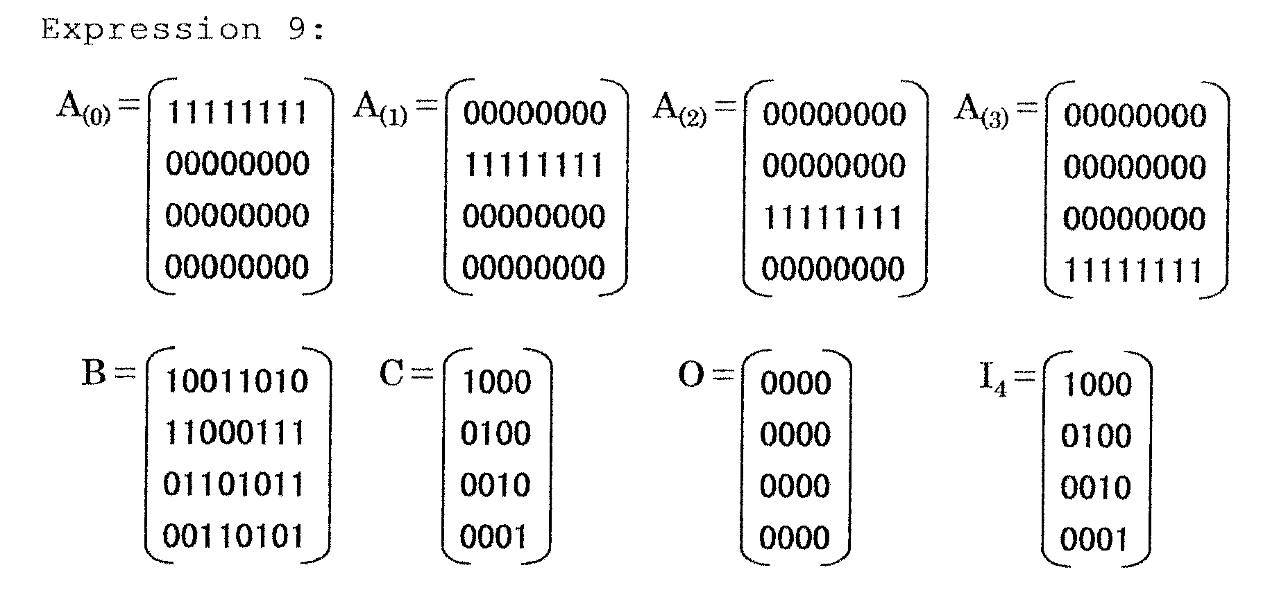

- When three column vectors are arbitrarily selected from the check matrix H of
expression 10, there is no combination such that the three column vectors are identical. Thus, the three column vectors are mutually linearly independent, and therefore in this case too, the check matrix H satisfies the aforementioned condition for it to be a check matrix for the SECDED code. How the two check matrixes (1) and (2) are selected is described later. - Hereafter, a method of conversion of the redundant portions between the byte parity code and the SECDED code is described. A vector in a field F2 in which N bits of the information portion are laterally arranged is considered. The information portion includes m bytes (each byte having n bits), as mentioned above. Thus, the vector v of the information portion may be expressed as follows:

where the component vi (j) of the information portion is either "0" or "1" (i.e., elements of the field F2={0,1}). - The vector v is further divided at byte intervals so that the byte vector vi can be defined as follows:

- Based on the above, an element vp of the byte parity code and its redundant portion p, and an element vc of the SECDED code generated based on the check matrix H and its redundant portion c are defined as vectors in a field F2 as follows:

- As needed, the redundant portion c of the SECDED code may be expressed by an m-order vector C1 and a d-order vector C2 as follows:

- By the definition of the parity, the respective components Pi of the vector p of the redundant portion of vp satisfy the following relationship with the respective components of the vector v of the information portion:

where the operator "+" indicates an addition in the field F2, i.e., an XOR operation. Similarly, the operator "+" and the term "sum" or "add" used with reference to operations among bits, matrixes, matrix elements, vectors, and vector elements refer to an XOR operation. - A necessary and sufficient condition for the vector vc as an element of the SECDED code to be a code based on the check matrix H by the definition of the code is expressed as follows:

where the "t" at upper right of the vector indicates transposition (between a row vector and a column vector). The "0" in the right-hand side of equation (3) indicates a k-order zero column vector. Equation (3) holds when there is no inverted bit (=error) in the element vc of the SECDED code. - A case where the element vc of the SECDED code contains an error is described. In this case, the result of calculation of the left-hand side of equation (3) indicates a value other than "0". Specifically, in the case of a single-bit error, the calculation result of the left-hand side of equation (3), i.e., a column vector, coincides with one of the column vectors contained in the check matrix H. A bit in the information portion v included in the element vc of the SECDED code that corresponds to the position of the coinciding column vector in the check matrix H is the error bit. Thus, the error bit can be corrected.
- In the case of a double-bit error, the column vector as a result of the calculation of the left-hand side of equation (3) is a value other than "0", as in the case of the single-bit error. However, in this case, the calculation result is a column vector of which the number of 1's included in the upper m bits is an even number (including zero). For example, as will be seen from the respective column vectors included in the check matrix H according to equations (1) and (2) of
expressions - The left-hand side member of equation (3), H.vct, may be rewritten as follows by using the elements of the check matrix H:

where the respective terms of the lower-most equation can be rewritten as follows:
- Thus, the respective terms of the lower-most equation of
expression 17 can be rewritten as follows:
- The other terms of the lower-most equation of
expression 17 can be rewritten as follows:
- Thus, the upper equation of
expression 21 can be obtained from equation (3) ofexpression 16, and equation (4) ofexpression 21 can be obtained from the upper equation ofexpression 21.
- In the above calculations, the property of the element F2 that -1=+1 is utilized.
- Equation (4) of
expression 21 is a formula for obtaining the redundant portion of the SECDED code according to the present embodiment, where the redundant portion is determined by the shape of the column vector. - It can be seen from equation (4) that the lower d bits (C2 t) of the column vector are generated from the sum of some of the components of the information portion v, and that the upper m bits (i.e., c1 t) are generated by the sum of some of the components of the lower d bits (C2 t) of the generated redundant portion and a single parity bit pt. Particularly, the lower d bits are obtained by repeated addition of the column vectors of the shape B. Vi-1 t ( i=1, ... , m) . Thus, there may be provided a single conversion circuit using the matrix B for vi-1 t, and a circuit may be realized that calculates C2 t by repeating the cycle of adding B.vi-1 t obtained by the conversion circuit while updating i. In this way, the size of the circuit for generating C2 t may be reduced to approximately 1/m of the normal size. On the other hand, when latency is given more importance, a circuit that directly obtains the polynomial B·v0 t + B.v1 t + ... + B·vm-1 t included in equation (4) may be provided. Further, the above two types of circuits may be combined into a hybrid circuit.
- Regarding the upper m bits of equation (4), the following equation is obtained:
-

- Equation (5) of
expression 22 is a formula for determining the redundant portion of the byte parity code according to the present embodiment. According to equation (5), the parity bit can be generated only from the redundant portions c1 and C2 of the SECDED code. - Focusing on one of the components of the column vectors in the right-hand side of equation (5), the number of terms required for calculating the right-hand side of equation (5) is considered. It can be seen that within the right-hand side, the maximum number of terms that appear in the first term c1 t is one, and the maximum number of terms that appear in the next term C·c2 t is d. Thus, the number of terms required for generating the parity bit according to the present embodiment is equal to or less than d+1= [log2 (n+1)]+1.
- For example, in the case of n=8, eight terms are required for generating the parity bit from
expression 15 according to the relevant technology. According to the present embodiment, d+1=[log2(8+1)]+1=[log2 9]+1=5, so that the parity bit can be generated by using a maximum of five terms. Similarly, in the case of n=16, the relevant technology requires 16 terms, whereas the present embodiment requires a maximum of [log2(16+1)]+1=6 terms. - From equation (5), it can also be seen that the number of terms that are added during the generation of the parity bit according to the present embodiment is determined by the matrix C. Therefore, in order to minimize the number of terms added, the matrix C may be selected such that "1" appears only once in the components of each column vector. Namely, in the case of a square matrix C, the matrix Cony needs to be a. permutation matrix (including a unit matrix). An example is the matrix C of expression 9 used in the check matrix H (2) of
expressions 9 and 10. The number of terms required in this case is two (see equation (2-2) ofexpression 31 as will be described later). Thus, all of the parity bits can be generated by simply calculating the sum of one each of the components c2 t and C2 t (i.e., XOR operation). This example is very effective when data stored in memory in the SECDED code format is read by converting the data into byte-parity-code format data. In this case, the circuit for such data conversion requires only one 2-input XOR circuit for each bit of the parity bits (seeFIG. 10 which will be described later). - Next, an example where n=8 and m=4 is described. In the example, the check matrix H according to equation (8) is used, and the various signs are defined as follows:

- Substituting the above into equation (4) used for generating the SECDED code yields the redundant portion c0,...,c7 of the SECDED code as shown below:

where it can be seen from equation (1-1) ofexpression 24 that, during the generation of the respective components of the column vector (c0,...,C7) of the redundant portion of the SECDED code, the maximum number of terms added is 12 (C4,...,C7) while the minimum number is 4 (C0,...,C3). Thus, 12x4 + 4x4 = 64, so that a total of 64 terms are used. - A multiple-cycle generation process is considered. It is seen from equation (1-2) of
expression 24 that each of the lower 4 bits (C4,...,C7) of the redundant portion can be generated by performing four cycles of summing of three terms. Thus, in accordance with the present embodiment, the size of the circuit for generating the SECDED code can be further reduced, and the required operations can be simplified. - For comparison purposes, a case is described in which the SECDED code of 32 bit data is generated by using a check matrix of the SECDED code according to the relevant technology. In this case, the check matrix may be selected such that the number of times of addition during code generation can be minimized. The following is an example:

- In this case, the column vector (C0,...,C6) as the redundant portion of the SECDED code is obtained as follows:

- More specifically, in the check matrix according to
expression 25, the 1st through 32nd values inrow 1 are respectively multiplied by the 32 bits of the information portion v at top ofexpression 23. As a result,row 1 of the matrix on the right-hand side ofexpression 26 is obtained as the sum of the bits of the information portion v corresponding to "1" in the 32 bits inrow 1 of the check matrix. - In the case of the example of
expression 26, in the process of generating the respective components of the redundant portion of the SECDED code, the maximum number of terms added is 15 (c6) and the minimum number is 11 (c3). Thus, the total number of terms added is 14x3 + 11 + 13x2 + 15 = 94. Because the total number of terms added in accordance with the present embodiment is 64, 94/64 = 1.46875, indicating that the relevant technology requires about 1.5 times more terms than the present embodiment. - Further, the relevant technology as illustrated by
expressions - Thus, the present embodiment requires less calculation for generating the redundant potion of the SECDED code than the relevant technology. In other words, the present embodiment is superior to the relevant technology from the viewpoint of the size of the circuit for generating the redundant portion of the SECDED code, and freedom of designing the circuit. The present embodiment is also superior to the relevant technology from the viewpoint of delay (latency) of the operating process.
- Substituting
expression 23 into equation (5) ofexpression 22 that is used in generating the redundant portion of the byte parity code yields the following:
- It can be seen from equation (1-3) that the number of terms required for generating each of the parity bits (p0,...,p3) is four in the case of the present embodiment.
- On the other hand, in the case of generating the parity bits by the relevant technology, the following equation is obtained:

- Thus, in the case of the relevant technology, the number of terms required for generating each of the parity bits (p0,...,P3) is 8, i.e., twice as many as in the case of the present embodiment illustrated by
expression 27. Thus, it can be said that the present embodiment is also superior to the relevant technology from the viewpoint of required circuit size as regards the generation of the byte parity code, for example. - In equation (4) of
expression 21 derived from the respective elements within the check matrix H according toexpression 1 for the SECDED code according to the present embodiment, the matrix B appears repeatedly. This means that a small-sized logic module can be repeatedly used in a logic process for generating the redundant portion of the SECDED code. For example, a logic verifying process may be performed on the small-sized module unit basis. In contrast, in accordance with the relevant technology using the Hamming code, the circuit for generating the redundant portion of the SECDED code does not have any specific regularity, so that the logic verifying process has to be performed on the entire check matrix. Thus, in accordance with the present embodiment, a logic verifying process for the logic circuit can be simplified compared with the relevant technology, so that verification coverage improves. - Next, a case where the check matrix (2) of
expression 10 is used is described. When equation (4) of expression 21 is calculated based on the check matrix (2), the expression (2-1) is obtained via expressions 29 and 30:

- In the logic relating to the generation of the redundant portion of the SECDED code, it is seen from equation (2-1) of
expression 30 that the maximum number of terms added (c5, c6) is 20 and the minimum number of terms added (c0,...,c3) is two. Thus, there is more variation than in the case of equation (1-2) ofexpression 24 involving the use of the check matrix (1) according toexpression 8. In the equation (2-1) as a whole, 80 terms are used, which is smaller than the number of terms required by the relevant technology (94) but more than in the case of the check matrix (1) On the other hand, substituting the check matrix (2) in equation (5) ofexpression 22 for generating the redundant portion of the byte parity code yields the following:
- It can be seen from equation (2-2) that the number of terms required for generating each of the parity bits is two. Thus, the check matrix used may be selected depending on the purpose. For example, the check matrix (1) may be used when it is desired to simplify the logic for generating the redundant portion of the SECDED code, while using the check matrix (2) when it is desired to simplify the logic for generating the redundant portion of the byte parity code.
-
FIG. 1 illustrates a circuit for generating the redundant portion of the SECDED code according to the relevant technology. The circuit is configured to realize the logic of expression 32.
where Gi (v) (i=0,....,k-1), namely Gi (i=0,..., k-1), 110, 111,...,11m-1, 11m,...,11k-1 inFIG. 1 , are functions to which the information portion v is inputted, the functions corresponding to multiple-input XOR circuits to which some of the components of the vector v are inputted. "G" in the right-hand side member of expression 32 indicates a generating matrix used for generating the redundant portion of the SECDED code. -
FIG. 2 illustrates a circuit for generating the redundant portion of the SECDED code according to the present embodiment. The circuit realizes the logic according to expressions 33 and 34.

- Expression 33 corresponds to the upper m bits of equation (4) of
expression 21. Expression 34 corresponds to the lower d bits of equation (4) ofexpression 21. - Each Ci (c2) (i=0,...,m-1) in Expression 33, i. e. , Ci(i-0,...,m-1), 130,131,...,13m-1 in
FIG. 2 , is a function to which c2 is inputted, i.e., a multiple-input XOR circuit to which some of the components of vector c2 are inputted. "C" in the right-hand side member of expression 33 indicates the matrix C defined in the definition of the check matrix H according toexpression 6. - In expression 34, each Gi (v) (i=m,...,k-1.); namely, each Gi(i=m,...,k-1), 12m,.....,12k-1 in
FIG. 2 , is a function to which the information portion v is inputted, namely a multiple-input XOR circuit to which some of the components of the vector v are inputted. - In expression 34, each Bi(vj), namely each Bi in
FIG. 2 , is a function to which vj is inputted, namely a multiple-input XOR circuit to which some of the components of the vector vj are inputted. "B" in the right-hand side member of expression 34 indicates the matrix B defined in the definition of the check matrix H ofexpression 5. -
FIG. 3 illustrates a circuit for generating the redundant portion of the byte parity code according to the relevant technology. InFIG. 3 , each pi(i=0,...,m-1) indicates each of the parity bits defined by expression 35 (same as expression 15). InFIG. 3 , each 14i(i=0,...,m-1) indicates a n-input XOR circuit to which each component vi(j) (i=0,...,m-1, j=0,...,n-1) of the information portion v is inputted.
-
FIG. 4 illustrates a circuit for generating the redundant portion of the byte parity code according to the present embodiment. The circuit realizes the logic according to expression 36.
- In
FIG. 4 , each Ci(i=0,...,m-1), 150,151,...,15m-1, i.e., each Ci (c2) (i=0,...,m-1) in expression 36, is a function to which c2 is inputted, namely a multiple-input XOR circuit to which some of the components of the vector C2 are inputted. "C" in the right-hand side member of expression 36 indicates the matrix C defined in the definition of the check matrix H according toexpression 6. - With reference to
FIGs. 5 through 10 , more specific examples of the circuit structures depicted inFIGs. 1 through 4 are described based on the assumption that the information portion is comprised of 32 bits of data where n=8 and m=4. - The 32 bits of information portion v are expressed as follows:

where the subscripts of the components of the information portion v may be expressed as follows as needed:
- The bits of the components of v according to expression 38 and the bits of the components of v according to expression 37 have the following relationship successively from the left:

- Because m=4, there are four parity bits as indicated below:

- Thus, the byte parity code (a) is expressed as follows, and the data includes 32+4=36 bits:

- Further, d=[log2(8+1)]=4 according to the following expression:

- Thus, the size of the SECDED code (ß) is a+4=36+4=40 bits. The size of the redundant portion c of the SECDED code ß is 40-32=8 bits. Further, the redundant portion c of the SECDED code ß and the SECDED code ß are expressed as follows:

- Of the redundant portion of ß, log2 (n+1) bits=ß* (i.e., d bits), are expressed as follows:

- The m bits of the redundant portion of the remaining ß is expressed as follows:

-
FIG. 5 illustrates a concrete example of the circuit structure illustrated inFIG. 1 . The example includes sevenXOR circuits 110,...,116 and is configured to realize the logic according toexpression 26. -
FIG. 6 illustrates a first example of the circuit structure illustrated inFIG. 2 . The first example is a conversion circuit (corresponding to theECC generating circuit 2 illustrated inFIGs. 11 and12 ) that generates the SECDED code from the byte parity code. The conversion circuit illustrated inFIG. 6 is based on the check matrix H expressed by equation (1) ofexpression 8, and it realizes the logic according to equations (1-1) and (1-2) ofexpression 24. InFIG. 6 , the fourXOR circuits 130,...,133 are configured to generate the upper m bits (c0,...,c3) of the redundant portion of the SECDED code, while the other fourXOR circuits 124,...,127 are configured to generate the lower d bits (c4,...,c7) of the redundant portion of the SECDED code. - In accordance with the embodiment illustrated in
FIG. 6 , the lower d bits (c4,...,c7) of the redundant portion of the SECDED code ß, i.e., log2 (n+1)=4 bits (ß*), are generated based on the information portion v of the byte parity code α. The redundant portion of the remaining ß (namely, m=4 bits) (c0,...,c3) is generated only from the parity bits (p0,....,p3) of the byte parity code α and the ß*(C4,...,c7) generated as described above. -
FIG. 7 illustrates a second example of the circuit structure illustrated inFIG. 2 . The second example is a conversion circuit (ECC generating circuit 2 inFIGs. 11 and12 ) that generates the SECDED code from the byte parity code according to the present embodiment of the present invention. The circuit ofFIG. 7 is based on the check matrix H expressed by equation (2) ofexpression 10 and configured to realize the logic according to equation (2-1) ofexpression 30. InFIG. 7 , the fourXOR circuits 13A0,...,13A3 are configured to generate the upper m bits (C0,...,C3) of the redundant portion of the SECDED code, and the other fourXOR circuits 12A4,...,12A7 are configured to generate the lower d bits (C4,...,C7) of the redundant portion of the SECDED code. - As illustrated in
FIG. 7 , in accordance with the present embodiment, as in the case ofFIG. 6 , the lower d bits (c4,...,c7) of the redundant portion of the SECDED code ß, namely log2 (n+1 ) = 4 bits (ß*), are generated based on the information portion v of the byte parity code α. The remaining redundant portion of ß (namely m= 4 bits) (c0,...,C3), are generated only from the parity bits (p0,...,p3) of the byte parity code α and the ß*(c4,...,c7) generated as described above. -
FIG. 8 illustrates a specific example of the circuit structure depicted inFIG. 3 . The example is configured to generate the byte parity code by the relevant technology. The circuit includes fourXORs 140,...,143 and is configured to realize the logic according toexpression 28. -
FIG. 9 illustrates a first example of the circuit structure illustrated inFIG. 4 . The example is a conversion circuit (corresponding to theparity generating circuit 5 inFIGs. 11 and12 ) for generating the byte parity code from the SECDED code according to the present embodiment. The circuit ofFIG. 9 is based on the check matrix H expressed by equation (1) ofexpression 8, and is configured to realize the logic of equation (1-3) ofexpression 27 by using fourXORs 150,...,153. According to the present embodiment, the circuit generates an arbitrary one of the parity bits of the byte parity code α as described above, from a number of bits equal to or less than [log2 (n+1) ]= 4 bits (as in the example ofFIG. 9 ). -
FIG. 10 illustrates a second example of the circuit structure depicted inFIG. 4 . The example is a conversion circuit (parity generating circuit 5 inFIGs. 11 and12 ) that generates the byte parity code from the SECDED code according to the present embodiment. The circuit ofFIG. 10 is based on the check matrix H expressed by equation (2) ofexpression 10, and is configured to realize the logic of equation (2-2) ofexpression 31 by using fourXORs 15A0,...,15A3. In accordance with the present embodiment, the circuit generates, as described above, an arbitrary one of the parity bits of the byte parity code α from a number of bits equal to or less than log2 (n+1)=4 bits (which is two in the example ofFIG. 10 ). -
FIG. 11 is a block diagram of a data operating unit according to an embodiment of the present invention. The data operating unit includes anoperating unit 1, anECC generating circuit 2, a memory 3, an error detecting/correctingcircuit 4, and aparity generating circuit 5. - The memory 3 stores data of the SECDED code format according to the foregoing embodiments. The
operating unit 1 reads the data from the memory 3 and executes an operating process on the data. Specifically, the error detecting/correctingcircuit 4 first performs an error detecting/correcting process on the data. The error detecting/correctingcircuit 4, which may include the RAS circuit, detects an error in the information portion of the SECDED code by using the redundant portion of the SECDED code read from the memory 3. As described above, the SECDED code is configured to enable detection and correction of a single-bit error and detection of a double-bit error. Therefore, the error detecting/correctingcircuit 4 can detect and correct a single-bit error and detect a double-bit error in the information portion of the SECDED code. After the error detecting/correcting process, the error detecting/correctingcircuit 4 delivers the SECDED code to theparity generating circuit 5. When correcting a bit error, the error detecting/correctingcircuit 4 may overwrite a corrected bit in the memory 3. - The
parity generating circuit 5 converts the SECDED code provided by the error detecting/correctingcircuit 4 into the byte parity code, and sends the byte parity code to theoperating unit 1. Theparity generating circuit 5 may have a structure illustrated inFIG. 4 . In this case, theparity generating circuit 5, based on the redundant portion of the SECDED code, generates the parity bits p0,...,pm-1 of the redundant portion of the byte parity code, using theXOR circuits 150,...,15m-1. Theparity generating circuit 5 then attaches the parity bits to the information portion of the SECDED code, thereby obtaining the byte parity code which is sent to theoperating unit 1. - The
operating unit 1 executes an operating process on the byte parity code sent from theparity generating circuit 5, and hands the processed byte parity code to theECC generating circuit 2. TheECC generating circuit 2 converts the byte parity code into the SECDED code and writes the SECDED code in the memory 3. - The
ECC generating circuit 2 may have a structure illustrated inFIG. 2 . In this case, theECC generating circuit 2, based on the information portion v of the byte parity code, generates the lower d bits (Cm,...,Ck-1) of the redundant portion of the SECDED code by using theXOR circuits 12m,...,12k-1. Then, theECC generating circuit 2, based on the lower d bits (cm,...,ck-1) of the redundant portion of the SECDED code and the parity bits (p0,...,pm-1) of the byte parity code, generates the upper m bits (c1,...,cm-1) of the redundant portion of the SECDED code by using theXOR circuits 130,...,13m-1. Then, theECC generating circuit 2 attaches the lower d bits and the upper m bits of the redundant portion of the SECDED code to the information portion of the byte parity code, thereby obtaining the SECDED code. TheECC generating circuit 2 then writes the SECDED code in the memory 3. -
FIG. 12 is a block diagram of a second example of the data operating unit. The data operating unit according to the second example is configured to give priority to the speed at which theoperating unit 1 reads data from the memory 3. - The data operating unit of the second example illustrated in
FIG. 12 includes anoperating unit 1, anECC generating circuit 2, a memory 3, an error detecting/correctingcircuit 4, and aparity generating circuit 5. TheECC generating circuit 2, the memory 3, the error detecting/correctingcircuit 4, and theparity generating circuit 5 are similar to the corresponding units or circuits of the data operating unit illustrated inFIG. 11 in structure and function. - The memory 3 stores data of the SECDED code format. The
operating unit 1 reads the data from the memory 3 and sends the data to theparity generating circuit 5. Theparity generating circuit 5 converts the SECDED code into the byte parity code by the method described with reference toFIG. 11 , and delivers the byte parity code to theoperating unit 1. The data read from the memory 3 is also simultaneously sent to the error detecting/correctingcircuit 4. The error detecting/correctingcircuit 4 performs an error detecting/correcting process on the data, i.e., the SECDED code, and notifies theoperating unit 1 about a result of the process. The error detecting/correctingcircuit 4, when correcting a bit error in the information portion of the SECDED code, may overwrite a corrected bit in the memory 3. - The
operating unit 1, based on the result of the error detecting/correcting process obtained from the error detecting/correctingcircuit 4, may perform error correction on the byte parity code sent from theparity generating circuit 5, as needed. Theoperating unit 1 performs an operating process on the byte parity code. After the operating process, theoperating unit 1 sends the byte parity code to theECC generating circuit 2. TheECC generating circuit 2 converts the byte parity code into the SECDED code by the method described with reference toFIG. 11 , and writes the SECDED code in the memory 3. - All examples and conditional language recited herein are intended for pedagogical purposes to aid the reader in understanding the invention and the concepts contributed by the inventor to furthering the art, and are to be construed as being without limitation to such specifically recited examples and conditions, nor does the organization of such examples in the specification relate to a showing of the superiority or inferiority of the invention. Although the embodiments of the present inventions have been described in detail, it should be understood that the various changes, substitutions, and alterations could be made hereto without departing from the spirit and scope of the invention.
Claims (9)
- An error detecting/correcting code generating circuit comprising:a first Exclusive-OR operation circuit that generates log2(n+1) bits of one portion of a redundant portion of error detecting/correcting-code-attached data by rounding the numbers to the right of the decimal point of log2(n+1) in response to the input of m bytes of an information portion included in error-detection-bit-attached data,the error-detection-bit-attached data including a redundant portion of m bits of error detection bits allocated to the m bytes of the information portion, the byte having n bits; anda second Exclusive-OR operation circuit that generates m bits of another portion of the redundant portion of the error detecting/correcting-code-attached data in response to the input of the one portion and the error detection bits.
- The error detecting/correcting code generating circuit according to claim 1, wherein,
when each of the bytes of the information portion of the error-detection-bit-attached data is expressed by a byte vector having n elements, and the information portion of the error-detection-bit-attached data is expressed by an information vector having m elements,
the first Exclusive-OR operation unit generates the one portion in response to the input of a value of the information vector, and
the second Exclusive-OR operation unit generates the other portion in response to the input of the one portion and the error detecting bits,in accordance with an error detecting/correcting code generating formula for generating a vector of the one portion and a vector of the other portion by a matrix operation of the information vector and the error detection bits. - The error detecting/correcting code generating circuit according to claim 1, wherein
the error detecting/correcting-code-attached data has (n+1) m + [log2 (n+1) ] bits of which the mn bits constitute the information portion and of which the other m + [log2 (n+1) ] bits constitute the redundant portion, where [log2(n+1)] indicates log2(n+1) from which the numbers to the right of the decimal point have been rounded,the circuit further comprising:a third Exclusive-OR operating circuit that generates the error detection bits in response to the input of a maximum of [log2(n+1)] bits of the redundant portion. - The error detecting/correcting code generating circuit according to claim 2, wherein,
when each of the bytes of the information portion of the error-detection-bit-attached data is expressed by a byte vector vi(Vi(0),vi(1),...,vi(n-2), Vi(n-1)) having n elements, the information portion of the error-detection-bit-attached data is expressed by an information vector v(v0,v1,...,vm-1) having m elements, the redundant portion of the error-detection-bit-attached data is expressed by m bits of error detection bits p (p0, p1,..., pm-2, pm-1) allocated to element of the information vector having the m elements, and the error-detection-bit-attached is expressed by a byte parity code vp(v,p),
the first Exclusive-OR operation unit gen a value of a d-order vector C2 which is the one portion of the redundant portion of the error detecting/correcting-code-attached data, and
the second Exclusive-OR operation unit generates a value of an m-order vector c1 which is the other portion of the redundant portion of the error detecting/correcting-code-attached data,
in response to the input of a value of the information vector v (v0, v1,..., vm-1) and a value error detection bits p (p0,p1,...,pm-2,pm-1) of the parity code vp(v,p), and
in accordance with the error detecting/correcting code generating formula which expressed by the following:
wherein each bit pi of the error detection bits p(p0,p1,...,pm-2,pm-1) and the byte vector vi (vi(0), vi(1),...,vi(n-2), vi(n-1)) of each element of the information vector v(v0,v1,...,vm-1) have the following relationship:
where "+" indicates an Exclusive-OR operation and "t" indicates a transposition of a matrix. - An error detection bit generating circuit in which error detecting/correcting-code-attached data has (n+1) m + [ log2 (n+1) ] bits including mn bits of an information portion and a redundant portion, the redundant portion including one portion of [log2(n+1)] bits and another portion of m bits, log2(n+1)] indicating log2(n+1) from which the numbers to the right of the decimal point have been rounded, the circuit comprising:an Exclusive-OR operation circuit that generates an error detection bit in response to the input of the data having a maximum of [log2(n+1)] bits of the redundant portion.
- A method of controlling an error detecting/correcting code generating circuit, the method comprising:generating one portion of log2(n+1) bits of a redundant portion of error detecting/correcting-code-attached data by rounding the numbers to the right of the decimal point of log2(n+1) in response to the input of m bytes of an information portion included in error-detection-bit-attached data, using a first Exclusive-OR operation circuit of the error detecting/correcting code generating circuit, the error-detection-bit-attached data further including a redundant portion of m bits of error detection bits allocated to the m bytes of the information portion, each of the bytes having n bits; andgenerating another portion of m bits of the redundant portion of the error detecting-code-attached data in response to the input of the log2(n+1) bits of the one portion and the error detection bits, using a second Exclusive-OR operation circuit of the error detecting/correcting code generating circuit.
- The method of controlling the error detecting/correcting code generating circuit according to claim 6, wherein
when each of the bytes of the information portion of the error-detection-bit-attached data is expressed by a byte vector having n elements, and the information portion of the error-detection-bit-attached data is expressed by an information vector having m elements,
the generating of the one portion of log2 (n+1) bits includes generating the one portion in response to the input of the information vector in accordance with an error detecting/correcting code generating formula, and
the generating of the m bits of the other portion includes generating the other portion in response to the input of the one portion and the error detection bits in accordance with the error detecting/correcting code generating formula,
wherein the error detecting/correcting code generating formula generates a vector of the one portion and a vector of the other portion by a matrix operation of the information vector and the error detection bits. - The method of controlling the error detecting/correcting code generating circuit according to claim 6, wherein
the error detecting/correcting-code-attached data has (n+1)m+[log2(n+1)] bits of which the mn bits constitute the information portion and of which the other m + [ log2 (n+1) ] bits constitute the redundant portion,
[log2(n+1)] indicating log2(n+1) from which the numbers to the right of the decimal point have been rounded,
the method further comprising:generating each of the error detection bits in response to the input of a maximum of [log2(n+1)] bits of the redundant portion, using a third Exclusive-OR operation circuit of the error detecting/correcting code generating circuit. - The method of controlling the error detecting/correcting code generating circuit according to claim 7, wherein
when each of the bytes of the information portion of the error-detection-bit-attached data is expressed by a byte vector vi(vi(0),vi(1),..., vi(n-2), vi(n-1)) having n elements,
the information portion of the error-detection-bit-attached data is expressed by an information vector v (v0, v1,..., vm-1) having m elements,
the redundant portion of the error-detection-bit-attached data is expressed by m bits of an error detection bit p(p0, p1,..., pm-2, pm-1) allocated to each element of the information vector having the m elements, and the error-detection-bit-attached data is expressed by a byte parity code vp(v,p),
the generating of the one portion of log2(n+1) bits includes generating a d-order vector c2 of the one portion of the redundant portion of the error detecting/correcting-code-attached data, and
the generating of the m bits of the other portion includes generating an m-order vector c1 of the other portion of the redundant portion of the error detecting/correcting-code-attached data,
in response to the input of the information vector v (v0, v1,..., vm-1) and the error detection bit p(p0,p1,...,pm-2, pm-1) of the byte parity code vp (v,p), and
in accordance with the error
detecting/correcting code generating formula expressed by the following:
wherein each bit pi of the error detection bit p(p0, p1,..., pm-2, pm-1) and the byte vector vi (vi(0), vi(1),..., vi(n-2), vi(n-1)) of each element of the information vector v(v0,v1,...,vm-1) have the following relationship:
where "+" indicates an Exclusive-OR operation and "t" indicates a transposition of a matrix.
Applications Claiming Priority (1)
| Application Number | Priority Date | Filing Date | Title |
|---|---|---|---|
| JP2009263229A JP5353655B2 (en) | 2009-11-18 | 2009-11-18 | Error detection / correction code generation circuit and control method thereof |
Publications (3)
| Publication Number | Publication Date |
|---|---|
| EP2326014A2 true EP2326014A2 (en) | 2011-05-25 |
| EP2326014A3 EP2326014A3 (en) | 2013-01-02 |
| EP2326014B1 EP2326014B1 (en) | 2020-01-01 |
Family
ID=43734301
Family Applications (1)
| Application Number | Title | Priority Date | Filing Date |
|---|---|---|---|
| EP10189814.6A Active EP2326014B1 (en) | 2009-11-18 | 2010-11-03 | Error detecting/correcting code generating circuit and method of controlling the same |
Country Status (3)
| Country | Link |
|---|---|
| US (1) | US8539302B2 (en) |
| EP (1) | EP2326014B1 (en) |
| JP (1) | JP5353655B2 (en) |
Cited By (1)
| Publication number | Priority date | Publication date | Assignee | Title |
|---|---|---|---|---|
| EP3799449A1 (en) * | 2019-09-30 | 2021-03-31 | Beijing Baidu Netcom Science And Technology Co., Ltd. | Method, apparatus, device, and medium for verifying vehicle information |
Families Citing this family (5)
| Publication number | Priority date | Publication date | Assignee | Title |
|---|---|---|---|---|
| US9450613B2 (en) | 2010-11-10 | 2016-09-20 | Infineon Technologies Ag | Apparatus and method for error correction and error detection |
| US8539321B2 (en) * | 2010-11-10 | 2013-09-17 | Infineon Technologies Ag | Apparatus and method for correcting at least one bit error within a coded bit sequence |
| JP2013070122A (en) | 2011-09-20 | 2013-04-18 | Fujitsu Ltd | Error correction device, error correction method and arithmetic unit |
| JP5674700B2 (en) | 2012-03-22 | 2015-02-25 | 株式会社東芝 | Encoding apparatus, control method of encoding apparatus, and storage device |
| US10725841B1 (en) * | 2017-12-18 | 2020-07-28 | Xilinx, Inc. | Method and apparatus for error detection and correction |
Citations (2)
| Publication number | Priority date | Publication date | Assignee | Title |
|---|---|---|---|---|
| JPS4866334A (en) | 1971-12-13 | 1973-09-11 | ||
| US5313475A (en) | 1991-10-31 | 1994-05-17 | International Business Machines Corporation | ECC function with self-contained high performance partial write or read/modify/write and parity look-ahead interface scheme |
Family Cites Families (13)
| Publication number | Priority date | Publication date | Assignee | Title |
|---|---|---|---|---|
| US3648239A (en) * | 1970-06-30 | 1972-03-07 | Ibm | System for translating to and from single error correction-double error detection hamming code and byte parity code |
| JPS554775A (en) * | 1978-06-27 | 1980-01-14 | Nec Corp | Generation and check circuit for hamming code for storage device |
| US4241446A (en) * | 1978-10-16 | 1980-12-23 | Honeywell Information Systems Inc. | Apparatus for performing single error correction and double error detection |
| US4345328A (en) * | 1980-06-30 | 1982-08-17 | Sperry Corporation | ECC Check bit generation using through checking parity bits |
| US5291498A (en) * | 1991-01-29 | 1994-03-01 | Convex Computer Corporation | Error detecting method and apparatus for computer memory having multi-bit output memory circuits |
| US5617432A (en) * | 1994-11-09 | 1997-04-01 | International Business Machines Corporation | Common error protection code for data stored as a composite of different data formats |
| US5942002A (en) * | 1996-03-08 | 1999-08-24 | Neo-Lore | Method and apparatus for generating a transform |
| US6675349B1 (en) * | 2000-05-11 | 2004-01-06 | International Business Machines Corporation | Error correction coding of data blocks with included parity bits |
| US6981195B2 (en) * | 2002-08-02 | 2005-12-27 | Analog Devices, Inc. | Cyclic redundancy check with efficient re-computation of error detection code |
| US7143332B1 (en) * | 2003-12-16 | 2006-11-28 | Xilinx, Inc. | Methods and structures for providing programmable width and error correction in memory arrays in programmable logic devices |
| US8261167B1 (en) * | 2009-03-09 | 2012-09-04 | Pmc-Sierra Us, Inc. | Cyclically interleaved dual BCH, with simultaneous decode and per-codeword maximum likelihood reconciliation |
| US8301972B2 (en) * | 2009-05-27 | 2012-10-30 | Seagate Technology Llc | Apparatus for correcting single bit insertion or deletion in a data payload with a checksum corrector |
| US8381083B2 (en) * | 2009-10-22 | 2013-02-19 | Arm Limited | Error control coding for single error correction and double error detection |
-
2009
- 2009-11-18 JP JP2009263229A patent/JP5353655B2/en active Active
-
2010
- 2010-11-03 EP EP10189814.6A patent/EP2326014B1/en active Active
- 2010-11-18 US US12/948,816 patent/US8539302B2/en active Active
Patent Citations (3)
| Publication number | Priority date | Publication date | Assignee | Title |
|---|---|---|---|---|
| JPS4866334A (en) | 1971-12-13 | 1973-09-11 | ||
| US5313475A (en) | 1991-10-31 | 1994-05-17 | International Business Machines Corporation | ECC function with self-contained high performance partial write or read/modify/write and parity look-ahead interface scheme |
| JPH06324951A (en) | 1991-10-31 | 1994-11-25 | Internatl Business Mach Corp <Ibm> | Computer system with error inspection / correction function |
Cited By (2)
| Publication number | Priority date | Publication date | Assignee | Title |
|---|---|---|---|---|
| EP3799449A1 (en) * | 2019-09-30 | 2021-03-31 | Beijing Baidu Netcom Science And Technology Co., Ltd. | Method, apparatus, device, and medium for verifying vehicle information |
| US11375376B2 (en) | 2019-09-30 | 2022-06-28 | Apollo Intelligent Driving Technology (Beijing) Co., Ltd. | Method, apparatus, device, and medium for verifying vehicle information |
Also Published As
| Publication number | Publication date |
|---|---|
| US8539302B2 (en) | 2013-09-17 |
| EP2326014A3 (en) | 2013-01-02 |
| JP5353655B2 (en) | 2013-11-27 |
| JP2011109476A (en) | 2011-06-02 |
| EP2326014B1 (en) | 2020-01-01 |
| US20110119559A1 (en) | 2011-05-19 |
Similar Documents
| Publication | Publication Date | Title |
|---|---|---|
| Krishna et al. | Computational Number Theory and Digital Signal Processing: Fast Algorithms and Error Control Techniques | |
| JP4036338B2 (en) | Method and apparatus for correcting and detecting multiple spotty byte errors in a byte with a limited number of error bytes | |
| US8489916B2 (en) | Multi-disk fault-tolerant system, method for generating a check block, and method for recovering a data block | |
| US8775899B2 (en) | Error correction device, error correction method, and processor | |
| EP2326014B1 (en) | Error detecting/correcting code generating circuit and method of controlling the same | |
| KR100953884B1 (en) | How to handle multiplication of RAID device and galloche | |
| JP4288486B2 (en) | Disk array device, RAID parity data generation circuit, and Galois field multiplication circuit | |
| US20210218419A1 (en) | Method, device and apparatus for storing data, computer readable storage medium | |
| US7350126B2 (en) | Method for constructing erasure correcting codes whose implementation requires only exclusive ORs | |
| JPH02278921A (en) | Method for encoding and decoding binary data and decoder | |
| Huang et al. | On optimizing XOR-based codes for fault-tolerant storage applications | |
| US8739006B2 (en) | Reduced circuit implementation of encoder and syndrome generator | |
| US7797612B2 (en) | Storage accelerator | |
| US20020188909A1 (en) | Symbol level error correction codes which protect against memory chip and bus line failures | |
| Reyhani-Masoleh et al. | Towards fault-tolerant cryptographic computations over finite fields | |
| US4868829A (en) | Apparatus useful for correction of single bit errors in the transmission of data | |
| US8499224B2 (en) | Redundant code generation method and device, data restoration method and device, and raid storage device | |
| US20260104859A1 (en) | Processing unit, processing-in-memory device, and processing-in-memory system based on redundant residue number system | |
| Parhami | Parity-preserving transformations in computer arithmetic | |
| US10623018B2 (en) | Method of arrangement of an algorithm in cyclic redundancy check | |
| Zanitti et al. | Decoding Algorithms for Symbol-Error Correction in MDS Array Codes via Superregular Matrices | |
| JP2006101429A (en) | Intrabyte multiple spotty byte error correction / detection method and apparatus | |
| Bortolussi et al. | Possibilistic coding: error detection vs. error correction | |
| KR20260052754A (en) | Processing Unit, Processing-In-Memory Device, and Processing-In-Memory System Based on Redundant Residue Number System | |
| Tsai et al. | TAIWAN Online: Test AI with AN Codes Online for Automotive Chips |
Legal Events
| Date | Code | Title | Description |
|---|---|---|---|
| PUAI | Public reference made under article 153(3) epc to a published international application that has entered the european phase |
Free format text: ORIGINAL CODE: 0009012 |
|
| AK | Designated contracting states |
Kind code of ref document: A2 Designated state(s): AL AT BE BG CH CY CZ DE DK EE ES FI FR GB GR HR HU IE IS IT LI LT LU LV MC MK MT NL NO PL PT RO RS SE SI SK SM TR |
|
| AX | Request for extension of the european patent |
Extension state: BA ME |
|
| PUAL | Search report despatched |
Free format text: ORIGINAL CODE: 0009013 |
|
| AK | Designated contracting states |
Kind code of ref document: A3 Designated state(s): AL AT BE BG CH CY CZ DE DK EE ES FI FR GB GR HR HU IE IS IT LI LT LU LV MC MK MT NL NO PL PT RO RS SE SI SK SM TR |
|
| AX | Request for extension of the european patent |
Extension state: BA ME |
|
| RIC1 | Information provided on ipc code assigned before grant |
Ipc: H03M 13/19 20060101ALI20121128BHEP Ipc: H03M 13/05 20060101ALI20121128BHEP Ipc: H03M 13/09 20060101AFI20121128BHEP Ipc: G06F 11/00 20060101ALI20121128BHEP Ipc: G06F 11/10 20060101ALI20121128BHEP |
|
| 17P | Request for examination filed |
Effective date: 20130327 |
|
| 17Q | First examination report despatched |
Effective date: 20160330 |
|
| STAA | Information on the status of an ep patent application or granted ep patent |
Free format text: STATUS: EXAMINATION IS IN PROGRESS |
|
| REG | Reference to a national code |
Ref country code: DE Ref legal event code: R079 Ref document number: 602010062596 Country of ref document: DE Free format text: PREVIOUS MAIN CLASS: H03M0013090000 Ipc: H03M0013190000 |
|
| GRAP | Despatch of communication of intention to grant a patent |
Free format text: ORIGINAL CODE: EPIDOSNIGR1 |
|
| STAA | Information on the status of an ep patent application or granted ep patent |
Free format text: STATUS: GRANT OF PATENT IS INTENDED |
|
| RIC1 | Information provided on ipc code assigned before grant |
Ipc: H03M 13/00 20060101ALI20190708BHEP Ipc: H03M 13/19 20060101AFI20190708BHEP Ipc: H03M 13/03 20060101ALI20190708BHEP |
|
| INTG | Intention to grant announced |
Effective date: 20190729 |
|
| GRAS | Grant fee paid |
Free format text: ORIGINAL CODE: EPIDOSNIGR3 |
|
| GRAA | (expected) grant |
Free format text: ORIGINAL CODE: 0009210 |
|
| STAA | Information on the status of an ep patent application or granted ep patent |
Free format text: STATUS: THE PATENT HAS BEEN GRANTED |
|
| AK | Designated contracting states |
Kind code of ref document: B1 Designated state(s): AL AT BE BG CH CY CZ DE DK EE ES FI FR GB GR HR HU IE IS IT LI LT LU LV MC MK MT NL NO PL PT RO RS SE SI SK SM TR |
|
| REG | Reference to a national code |
Ref country code: GB Ref legal event code: FG4D |
|
| REG | Reference to a national code |
Ref country code: AT Ref legal event code: REF Ref document number: 1221080 Country of ref document: AT Kind code of ref document: T Effective date: 20200115 Ref country code: CH Ref legal event code: EP |
|
| REG | Reference to a national code |
Ref country code: IE Ref legal event code: FG4D |
|
| REG | Reference to a national code |
Ref country code: DE Ref legal event code: R096 Ref document number: 602010062596 Country of ref document: DE |
|
| REG | Reference to a national code |
Ref country code: NL Ref legal event code: MP Effective date: 20200101 |
|
| REG | Reference to a national code |
Ref country code: LT Ref legal event code: MG4D |
|
| PG25 | Lapsed in a contracting state [announced via postgrant information from national office to epo] |
Ref country code: RS Free format text: LAPSE BECAUSE OF FAILURE TO SUBMIT A TRANSLATION OF THE DESCRIPTION OR TO PAY THE FEE WITHIN THE PRESCRIBED TIME-LIMIT Effective date: 20200101 Ref country code: FI Free format text: LAPSE BECAUSE OF FAILURE TO SUBMIT A TRANSLATION OF THE DESCRIPTION OR TO PAY THE FEE WITHIN THE PRESCRIBED TIME-LIMIT Effective date: 20200101 Ref country code: NL Free format text: LAPSE BECAUSE OF FAILURE TO SUBMIT A TRANSLATION OF THE DESCRIPTION OR TO PAY THE FEE WITHIN THE PRESCRIBED TIME-LIMIT Effective date: 20200101 Ref country code: LT Free format text: LAPSE BECAUSE OF FAILURE TO SUBMIT A TRANSLATION OF THE DESCRIPTION OR TO PAY THE FEE WITHIN THE PRESCRIBED TIME-LIMIT Effective date: 20200101 Ref country code: CZ Free format text: LAPSE BECAUSE OF FAILURE TO SUBMIT A TRANSLATION OF THE DESCRIPTION OR TO PAY THE FEE WITHIN THE PRESCRIBED TIME-LIMIT Effective date: 20200101 Ref country code: NO Free format text: LAPSE BECAUSE OF FAILURE TO SUBMIT A TRANSLATION OF THE DESCRIPTION OR TO PAY THE FEE WITHIN THE PRESCRIBED TIME-LIMIT Effective date: 20200401 Ref country code: PT Free format text: LAPSE BECAUSE OF FAILURE TO SUBMIT A TRANSLATION OF THE DESCRIPTION OR TO PAY THE FEE WITHIN THE PRESCRIBED TIME-LIMIT Effective date: 20200527 |
|
| PG25 | Lapsed in a contracting state [announced via postgrant information from national office to epo] |
Ref country code: IS Free format text: LAPSE BECAUSE OF FAILURE TO SUBMIT A TRANSLATION OF THE DESCRIPTION OR TO PAY THE FEE WITHIN THE PRESCRIBED TIME-LIMIT Effective date: 20200501 Ref country code: SE Free format text: LAPSE BECAUSE OF FAILURE TO SUBMIT A TRANSLATION OF THE DESCRIPTION OR TO PAY THE FEE WITHIN THE PRESCRIBED TIME-LIMIT Effective date: 20200101 Ref country code: LV Free format text: LAPSE BECAUSE OF FAILURE TO SUBMIT A TRANSLATION OF THE DESCRIPTION OR TO PAY THE FEE WITHIN THE PRESCRIBED TIME-LIMIT Effective date: 20200101 Ref country code: HR Free format text: LAPSE BECAUSE OF FAILURE TO SUBMIT A TRANSLATION OF THE DESCRIPTION OR TO PAY THE FEE WITHIN THE PRESCRIBED TIME-LIMIT Effective date: 20200101 Ref country code: GR Free format text: LAPSE BECAUSE OF FAILURE TO SUBMIT A TRANSLATION OF THE DESCRIPTION OR TO PAY THE FEE WITHIN THE PRESCRIBED TIME-LIMIT Effective date: 20200402 Ref country code: BG Free format text: LAPSE BECAUSE OF FAILURE TO SUBMIT A TRANSLATION OF THE DESCRIPTION OR TO PAY THE FEE WITHIN THE PRESCRIBED TIME-LIMIT Effective date: 20200401 |
|
| REG | Reference to a national code |
Ref country code: DE Ref legal event code: R097 Ref document number: 602010062596 Country of ref document: DE |
|
| PG25 | Lapsed in a contracting state [announced via postgrant information from national office to epo] |
Ref country code: SK Free format text: LAPSE BECAUSE OF FAILURE TO SUBMIT A TRANSLATION OF THE DESCRIPTION OR TO PAY THE FEE WITHIN THE PRESCRIBED TIME-LIMIT Effective date: 20200101 Ref country code: SM Free format text: LAPSE BECAUSE OF FAILURE TO SUBMIT A TRANSLATION OF THE DESCRIPTION OR TO PAY THE FEE WITHIN THE PRESCRIBED TIME-LIMIT Effective date: 20200101 Ref country code: EE Free format text: LAPSE BECAUSE OF FAILURE TO SUBMIT A TRANSLATION OF THE DESCRIPTION OR TO PAY THE FEE WITHIN THE PRESCRIBED TIME-LIMIT Effective date: 20200101 Ref country code: RO Free format text: LAPSE BECAUSE OF FAILURE TO SUBMIT A TRANSLATION OF THE DESCRIPTION OR TO PAY THE FEE WITHIN THE PRESCRIBED TIME-LIMIT Effective date: 20200101 Ref country code: DK Free format text: LAPSE BECAUSE OF FAILURE TO SUBMIT A TRANSLATION OF THE DESCRIPTION OR TO PAY THE FEE WITHIN THE PRESCRIBED TIME-LIMIT Effective date: 20200101 Ref country code: ES Free format text: LAPSE BECAUSE OF FAILURE TO SUBMIT A TRANSLATION OF THE DESCRIPTION OR TO PAY THE FEE WITHIN THE PRESCRIBED TIME-LIMIT Effective date: 20200101 |
|
| PLBE | No opposition filed within time limit |
Free format text: ORIGINAL CODE: 0009261 |
|
| STAA | Information on the status of an ep patent application or granted ep patent |
Free format text: STATUS: NO OPPOSITION FILED WITHIN TIME LIMIT |
|
| REG | Reference to a national code |
Ref country code: AT Ref legal event code: MK05 Ref document number: 1221080 Country of ref document: AT Kind code of ref document: T Effective date: 20200101 |
|
| 26N | No opposition filed |
Effective date: 20201002 |
|
| REG | Reference to a national code |
Ref country code: DE Ref legal event code: R082 Ref document number: 602010062596 Country of ref document: DE Representative=s name: HL KEMPNER PATENTANWAELTE, SOLICITORS (ENGLAND, DE Ref country code: DE Ref legal event code: R082 Ref document number: 602010062596 Country of ref document: DE Representative=s name: HL KEMPNER PARTG MBB, DE Ref country code: DE Ref legal event code: R082 Ref document number: 602010062596 Country of ref document: DE Representative=s name: HL KEMPNER PATENTANWALT, RECHTSANWALT, SOLICIT, DE |
|
| PG25 | Lapsed in a contracting state [announced via postgrant information from national office to epo] |
Ref country code: AT Free format text: LAPSE BECAUSE OF FAILURE TO SUBMIT A TRANSLATION OF THE DESCRIPTION OR TO PAY THE FEE WITHIN THE PRESCRIBED TIME-LIMIT Effective date: 20200101 Ref country code: IT Free format text: LAPSE BECAUSE OF FAILURE TO SUBMIT A TRANSLATION OF THE DESCRIPTION OR TO PAY THE FEE WITHIN THE PRESCRIBED TIME-LIMIT Effective date: 20200101 |
|
| PG25 | Lapsed in a contracting state [announced via postgrant information from national office to epo] |
Ref country code: SI Free format text: LAPSE BECAUSE OF FAILURE TO SUBMIT A TRANSLATION OF THE DESCRIPTION OR TO PAY THE FEE WITHIN THE PRESCRIBED TIME-LIMIT Effective date: 20200101 Ref country code: PL Free format text: LAPSE BECAUSE OF FAILURE TO SUBMIT A TRANSLATION OF THE DESCRIPTION OR TO PAY THE FEE WITHIN THE PRESCRIBED TIME-LIMIT Effective date: 20200101 |
|
| PG25 | Lapsed in a contracting state [announced via postgrant information from national office to epo] |
Ref country code: MC Free format text: LAPSE BECAUSE OF FAILURE TO SUBMIT A TRANSLATION OF THE DESCRIPTION OR TO PAY THE FEE WITHIN THE PRESCRIBED TIME-LIMIT Effective date: 20200101 |
|
| REG | Reference to a national code |
Ref country code: CH Ref legal event code: PL |
|
| PG25 | Lapsed in a contracting state [announced via postgrant information from national office to epo] |
Ref country code: LU Free format text: LAPSE BECAUSE OF NON-PAYMENT OF DUE FEES Effective date: 20201103 |
|
| REG | Reference to a national code |
Ref country code: BE Ref legal event code: MM Effective date: 20201130 |
|
| PG25 | Lapsed in a contracting state [announced via postgrant information from national office to epo] |
Ref country code: LI Free format text: LAPSE BECAUSE OF NON-PAYMENT OF DUE FEES Effective date: 20201130 Ref country code: CH Free format text: LAPSE BECAUSE OF NON-PAYMENT OF DUE FEES Effective date: 20201130 |
|
| PG25 | Lapsed in a contracting state [announced via postgrant information from national office to epo] |
Ref country code: IE Free format text: LAPSE BECAUSE OF NON-PAYMENT OF DUE FEES Effective date: 20201103 |
|
| PG25 | Lapsed in a contracting state [announced via postgrant information from national office to epo] |
Ref country code: TR Free format text: LAPSE BECAUSE OF FAILURE TO SUBMIT A TRANSLATION OF THE DESCRIPTION OR TO PAY THE FEE WITHIN THE PRESCRIBED TIME-LIMIT Effective date: 20200101 Ref country code: MT Free format text: LAPSE BECAUSE OF FAILURE TO SUBMIT A TRANSLATION OF THE DESCRIPTION OR TO PAY THE FEE WITHIN THE PRESCRIBED TIME-LIMIT Effective date: 20200101 Ref country code: CY Free format text: LAPSE BECAUSE OF FAILURE TO SUBMIT A TRANSLATION OF THE DESCRIPTION OR TO PAY THE FEE WITHIN THE PRESCRIBED TIME-LIMIT Effective date: 20200101 |
|
| PG25 | Lapsed in a contracting state [announced via postgrant information from national office to epo] |
Ref country code: MK Free format text: LAPSE BECAUSE OF FAILURE TO SUBMIT A TRANSLATION OF THE DESCRIPTION OR TO PAY THE FEE WITHIN THE PRESCRIBED TIME-LIMIT Effective date: 20200101 Ref country code: AL Free format text: LAPSE BECAUSE OF FAILURE TO SUBMIT A TRANSLATION OF THE DESCRIPTION OR TO PAY THE FEE WITHIN THE PRESCRIBED TIME-LIMIT Effective date: 20200101 |
|
| PG25 | Lapsed in a contracting state [announced via postgrant information from national office to epo] |
Ref country code: BE Free format text: LAPSE BECAUSE OF NON-PAYMENT OF DUE FEES Effective date: 20201130 |
|
| PGFP | Annual fee paid to national office [announced via postgrant information from national office to epo] |
Ref country code: DE Payment date: 20251022 Year of fee payment: 16 |
|
| PGFP | Annual fee paid to national office [announced via postgrant information from national office to epo] |
Ref country code: GB Payment date: 20251023 Year of fee payment: 16 |
|
| PGFP | Annual fee paid to national office [announced via postgrant information from national office to epo] |
Ref country code: FR Payment date: 20251022 Year of fee payment: 16 |