EP2325994A2 - Power conversion equipment - Google Patents
Power conversion equipment Download PDFInfo
- Publication number
- EP2325994A2 EP2325994A2 EP10189050A EP10189050A EP2325994A2 EP 2325994 A2 EP2325994 A2 EP 2325994A2 EP 10189050 A EP10189050 A EP 10189050A EP 10189050 A EP10189050 A EP 10189050A EP 2325994 A2 EP2325994 A2 EP 2325994A2
- Authority
- EP
- European Patent Office
- Prior art keywords
- alternating current
- voltage
- capacitor
- capacitors
- series circuit
- Prior art date
- Legal status (The legal status is an assumption and is not a legal conclusion. Google has not performed a legal analysis and makes no representation as to the accuracy of the status listed.)
- Withdrawn
Links
Images




Classifications
-
- H—ELECTRICITY
- H02—GENERATION; CONVERSION OR DISTRIBUTION OF ELECTRIC POWER
- H02M—APPARATUS FOR CONVERSION BETWEEN AC AND AC, BETWEEN AC AND DC, OR BETWEEN DC AND DC, AND FOR USE WITH MAINS OR SIMILAR POWER SUPPLY SYSTEMS; CONVERSION OF DC OR AC INPUT POWER INTO SURGE OUTPUT POWER; CONTROL OR REGULATION THEREOF
- H02M7/00—Conversion of AC power input into DC power output; Conversion of DC power input into AC power output
- H02M7/42—Conversion of DC power input into AC power output without possibility of reversal
- H02M7/44—Conversion of DC power input into AC power output without possibility of reversal by static converters
- H02M7/48—Conversion of DC power input into AC power output without possibility of reversal by static converters using discharge tubes with control electrode or semiconductor devices with control electrode
- H02M7/483—Converters with outputs that each can have more than two voltages levels
- H02M7/487—Neutral point clamped inverters
-
- H—ELECTRICITY
- H02—GENERATION; CONVERSION OR DISTRIBUTION OF ELECTRIC POWER
- H02M—APPARATUS FOR CONVERSION BETWEEN AC AND AC, BETWEEN AC AND DC, OR BETWEEN DC AND DC, AND FOR USE WITH MAINS OR SIMILAR POWER SUPPLY SYSTEMS; CONVERSION OF DC OR AC INPUT POWER INTO SURGE OUTPUT POWER; CONTROL OR REGULATION THEREOF
- H02M7/00—Conversion of AC power input into DC power output; Conversion of DC power input into AC power output
- H02M7/42—Conversion of DC power input into AC power output without possibility of reversal
- H02M7/44—Conversion of DC power input into AC power output without possibility of reversal by static converters
- H02M7/48—Conversion of DC power input into AC power output without possibility of reversal by static converters using discharge tubes with control electrode or semiconductor devices with control electrode
- H02M7/53—Conversion of DC power input into AC power output without possibility of reversal by static converters using discharge tubes with control electrode or semiconductor devices with control electrode using devices of a triode or transistor type requiring continuous application of a control signal
- H02M7/537—Conversion of DC power input into AC power output without possibility of reversal by static converters using discharge tubes with control electrode or semiconductor devices with control electrode using devices of a triode or transistor type requiring continuous application of a control signal using semiconductor devices only, e.g. single switched pulse inverters
- H02M7/5387—Conversion of DC power input into AC power output without possibility of reversal by static converters using discharge tubes with control electrode or semiconductor devices with control electrode using devices of a triode or transistor type requiring continuous application of a control signal using semiconductor devices only, e.g. single switched pulse inverters in a bridge configuration
- H02M7/53871—Conversion of DC power input into AC power output without possibility of reversal by static converters using discharge tubes with control electrode or semiconductor devices with control electrode using devices of a triode or transistor type requiring continuous application of a control signal using semiconductor devices only, e.g. single switched pulse inverters in a bridge configuration with automatic control of output voltage or current
- H02M7/53875—Conversion of DC power input into AC power output without possibility of reversal by static converters using discharge tubes with control electrode or semiconductor devices with control electrode using devices of a triode or transistor type requiring continuous application of a control signal using semiconductor devices only, e.g. single switched pulse inverters in a bridge configuration with automatic control of output voltage or current with analogue control of three-phase output
- H02M7/53876—Conversion of DC power input into AC power output without possibility of reversal by static converters using discharge tubes with control electrode or semiconductor devices with control electrode using devices of a triode or transistor type requiring continuous application of a control signal using semiconductor devices only, e.g. single switched pulse inverters in a bridge configuration with automatic control of output voltage or current with analogue control of three-phase output based on synthesising a desired voltage vector via the selection of appropriate fundamental voltage vectors, and corresponding dwelling times
Definitions
- the present invention relates to a multilevel inverter that outputs an alternating current voltage having three or more different potentials in a half-cycle period, and in particular, relates to a technology for balancing the voltage of each capacitor in a capacitor series circuit installed in a direct current input.
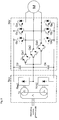
- Fig. 7 shows a circuit of a power conversion equipment (a three-level inverter) that outputs an alternating current voltage having three or more different potentials in a half-cycle period using IGBTs as semiconductor switching elements.
- a power conversion equipment a three-level inverter
- a direct current circuit portion of the three-level inverter has a configuration wherein it has a series circuit of capacitors Cp and Cn on a positive electrode side and negative electrode side as a direct current input, and a direct current power supply Ed is connected in parallel to the series circuit.
- an inverter INV has a configuration wherein each of bidirectional switches, wherein reverse blocking IGBTs are inverse parallel connected, is connected between alternating current terminals of a bridge circuit configured of six IGBTs (Qu, Qv, Qw, Qx, Qy, and Qz) and an internal connection point of the capacitor series circuit.
- a configuration is such that two direct current power supplies Ed1 and Ed2 are used in the direct current input portion, and connected in parallel to the series connected capacitors, and the inverter portion is the same as that in Fig. 7 .
- two direct current power supplies are necessary.
- the circuit configuration shown in Fig. 9 is an example of a heretofore known rectifying power supply wherein the two direct current power supplies Ed1 and Ed2 in the circuit of Fig. 8 are configured by a secondary two-winding transformer Tr1 and diode rectifier circuits Rec1 and Rec2.
- Fig. 10 is a voltage balancing chopper CH wherein a series circuit of semiconductor switching elements Qpch and Qnch is connected in parallel with the series circuit of the positive electrode side and negative electrode side capacitors, and a reactor Lch is connected between an internal connection point of the semiconductor switching elements Qpch and Qnch and an internal connection point of the capacitor series circuit.
- the semiconductor switching elements Qpch and Qnch are optionally turned on and off, thus adjusting the voltages.
- bidirectional switches are connected between a neutral point of a load and the internal connection point of the capacitor series circuit of the direct current input, and the bidirectional switches are optionally turned on and off in accordance with the difference between the capacitor voltages, thus adjusting a voltage unbalance.
- a power conversion equipment a capacitor series circuit in which a plurality of capacitors are connected in series being connected in parallel with a direct current power supply, outputs an alternating current voltage having three or more potentials in a half-cycle with the capacitor series circuit as a direct current input, wherein a neutral point of a star-connected alternating current load and an intermediate connection point of the capacitor series circuit are directly connected.
- the power conversion equipment according to the first aspect of the invention is preferably characterized in that the voltage of each of the capacitors is preferably detected, and/or a zero voltage vector obtained by making each alternating current output of the same potential is adjusted in accordance with the difference between the voltages.
- the voltage of each of the capacitors is preferably adjusted by controlling to a mode in which each alternating current output is of a neutral point potential.
- a power conversion equipment that can output an alternating current voltage having three or more different potentials in a half-cycle, it is possible to achieve the elimination of an unbalance in the voltages of positive electrode side and negative electrode side capacitors without adding separate parts, and a downsizing and reduction in cost of an equipment are possible.
- the essence of the invention lies in the point that in a power conversion equipment that, a capacitor series circuit in which a plurality of capacitors are connected in series being connected in parallel with a direct current power supply, outputs an alternating current voltage having three or more potentials in a half-cycle period with the capacitor series circuit as a direct current input, a neutral point of a star-connected alternating current load and an intermediate connection point of the capacitor series circuit are directly connected, the voltage of each of the capacitors is detected, and a zero voltage vector obtained by making each alternating current output of the same potential is adjusted in accordance with the difference between the voltages.
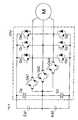
- Fig. 1 shows a first embodiment of the invention. It is a power conversion equipment (a three-level inverter) that can output an alternating current voltage having three or more different potentials in a half-cycle period using IGBTs as semiconductor switching elements.
- a direct current circuit portion of the three-level inverter has a configuration wherein it has a series circuit of capacitors Cp and Cn between a positive electrode and a negative electrode as a direct current input, and a direct current power supply Ed is connected in parallel to the series circuit.
- an inverter INV has a configuration wherein each of bidirectional switches Qsu, Qsv, and Qsw, wherein reverse blocking type IGBTs are inverse parallel connected, is connected between alternating current terminals of a bridge circuit configured of six IGBTs (Qu, Qv, Qw, Qx, Qy, and Qz) and an internal connection point of the capacitor series circuit. Also, a connection point of the capacitor series circuit of the capacitors Cp and Cn between the positive electrode and negative electrode, and a neutral point of a star-connected alternating current load M, are directly connected.
- voltage detectors Dp and Dn for detecting voltage are provided in the positive electrode side and negative electrode side capacitors Cp and Cn respectively, their outputs are level converted in a voltage detector circuit Dpt, the detected values thereof are sent to a PWM control circuit CONT, and on-off signals for the six IGBTs and three bidirectional switches are generated in the PWM control circuit CONT.
- FIG. 2A shows an equivalent circuit focused on a zero phase sequence component in the circuit configuration of Fig. 1 .
- a zero voltage is an alternating current output voltage when the IGBTs Qu, Qv, and Qw of the circuit of Fig. 1 are turned on simultaneously, or the IGBTs Qx, Qy, and Qz are turned on simultaneously, and it is possible, as shown in Fig. 2A , to replace with an equivalent circuit wherein the simultaneous turning on of the IGBTs Qu, Qv, and Qw is aggregated in an IGBT Qp, and the simultaneous turning on of the IGBTs Qx, Qy, and Qz in an IGBT Qn.
- the alternating current load M can be represented as an inductor Lz.
- the neutral point of the alternating current load M is connected to a connection point of direct current intermediate capacitors Cp and Cn, as previously described.
- FIG. 2B An operating example is shown in Figs. 2B and 2C . It is an operation when a charge of the capacitor Cp is moved to the capacitor Cn.
- the current flows along a path from the positive electrode side capacitor Cp, through the IGBT Qp, to the inductor Lz of the alternating current load M, and energy is accumulated in the inductor Lz of the alternating current load M.
- the energy accumulated in the inductor Lz of the alternating current load M charges the negative electrode side capacitor Cn via a diode inverse parallel connected to the IGBT Qn, as shown in Fig. 2C .
- the voltage of the capacitor Cp is high, it is possible, by means of this kind of operation, to move the charge of the capacitor Cp to the capacitor Cn.
- Figs. 3B and 3C show an operation when a charge of the capacitor Cn is moved to the capacitor Cp.
- the current flows along a path from the negative electrode side capacitor Cn, through the inductor Lz of the alternating current load M, to the IGBT Qn, and energy is accumulated in the inductor Lz of the alternating current load M.
- the energy accumulated in the inductor Lz of the alternating current load M charges the positive electrode side capacitor Cp via a diode inverse parallel connected to the IGBT Qp, as shown in Fig. 3C .
- Figs. 4A to 4C are diagrams illustrating the previously described operations based on a basic operational pattern of the three-level inverter.
- Fig. 4A shows the mode wherein the IGBT Qp is turned on, and energy is supplied from the positive electrode side capacitor Cp to the inductor Lz of the alternating current load M.
- the IGBT Qp being turned off, and a bidirectional switch Qs turned on, the energy accumulated in the inductor Lz of the alternating current load M flows back along a path passing through the alternating current switch Qs, as shown in Fig. 4B .
- the energy accumulated in the inductor Lz of the alternating current load M is accumulated in the negative electrode side capacitor Cn via the inverse parallel connected diode of the IGBT Qn, as shown in Fig. 4C .
- the transfer of a charge from the negative electrode side capacitor Cn to the positive electrode side capacitor Cp is also an inversely symmetrical operation, the same kind of operation is possible.
- the predetermined value refers to a capacitor voltage based on power which can be consumed by the resistance of the alternating current load M or bidirectional switch Qs.
- the predetermined value refers to a voltage based on power which can be consumed by the resistance of the alternating current load M, diodes D1 and D2, or IGBTs Q2 and Q3.
- Fig. 6 shows a third embodiment of the invention. It is an equivalent circuit focused on a zero phase sequence component showing an embodiment in a five-level inverter.
- a five-level inverter is a power conversion circuit that outputs an alternating current voltage having five potentials in a half-cycle period.
- a configuration is such that the two capacitors Cp and Cn of the direct current input of the inverter INV of the first embodiment shown in Fig. 1 are changed to four capacitors Cp1, Cp2, Cn1, and Cn2, and bidirectional switches are connected between connection points of the capacitors and alternating current outputs of the inverter. A neutral point of a load and an intermediate connection point of the series capacitor are connected. Operations in this kind of configuration are the same as those in the first embodiment.
- the series circuit of the capacitors Cp1 and Cp2 is a power supply
- a current flows along a path from the IGBT Qp, through the load M, to an intermediate connection point O of the four capacitors, and energy is accumulated in the inductor Lz of the load.
- the energy of the load enters a free wheeling mode on a bidirectional switch Qs2 being turned on, a mode charging the capacitor Cn1 on a bidirectional switch Qs3 being turned on, and a mode charging the capacitors Cn1 and Cn2 on the bidirectional switches Qs2 and Qs3 being left turned off.
- the capacitor Cp2 is a power supply, and energy is accumulated in the inductor Lz of the load.
- the energy of the load enters a free wheeling mode on the bidirectional switch Qs2 being turned on, a mode charging the capacitor Cn1 on a bidirectional switch Qs3 being turned on, and a mode charging the capacitors Cn1 and Cn2 on the bidirectional switches Qs2 and Qs3 being left turned off.
- the invention can be applied to a power conversion equipment that outputs an alternating current having three or more levels in a half-cycle period, regardless of a circuit configuration of the inverter.
- the invention can be applied to a motor drive equipment, an uninterruptible power supply system, or the like, to which is applied a multilevel inverter using a direct current input wherein which capacitors are connected in series.
Landscapes
- Engineering & Computer Science (AREA)
- Power Engineering (AREA)
- Inverter Devices (AREA)
- Ac-Ac Conversion (AREA)
- Rectifiers (AREA)
- Control Of Ac Motors In General (AREA)
Abstract
Description
- The present invention relates to a multilevel inverter that outputs an alternating current voltage having three or more different potentials in a half-cycle period, and in particular, relates to a technology for balancing the voltage of each capacitor in a capacitor series circuit installed in a direct current input.
-
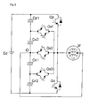
Fig. 7 shows a circuit of a power conversion equipment (a three-level inverter) that outputs an alternating current voltage having three or more different potentials in a half-cycle period using IGBTs as semiconductor switching elements. Although there are also configurations having more than three levels, such as five levels, as a multilevel inverter, a description will be given here with a three-level inverter as an example. A direct current circuit portion of the three-level inverter has a configuration wherein it has a series circuit of capacitors Cp and Cn on a positive electrode side and negative electrode side as a direct current input, and a direct current power supply Ed is connected in parallel to the series circuit. Also, an inverter INV has a configuration wherein each of bidirectional switches, wherein reverse blocking IGBTs are inverse parallel connected, is connected between alternating current terminals of a bridge circuit configured of six IGBTs (Qu, Qv, Qw, Qx, Qy, and Qz) and an internal connection point of the capacitor series circuit. - In the circuit configuration shown in
Fig. 8 , a configuration is such that two direct current power supplies Ed1 and Ed2 are used in the direct current input portion, and connected in parallel to the series connected capacitors, and the inverter portion is the same as that inFig. 7 . In the case of this configuration, two direct current power supplies are necessary.
The circuit configuration shown inFig. 9 is an example of a heretofore known rectifying power supply wherein the two direct current power supplies Ed1 and Ed2 in the circuit ofFig. 8 are configured by a secondary two-winding transformer Tr1 and diode rectifier circuits Rec1 and Rec2. By means of this configuration, it is possible to improve an alternating current power supply primary side power factor, while generating two direct current power supplies. However, in the event that the voltages of the positive electrode side and negative electrode side capacitors of the three-level inverter become unbalanced, the power factor worsens. - As heretofore described, various configurations are being employed for the direct current power supply portion of a three-level inverter that outputs an alternating current voltage having three potentials, in order to balance the voltages of the positive electrode side capacitor and negative electrode side capacitor. However, due to variations in IGBT operation and control, part variation, and the like, it is difficult to avert voltage unbalance with only the heretofore described circuit configurations.
- In order to solve this problem, the circuit configuration shown in
Fig. 10 and described in Japanese Patent No.3, 249, 380 Fig. 10 is a voltage balancing chopper CH wherein a series circuit of semiconductor switching elements Qpch and Qnch is connected in parallel with the series circuit of the positive electrode side and negative electrode side capacitors, and a reactor Lch is connected between an internal connection point of the semiconductor switching elements Qpch and Qnch and an internal connection point of the capacitor series circuit. When a difference occurs between the voltage values of the positive electrode side and negative electrode side capacitors Cp and Cn, the semiconductor switching elements Qpch and Qnch are optionally turned on and off, thus adjusting the voltages.
Also, according to Japanese Patent No.4,279,640 - As heretofore described, according to both Japanese Patent No.
3,249,380 4,279,640 - In order to solve the heretofore described problem, according to a first aspect of the invention, a power conversion equipment, a capacitor series circuit in which a plurality of capacitors are connected in series being connected in parallel with a direct current power supply, outputs an alternating current voltage having three or more potentials in a half-cycle with the capacitor series circuit as a direct current input, wherein a neutral point of a star-connected alternating current load and an intermediate connection point of the capacitor series circuit are directly connected.
- According to a second aspect of the invention, the power conversion equipment according to the first aspect of the invention is preferably characterized in that the voltage of each of the capacitors is preferably detected, and/or a zero voltage vector obtained by making each alternating current output of the same potential is adjusted in accordance with the difference between the voltages.
- According to a third aspect of the invention, when the difference between the detected voltage of each of the capacitors is smaller than a predetermined value, the voltage of each of the capacitors is preferably adjusted by controlling to a mode in which each alternating current output is of a neutral point potential.
- According to the invention, in a power conversion equipment that can output an alternating current voltage having three or more different potentials in a half-cycle, it is possible to achieve the elimination of an unbalance in the voltages of positive electrode side and negative electrode side capacitors without adding separate parts, and a downsizing and reduction in cost of an equipment are possible.
-
-
Fig. 1 shows a circuit configuration showing a first embodiment of the invention; -
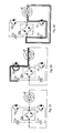
Figs. 2A to 2C are illustrations of a first operation in the first embodiment of the invention; -
Figs. 3A to 3C are illustrations of a second operation in the first embodiment of the invention; -
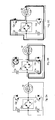
Figs. 4A to 4C are illustrations of a third operation in the first embodiment of the invention; -
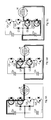
Figs. 5A to 5C are illustrations of an operation in a second embodiment of the invention; -
Fig. 6 is a circuit diagram showing a third embodiment of the invention; -
Fig. 7 is a circuit configuration diagram showing a first heretofore known example; -
Fig. 8 is a circuit configuration diagram showing a second heretofore known example; -
Fig. 9 is a circuit configuration diagram showing a specific example of the second heretofore known example; and -
Fig. 10 is a circuit configuration diagram showing a third heretofore known example; - The essence of the invention lies in the point that in a power conversion equipment that, a capacitor series circuit in which a plurality of capacitors are connected in series being connected in parallel with a direct current power supply, outputs an alternating current voltage having three or more potentials in a half-cycle period with the capacitor series circuit as a direct current input, a neutral point of a star-connected alternating current load and an intermediate connection point of the capacitor series circuit are directly connected, the voltage of each of the capacitors is detected, and a zero voltage vector obtained by making each alternating current output of the same potential is adjusted in accordance with the difference between the voltages.
-
Fig. 1 shows a first embodiment of the invention. It is a power conversion equipment (a three-level inverter) that can output an alternating current voltage having three or more different potentials in a half-cycle period using IGBTs as semiconductor switching elements. A direct current circuit portion of the three-level inverter has a configuration wherein it has a series circuit of capacitors Cp and Cn between a positive electrode and a negative electrode as a direct current input, and a direct current power supply Ed is connected in parallel to the series circuit. - Also, an inverter INV has a configuration wherein each of bidirectional switches Qsu, Qsv, and Qsw, wherein reverse blocking type IGBTs are inverse parallel connected, is connected between alternating current terminals of a bridge circuit configured of six IGBTs (Qu, Qv, Qw, Qx, Qy, and Qz) and an internal connection point of the capacitor series circuit. Also, a connection point of the capacitor series circuit of the capacitors Cp and Cn between the positive electrode and negative electrode, and a neutral point of a star-connected alternating current load M, are directly connected. Furthermore, voltage detectors Dp and Dn for detecting voltage are provided in the positive electrode side and negative electrode side capacitors Cp and Cn respectively, their outputs are level converted in a voltage detector circuit Dpt, the detected values thereof are sent to a PWM control circuit CONT, and on-off signals for the six IGBTs and three bidirectional switches are generated in the PWM control circuit CONT.
- A control operation in the PWM control circuit CONT is shown in
Figs. 2A to 2C. Fig. 2A shows an equivalent circuit focused on a zero phase sequence component in the circuit configuration ofFig. 1 . A zero voltage is an alternating current output voltage when the IGBTs Qu, Qv, and Qw of the circuit ofFig. 1 are turned on simultaneously, or the IGBTs Qx, Qy, and Qz are turned on simultaneously, and it is possible, as shown inFig. 2A , to replace with an equivalent circuit wherein the simultaneous turning on of the IGBTs Qu, Qv, and Qw is aggregated in an IGBT Qp, and the simultaneous turning on of the IGBTs Qx, Qy, and Qz in an IGBT Qn. Also, the alternating current load M can be represented as an inductor Lz. Furthermore, the neutral point of the alternating current load M is connected to a connection point of direct current intermediate capacitors Cp and Cn, as previously described. - Next, an operating example is shown in
Figs. 2B and 2C . It is an operation when a charge of the capacitor Cp is moved to the capacitor Cn. Firstly, inFig. 2B , on the IGBT Qp being turned on, the current flows along a path from the positive electrode side capacitor Cp, through the IGBT Qp, to the inductor Lz of the alternating current load M, and energy is accumulated in the inductor Lz of the alternating current load M. Next, on the IGBT Qp being turned off, the energy accumulated in the inductor Lz of the alternating current load M charges the negative electrode side capacitor Cn via a diode inverse parallel connected to the IGBT Qn, as shown inFig. 2C . When the voltage of the capacitor Cp is high, it is possible, by means of this kind of operation, to move the charge of the capacitor Cp to the capacitor Cn. -
Figs. 3B and 3C show an operation when a charge of the capacitor Cn is moved to the capacitor Cp. As shown inFig. 3B , on the IGBT Qn being turned on, the current flows along a path from the negative electrode side capacitor Cn, through the inductor Lz of the alternating current load M, to the IGBT Qn, and energy is accumulated in the inductor Lz of the alternating current load M. Next, on the IGBT Qn being turned off, the energy accumulated in the inductor Lz of the alternating current load M charges the positive electrode side capacitor Cp via a diode inverse parallel connected to the IGBT Qp, as shown inFig. 3C . When the voltage of the capacitor Cn is high, it is possible, by means of this kind of operation, to move the charge of the capacitor Cn to the capacitor Cp. By means of the heretofore described kinds of operation, it is possible to move the charge of the positive electrode side capacitor Cp to the negative electrode side capacitor Cn, or the charge of the negative electrode side capacitor Cn to the positive electrode side capacitor Cp. - That is, by detecting the voltages of the positive electrode side and negative electrode side capacitors Cp and Cn, and causing the operation of
Figs. 2B and 2C orFigs. 3B and 3C to be carried out in accordance with the voltage difference between their respective voltage values Vcp and Vcn, it is possible to equalize the voltages of the capacitors Cp and Cn. For example, by causing the operation ofFigs. 2B and 2C to be carried out when the voltage Vcp of the capacitor Cp is greater than the voltage Vcn of the capacitor Cn, and the operation ofFigs. 3B and 3C when the voltage Vcp of the capacitor Cp is smaller than the voltage Vcn of the capacitor Cn, it is possible to equalize the voltage values of the positive electrode side capacitor and negative electrode side capacitor, and it is possible to supply a stable power to the alternating current load M. -
Figs. 4A to 4C are diagrams illustrating the previously described operations based on a basic operational pattern of the three-level inverter.Fig. 4A shows the mode wherein the IGBT Qp is turned on, and energy is supplied from the positive electrode side capacitor Cp to the inductor Lz of the alternating current load M. Next, on the IGBT Qp being turned off, and a bidirectional switch Qs turned on, the energy accumulated in the inductor Lz of the alternating current load M flows back along a path passing through the alternating current switch Qs, as shown inFig. 4B . Next, on the bidirectional switch Qs being turned off, the energy accumulated in the inductor Lz of the alternating current load M is accumulated in the negative electrode side capacitor Cn via the inverse parallel connected diode of the IGBT Qn, as shown inFig. 4C . Also, as a transfer of a charge from the negative electrode side capacitor Cn to the positive electrode side capacitor Cp is also an inversely symmetrical operation, the same kind of operation is possible. - When the voltage difference between the positive electrode side capacitor and negative electrode side capacitor is smaller than a predetermined value, even when causing a current backflow, and causing consumption by utilizing resistance of the alternating current load M or bidirectional switch Qs, in the mode shown in
Fig. 4B , it is possible to balance the capacitor voltages. Consequently, the predetermined value refers to a capacitor voltage based on power which can be consumed by the resistance of the alternating current load M or bidirectional switch Qs. -
-
Figs. 5A to 5C show a second embodiment of the invention.Figs. 5A to 5C show a circuit configuration in a common neutral point clamping type three-level inverter using a clamping diode. Hereafter, operations will be described. -
Fig. 5A showing a mode wherein IGBTs Q1 and Q2 are turned on, and the alternating current load M is supplied from the positive side electrode capacitor Cp, energy is accumulated in the inductor Lz. Next, on the IGBT Q1 being turned off, and an IGBT Q3 turned on, the energy accumulated in the inductor Lz flows back via the IGBT Q2, as shown inFig. 5B . Next, on the IGBT Q2 being turned off, and an IGBT Q4 turned on, the energy accumulated in the alternating current load is accumulated in the negative electrode side capacitor Cn via a diode inverse parallel connected to the IGBTs Q3 and Q4. Also, as a transfer of energy from the negative electrode side capacitor Cn to the positive electrode side capacitor Cp is also an inversely symmetrical operation, the same kind of operation is possible. - When the voltage difference between the positive electrode side capacitor and negative electrode side capacitor is smaller than a predetermined value, even when causing a current backflow, and causing consumption by utilizing resistance of the alternating current load M, diodes D1 and D2, and IGBTs Q2 and Q3, in the mode shown in
Fig. 5B , it is possible to balance the capacitor voltages. Consequently, the predetermined value refers to a voltage based on power which can be consumed by the resistance of the alternating current load M, diodes D1 and D2, or IGBTs Q2 and Q3. -
Fig. 6 shows a third embodiment of the invention. It is an equivalent circuit focused on a zero phase sequence component showing an embodiment in a five-level inverter. A five-level inverter is a power conversion circuit that outputs an alternating current voltage having five potentials in a half-cycle period. A configuration is such that the two capacitors Cp and Cn of the direct current input of the inverter INV of the first embodiment shown inFig. 1 are changed to four capacitors Cp1, Cp2, Cn1, and Cn2, and bidirectional switches are connected between connection points of the capacitors and alternating current outputs of the inverter. A neutral point of a load and an intermediate connection point of the series capacitor are connected.
Operations in this kind of configuration are the same as those in the first embodiment. - In a mode in which the IGBT Qp is turned on and off, on the IGBT Qp being turned on, the series circuit of the capacitors Cp1 and Cp2 is a power supply, a current flows along a path from the IGBT Qp, through the load M, to an intermediate connection point O of the four capacitors, and energy is accumulated in the inductor Lz of the load. Next, on the IGBT Qp being turned off, the energy of the load enters a free wheeling mode on a bidirectional switch Qs2 being turned on, a mode charging the capacitor Cn1 on a bidirectional switch Qs3 being turned on, and a mode charging the capacitors Cn1 and Cn2 on the bidirectional switches Qs2 and Qs3 being left turned off.
- In a mode in which a bidirectional switch Qs1 is turned on and off, on the bidirectional switch Qs1 being turned on, the capacitor Cp2 is a power supply, and energy is accumulated in the inductor Lz of the load. Next, on the bidirectional switch Qs1 being turned off, the energy of the load enters a free wheeling mode on the bidirectional switch Qs2 being turned on, a mode charging the capacitor Cn1 on a bidirectional switch Qs3 being turned on, and a mode charging the capacitors Cn1 and Cn2 on the bidirectional switches Qs2 and Qs3 being left turned off.
Also, as a transfer of energy from the negative electrode side capacitors Cn1 and Cn2 to the positive electrode side capacitors Cp1 and Cp2 is also an inversely symmetrical operation, the same kind of operation is possible.
Also, when the voltage difference between the capacitors is smaller than a predetermined value, it is possible to cause energy to be consumed by means of the free wheeling mode.
By means of the heretofore described kinds of operation, it is possible to move a charge from a capacitor with a higher voltage to a capacitor with a lower voltage, and it is possible to balance the capacitor voltages.
Although examples in a three-level and five-level inverter have been shown in the embodiments, the invention can be applied to a power conversion equipment that outputs an alternating current having three or more levels in a half-cycle period, regardless of a circuit configuration of the inverter. - The invention can be applied to a motor drive equipment, an uninterruptible power supply system, or the like, to which is applied a multilevel inverter using a direct current input wherein which capacitors are connected in series.
Features, components and specific details of the structures of the above-described embodiments may be exchanged or combined to form further embodiments optimized for the respective application. As far as those modifications are readily apparent for an expert skilled in the art they shall be disclosed implicitly by the above description without specifying explicitly every possible combination, for the sake of conciseness of the present description.
Claims (3)
- A power conversion equipment that, a capacitor series circuit in which a plurality of capacitors (Cp, Cn) are connected in series being connected in parallel with a direct current power supply (Ed), outputs an alternating current voltage having three or more potentials in a half-cycle with the capacitor series circuit as a direct current input, wherein
a neutral point of a star-connected alternating current load (M) and an intermediate connection point of the capacitor series circuit are directly connected. - The power conversion equipment according to claim 1, wherein
the voltage of each of the capacitors (Cp, Cn) is detected, and a zero voltage vector obtained by making each alternating current output of the same potential is adjusted in accordance with the difference between the voltages. - The power conversion equipment according to claim 1 or 2, wherein
when the difference between the detected voltage of each of the capacitors (Cp, Cn) is smaller than a predetermined value, the voltage of each of the capacitors (Cp, Cn) is adjusted by controlling to a mode in which each alternating current output is of a neutral point potential.
Applications Claiming Priority (1)
| Application Number | Priority Date | Filing Date | Title |
|---|---|---|---|
| JP2009261501A JP2011109789A (en) | 2009-11-17 | 2009-11-17 | Power converter |
Publications (2)
| Publication Number | Publication Date |
|---|---|
| EP2325994A2 true EP2325994A2 (en) | 2011-05-25 |
| EP2325994A3 EP2325994A3 (en) | 2011-07-06 |
Family
ID=43858161
Family Applications (1)
| Application Number | Title | Priority Date | Filing Date |
|---|---|---|---|
| EP10189050A Withdrawn EP2325994A3 (en) | 2009-11-17 | 2010-10-27 | Power conversion equipment |
Country Status (4)
| Country | Link |
|---|---|
| US (1) | US20110116293A1 (en) |
| EP (1) | EP2325994A3 (en) |
| JP (1) | JP2011109789A (en) |
| CN (1) | CN102075105A (en) |
Cited By (3)
| Publication number | Priority date | Publication date | Assignee | Title |
|---|---|---|---|---|
| EP2811629A2 (en) * | 2013-06-05 | 2014-12-10 | LSIS Co., Ltd. | Multilevel inverter |
| EP2936671A4 (en) * | 2012-12-19 | 2016-08-24 | Comsys Ab | Auxiliary resonant commutated pole converter with voltage balancing circuit |
| EP3382874A1 (en) * | 2017-03-31 | 2018-10-03 | Schneider Electric IT Corporation | Bi-directional dc-dc converter with load and source synchronized power control |
Families Citing this family (35)
| Publication number | Priority date | Publication date | Assignee | Title |
|---|---|---|---|---|
| CN102255538B (en) * | 2010-05-19 | 2014-03-12 | 力博特公司 | T-shaped three-level inverter circuit |
| WO2012169521A1 (en) | 2011-06-10 | 2012-12-13 | 富士電機株式会社 | Semiconductor module, upper and lower arm kit and three-level inverter |
| DE102011115728B4 (en) | 2011-10-12 | 2022-11-17 | Sew-Eurodrive Gmbh & Co Kg | Method of operating an inverter and inverter circuit |
| US20140362626A1 (en) * | 2011-12-28 | 2014-12-11 | Panasonic Corporation | Multilevel inverter device |
| WO2013114688A1 (en) * | 2012-02-02 | 2013-08-08 | 三菱電機株式会社 | Device for controlling alternating current rotating machine |
| CN110022078B (en) * | 2012-03-30 | 2021-05-04 | 富士电机株式会社 | power conversion device |
| US9413268B2 (en) * | 2012-05-10 | 2016-08-09 | Futurewei Technologies, Inc. | Multilevel inverter device and method |
| US9214874B2 (en) * | 2012-07-31 | 2015-12-15 | Yashomani Y. Kolhatkar | Intelligent level transition systems and methods for transformerless uninterruptible power supply |
| JP6011197B2 (en) * | 2012-09-24 | 2016-10-19 | 株式会社明電舎 | Multi-level power converter |
| CN104756397B (en) * | 2012-11-09 | 2017-08-25 | 本田技研工业株式会社 | Supply unit |
| EP2919377B1 (en) * | 2012-11-09 | 2018-10-31 | Fuji Electric Co., Ltd. | Inverter device |
| CN103023363B (en) * | 2012-11-26 | 2015-04-08 | 华为技术有限公司 | Five-level inverter |
| CN103178736B (en) * | 2013-03-22 | 2015-07-29 | 阳光电源股份有限公司 | A kind of five-electrical level inverter |
| WO2014194933A1 (en) * | 2013-06-04 | 2014-12-11 | Huawei Technologies Co., Ltd. | Five-level pv inverter based on a multi-state switching cell |
| US9799731B2 (en) * | 2013-06-24 | 2017-10-24 | Ideal Power, Inc. | Multi-level inverters using sequenced drive of double-base bidirectional bipolar transistors |
| JP6086832B2 (en) * | 2013-07-10 | 2017-03-01 | 新電元工業株式会社 | Inverter circuit |
| JP6086157B2 (en) * | 2013-10-02 | 2017-03-01 | 富士電機株式会社 | 3-level inverter |
| KR102166362B1 (en) | 2013-12-18 | 2020-10-15 | 오티스 엘리베이터 컴파니 | Bus capacitor bank configuration for a multi-level regenerative drive |
| DE102014224371A1 (en) * | 2014-11-28 | 2016-06-02 | Robert Bosch Gmbh | Battery system with a hybrid battery and an NPC inverter connected to the battery on the input side and method for operating an NPC inverter connected on the input side with a hybrid battery |
| CN104410307B (en) * | 2014-12-18 | 2017-01-18 | 阳光电源股份有限公司 | Working mode switching method and device for five-level inverter |
| BR112017027795B1 (en) * | 2015-06-23 | 2022-10-04 | Nissan Motor Co., Ltd | INVERTER WITH LOADING CAPACITY |
| CN105391330B (en) * | 2015-12-22 | 2018-05-25 | 阳光电源股份有限公司 | A kind of three-level inverter and its busbar voltage balance control method and control device |
| CN106253724B (en) * | 2016-08-10 | 2019-07-26 | 全球能源互联网研究院有限公司 | A kind of current transformer |
| US10211672B2 (en) * | 2016-10-13 | 2019-02-19 | Schneider Electric It Corporation | DC-link bus balancer |
| JP2018085858A (en) * | 2016-11-24 | 2018-05-31 | 富士電機株式会社 | Power converter |
| US10812014B1 (en) * | 2018-04-05 | 2020-10-20 | The Regents Of The University Of Colorado | Modular photovoltaic string inverter system adapted for SiC MOSFETs |
| DE102018120236A1 (en) * | 2018-08-20 | 2020-02-20 | Thyssenkrupp Ag | Charging device with controllable intermediate circuit center voltage and drive system with such a charging device |
| DE102018124789A1 (en) * | 2018-10-08 | 2020-04-09 | Thyssenkrupp Ag | Fast charging device and electric drive system with such a quick charging device |
| DE102018124787A1 (en) * | 2018-10-08 | 2020-04-09 | Thyssenkrupp Ag | Charging device and electric drive system with such a charging device |
| US11329578B2 (en) * | 2019-08-08 | 2022-05-10 | Lg Electronics Inc. | Device for driving a plurality of motors and electric apparatus including the same |
| CN112838773A (en) * | 2019-11-25 | 2021-05-25 | 开利公司 | Power Modules and Converters with Asymmetric Semiconductor Rating Arrangements |
| CN114337332B (en) | 2020-09-30 | 2023-12-22 | 重庆美的制冷设备有限公司 | Three-phase power supply conversion circuit, circuit control method, circuit board and air conditioner |
| JP7607323B2 (en) * | 2021-02-26 | 2024-12-27 | 学校法人大阪産業大学 | High power factor rectifier circuit |
| JP7760922B2 (en) * | 2022-01-28 | 2025-10-28 | 富士電機株式会社 | Power Conversion Device |
| WO2023181368A1 (en) * | 2022-03-25 | 2023-09-28 | 三菱電機株式会社 | Power converter |
Citations (2)
| Publication number | Priority date | Publication date | Assignee | Title |
|---|---|---|---|---|
| JP3249380B2 (en) | 1995-06-13 | 2002-01-21 | 株式会社東芝 | Power converter |
| JP4279640B2 (en) | 2003-09-26 | 2009-06-17 | 東芝三菱電機産業システム株式会社 | Power converter |
Family Cites Families (6)
| Publication number | Priority date | Publication date | Assignee | Title |
|---|---|---|---|---|
| JPS58112476A (en) * | 1981-12-25 | 1983-07-04 | Toyota Central Res & Dev Lab Inc | multilevel inverter |
| DE3415145A1 (en) * | 1984-04-21 | 1985-10-31 | Mitec Moderne Ind Gmbh | INVERTER |
| JP3170838B2 (en) * | 1992-01-28 | 2001-05-28 | ブラザー工業株式会社 | Drive device for variable reluctance motor |
| JP3223842B2 (en) * | 1997-06-03 | 2001-10-29 | 富士電機株式会社 | Multi-phase output power conversion circuit |
| JP4575555B2 (en) * | 2000-06-30 | 2010-11-04 | トヨタ自動車株式会社 | Power output device |
| EP1861914B1 (en) * | 2005-10-24 | 2008-12-03 | Conergy AG | Inverter |
-
2009
- 2009-11-17 JP JP2009261501A patent/JP2011109789A/en not_active Withdrawn
-
2010
- 2010-10-27 EP EP10189050A patent/EP2325994A3/en not_active Withdrawn
- 2010-11-15 CN CN2010105559381A patent/CN102075105A/en active Pending
- 2010-11-16 US US12/947,541 patent/US20110116293A1/en not_active Abandoned
Patent Citations (2)
| Publication number | Priority date | Publication date | Assignee | Title |
|---|---|---|---|---|
| JP3249380B2 (en) | 1995-06-13 | 2002-01-21 | 株式会社東芝 | Power converter |
| JP4279640B2 (en) | 2003-09-26 | 2009-06-17 | 東芝三菱電機産業システム株式会社 | Power converter |
Cited By (6)
| Publication number | Priority date | Publication date | Assignee | Title |
|---|---|---|---|---|
| EP2936671A4 (en) * | 2012-12-19 | 2016-08-24 | Comsys Ab | Auxiliary resonant commutated pole converter with voltage balancing circuit |
| EP2811629A2 (en) * | 2013-06-05 | 2014-12-10 | LSIS Co., Ltd. | Multilevel inverter |
| EP3382874A1 (en) * | 2017-03-31 | 2018-10-03 | Schneider Electric IT Corporation | Bi-directional dc-dc converter with load and source synchronized power control |
| CN108696146A (en) * | 2017-03-31 | 2018-10-23 | 施耐德电气It公司 | With the bidirectional DC-DC converter for loading the Electric control synchronous with source |
| US10811987B2 (en) | 2017-03-31 | 2020-10-20 | Schneider Electric It Corporation | Bi-directional DC-DC converter with load and source synchronized power control |
| CN108696146B (en) * | 2017-03-31 | 2020-12-01 | 施耐德电气It公司 | Bidirectional DC-DC converter with load and source synchronous power control |
Also Published As
| Publication number | Publication date |
|---|---|
| JP2011109789A (en) | 2011-06-02 |
| US20110116293A1 (en) | 2011-05-19 |
| CN102075105A (en) | 2011-05-25 |
| EP2325994A3 (en) | 2011-07-06 |
Similar Documents
| Publication | Publication Date | Title |
|---|---|---|
| US20110116293A1 (en) | Power conversion equipment | |
| US9660482B2 (en) | Power conversion device with momentary voltage drop compensation | |
| US9325252B2 (en) | Multilevel converter systems and sinusoidal pulse width modulation methods | |
| US8233300B2 (en) | Device for converting an electric current | |
| JP5269102B2 (en) | Power converter | |
| JP5400961B2 (en) | Power converter | |
| US10177682B2 (en) | Switching unit for a converter module for a multi-level energy converter | |
| CN101128973A (en) | power conversion device | |
| JP5939411B2 (en) | Power converter | |
| RU2649888C2 (en) | Assembly for compensating reactive power and active power in a high-voltage network | |
| WO2013136378A1 (en) | Power conversion apparatus | |
| JP2008022625A (en) | AC-DC converter | |
| EP2677654B1 (en) | Inverter circuit | |
| JP5971685B2 (en) | Power converter | |
| JP5734083B2 (en) | Power converter | |
| JP2004180422A (en) | PWM rectifier | |
| Yalla et al. | A new three-phase multipoint clamped 5L-HPFC with reduced PSD count and switch stress | |
| JP2015015778A (en) | Power conversion system for system interconnection | |
| JP5400955B2 (en) | Power converter | |
| JP5752580B2 (en) | Power converter | |
| JP2020010564A (en) | Power converter | |
| JP2003018851A (en) | Control method of direct frequency conversion circuit | |
| JP2023050505A (en) | power converter |
Legal Events
| Date | Code | Title | Description |
|---|---|---|---|
| PUAI | Public reference made under article 153(3) epc to a published international application that has entered the european phase |
Free format text: ORIGINAL CODE: 0009012 |
|
| AK | Designated contracting states |
Kind code of ref document: A2 Designated state(s): AL AT BE BG CH CY CZ DE DK EE ES FI FR GB GR HR HU IE IS IT LI LT LU LV MC MK MT NL NO PL PT RO RS SE SI SK SM TR |
|
| AX | Request for extension of the european patent |
Extension state: BA ME |
|
| PUAL | Search report despatched |
Free format text: ORIGINAL CODE: 0009013 |
|
| AK | Designated contracting states |
Kind code of ref document: A3 Designated state(s): AL AT BE BG CH CY CZ DE DK EE ES FI FR GB GR HR HU IE IS IT LI LT LU LV MC MK MT NL NO PL PT RO RS SE SI SK SM TR |
|
| AX | Request for extension of the european patent |
Extension state: BA ME |
|
| RAP1 | Party data changed (applicant data changed or rights of an application transferred) |
Owner name: FUJI ELECTRIC CO., LTD. |
|
| STAA | Information on the status of an ep patent application or granted ep patent |
Free format text: STATUS: THE APPLICATION IS DEEMED TO BE WITHDRAWN |
|
| 18D | Application deemed to be withdrawn |
Effective date: 20120110 |