EP2323255A1 - Circuit d'amplification de puissance d'un signal d'entrée et système d'émission incorporant un tel circuit - Google Patents
Circuit d'amplification de puissance d'un signal d'entrée et système d'émission incorporant un tel circuit Download PDFInfo
- Publication number
- EP2323255A1 EP2323255A1 EP10190278A EP10190278A EP2323255A1 EP 2323255 A1 EP2323255 A1 EP 2323255A1 EP 10190278 A EP10190278 A EP 10190278A EP 10190278 A EP10190278 A EP 10190278A EP 2323255 A1 EP2323255 A1 EP 2323255A1
- Authority
- EP
- European Patent Office
- Prior art keywords
- transistor
- input
- main
- circuit
- auxiliary
- Prior art date
- Legal status (The legal status is an assumption and is not a legal conclusion. Google has not performed a legal analysis and makes no representation as to the accuracy of the status listed.)
- Granted
Links
Images
Classifications
-
- H—ELECTRICITY
- H03—ELECTRONIC CIRCUITRY
- H03F—AMPLIFIERS
- H03F3/00—Amplifiers with only discharge tubes or only semiconductor devices as amplifying elements
- H03F3/189—High-frequency amplifiers, e.g. radio frequency amplifiers
- H03F3/19—High-frequency amplifiers, e.g. radio frequency amplifiers with semiconductor devices only
- H03F3/191—Tuned amplifiers
-
- H—ELECTRICITY
- H03—ELECTRONIC CIRCUITRY
- H03F—AMPLIFIERS
- H03F1/00—Details of amplifiers with only discharge tubes, only semiconductor devices or only unspecified devices as amplifying elements
- H03F1/30—Modifications of amplifiers to reduce influence of variations of temperature or supply voltage or other physical parameters
- H03F1/302—Modifications of amplifiers to reduce influence of variations of temperature or supply voltage or other physical parameters in bipolar transistor amplifiers
-
- H—ELECTRICITY
- H03—ELECTRONIC CIRCUITRY
- H03F—AMPLIFIERS
- H03F3/00—Amplifiers with only discharge tubes or only semiconductor devices as amplifying elements
- H03F3/30—Single-ended push-pull [SEPP] amplifiers; Phase-splitters therefor
- H03F3/3083—Single-ended push-pull [SEPP] amplifiers; Phase-splitters therefor the power transistors being of the same type
- H03F3/3086—Single-ended push-pull [SEPP] amplifiers; Phase-splitters therefor the power transistors being of the same type two power transistors being controlled by the input signal
Definitions
- the invention relates to a power amplification circuit, in particular made on silicon and capable of processing signals whose frequency is in the X band (typically between 8 and 12 GHz).
- These circuits can for example be used in active transmit / receive modules, such as those integrated within the radars. More specifically, these modules include chips capable of phase shifting and attenuating or amplifying the signal received or to be transmitted.
- the amplification function is performed by the amplification circuit which ideally must be able to provide the necessary power required while ensuring good linearity of the transmission / reception chain.
- the amplification circuit is defined in particular by its input impedance, its gain and its transition frequency.
- the fact of working at high gain values implies a low input impedance, in particular related to the use of a transistor that is self-biased by a current source, (for example a current mirror) and mounted as a common emitter.
- a current source for example a current mirror
- An object of the invention is notably to solve these problems.
- the first main input transistor is coupled to the output stage via a second main input transistor, incorporated in the input stage and controlled by the control means, the first and second main input transistors being coupled to each other and to the ground in a Darlington type structure via a resonant circuit.
- the structure of the self-biased transistor is notably replaced by a Darlington type structure.
- the invention thus makes it possible to increase the value of the input impedance of the circuit, and consequently the value of the transition frequency.
- the linear operating range is thus increased.
- the amplification circuit is able to process signals whose frequency is in the X band.
- the first and second main input transistor can be configured to be traversed by currents of equivalent amplitude, with one error.
- said input signal may be of simple type, said second main transistor then being controlled by the main driving transistor.
- each said auxiliary element being mounted symmetrically to the corresponding element said principal.
- the second main input transistor can be controlled by the main drive transistor, and the second auxiliary input transistor can be controlled by the auxiliary drive transistor.
- the second main input transistor may be controlled by the auxiliary drive transistor, and the second auxiliary input transistor be controlled by the main drive transistor.
- the first and second auxiliary input transistor can be configured to be traversed by currents of equivalent amplitude, with one error.
- the circuit can be made in addition to silicon.
- a system for transmitting / transmitting a signal incorporating a circuit as mentioned above.
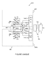
- the reference CIR designates an amplification circuit.
- This comprises an input stage EE coupled to an output stage ES.
- the input stage is here formed by two symmetrical branches BR and BRS coupled together via two coils BB1 and BB2, as described in more detail below.
- the CIR circuit has two branches BR and BRS because we consider a differential type input signal. In the case of a simple type input signal, the CIR circuit would naturally be formed of only one of the two branches.
- the branch BR will be described in detail. To each element said principal of the section BR corresponds a symmetrical auxiliary element said within the branch BRS.
- the references of these auxiliary elements include a suffix "s" as shown in the figure. In order to simplify the description, only the BR branch will be described, the BRS branch being similar to it.
- a bias current Ip is supplied at the input of the input stage EE, both on the branch BR and on the branch BRS, since a differential type input signal is considered.
- the differential input signal is applied in the form of a differential voltage VeVes, respectively on the input terminals En and Ens of the branches BR and BRS of the CIR circuit. More specifically, the input differential voltage is applied to the respective base of a first main transistor T1 and a first auxiliary transistor, T1 s via two capacitors referenced Cp and Cps.
- the bias current Ip is delivered at the input of a main bias transistor T3, more precisely on its collector.
- the main bias transistor T3 is mounted in current mirror with the first main transistor T1.
- the base of the main bias transistor T3 is connected to the base of the first main transistor T1, here via two resistors Ra and Rb connected in series.
- Their respective value may be of the order of one hundred ohms.
- a transistor T4 is also connected between the current source delivering the bias current Ip and the node common to the two resistors Ra and Rb.
- This transistor supplies an additional base current, the value of which corresponds to the value of the current dissipated by the main bias transistor T3.
- the emitter of the main bias transistor T3 is connected via a coil BB1 to the emitter of the auxiliary bias transistor T3s.
- the two transistors T3 and T3s form a control means MP.
- the emitter of the first main input transistor T1 is connected via a coil BB2 to the emitter of the first input auxiliary transistor T1 s.
- These coils BB1 and BB2 make it possible to decouple the transistors T3, T3s, T1 and T1s from the ground, by creating a high impedance at the working frequency.
- the coil BB2 forms a resonant circuit of the LC type with the capacitor Cp, this resonant circuit coupling the transistors T1 and T2 with each other and with the mass symbolized by a white arrow.
- This resonant circuit allows the amplification circuit to be able to process signals whose frequency is in the X band.
- the first main input transistor T1 is mounted according to a Darlington type structure well known to those skilled in the art with a second main input transistor T2.
- the collector of the second main input transistor T2 is coupled to the collector of the first main input transistor T1.
- the base of the second main input transistor T2 is coupled to the emitter of the first input main transistor T1 via a capacitor Cp.
- the first and second main input transistors are configured to be traversed by currents of similar values, with one error.
- Equation (2) The input impedance according to the invention (equation (2)) is thus much greater than the input impedance of the circuits according to the prior art (see equation (1) above), improving the coupling with a possible circuit coupled upstream.
- the extent of the linear operating zone of the CIR circuit is greatly increased. As a result, it is possible to benefit from the maximum value of the gain of the circuit for a wider range of frequencies.
- the base of the second main input transistor T2 is connected to the base of the auxiliary bias transistor T3s.
- the transistor is driven in dynamic mode by the first main input transistor T1.
- the second main input transistor T2 is biased by the main bias transistor T3s.
- the base of the second main input transistor T2 may be connected to the base of the main bias transistor T3 and the base of the second input auxiliary transistor T2s connected to the base of the auxiliary bias transistor T3 (as shown in FIG. the figure).
- the cross illustrated in the figure allows to reflect the variations of a branch within the other branch and thus maintain a perfectly symmetrical differential signal.
- the second main input transistor T2 is cascode-mounted with a transistor T5.
- the emitter of the second main input transistor T2 is connected to ground and its collector is coupled to the emitter of transistor T5.
- the base of the transmitter T5 is connected to a reference voltage terminal Vref.
- the collector of the transistor T5 is coupled to the output stage ES.
- the latter comprises for this differential mode a balun BL that is to say an electrical circuit capable of making the connection between parallel printed lines and a printed line above a ground plane.
- the balun BL is powered by a supply voltage Vcc, and the output voltage between an output terminal St of the CIR circuit and the ground is referenced St.
- the supply voltage Vcc is also used to supply all the active elements of the CIR circuit.
- the connections are not shown for reasons of simplification.
- the amplification circuit CIR according to the invention also has the advantage of being particularly compact. Indeed, the transistor T3 (or T3s according to the chosen configuration) directly participating in the static polarization of the transistor T2 (or T2s), it is particularly advantageous for the place near T2 transistors (or T2s). The result is a space-saving circuit.
- the transistors used in this example are of the bipolar type on a silicon substrate. It is also possible to use bipolar transistors on AsGa or InP type substrate.
Landscapes
- Engineering & Computer Science (AREA)
- Power Engineering (AREA)
- Amplifiers (AREA)
Abstract
Description
- L'invention porte sur un circuit d'amplification de puissance, en particulier réalisé sur silicium et apte à traiter des signaux dont la fréquence est comprise dans la bande X (classiquement, entre 8 et 12 GHz).
- Ces circuits peuvent être par exemple utilisés dans des modules actifs d'émission/réception, tel que ceux intégrés au sein des radars. Plus précisément, ces modules comprennent des puces aptes à déphaser et atténuer ou amplifier le signal reçu ou à émettre. La fonction d'amplification est réalisée par le circuit d'amplification qui idéalement doit être capable de fournir la puissance nécessaire requise tout en garantissant une bonne linéarité de la chaîne d'émission/réception.
- Un circuit d'amplification idéal doit notamment :
- fournir le niveau puissance requis en sortie,
- perturber le moins possible les autres circuits couplés en amont,
- être suffisamment linéaire pour les applications visées, et
- permettre le contrôle du gain de sortie,
- Le circuit d'amplification est notamment défini par son impédance d'entrée, son gain et sa fréquence de transition.
- De façon que le fonctionnement du circuit soit optimal, il est préférable de se placer dans sa zone de fonctionnement linéaire, de façon à bénéficier de valeurs maximales et contrôlées du gain d'amplification.
- Cette zone de fonctionnement linaire est formée par les fréquences comprises entre 0 et la fréquence de transition Ft. Cette dernière est définie par :
- où :
- Ft est la fréquence de transition,
- Fc la fréquence de coupure, et
- Gmax, la valeur maximale pouvant être prise par le gain en courant du circuit d'amplification.
- Pour pouvoir délivrer de sortie maximale, il est nécessaire de se placer à des valeurs de fréquence pour lesquelles le gain prend sa valeur maximale, c'est-à-dire dans la zone de fonctionnement linéaire du circuit.
- Or jusque lors, dans les circuits d'amplification, le fait de travailler à des valeurs de gain élevées implique une impédance d'entrée faible, notamment lié à l'utilisation d'un transistor autopolarisé par une source de courant, (par exemple un miroir de courant) et monté en émetteur commun.
- Dans cette configuration (pour des transistors de dimensions judicieusement choisies), l'impédance d'entrée s'exprime sous la forme :

où : - Ze est l'impédance d'entrée du circuit d'amplification, et
- β est le gain du transistor autopolarisé.
- Une impédance d'entrée faible a pour désavantage :
- d'être néfaste au couplage avec un autre circuit disposé en amont, et
- de diminuer la valeur de la fréquence de transition, et par conséquent de réduire l'étendue de la zone de fonctionnement linaire du circuit d'amplification.
- Un but de l'invention est notamment de résoudre ces problèmes.
- A cet effet, selon un premier aspect de l'invention, il est proposé un circuit d'amplification de puissance d'un signal d'entrée comprenant un étage d'entrée et un étage de sortie, ledit étage d'entrée comportant :
- un moyen de pilotage incorporant un transistor de pilotage dit principal, et
- un premier transistor d'entrée dit principal apte à recevoir le signal d'entrée, et monté en miroir de courant avec le transistor de pilotage principal.
- Selon un caractéristique générale de cet aspect, le premier transistor d'entrée principal est couplé à l'étage de sortie via un deuxième transistor d'entrée dit principal, incorporé à l'étage d'entrée et commandé par le moyen de pilotage, les premier et deuxième transistors d'entrée principaux étant couplés entre eux et avec la masse selon une structure de type Darlington par l'intermédiaire d'un circuit résonnant.
- En d'autres termes, tout en conservant la fonction amplificatrice du circuit, la structure du transistor auto-polarisé est notamment remplacée par une structure de type Darlington.
- L'invention permet ainsi d'augmenter la valeur de l'impédance d'entrée du circuit, et par voie de conséquence, celle de la fréquence de transition. La plage de fonctionnement linaire en est ainsi accrue.
- Par ailleurs, de par l'utilisation d'un circuit résonnant pour le couplage des premier et deuxième transistors principaux, le circuit d'amplification est apte à traiter des signaux dont la fréquence est comprise dans la bande X.
- Selon un mode de réalisation, le premier et le deuxième transistor d'entrée principal peuvent être configurés de façon à être traversés par des courants d'amplitude équivalente, à une erreur près.
- Par exemple ledit signal d'entrée peut être de type simple, ledit deuxième transistor principal étant alors commandé par le transistor de pilotage principal.
- En variante, ledit signal d'entrée est de type différentiel, l'étage d'entrée comprenant alors en outre :
- un transistor de pilotage dit auxiliaire, incorporé au sein dudit moyen de pilotage,
- un premier transistor d'entrée dit auxiliaire, et
- un deuxième transistor d'entrée dit auxiliaire,
- chaque élément dit auxiliaire étant monté symétriquement à l'élément correspondant dit principal.
- Selon un mode de réalisation, le deuxième transistor d'entrée principal peut être commandé par le transistor de pilotage principal, et le deuxième transistor d'entrée auxiliaire être commandé par le transistor de pilotage auxiliaire.
- En variante, le deuxième transistor d'entrée principal peut être commandé par le transistor de pilotage auxiliaire, et le deuxième transistor d'entrée auxiliaire être commandé par le transistor de pilotage principal.
- De préférence, le premier et le deuxième transistor d'entrée auxiliaires peuvent être configurés de façon à être traversés par des courants d'amplitude équivalente, à une erreur près.
- Selon un mode de réalisation, le circuit peut être réalisé en outre sur silicium.
- Selon un autre aspect de l'invention, il est proposé un système d'émission/transmission d'un signal, incorporant un circuit tel que mentionné ci-avant.
- Selon un autre aspect de l'invention, il est proposé une utilisation d'un système d'émission/transmission d'un signal mentionné ci-dessus, au sein d'un radar.
- D'autres avantages et caractéristiques de l'invention apparaîtront à l'examen de la description détaillée d'un mode de réalisation selon l'invention, nullement limitatif, et d'une figure unique annexée sur laquelle est représenté un exemple de circuit d'amplification selon l'invention.
- On se réfère à présent à la figure unique. La référence CIR désigne un circuit d'amplification.
- Celui-ci comprend un étage d'entrée EE couplé à un étage de sortie ES.
- L'étage d'entrée est ici formé de deux branches symétriques BR et BRS couplées entre-elles via deux bobines BB1 et BB2, comme décrit plus en détail ci-après.
- Le circuit CIR comporte deux branches BR et BRS car l'on considère un signal d'entrée de type différentiel. Dans le cas d'un signal d'entrée de type simple, le circuit CIR ne serait naturellement formé que d'une seule des deux branches.
- La branche BR va être décrite de manière détaillée. A chaque élément dit principal de la banche BR correspond un élément dit auxiliaire symétrique au sein de la branche BRS. Les références de ces éléments auxiliaires comportent un suffixe « s », comme représenté sur la figure. De façon à simplifier la description, seule la branche BR va être décrite, la branche BRS lui étant similaire.
- Un courant de polarisation Ip est délivré en entrée de l'étage d'entrée EE, à la fois sur la branche BR et sur la branche BRS, étant donné que l'on considère un signal d'entrée de type différentiel.
- Le signal d'entrée différentiel est appliqué sous forme d'une tension différentielle VeVes, respectivement sur les bornes d'entrée En et Ens des branches BR et BRS du circuit CIR. Plus précisément, la tension différentielle d'entrée est appliquée sur la base respective d'un premier transistor principal T1 et d'un premier transistor auxiliaire, T1 s par l'intermédiaire de deux condensateurs référencés Cp et Cps.
- Le courant de polarisation Ip est délivré en entrée d'un transistor principal de polarisation T3, plus précisément sur son collecteur.
- Le transistor principal de polarisation T3 est monté en miroir de courant avec le premier transistor principal T1. En d'autres termes, la base du transistor principal de polarisation T3 est reliée à la base du premier transistor principal T1, ici par l'intermédiaire de deux résistances Ra et Rb montées en série. Leur valeur respective peut être de l'ordre d'une centaine d'ohms.
- De façon à limiter les pertes du courant de pilotage transmis par le transistor principal de polarisation T3, un transistor T4 est également connectée entre la source de courant délivrant le courant de polarisation Ip et le noeud commun aux deux résistances Ra et Rb.
- Ce transistor fournit un courant supplémentaire dit de base, dont la valeur correspond à la valeur du courant dissipé par le transistor principal de polarisation T3.
- L'émetteur du transistor principal de polarisation T3 est relié par l'intermédiaire d'une bobine BB1 à l'émetteur du transistor auxiliaire de polarisation T3s. Les deux transistors T3 et T3s forment un moyen de pilotage MP.
- De même, L'émetteur du premier transistor principal d'entrée T1 est relié par l'intermédiaire d'une bobine BB2 à l'émetteur du premier transistor auxiliaire d'entrée T1 s.
- Ces bobines BB1 et BB2 permettent de découpler les transistors T3, T3s, T1 et T1s de la masse, en créant une haute impédance à la fréquence de travail.
- Par ailleurs, la bobine BB2 forme un circuit résonnant de type LC avec le condensateur Cp, ce circuit résonnant couplant les transistors T1 et T2 entre eux et avec la masse symbolisée par une flèche blanche. Ce circuit résonnant permet au circuit d'amplification de pouvoir traiter des signaux dont la fréquence est comprise dans la bande X.
- Plus précisément, le premier transistor principal d'entrée T1 est monté selon une structure de type Darlington bien connue de l'homme du métier avec un deuxième transistor principal d'entrée T2. Autrement dit, le collecteur du deuxième transistor principal d'entrée T2 est couplé au collecteur du premier transistor principal d'entrée T1. Par ailleurs, la base du deuxième transistor principal d'entrée T2 est couplée à l'émetteur du premier transistor principal d'entrée T1 via un condensateur Cp.
- Les premier et deuxième transistors d'entrée principaux sont configurés de façon qu'ils soient traversés par des courants de valeurs similaires, à une erreur près.
- Plus précisément, on a (pour la branche BR) :

où - Ze est l'impédance d'entrée de la branche BR du circuit d'amplification,
- Ve la tension d'entrée, et
- le le courant d'entrée.
- Or:

où - Vbe1 est la tension base/émetteur du transistor T1, et
- Vbe2 est la tension base/émetteur du transistor T2.
- A des fins de simplification, on considère que Vbe1=Vbe2. Il vient :

- Par conséquent, on obtient :

où : - Ib est le courant de base du transistor T1 (ou T2),
- Ic est le courant de collecteur du transistor T1 (ou T2),
- gm est la valeur de la transconductance du transistor T1 (ou T2), et
- β est le gain du transistor T2 (ou T1).
- L'impédance d'entrée selon l'invention (équation (2)) est ainsi largement supérieure à l'impédance d'entrée des circuits selon l'art antérieur (voir équation (1) ci-avant), améliorant le couplage avec un éventuel circuit couplé en amont.
- Par conséquent, le gain en courant G de la branche BR du circuit CIR peut s'écrire :

où : - G est le gain en courant du circuit CIR,
- Itot est le courant total délivré en sortie de la branche BR du circuit CIR,
- le est le courant d'entrée de la branche BR du circuit,
- gm est la valeur de la transconductance du transistor T1 (ou T2).
- Ainsi, l'augmentation de la valeur de l'impédance d'entrée Ze implique une augmentation de la valeur de gain en courant G du circuit.
- Comme :

avec Ft, la fréquence de transition, l'augmentation du gain en courant G implique bien une augmentation de la valeur de la fréquence de transition. - Le même calcul s'applique à la branche BRS du circuit CIR.
- Ainsi, l'étendue de la zone de fonctionnement linéaire du circuit CIR se trouve largement accrue. En conséquence, il est possible de bénéficier de la valeur maximale du gain du circuit pour une plus large gamme de fréquences.
- Comme illustré sur la figure, la base du deuxième transistor principal d'entrée T2 est reliée à la base du transistor auxiliaire de polarisation T3s.
- Ainsi, le transistor est piloté en mode dynamique par le premier transistor principal d'entrée T1. En mode statique, le deuxième transistor principal d'entrée T2 est polarisé par le transistor principal de polarisation T3s.
- En variante, la base du deuxième transistor principal d'entrée T2 peut être reliée à la base du transistor de polarisation principal T3 et la base du deuxième transistor auxiliaire d'entrée T2s reliée à la base du transistor de polarisation auxiliaire T3 (comme illustré sur la figure). Le croisement illustré sur la figure permet de répercuter les variations d'une branche au sein de l'autre branche et ainsi de conserver un signal différentiel parfaitement symétrique.
- Par ailleurs, le deuxième transistor principal d'entrée T2 est monté en cascode avec un transistor T5. L'émetteur du deuxième transistor principal d'entrée T2 est relié à la masse et son collecteur est couplé à l'émetteur du transistor T5. La base de l'émetteur T5 est reliée à une borne de tension de référence Vref.
- Le transistor T5 forme un tampon entre l'étage d'entrée EE et l'étage de sortie ES en :
- imposant une tension sur le collecteur du deuxième transistor principal d'entrée T2,
- en limitant l'impédance sur le collecteur du deuxième transistor principal d'entrée T2, et
- en limitant l'effet Miller du circuit, c'est-à-dire, l'influence du propre gain du circuit d'amplification sur des caractéristiques d'entrée, en particulier, la réduction de l'impédance d'entrée.
- Le collecteur du transistor T5 est couplé à l'étage de sortie ES. Ce dernier comprend pour ce mode différentiel un balun BL c'est-à-dire un circuit électrique apte à effectuer la liaison entre des lignes imprimées parallèles et une ligne imprimée au dessus d'un plan de masse.
- Le balun BL est alimenté par une tension d'alimentation Vcc, et la tension de sortie entre une borne de sortie St du circuit CIR et la masse est référencé St.
- La tension d'alimentation Vcc est également utilisée pour alimenter l'ensemble des éléments actifs du circuit CIR. Les connexions ne sont pas représentées pour des raisons de simplification.
- Le circuit d'amplification CIR selon l'invention a également pour avantage d'être particulièrement compact. En effet, le transistor T3 (ou T3s selon la configuration choisie) participant directement à la polarisation statique du transistor T2 (ou T2s), il est particulièrement avantageux de la placer à proximité des transistors T2 (ou T2s). Il en résulte un circuit peu encombrant.
- Les transistors utilisés dans cet exemple sont de type bipolaire sur substrat de silicium. Il est aussi possible d'utiliser des transistors bipolaires sur substrat de type AsGa ou InP.
Claims (10)
- Circuit (CIR) d'amplification de puissance d'un signal d'entrée comprenant un étage d'entrée (EE) et un étage de sortie (ES), ledit étage d'entrée (EE) comportant :- un moyen de pilotage (MP) incorporant un transistor de pilotage dit principal (T3), et- un premier transistor d'entrée dit principal (T1) apte à recevoir le signal d'entrée, et monté en miroir de courant avec le transistor de pilotage principal (T3),
caractérisé par le fait que le premier transistor d'entrée principal (T1) est couplé à l'étage de sortie (ES) via un deuxième transistor d'entrée dit principal (T2), incorporé à l'étage d'entrée (EE) et commandé par le moyen de pilotage (MP), les premier (T1) et deuxième (T2) transistors d'entrée principaux étant couplés entre eux et avec la masse selon une structure de type Darlington par l'intermédiaire d'un circuit résonnant (BB2, Cp). - Circuit selon la revendication 1, dans lequel le premier (T1) et le deuxième (T2) transistor d'entrée principal sont configurés de façon à être traversés par des courants d'amplitude équivalente, à une erreur près.
- Circuit selon l'une des revendications 1 ou 2, dans lequel ledit signal d'entrée est de type simple, ledit deuxième transistor principal étant commandé par le transistor de pilotage principal (T3).
- Circuit selon l'une des revendications 1 ou 2, dans lequel ledit signal d'entrée est de type différentiel, et dans lequel l'étage d'entrée (EE) comprend en outre :- un transistor de pilotage dit auxiliaire (T3s), incorporé au sein dudit moyen de pilotage (MP),- un premier transistor d'entrée dit auxiliaire (T1s), et- un deuxième transistor d'entrée dit auxiliaire (T2),
chaque élément dit auxiliaire étant monté symétriquement à l'élément correspondant dit principal. - Circuit selon la revendication 4, dans lequel le deuxième transistor d'entrée principal (T2) est commandé par le transistor de pilotage principal (T3), et le deuxième transistor d'entrée auxiliaire (T2s) est commandé par le transistor de pilotage auxiliaire.
- Circuit selon la revendication 4, dans lequel le deuxième transistor d'entrée principal (T2) est commandé par le transistor de pilotage auxiliaire (T3s), et le deuxième transistor d'entrée auxiliaire (T2s) est commandé par le transistor de pilotage principal(T3).
- Circuit selon l'une des revendications 4 à 6, dans lequel le premier (T1s) et le deuxième (T2s) transistor d'entrée auxiliaires sont configurés de façon à être traversés par des courants d'amplitude équivalente, à une erreur près.
- Circuit selon l'une des revendications précédentes, réalisé en outre sur silicium.
- Système d'émission/transmission d'un signal, caractérisé par le fait qu'il incorpore un circuit selon l'une des revendications 1 à 8.
- Utilisation d'un système d'émission/transmission d'un signal selon la revendication 9, au sein d'un radar.
Applications Claiming Priority (1)
| Application Number | Priority Date | Filing Date | Title |
|---|---|---|---|
| FR0905399A FR2952487B1 (fr) | 2009-11-10 | 2009-11-10 | Circuit d'amplification de puissance d'un signal d'entree et dispositif correspondant |
Publications (2)
| Publication Number | Publication Date |
|---|---|
| EP2323255A1 true EP2323255A1 (fr) | 2011-05-18 |
| EP2323255B1 EP2323255B1 (fr) | 2014-03-19 |
Family
ID=42235610
Family Applications (1)
| Application Number | Title | Priority Date | Filing Date |
|---|---|---|---|
| EP10190278.1A Active EP2323255B1 (fr) | 2009-11-10 | 2010-11-05 | Circuit d'amplification de puissance d'un signal d'entrée et système d'émission incorporant un tel circuit |
Country Status (4)
| Country | Link |
|---|---|
| US (1) | US8299854B2 (fr) |
| EP (1) | EP2323255B1 (fr) |
| JP (1) | JP2011103655A (fr) |
| FR (1) | FR2952487B1 (fr) |
Citations (3)
| Publication number | Priority date | Publication date | Assignee | Title |
|---|---|---|---|---|
| US5986509A (en) * | 1997-07-28 | 1999-11-16 | Siemens Aktiengesellschaft | Transistor amplifier stage |
| US20040000954A1 (en) * | 2002-06-29 | 2004-01-01 | Kim Ji Hoon | Power amplifier having a bias current control circuit |
| US20080079496A1 (en) * | 2006-09-29 | 2008-04-03 | Motorola, Inc. | Amplifier containing programmable impedance for harmonic termination |
Family Cites Families (3)
| Publication number | Priority date | Publication date | Assignee | Title |
|---|---|---|---|---|
| US5724519A (en) * | 1989-02-17 | 1998-03-03 | Hitachi, Ltd. | Complementary transistor circuit and amplifier and CRT display device using the same |
| US5442320A (en) * | 1994-06-09 | 1995-08-15 | National Semiconductor Corporation | Mirror and bias circuit for class AB output stage with large swing and output drive |
| JPH09219630A (ja) * | 1995-12-08 | 1997-08-19 | Nec Corp | 差動回路 |
-
2009
- 2009-11-10 FR FR0905399A patent/FR2952487B1/fr not_active Expired - Fee Related
-
2010
- 2010-11-05 EP EP10190278.1A patent/EP2323255B1/fr active Active
- 2010-11-09 US US12/942,947 patent/US8299854B2/en active Active
- 2010-11-09 JP JP2010251003A patent/JP2011103655A/ja active Pending
Patent Citations (3)
| Publication number | Priority date | Publication date | Assignee | Title |
|---|---|---|---|---|
| US5986509A (en) * | 1997-07-28 | 1999-11-16 | Siemens Aktiengesellschaft | Transistor amplifier stage |
| US20040000954A1 (en) * | 2002-06-29 | 2004-01-01 | Kim Ji Hoon | Power amplifier having a bias current control circuit |
| US20080079496A1 (en) * | 2006-09-29 | 2008-04-03 | Motorola, Inc. | Amplifier containing programmable impedance for harmonic termination |
Also Published As
| Publication number | Publication date |
|---|---|
| US8299854B2 (en) | 2012-10-30 |
| EP2323255B1 (fr) | 2014-03-19 |
| JP2011103655A (ja) | 2011-05-26 |
| FR2952487B1 (fr) | 2011-12-30 |
| US20110279182A1 (en) | 2011-11-17 |
| FR2952487A1 (fr) | 2011-05-13 |
Similar Documents
| Publication | Publication Date | Title |
|---|---|---|
| CA2289400C (fr) | Recepteur optoelectronique differentiel a grande vitesse | |
| EP0680140B1 (fr) | Amplificateur différentiel à réglage de mode commun | |
| EP2239842B1 (fr) | Circuit amplificateur à faible bruit de phase | |
| EP0052040B1 (fr) | Amplificateur intégré en classe AB en technologie CMOS | |
| FR2887650A1 (fr) | Circuit fournissant une tension de reference | |
| FR2470485A1 (fr) | Amplificateurs equilibres de classe ab | |
| EP0845856B1 (fr) | Amplificateur à transconductance à dynamique élevée et faible bruit | |
| EP2323255B1 (fr) | Circuit d'amplification de puissance d'un signal d'entrée et système d'émission incorporant un tel circuit | |
| EP0199332B1 (fr) | Récepteur de signaux optiques à très large bande | |
| EP3691122A1 (fr) | Amplificateur audio classe ad | |
| EP1313309A1 (fr) | Dispositif de calibrage pour un étage d'entrée vidéo | |
| EP3824549B1 (fr) | Architecture emettrice radiofrequence rf | |
| EP0533230B1 (fr) | Amplificateur différentiel et mélangeur oscillateur l'incorportant | |
| FR2785107A1 (fr) | Amplificateur de courant a faible impedance d'entree | |
| EP0467450A1 (fr) | Amplificateur large bande présentant des sorties séparées | |
| EP1554799B1 (fr) | Amplificateur haute frequence en circuit integre | |
| EP1102148B1 (fr) | Dispositif générateur de tension corrigé à basse température. | |
| EP0545760B1 (fr) | Préamplificateur pour récepteur optique | |
| FR2601208A1 (fr) | Circuit repeteur de tension a faible distorsion harmonique pour charges a composant resistif | |
| FR2837999A1 (fr) | Procede et dispositif de controle du fonctionnement d'un transistor bipolaire fonctionnant en classe a selon un montage emetteur commun ou base commune | |
| FR2920248A1 (fr) | Circuit de transformateur symetrique-dissymetrique actif | |
| EP1265356B1 (fr) | Amplificateur à faible impedance d'entrée | |
| FR2882204A1 (fr) | Circuit amplificateur large bande et circuit de polarisation | |
| FR2867632A1 (fr) | Circuit de conversion d'un signal differentiel en un signal non differentiel, et emetteur rf dote d'un tel circuit | |
| FR3085564A1 (fr) | Amplificateur a gain variable incorpore dans une chaine de reception |
Legal Events
| Date | Code | Title | Description |
|---|---|---|---|
| PUAI | Public reference made under article 153(3) epc to a published international application that has entered the european phase |
Free format text: ORIGINAL CODE: 0009012 |
|
| AK | Designated contracting states |
Kind code of ref document: A1 Designated state(s): AL AT BE BG CH CY CZ DE DK EE ES FI FR GB GR HR HU IE IS IT LI LT LU LV MC MK MT NL NO PL PT RO RS SE SI SK SM TR |
|
| AX | Request for extension of the european patent |
Extension state: BA ME |
|
| 17P | Request for examination filed |
Effective date: 20111116 |
|
| GRAP | Despatch of communication of intention to grant a patent |
Free format text: ORIGINAL CODE: EPIDOSNIGR1 |
|
| RIC1 | Information provided on ipc code assigned before grant |
Ipc: H03F 3/30 20060101ALI20130930BHEP Ipc: H03F 3/191 20060101ALI20130930BHEP Ipc: H03F 1/30 20060101AFI20130930BHEP |
|
| INTG | Intention to grant announced |
Effective date: 20131017 |
|
| GRAS | Grant fee paid |
Free format text: ORIGINAL CODE: EPIDOSNIGR3 |
|
| GRAA | (expected) grant |
Free format text: ORIGINAL CODE: 0009210 |
|
| AK | Designated contracting states |
Kind code of ref document: B1 Designated state(s): AL AT BE BG CH CY CZ DE DK EE ES FI FR GB GR HR HU IE IS IT LI LT LU LV MC MK MT NL NO PL PT RO RS SE SI SK SM TR |
|
| REG | Reference to a national code |
Ref country code: GB Ref legal event code: FG4D Free format text: NOT ENGLISH |
|
| REG | Reference to a national code |
Ref country code: CH Ref legal event code: EP |
|
| REG | Reference to a national code |
Ref country code: IE Ref legal event code: FG4D Free format text: LANGUAGE OF EP DOCUMENT: FRENCH |
|
| REG | Reference to a national code |
Ref country code: AT Ref legal event code: REF Ref document number: 658248 Country of ref document: AT Kind code of ref document: T Effective date: 20140415 |
|
| REG | Reference to a national code |
Ref country code: DE Ref legal event code: R096 Ref document number: 602010014388 Country of ref document: DE Effective date: 20140430 |
|
| PG25 | Lapsed in a contracting state [announced via postgrant information from national office to epo] |
Ref country code: NO Free format text: LAPSE BECAUSE OF FAILURE TO SUBMIT A TRANSLATION OF THE DESCRIPTION OR TO PAY THE FEE WITHIN THE PRESCRIBED TIME-LIMIT Effective date: 20140619 Ref country code: LT Free format text: LAPSE BECAUSE OF FAILURE TO SUBMIT A TRANSLATION OF THE DESCRIPTION OR TO PAY THE FEE WITHIN THE PRESCRIBED TIME-LIMIT Effective date: 20140319 |
|
| REG | Reference to a national code |
Ref country code: NL Ref legal event code: VDEP Effective date: 20140319 |
|
| REG | Reference to a national code |
Ref country code: AT Ref legal event code: MK05 Ref document number: 658248 Country of ref document: AT Kind code of ref document: T Effective date: 20140319 |
|
| REG | Reference to a national code |
Ref country code: LT Ref legal event code: MG4D |
|
| PG25 | Lapsed in a contracting state [announced via postgrant information from national office to epo] |
Ref country code: SE Free format text: LAPSE BECAUSE OF FAILURE TO SUBMIT A TRANSLATION OF THE DESCRIPTION OR TO PAY THE FEE WITHIN THE PRESCRIBED TIME-LIMIT Effective date: 20140319 Ref country code: FI Free format text: LAPSE BECAUSE OF FAILURE TO SUBMIT A TRANSLATION OF THE DESCRIPTION OR TO PAY THE FEE WITHIN THE PRESCRIBED TIME-LIMIT Effective date: 20140319 Ref country code: CY Free format text: LAPSE BECAUSE OF FAILURE TO SUBMIT A TRANSLATION OF THE DESCRIPTION OR TO PAY THE FEE WITHIN THE PRESCRIBED TIME-LIMIT Effective date: 20140319 |
|
| PG25 | Lapsed in a contracting state [announced via postgrant information from national office to epo] |
Ref country code: RS Free format text: LAPSE BECAUSE OF FAILURE TO SUBMIT A TRANSLATION OF THE DESCRIPTION OR TO PAY THE FEE WITHIN THE PRESCRIBED TIME-LIMIT Effective date: 20140319 Ref country code: HR Free format text: LAPSE BECAUSE OF FAILURE TO SUBMIT A TRANSLATION OF THE DESCRIPTION OR TO PAY THE FEE WITHIN THE PRESCRIBED TIME-LIMIT Effective date: 20140319 Ref country code: LV Free format text: LAPSE BECAUSE OF FAILURE TO SUBMIT A TRANSLATION OF THE DESCRIPTION OR TO PAY THE FEE WITHIN THE PRESCRIBED TIME-LIMIT Effective date: 20140319 |
|
| PG25 | Lapsed in a contracting state [announced via postgrant information from national office to epo] |
Ref country code: NL Free format text: LAPSE BECAUSE OF FAILURE TO SUBMIT A TRANSLATION OF THE DESCRIPTION OR TO PAY THE FEE WITHIN THE PRESCRIBED TIME-LIMIT Effective date: 20140319 Ref country code: RO Free format text: LAPSE BECAUSE OF FAILURE TO SUBMIT A TRANSLATION OF THE DESCRIPTION OR TO PAY THE FEE WITHIN THE PRESCRIBED TIME-LIMIT Effective date: 20140319 Ref country code: IS Free format text: LAPSE BECAUSE OF FAILURE TO SUBMIT A TRANSLATION OF THE DESCRIPTION OR TO PAY THE FEE WITHIN THE PRESCRIBED TIME-LIMIT Effective date: 20140719 Ref country code: BG Free format text: LAPSE BECAUSE OF FAILURE TO SUBMIT A TRANSLATION OF THE DESCRIPTION OR TO PAY THE FEE WITHIN THE PRESCRIBED TIME-LIMIT Effective date: 20140619 Ref country code: CZ Free format text: LAPSE BECAUSE OF FAILURE TO SUBMIT A TRANSLATION OF THE DESCRIPTION OR TO PAY THE FEE WITHIN THE PRESCRIBED TIME-LIMIT Effective date: 20140319 Ref country code: EE Free format text: LAPSE BECAUSE OF FAILURE TO SUBMIT A TRANSLATION OF THE DESCRIPTION OR TO PAY THE FEE WITHIN THE PRESCRIBED TIME-LIMIT Effective date: 20140319 |
|
| PG25 | Lapsed in a contracting state [announced via postgrant information from national office to epo] |
Ref country code: SK Free format text: LAPSE BECAUSE OF FAILURE TO SUBMIT A TRANSLATION OF THE DESCRIPTION OR TO PAY THE FEE WITHIN THE PRESCRIBED TIME-LIMIT Effective date: 20140319 Ref country code: PL Free format text: LAPSE BECAUSE OF FAILURE TO SUBMIT A TRANSLATION OF THE DESCRIPTION OR TO PAY THE FEE WITHIN THE PRESCRIBED TIME-LIMIT Effective date: 20140319 Ref country code: AT Free format text: LAPSE BECAUSE OF FAILURE TO SUBMIT A TRANSLATION OF THE DESCRIPTION OR TO PAY THE FEE WITHIN THE PRESCRIBED TIME-LIMIT Effective date: 20140319 Ref country code: ES Free format text: LAPSE BECAUSE OF FAILURE TO SUBMIT A TRANSLATION OF THE DESCRIPTION OR TO PAY THE FEE WITHIN THE PRESCRIBED TIME-LIMIT Effective date: 20140319 |
|
| REG | Reference to a national code |
Ref country code: DE Ref legal event code: R097 Ref document number: 602010014388 Country of ref document: DE |
|
| PG25 | Lapsed in a contracting state [announced via postgrant information from national office to epo] |
Ref country code: PT Free format text: LAPSE BECAUSE OF FAILURE TO SUBMIT A TRANSLATION OF THE DESCRIPTION OR TO PAY THE FEE WITHIN THE PRESCRIBED TIME-LIMIT Effective date: 20140721 |
|
| PLBE | No opposition filed within time limit |
Free format text: ORIGINAL CODE: 0009261 |
|
| STAA | Information on the status of an ep patent application or granted ep patent |
Free format text: STATUS: NO OPPOSITION FILED WITHIN TIME LIMIT |
|
| PG25 | Lapsed in a contracting state [announced via postgrant information from national office to epo] |
Ref country code: DK Free format text: LAPSE BECAUSE OF FAILURE TO SUBMIT A TRANSLATION OF THE DESCRIPTION OR TO PAY THE FEE WITHIN THE PRESCRIBED TIME-LIMIT Effective date: 20140319 |
|
| 26N | No opposition filed |
Effective date: 20141222 |
|
| REG | Reference to a national code |
Ref country code: DE Ref legal event code: R097 Ref document number: 602010014388 Country of ref document: DE Effective date: 20141222 |
|
| PG25 | Lapsed in a contracting state [announced via postgrant information from national office to epo] |
Ref country code: MC Free format text: LAPSE BECAUSE OF FAILURE TO SUBMIT A TRANSLATION OF THE DESCRIPTION OR TO PAY THE FEE WITHIN THE PRESCRIBED TIME-LIMIT Effective date: 20140319 Ref country code: LU Free format text: LAPSE BECAUSE OF FAILURE TO SUBMIT A TRANSLATION OF THE DESCRIPTION OR TO PAY THE FEE WITHIN THE PRESCRIBED TIME-LIMIT Effective date: 20141105 Ref country code: BE Free format text: LAPSE BECAUSE OF NON-PAYMENT OF DUE FEES Effective date: 20141130 |
|
| REG | Reference to a national code |
Ref country code: CH Ref legal event code: PL |
|
| PG25 | Lapsed in a contracting state [announced via postgrant information from national office to epo] |
Ref country code: SI Free format text: LAPSE BECAUSE OF FAILURE TO SUBMIT A TRANSLATION OF THE DESCRIPTION OR TO PAY THE FEE WITHIN THE PRESCRIBED TIME-LIMIT Effective date: 20140319 Ref country code: CH Free format text: LAPSE BECAUSE OF NON-PAYMENT OF DUE FEES Effective date: 20141130 Ref country code: LI Free format text: LAPSE BECAUSE OF NON-PAYMENT OF DUE FEES Effective date: 20141130 |
|
| REG | Reference to a national code |
Ref country code: IE Ref legal event code: MM4A |
|
| REG | Reference to a national code |
Ref country code: FR Ref legal event code: PLFP Year of fee payment: 6 |
|
| PG25 | Lapsed in a contracting state [announced via postgrant information from national office to epo] |
Ref country code: IE Free format text: LAPSE BECAUSE OF NON-PAYMENT OF DUE FEES Effective date: 20141105 |
|
| PG25 | Lapsed in a contracting state [announced via postgrant information from national office to epo] |
Ref country code: SM Free format text: LAPSE BECAUSE OF FAILURE TO SUBMIT A TRANSLATION OF THE DESCRIPTION OR TO PAY THE FEE WITHIN THE PRESCRIBED TIME-LIMIT Effective date: 20140319 |
|
| PG25 | Lapsed in a contracting state [announced via postgrant information from national office to epo] |
Ref country code: GR Free format text: LAPSE BECAUSE OF FAILURE TO SUBMIT A TRANSLATION OF THE DESCRIPTION OR TO PAY THE FEE WITHIN THE PRESCRIBED TIME-LIMIT Effective date: 20140620 |
|
| PG25 | Lapsed in a contracting state [announced via postgrant information from national office to epo] |
Ref country code: HU Free format text: LAPSE BECAUSE OF FAILURE TO SUBMIT A TRANSLATION OF THE DESCRIPTION OR TO PAY THE FEE WITHIN THE PRESCRIBED TIME-LIMIT; INVALID AB INITIO Effective date: 20101105 Ref country code: MT Free format text: LAPSE BECAUSE OF FAILURE TO SUBMIT A TRANSLATION OF THE DESCRIPTION OR TO PAY THE FEE WITHIN THE PRESCRIBED TIME-LIMIT Effective date: 20140319 Ref country code: TR Free format text: LAPSE BECAUSE OF FAILURE TO SUBMIT A TRANSLATION OF THE DESCRIPTION OR TO PAY THE FEE WITHIN THE PRESCRIBED TIME-LIMIT Effective date: 20140319 |
|
| REG | Reference to a national code |
Ref country code: FR Ref legal event code: PLFP Year of fee payment: 7 |
|
| REG | Reference to a national code |
Ref country code: FR Ref legal event code: PLFP Year of fee payment: 8 |
|
| PG25 | Lapsed in a contracting state [announced via postgrant information from national office to epo] |
Ref country code: MK Free format text: LAPSE BECAUSE OF FAILURE TO SUBMIT A TRANSLATION OF THE DESCRIPTION OR TO PAY THE FEE WITHIN THE PRESCRIBED TIME-LIMIT Effective date: 20140319 |
|
| REG | Reference to a national code |
Ref country code: FR Ref legal event code: PLFP Year of fee payment: 9 |
|
| PG25 | Lapsed in a contracting state [announced via postgrant information from national office to epo] |
Ref country code: AL Free format text: LAPSE BECAUSE OF FAILURE TO SUBMIT A TRANSLATION OF THE DESCRIPTION OR TO PAY THE FEE WITHIN THE PRESCRIBED TIME-LIMIT Effective date: 20140319 |
|
| P01 | Opt-out of the competence of the unified patent court (upc) registered |
Effective date: 20230427 |
|
| PGFP | Annual fee paid to national office [announced via postgrant information from national office to epo] |
Ref country code: DE Payment date: 20251014 Year of fee payment: 16 |
|
| PGFP | Annual fee paid to national office [announced via postgrant information from national office to epo] |
Ref country code: GB Payment date: 20251016 Year of fee payment: 16 |
|
| PGFP | Annual fee paid to national office [announced via postgrant information from national office to epo] |
Ref country code: IT Payment date: 20251030 Year of fee payment: 16 |
|
| PGFP | Annual fee paid to national office [announced via postgrant information from national office to epo] |
Ref country code: FR Payment date: 20251023 Year of fee payment: 16 |