EP2323247A1 - A controller for a switched mode power supply (smps), a smps, and a method of controlling a smps - Google Patents
A controller for a switched mode power supply (smps), a smps, and a method of controlling a smps Download PDFInfo
- Publication number
- EP2323247A1 EP2323247A1 EP09176055A EP09176055A EP2323247A1 EP 2323247 A1 EP2323247 A1 EP 2323247A1 EP 09176055 A EP09176055 A EP 09176055A EP 09176055 A EP09176055 A EP 09176055A EP 2323247 A1 EP2323247 A1 EP 2323247A1
- Authority
- EP
- European Patent Office
- Prior art keywords
- output voltage
- voltage
- controller
- current
- feedback
- Prior art date
- Legal status (The legal status is an assumption and is not a legal conclusion. Google has not performed a legal analysis and makes no representation as to the accuracy of the status listed.)
- Granted
Links
Images


Classifications
-
- H—ELECTRICITY
- H02—GENERATION; CONVERSION OR DISTRIBUTION OF ELECTRIC POWER
- H02M—APPARATUS FOR CONVERSION BETWEEN AC AND AC, BETWEEN AC AND DC, OR BETWEEN DC AND DC, AND FOR USE WITH MAINS OR SIMILAR POWER SUPPLY SYSTEMS; CONVERSION OF DC OR AC INPUT POWER INTO SURGE OUTPUT POWER; CONTROL OR REGULATION THEREOF
- H02M3/00—Conversion of DC power input into DC power output
- H02M3/22—Conversion of DC power input into DC power output with intermediate conversion into AC
- H02M3/24—Conversion of DC power input into DC power output with intermediate conversion into AC by static converters
- H02M3/28—Conversion of DC power input into DC power output with intermediate conversion into AC by static converters using discharge tubes with control electrode or semiconductor devices with control electrode to produce the intermediate AC
- H02M3/325—Conversion of DC power input into DC power output with intermediate conversion into AC by static converters using discharge tubes with control electrode or semiconductor devices with control electrode to produce the intermediate AC using devices of a triode or a transistor type requiring continuous application of a control signal
- H02M3/335—Conversion of DC power input into DC power output with intermediate conversion into AC by static converters using discharge tubes with control electrode or semiconductor devices with control electrode to produce the intermediate AC using devices of a triode or a transistor type requiring continuous application of a control signal using semiconductor devices only
- H02M3/33507—Conversion of DC power input into DC power output with intermediate conversion into AC by static converters using discharge tubes with control electrode or semiconductor devices with control electrode to produce the intermediate AC using devices of a triode or a transistor type requiring continuous application of a control signal using semiconductor devices only with automatic control of the output voltage or current, e.g. flyback converters
- H02M3/33523—Conversion of DC power input into DC power output with intermediate conversion into AC by static converters using discharge tubes with control electrode or semiconductor devices with control electrode to produce the intermediate AC using devices of a triode or a transistor type requiring continuous application of a control signal using semiconductor devices only with automatic control of the output voltage or current, e.g. flyback converters with galvanic isolation between input and output of both the power stage and the feedback loop
Definitions
- This invention relates to switched mode power supplies (SMPSs), to controllers therefore and to methods of controlling SMPSs.
- SMPSs switched mode power supplies
- Switched mode power converters typically employ feedback from the secondary to the primary side in order to control the power of the converter.
- electrical isolation is required between the two sides, typically in order to protect the user on the secondary side from relatively high voltages on the primary side (such as mains voltages).
- an optocoupler is a preferred means to provide the feedback across the isolation, since feedback information is transferred from the electrical domain to an optical domain and back.
- the optocoupler is used to transfer an error signal (Vout - Voutref), indicative of the difference between the actual output voltage (Vout) and the desired output voltage (Voutref).
- Vout - Voutref error signal
- the feedback current on the output side of the optocoupler increases typically linearly with the error signal, has shown schematically in figure 1 , which shows a plot of the output current (Iopto) 10 from the optocoupler, against the converter output voltage (Voutout).
- the feedback current lopto is typically directly related to the input current (Ioptin) driving the optocoupler (that is to say, on the secondary side of the optocoupler) - for instance, the feedback current lopto may be directly proportional to the input current (Ioptin), through a gain factor g.
- the feedback current is zero, whilst above Voutref the current increases linearly with the error signal (Vout-Voutref).
- the error loop may include frequency-dependant elements for implementing integrating and/or differentiating actions.
- a controller configured to control a switched mode power converter, the switched mode power converter having a primary side, a secondary side isolated therefrom and for providing an output voltage, and an optocoupler therebetween for providing feedback information to the primary side from the secondary side and drawing, in use, a feedback current from the secondary side, wherein the feedback information is dependant on the output voltage and the controller is configured to provide that the feedback current monotonically decreases with increasing output voltage between a threshold voltage and at least an upper bound.
- a monotonically decreasing function may be flat, or invariant, over part of its domain.
- the optocoupler may consume less power, in a standby mode, than in conventional arrangements.
- the controller is configured such that the feedback current is invariant with the output voltage between the threshold voltage and a reference voltage (Voutref), which reference voltage is higher than the threshold voltage.
- Voutref reference voltage
- the feedback current falls only over an upper part of the range of output-voltage between the threshold voltage and the upper bound.
- the feedback current falls over the lower part of the range, but across this lower part of the range, the feedback current is still sufficiently high to request maximum output power.
- the controller is configured such that the feedback current either is inversely proportional to the output voltage above the reference voltage (Voutref) or decreases linearly with increasing output voltage above the reference voltage (Voutref).
- the controller is configured to receive a signal (Voutprim) from the primary side indicative the output voltage (Vout), and wherein the controller is further configured to override the feedback information from the optocoupler with the signal (Voutprim) when the output voltage is less than the threshold voltage.
- the controller is configured to provide an over-voltage feedback current in the case that the output voltage is above the upper bound.
- the controller further comprises a timer for triggering the over-voltage feedback current only after a predetermined time has elapsed.
- the controller is configured to provide a minimum feedback current, in the case that the output voltage is above the upper bound. In embodiments the controller is configured to override the feedback information from the optocoupler in the case that the feedback information is less than a predetermined threshold current which is less than the minimum feedback current.
- a switched mode power converter comprising a controller mentioned above.
- a method of controlling a switched mode power converter having a primary side, a secondary side isolated therefrom and for providing an output voltage, and an optocoupler therebetween for providing feedback information and drawing, in use, a feedback current from the secondary side, the method comprising providing feedback information to the primary side from the secondary side dependant on the output voltage and generating the feedback current such that it monotonically decreases with increasing output voltage between a threshold voltage and at least an upper bound.
- the feedback current is invariant with the output voltage between the threshold voltage and a reference voltage (Voutref).
- Voutref a reference voltage
- the feedback current may have, in part, a flat profile, which does not change as the output voltage changes.
- the feedback current either varies in inverse proportion to the output voltage above the reference voltage (Voutref) or decreases linearly with increasing output voltage above the reference voltage (Voutref).
- the method further comprises measuring a signal (Voutprim) on the primary side indicative the output voltage (Vout), and overriding the feedback information from the optocoupler with the signal in the case that the output voltage is less than the threshold voltage.
- the controller provides an over-voltage feedback current in the case that the output voltage is above the upper bound.
- the over-voltage feedback current is triggered only once the output voltage has been above the upper bound for a predetermined period.
- the feedback current is set to a minimum value (10f), in the case that the output voltage is above the upper bound.
- the controller overrides the feedback information from the optocoupler, in the case that the feedback information is less than a predetermined threshold value which is less than the minimum current value (10f).
- a computer program which when run on a computer, causes the computer to configure a controller as described above, or to operate a method as described above.
- Standby mode can exist for significant periods for systems such as power adaptors.
- the output voltage remains high, even though only low power is drawn. Due to the output voltage being maintained during this operation, the opto-coupler continues to draw high input current, which can result in a power consumption on the secondary side typically of the order 50 to 100 mW.
- this power has to be supplied by the primary side, there is a further power loss due to the less-than-unity conversion efficiency of any converter; thus, the situation is even worse, and the optocoupler's drain on the input power can be typically 60 to 200 mW.
- FIG. 2 shows the optocoupler current 10 against output voltage according to embodiments of the invention.
- the current 10a decreases with increasing voltage. In the embodiment shown, the decrease is linear with the error (Vout - Voutref); however, other relationships such as quadratic or reciprocal could also be used.
- any relationship could be used.
- frequency-dependant components such as capacitors, may be used in the feed-back loop, and the decreasing function may then be made to depend either in addition, or alternatively, on either a time-integral and/or a differential of (Vout-Voutref).
- the current 10b is flat, or invariant with voltage, at a nominal first maximum level.
- the current need not be flat for voltages lower than the reference voltage; it is sufficient merely that the current is sufficiently high to require that the SMPS provides the maximum desired output current at the regulated output voltage.
- the gain of the feedback comprising optocoupler is negative, rather than positive according to conventional arrangements. From one viewpoint, then, it may be considered that the feedback, or more accurately of the gain of the feedback, has inverted polarity.
- the converter operation is fully determined by the primary side control, and can for example be set according to a fixed value of a control parameter such as primary peak current, duty cycle, on-time or frequency, as will be known to those skilled in the art.
- a control parameter such as primary peak current, duty cycle, on-time or frequency
- the setting for the control parameter is combined with a time-varying element, for example, a slow increase over a certain time interval, in order to provide a soft start, or a value which depends on the rate of rise of Voutprim, that is to say depends on dV/dT, to result in a well-defined output voltage rise during start-up.
- FIG. 4 shows a power converter 41, which operates across the mains isolation 42 between a primary side 43 and a second recite 44.
- a secondary side control block 45a which receives as input the output voltage (Vout).
- the secondary side control block 45a drives the LED 46a of an optocoupler 46.
- the photo diode 46p of optocoupler 46 feeds this information back to the power converter 41.
- the primary side control block 45b which provides a measurement (Voutprim) indicative of the output voltage, by means which will be immediately apparent to those skilled in the art; for example by means of a primary side auxiliary transform or winding.
- the measurement (Voutprim) indicative of the output voltage is compared with a the threshold voltage V1 in a comparator 45d, and the result is supplied to the converter to determine whether control of the converter is by means of the feedback current, or the measurement (Voutprim) indicative of the output voltage.
- an over-voltage protection at the secondary side which supplies additional information to the primary side.
- This additional information may be sent via the optocoupler by applying a current level outside the normal operation range.
- Corrective actions which may be applied when overvoltage is determined, may include a cycle-by-cycle action, wherein the converter is disabled when the level is above the over-voltage threshold but reenabled when the level falls below this threshold; alternatively a latch may be applied such that the converter is disabled when the level is above the threshold and a safe restart is forced.
- Figure 5 shows a graph of the feedback current against output voltage according to this embodiment.
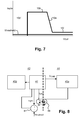
- the plot is similar to that shown in figure 3 ; however in this case, where the output voltage exceeds an upper bound 51, a abnormally high current 10d is driven through the optocoupler's LED 46a. Since this abnormally high current 10d exceeds an overvoltage protection threshold value or upper bound 52, the controller is able to recognize that a malfunction has occurred.
- the abnormally high current 10d increases with yet further increase in output voltage, however, the skilled person will appreciate that the current may be invariant with further increases in output voltage, or even fall with such increases.
- Another way of preventing the anomalous situation would be to provide extra timing information, which checks if the feedback current override takes a longer time than expected or desired, as an indication of a malfunction. If a malfunction is indicated, action can be taken, for instance to disable the converter or disable the Voutprim measurement overriding mechanism.
- FIG. 6 An arrangement for using the over-voltage protection method is shown in block diagram form in figure 6 .
- the figure is substantially the same as that in figure 4 , and like numerals are used to reference like components; however, in this case the secondary side control block 45a includes an over-voltage protection control element 45c
- the potential problem of a low output voltage being insufficient to drive the optocoupler is resolved by use of a minimum current threshold Ithreshold).
- a representation of the output current of the optocoupler is compared with a threshold, in order to define an overriding condition for the optocoupler output.
- the control of the primary side is defined such that the current corresponding to the minimum required output power is larger than the minimum value of the output current of the optocoupler, thereby ensuring that the output can regulate to a minimum output power.
- FIG. 7 A graph of the feedback current against output voltage for this embodiment is shown in figure 7 , and the corresponding block diagram in figure 8 .
- sections 10b and 10a of the feedback current again form a monotonically decreasing function of voltage, with section 10b being a flat and section 10a falling linearly.
- section 10a does not fall to zero with increasing output voltage, but rather is clamped so as not to be able to fall below a minimum value as shown at 10f under normal Vout conditions. This value is greater than that a predetermined current threshold level (Ithreshold).
- Ithreshold a predetermined current threshold level
- the current is made to fall sharply at 10c', to zero - typically by switching off the output current from the error amplifier. Since this is less than the threshold currents, the control is able to determine that the converter is operating in a low voltage regime.
- FIG 8 The corresponding block diagram in use is shown in figure 8 .
- This arrangement is similar to that shown in figures 4 and 6 ; however, in this case the output current lopto from the optocoupler is also used to provide an input into a comparator 81.
- Comparator 81 compares this current (I Opto) with the threshold currents (I threshold), and if it is determined that the Opto current is below the threshold, the converter is determined to be in a low voltage mode.
- a "monotonically decreasing" function is a function which does not increase; that is to say the function can either decrease or remain flat (i.e. neither increase nor decrease), or a combination of decrease and remain flat.
- a controller for a Switched Mode Power Supply having opto-coupler-based feedback from secondary to primary side has been disclosed, in which the optocoupler current varies inversely with the output voltage over a voltage control range.
- the converter is thereby enabled to consume less power than do conventional converters, when in lower-power standby mode.
- Also disclosed have been low-voltage startup and over-voltage protection arrangements combined with such a controller.
- Corresponding methods have been also disclosed.
Landscapes
- Engineering & Computer Science (AREA)
- Power Engineering (AREA)
- Dc-Dc Converters (AREA)
Abstract
Description
- This invention relates to switched mode power supplies (SMPSs), to controllers therefore and to methods of controlling SMPSs.
- Switched mode power converters, in particular but not limited to AC-DC converters, typically employ feedback from the secondary to the primary side in order to control the power of the converter. For many applications, however, electrical isolation is required between the two sides, typically in order to protect the user on the secondary side from relatively high voltages on the primary side (such as mains voltages). For such applications, an optocoupler is a preferred means to provide the feedback across the isolation, since feedback information is transferred from the electrical domain to an optical domain and back.
- In known feedback systems, the optocoupler is used to transfer an error signal (Vout - Voutref), indicative of the difference between the actual output voltage (Vout) and the desired output voltage (Voutref). The feedback current on the output side of the optocoupler (that is to say on the primary side of the converter), increases typically linearly with the error signal, has shown schematically in
figure 1 , which shows a plot of the output current (Iopto) 10 from the optocoupler, against the converter output voltage (Voutout). The feedback current lopto is typically directly related to the input current (Ioptin) driving the optocoupler (that is to say, on the secondary side of the optocoupler) - for instance, the feedback current lopto may be directly proportional to the input current (Ioptin), through a gain factor g. In some implementations, for converter voltages below or equal to Voutref, the feedback current is zero, whilst above Voutref the current increases linearly with the error signal (Vout-Voutref). Further, the error loop may include frequency-dependant elements for implementing integrating and/or differentiating actions. - Under low-power, or no load, conditions the current required by the optocoupler to feedback the error signal can be relatively high. In particular to increase converter efficiencies at low load, there is an ongoing desire to reduce the power consumption in the feedback mechanism.
- According to a first aspect of the present invention, there is provided a controller configured to control a switched mode power converter, the switched mode power converter having a primary side, a secondary side isolated therefrom and for providing an output voltage, and an optocoupler therebetween for providing feedback information to the primary side from the secondary side and drawing, in use, a feedback current from the secondary side, wherein the feedback information is dependant on the output voltage and the controller is configured to provide that the feedback current monotonically decreases with increasing output voltage between a threshold voltage and at least an upper bound. Of course, it will be appreciated that a monotonically decreasing function may be flat, or invariant, over part of its domain. Thus the optocoupler may consume less power, in a standby mode, than in conventional arrangements.
- In embodiments the controller is configured such that the feedback current is invariant with the output voltage between the threshold voltage and a reference voltage (Voutref), which reference voltage is higher than the threshold voltage. In these embodiments, the feedback current falls only over an upper part of the range of output-voltage between the threshold voltage and the upper bound. In other embodiments, the feedback current falls over the lower part of the range, but across this lower part of the range, the feedback current is still sufficiently high to request maximum output power. In some embodiments the controller is configured such that the feedback current either is inversely proportional to the output voltage above the reference voltage (Voutref) or decreases linearly with increasing output voltage above the reference voltage (Voutref).
- In embodiments, the controller is configured to receive a signal (Voutprim) from the primary side indicative the output voltage (Vout), and wherein the controller is further configured to override the feedback information from the optocoupler with the signal (Voutprim) when the output voltage is less than the threshold voltage.
- In embodiments the controller is configured to provide an over-voltage feedback current in the case that the output voltage is above the upper bound.
- In some embodiments the controller further comprises a timer for triggering the over-voltage feedback current only after a predetermined time has elapsed.
- In embodiments the controller is configured to provide a minimum feedback current, in the case that the output voltage is above the upper bound. In embodiments the controller is configured to override the feedback information from the optocoupler in the case that the feedback information is less than a predetermined threshold current which is less than the minimum feedback current.
- According to another aspect of the present invention, there is provided a switched mode power converter comprising a controller mentioned above.
- According to another aspect of the present invention, there is provided a method of controlling a switched mode power converter having a primary side, a secondary side isolated therefrom and for providing an output voltage, and an optocoupler therebetween for providing feedback information and drawing, in use, a feedback current from the secondary side, the method comprising providing feedback information to the primary side from the secondary side dependant on the output voltage and generating the feedback current such that it monotonically decreases with increasing output voltage between a threshold voltage and at least an upper bound.
- In embodiments the feedback current is invariant with the output voltage between the threshold voltage and a reference voltage (Voutref). Thus, the feedback current may have, in part, a flat profile, which does not change as the output voltage changes.
- In embodiments the feedback current either varies in inverse proportion to the output voltage above the reference voltage (Voutref) or decreases linearly with increasing output voltage above the reference voltage (Voutref).
- In embodiments of the invention, the method further comprises measuring a signal (Voutprim) on the primary side indicative the output voltage (Vout), and overriding the feedback information from the optocoupler with the signal in the case that the output voltage is less than the threshold voltage. In embodiments the controller provides an over-voltage feedback current in the case that the output voltage is above the upper bound. In embodiments the over-voltage feedback current is triggered only once the output voltage has been above the upper bound for a predetermined period.
- In embodiments the feedback current is set to a minimum value (10f), in the case that the output voltage is above the upper bound. In embodiments the controller overrides the feedback information from the optocoupler, in the case that the feedback information is less than a predetermined threshold value which is less than the minimum current value (10f).
- According to a further aspect of the present invention, there is provided a computer program, which when run on a computer, causes the computer to configure a controller as described above, or to operate a method as described above.
- These and other aspects of the invention will be apparent from, and elucidated with reference to, the embodiments described hereinafter.
- Embodiments of the invention will be described, by way of example only, with reference to the drawings, in which:
-
figure 1 shows a graph of optocoupler current against output voltage according to known converters; -
figure 2 shows a graph of optocoupler current against output voltage according to embodiments of the invention; -
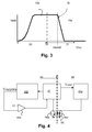
figure 3 shows a graph of optocoupler current against output voltage, including under-voltage override according to an embodiment of the invention; -
figure 4 shows a block diagram of a controller according to an embodiment of the invention; -
figure 5 shows a graph of optocoupler current against output voltage, including under-voltage override and overvoltage protection, according to another embodiment of the invention; -
Figure 6 shows a block diagram of a controller operable according to the graph offigure 5 ; -
figure 7 shows a graph of optocoupler current against output voltage according to a further embodiments of the invention; and -
figure 8 shows a block diagram of a controller operable according to the graph offigure 7 . - It should be noted that the figure are diagrammatic and not drawn to scale. Relative dimensions and proportions of parts of these figure have been shown exaggerated or reduced in size, for the sake of clarity and convenience in the drawings. The same reference signs are generally used to refer to corresponding or similar feature in modified and different embodiments
- As shown in
figure 1 , conventional arrangements of the feedback circuitry provides that a higher value of the output voltage results in a higher value of the optocoupler output current (hereinafter also referred to as the feedback current); the high opto-current is evaluated by the controller to be a request for lower power, and the converter is controlled in order to reduce the output power. Conversely, a low feedback current is evaluated by the controller to be a request for higher power, so the converter is adjusted in order to increase the output power. One important reason to choose this arrangement is to ensure reliable start up: at a low output voltage, the secondary circuit is not supplied with a sufficiently high supply voltage to drive the optocoupler, resulting in zero feedback current. As zero feedback current is a low current, this is interpreted by the controller as a request for higher power, so the power is increased - resulting in reliable start-up. - However, this can result in undesirable power consumption during standby mode, when the load is extremely low. Standby mode can exist for significant periods for systems such as power adaptors. In standby mode, the output voltage remains high, even though only low power is drawn. Due to the output voltage being maintained during this operation, the opto-coupler continues to draw high input current, which can result in a power consumption on the secondary side typically of the order 50 to 100 mW. Moreover, since this power has to be supplied by the primary side, there is a further power loss due to the less-than-unity conversion efficiency of any converter; thus, the situation is even worse, and the optocoupler's drain on the input power can be typically 60 to 200 mW.
- In order to reduce the loss due to the optocoupler under no load, or standby, conditions, it is thus desirable to "invert" the operation of the optocoupler, as shown figuratively in
figure 2 ; then, for increasing output voltage (Vout) above the reference voltage (Voutref), the current drawn by the optocoupler decreases.Figure 2 shows the optocoupler current 10 against output voltage according to embodiments of the invention. For voltages greater than the reference voltage Voutref the current 10a decreases with increasing voltage. In the embodiment shown, the decrease is linear with the error (Vout - Voutref); however, other relationships such as quadratic or reciprocal could also be used. In general terms, provided the derivative d(lopto)/d(Vout) is negative, any relationship could be used. Moreover, frequency-dependant components, such as capacitors, may be used in the feed-back loop, and the decreasing function may then be made to depend either in addition, or alternatively, on either a time-integral and/or a differential of (Vout-Voutref). - For voltages less than the reference voltage, the current 10b is flat, or invariant with voltage, at a nominal first maximum level. In practice, the current need not be flat for voltages lower than the reference voltage; it is sufficient merely that the current is sufficiently high to require that the SMPS provides the maximum desired output current at the regulated output voltage.
- Thus according to this arrangement, the gain of the feedback comprising optocoupler is negative, rather than positive according to conventional arrangements. From one viewpoint, then, it may be considered that the feedback, or more accurately of the gain of the feedback, has inverted polarity.
- With this arrangement, a demand from the secondary side for more power, that is to say a low value of Vout, results in an increased feedback current. In standby mode, the output voltage Vout is high, which results in a low optocoupler current: this significantly reduces the power consumption in standby mode.
- However, this approach gives rise to a significant problem during start-up and in overcurrent situations. An overcurrent situation is one in which the current drawn from the converter is larger than the maximum current that can be consistently delivered. Then the part of the desired current that cannot be delivered will discharge the output capacitor of the supply, resulting in a decrease in output voltage - which is equivalent to the output voltage at startup being low. In start-up and overcurrent situations, as shown at the left-hand side of
figure 2 , if the output voltage (Vout) is too low to support operation of the optocoupler, both the optocoupler input current and the optocoupler output (feedback) current below the nominal first maximum level. However, the controller would interpret this, that is to say, a low feedback current, as an indication that the voltage is too high, and thus that less power is required. As a consequence, the output voltage will not be able to rise, and start-up will not properly occur. - One solution to this problem is to combine the inverted polarity gain as described above with reference to
figure 2 , with a supplementary measurement of the output voltage made on the primary side (Voutprim). When Voutprim indicates that the upper voltage is below a certain threshold level (V1), the inverted polarity gain is overridden. This is illustrated infigure 3 . The figure shows, asfigure 2 , the feedback current 10 plotted against output voltage. Above a reference voltage (Voutref) the feedback current falls with increasing voltage. However, the controller is only reliant on the feedback current forvoltages 31 above a threshold voltage (V1). Forvoltages 30 below the threshold, the feedback loop is overridden. The threshold voltage is set sufficiently high that the optocoupler is able to operate properly at this voltage. Below the threshold value, the converter operation is fully determined by the primary side control, and can for example be set according to a fixed value of a control parameter such as primary peak current, duty cycle, on-time or frequency, as will be known to those skilled in the art. In other embodiments, the setting for the control parameter is combined with a time-varying element, for example, a slow increase over a certain time interval, in order to provide a soft start, or a value which depends on the rate of rise of Voutprim, that is to say depends on dV/dT, to result in a well-defined output voltage rise during start-up. - An SMPS arrangement for using this method is shown in block diagram form in
figure 4. Figure 4 shows apower converter 41, which operates across the mains isolation 42 between aprimary side 43 and a second recite 44. On the secondary side there is a secondaryside control block 45a, which receives as input the output voltage (Vout). The secondaryside control block 45a drives theLED 46a of anoptocoupler 46. The photo diode 46p ofoptocoupler 46 feeds this information back to thepower converter 41. On the primary side there is the primaryside control block 45b, which provides a measurement (Voutprim) indicative of the output voltage, by means which will be immediately apparent to those skilled in the art; for example by means of a primary side auxiliary transform or winding. The measurement (Voutprim) indicative of the output voltage is compared with a the threshold voltage V1 in acomparator 45d, and the result is supplied to the converter to determine whether control of the converter is by means of the feedback current, or the measurement (Voutprim) indicative of the output voltage. - Use of the arrangement shown in
figure 4 could result in an anomalous, or potentially unsafe, situation where the input measurement circuit to determine Voutprim malfunctions - for example, due to a broken or shorted connection in the auxiliary winding circuit. The optocoupler may then be permanently overridden, resulting in an uncontrolled output voltage. - To prevent this, in one embodiment, is there is provided an over-voltage protection at the secondary side, which supplies additional information to the primary side. This additional information may be sent via the optocoupler by applying a current level outside the normal operation range. Thus, if the output voltage exceeds an upper bound, both the inverted polarity feedback and the Voutprim measurement are overridden by the abnormally high current on the optocoupler. Corrective actions, which may be applied when overvoltage is determined, may include a cycle-by-cycle action, wherein the converter is disabled when the level is above the over-voltage threshold but reenabled when the level falls below this threshold; alternatively a latch may be applied such that the converter is disabled when the level is above the threshold and a safe restart is forced.
-
Figure 5 shows a graph of the feedback current against output voltage according to this embodiment. The plot is similar to that shown infigure 3 ; however in this case, where the output voltage exceeds an upper bound 51, a abnormally high current 10d is driven through the optocoupler'sLED 46a. Since this abnormally high current 10d exceeds an overvoltage protection threshold value or upper bound 52, the controller is able to recognize that a malfunction has occurred. As shown, the abnormally high current 10d increases with yet further increase in output voltage, however, the skilled person will appreciate that the current may be invariant with further increases in output voltage, or even fall with such increases. Furthermore, as shown in the figure, there may be includedhysteresis 10e around the upper bound 51, in order to prevent bouncing between the normal-voltage, and overvoltage protected, states. - Another way of preventing the anomalous situation would be to provide extra timing information, which checks if the feedback current override takes a longer time than expected or desired, as an indication of a malfunction. If a malfunction is indicated, action can be taken, for instance to disable the converter or disable the Voutprim measurement overriding mechanism.
- An arrangement for using the over-voltage protection method is shown in block diagram form in
figure 6 . The figure is substantially the same as that infigure 4 , and like numerals are used to reference like components; however, in this case the secondaryside control block 45a includes an over-voltageprotection control element 45c - In another embodiment, the potential problem of a low output voltage being insufficient to drive the optocoupler is resolved by use of a minimum current threshold Ithreshold). In this embodiment, a representation of the output current of the optocoupler is compared with a threshold, in order to define an overriding condition for the optocoupler output. The control of the primary side is defined such that the current corresponding to the minimum required output power is larger than the minimum value of the output current of the optocoupler, thereby ensuring that the output can regulate to a minimum output power. As the overriding condition for the optocoupler output is now based on the optocoupler current, additional (primary side) sensing of output voltage is not necessary: absent any Voutprim measuring circuitry the above anomalous situation where such circuitry malfunctions is precluded.
- A graph of the feedback current against output voltage for this embodiment is shown in
figure 7 , and the corresponding block diagram infigure 8 . Infigure 7 , similar to the previous embodiments,sections section 10b being a flat andsection 10a falling linearly. However, in this embodiment,section 10a does not fall to zero with increasing output voltage, but rather is clamped so as not to be able to fall below a minimum value as shown at 10f under normal Vout conditions. This value is greater than that a predetermined current threshold level (Ithreshold). At low voltages, the current is made to fall sharply at 10c', to zero - typically by switching off the output current from the error amplifier. Since this is less than the threshold currents, the control is able to determine that the converter is operating in a low voltage regime. - The corresponding block diagram in use is shown in
figure 8 . This arrangement is similar to that shown infigures 4 and6 ; however, in this case the output current lopto from the optocoupler is also used to provide an input into acomparator 81.Comparator 81 compares this current (I Opto) with the threshold currents (I threshold), and if it is determined that the Opto current is below the threshold, the converter is determined to be in a low voltage mode. - For the sake of completeness and the avoidance of doubt, it is hereby confirmed that a "monotonically decreasing" function is a function which does not increase; that is to say the function can either decrease or remain flat (i.e. neither increase nor decrease), or a combination of decrease and remain flat.
- In summary, from one viewpoint, a controller for a Switched Mode Power Supply having opto-coupler-based feedback from secondary to primary side, has been disclosed, in which the optocoupler current varies inversely with the output voltage over a voltage control range. The converter is thereby enabled to consume less power than do conventional converters, when in lower-power standby mode. Also disclosed have been low-voltage startup and over-voltage protection arrangements combined with such a controller. Corresponding methods have been also disclosed.
- From reading the present disclosure, other variations and modifications will be apparent to the skilled person. Such variations and modifications may involve equivalent and other features which are already known in the art of power converters, and which may be used instead of, or in addition to, features already described herein.
- Although the appended claims are directed to particular combinations of features, it should be understood that the scope of the disclosure of the present invention also includes any novel feature or any novel combination of features disclosed herein either explicitly or implicitly or any generalisation thereof, whether or not it relates to the same invention as presently claimed in any claim and whether or not it mitigates any or all of the same technical problems as does the present invention.
- Features which are described in the context of separate embodiments may also be provided in combination in a single embodiment. Conversely, various features which are, for brevity, described in the context of a single embodiment, may also be provided separately or in any suitable sub-combination.
- The applicant hereby gives notice that new claims may be formulated to such features and/or combinations of such features during the prosecution of the present application or of any further application derived therefrom.
- For the sake of completeness it is also stated that the term "comprising" does not exclude other elements or steps, the term "a" or "an" does not exclude a plurality, a single processor or other unit may fulfil the functions of several means recited in the claims and reference signs in the claims shall not be construed as limiting the scope of the claims.
Claims (18)
- A controller (45a, 45b, 45d) configured to control a switched mode power converter, the switched mode power converter having a primary side (43), a secondary side (44) isolated therefrom and for providing an output voltage, and an optocoupler (46) therebetween for providing feedback information to the primary side from the secondary side and drawing, in use, a feedback current from the secondary side,
wherein the feedback information is dependant on the output voltage (Vout) and
the controller is configured to provide that the feedback current (Iopto) monotonically decreases with increasing output voltage between a threshold voltage (V1) and at least an upper bound. - A controller according to claim 1, wherein the controller is configured such that the feedback current is invariant with the output voltage between the threshold voltage and a reference voltage (Voutref), which reference voltage is higher than the threshold voltage.
- A controller according to claim 2, wherein the controller is configured such that the feedback current either is inversely proportional to the output voltage above the reference voltage (Voutref) or decreases linearly with increasing output voltage above the reference voltage (Voutref).
- A controller according to any preceding claim, configured to receive a signal (Voutprim) from the primary side indicative the output voltage (Vout), and wherein the controller is further configured to override the feedback information from the optocoupler with the signal (Voutprim) when the output voltage is less than the threshold voltage.
- A controller according to claim 4, wherein the controller is configured to provide an over-voltage feedback current (10d) in the case that the output voltage is above the upper bound.
- A controller according to claim 5, further comprising a timer for triggering the over-voltage feedback current only after a predetermined time has elapsed.
- A controller according to any of claims 1 to 3, wherein the controller is configured to provide a minimum feedback current, in the case that the output voltage is above the upper bound.
- A controller according to claim 7, wherein the controller is configured to override the feedback information from the optocoupler in the case that the feedback information is less than a predetermined threshold current.
- A switched mode power converter comprising a controller as claimed in any preceding claim.
- A method of controlling a switched mode power converter having a primary side, a secondary side isolated therefrom and for providing an output voltage, and an optocoupler therebetween for providing feedback information and drawing, in use, a feedback current from the secondary side,
the method comprising providing feedback information to the primary side from the secondary side dependant on the output voltage and generating the feedback current such that it monotonically decreases with increasing output voltage between a threshold voltage and at least an upper bound. - The method of claim 10, wherein the feedback current is invariant with the output voltage between the threshold voltage and a reference voltage (Voutref).
- The method of claim 11 wherein the feedback current either varies in inverse proportion to the output voltage above the reference voltage (Voutref) or decreases linearly with increasing output voltage above the reference voltage (Voutref).
- The method of any of claims 10 to 12, further comprising measuring a signal (Voutprim) on the primary side indicative the output voltage (Vout), and overriding the feedback information from the optocoupler with the signal in the case that the output voltage is less than the threshold voltage.
- The method of claim 13 wherein the controller provides an over-voltage feedback current in the case that the output voltage is above the upper bound.
- The method of claim 14, wherein the over-voltage feedback current is triggered only once the output voltage has been above the upper bound for a predetermined period.
- The method of any of claims 10 to 12, wherein the feedback current is set to a minimum value (10f), in the case that the output voltage is above the upper bound.
- The method of claim 16, wherein the controller overrides the feedback information from the optocoupler, in the case that the feedback information is less than a predetermined threshold value which is less than the minimum current value (10f).
- A computer program, which when run on a computer, causes the computer to configure the controller of any one claims 1 to 8, or to operate the method of any of claims 10 to 16.
Priority Applications (3)
| Application Number | Priority Date | Filing Date | Title |
|---|---|---|---|
| EP09176055A EP2323247B1 (en) | 2009-11-16 | 2009-11-16 | A controller for a switched mode power supply (smps), a smps, and a method of controlling a smps |
| CN2010105488738A CN102064679A (en) | 2009-11-16 | 2010-11-12 | A controller for a switched mode power supply (SMPS), a SMPS, and a method of controlling a SMPS |
| US12/946,761 US8441816B2 (en) | 2009-10-16 | 2010-11-15 | Controller for a switched mode power supply (SMPS), a SMPS, and a method of controlling a SMPS |
Applications Claiming Priority (1)
| Application Number | Priority Date | Filing Date | Title |
|---|---|---|---|
| EP09176055A EP2323247B1 (en) | 2009-11-16 | 2009-11-16 | A controller for a switched mode power supply (smps), a smps, and a method of controlling a smps |
Publications (2)
| Publication Number | Publication Date |
|---|---|
| EP2323247A1 true EP2323247A1 (en) | 2011-05-18 |
| EP2323247B1 EP2323247B1 (en) | 2013-01-09 |
Family
ID=42079091
Family Applications (1)
| Application Number | Title | Priority Date | Filing Date |
|---|---|---|---|
| EP09176055A Not-in-force EP2323247B1 (en) | 2009-10-16 | 2009-11-16 | A controller for a switched mode power supply (smps), a smps, and a method of controlling a smps |
Country Status (3)
| Country | Link |
|---|---|
| US (1) | US8441816B2 (en) |
| EP (1) | EP2323247B1 (en) |
| CN (1) | CN102064679A (en) |
Cited By (1)
| Publication number | Priority date | Publication date | Assignee | Title |
|---|---|---|---|---|
| WO2023285208A1 (en) * | 2021-07-13 | 2023-01-19 | Signify Holding B.V. | Overvoltage protection integrated in the module temperature protection |
Families Citing this family (5)
| Publication number | Priority date | Publication date | Assignee | Title |
|---|---|---|---|---|
| EP2515453B1 (en) * | 2011-04-19 | 2015-08-05 | ABB Research Ltd. | Communication system for power electronic converters |
| TWI496396B (en) * | 2012-02-18 | 2015-08-11 | Richtek Technology Corp | Isolated power converter circuit and control circuit and control method thereof |
| EP2683068B1 (en) | 2012-07-06 | 2014-09-10 | Nxp B.V. | Control circuit for a switched-mode power supply |
| JP6101493B2 (en) * | 2013-01-15 | 2017-03-22 | ローム株式会社 | Power supply device, AC adapter, electronic device, and power supply system |
| WO2022269411A1 (en) | 2021-06-21 | 2022-12-29 | Silanna Asia Pte Ltd | Feedback voltage modulation to reduce power converter quiescent current |
Citations (2)
| Publication number | Priority date | Publication date | Assignee | Title |
|---|---|---|---|---|
| WO2004030194A1 (en) * | 2002-09-30 | 2004-04-08 | Infineon Technologies Ag | Switching mode power supplies |
| EP1648080A1 (en) | 2004-10-13 | 2006-04-19 | Infineon Technologies AG | Drive circuit for a switch in a switching converter |
Family Cites Families (5)
| Publication number | Priority date | Publication date | Assignee | Title |
|---|---|---|---|---|
| KR100418623B1 (en) * | 1998-12-18 | 2004-06-18 | 페어차일드코리아반도체 주식회사 | Switching mode power supply with constant power control circuit |
| US7057907B2 (en) * | 2003-11-21 | 2006-06-06 | Fairchild Semiconductor Corporation | Power converter having improved control |
| CN1937383A (en) * | 2005-09-22 | 2007-03-28 | 松下电器产业株式会社 | Switch power supply, semiconductor appatatus and controlling method |
| US7881077B2 (en) * | 2007-07-20 | 2011-02-01 | Niko Semiconductor Co., Ltd. | PWM controller with output current limitation |
| JP4543265B2 (en) * | 2007-11-20 | 2010-09-15 | 船井電機株式会社 | Switching power supply |
-
2009
- 2009-11-16 EP EP09176055A patent/EP2323247B1/en not_active Not-in-force
-
2010
- 2010-11-12 CN CN2010105488738A patent/CN102064679A/en active Pending
- 2010-11-15 US US12/946,761 patent/US8441816B2/en not_active Expired - Fee Related
Patent Citations (2)
| Publication number | Priority date | Publication date | Assignee | Title |
|---|---|---|---|---|
| WO2004030194A1 (en) * | 2002-09-30 | 2004-04-08 | Infineon Technologies Ag | Switching mode power supplies |
| EP1648080A1 (en) | 2004-10-13 | 2006-04-19 | Infineon Technologies AG | Drive circuit for a switch in a switching converter |
Cited By (2)
| Publication number | Priority date | Publication date | Assignee | Title |
|---|---|---|---|---|
| WO2023285208A1 (en) * | 2021-07-13 | 2023-01-19 | Signify Holding B.V. | Overvoltage protection integrated in the module temperature protection |
| US12439492B2 (en) | 2021-07-13 | 2025-10-07 | Signify Holding B.V. | Overvoltage protection integrated in the module temperature protection |
Also Published As
| Publication number | Publication date |
|---|---|
| US20110280051A1 (en) | 2011-11-17 |
| EP2323247B1 (en) | 2013-01-09 |
| US8441816B2 (en) | 2013-05-14 |
| CN102064679A (en) | 2011-05-18 |
Similar Documents
| Publication | Publication Date | Title |
|---|---|---|
| US10277130B2 (en) | Primary-side start-up method and circuit arrangement for a series-parallel resonant power converter | |
| US9337739B2 (en) | Power controller with over power protection | |
| US8988902B2 (en) | Power converter controller IC having pins with multiple functions | |
| EP3338352B1 (en) | Power converter with sleep/wake mode | |
| EP2573922B1 (en) | Power supply controller with minimum-sum multi-cycle modulation | |
| EP1675252B1 (en) | PWM control apparatus having a standby mode | |
| CN110011539B (en) | Method and apparatus for implementing unregulated dormant mode in a power converter | |
| US7679938B2 (en) | System and method for providing control for switch-mode power supply | |
| US8358517B2 (en) | Switching power conversion circuit and power supply using same | |
| US20130229832A1 (en) | Controlling a flyback converter for use with a computer system | |
| US8441816B2 (en) | Controller for a switched mode power supply (SMPS), a SMPS, and a method of controlling a SMPS | |
| JP2007014196A (en) | Method for detecting failure in switching power supply and detecting apparatus thereof | |
| WO2001063735A1 (en) | Power converter mode transistioning method and apparatus | |
| JP2007020392A (en) | Method and device for conditional response with respect to fault condition in switching power supply | |
| TWI656722B (en) | High voltage charging control method, power controller, and power supply | |
| CN107222095B (en) | Power converter, integrated circuit and method for soft starting isolated power converter | |
| CN103066825A (en) | A kind of power off method and power supply | |
| US7826239B2 (en) | Overload protection delay circuit for switching power supply | |
| EP2343794A2 (en) | A variable current limiter, a power supply and a point of load converter employing the limiter and a method of operating a non-isolated voltage converter | |
| US10615681B2 (en) | Switching power supply circuit | |
| CN111555621B (en) | Flyback Converter with No-Load Power Control for Reduced Power Dissipation | |
| CN113726175A (en) | Conversion device, controller and power supply control method thereof | |
| EP4340195B1 (en) | POWER REFERENCER CONTROL DEVICE, POWER REFERENCER AND METHOD FOR OPERATION OF A POWER REFERENCER | |
| JP2024175914A (en) | Switching Power Supply Unit | |
| CN118646271A (en) | A method for controlling output voltage of a PSR control chip |
Legal Events
| Date | Code | Title | Description |
|---|---|---|---|
| PUAI | Public reference made under article 153(3) epc to a published international application that has entered the european phase |
Free format text: ORIGINAL CODE: 0009012 |
|
| AK | Designated contracting states |
Kind code of ref document: A1 Designated state(s): AT BE BG CH CY CZ DE DK EE ES FI FR GB GR HR HU IE IS IT LI LT LU LV MC MK MT NL NO PL PT RO SE SI SK SM TR |
|
| AX | Request for extension of the european patent |
Extension state: AL BA RS |
|
| 17P | Request for examination filed |
Effective date: 20111118 |
|
| GRAP | Despatch of communication of intention to grant a patent |
Free format text: ORIGINAL CODE: EPIDOSNIGR1 |
|
| RIN1 | Information on inventor provided before grant (corrected) |
Inventor name: HALBERSTADT, HANS |
|
| GRAS | Grant fee paid |
Free format text: ORIGINAL CODE: EPIDOSNIGR3 |
|
| GRAA | (expected) grant |
Free format text: ORIGINAL CODE: 0009210 |
|
| AK | Designated contracting states |
Kind code of ref document: B1 Designated state(s): AT BE BG CH CY CZ DE DK EE ES FI FR GB GR HR HU IE IS IT LI LT LU LV MC MK MT NL NO PL PT RO SE SI SK SM TR |
|
| REG | Reference to a national code |
Ref country code: GB Ref legal event code: FG4D |
|
| REG | Reference to a national code |
Ref country code: AT Ref legal event code: REF Ref document number: 593234 Country of ref document: AT Kind code of ref document: T Effective date: 20130115 Ref country code: CH Ref legal event code: EP |
|
| REG | Reference to a national code |
Ref country code: IE Ref legal event code: FG4D |
|
| REG | Reference to a national code |
Ref country code: DE Ref legal event code: R096 Ref document number: 602009012626 Country of ref document: DE Effective date: 20130307 |
|
| PG25 | Lapsed in a contracting state [announced via postgrant information from national office to epo] |
Ref country code: SI Free format text: LAPSE BECAUSE OF FAILURE TO SUBMIT A TRANSLATION OF THE DESCRIPTION OR TO PAY THE FEE WITHIN THE PRESCRIBED TIME-LIMIT Effective date: 20130109 |
|
| REG | Reference to a national code |
Ref country code: NL Ref legal event code: VDEP Effective date: 20130109 |
|
| REG | Reference to a national code |
Ref country code: AT Ref legal event code: MK05 Ref document number: 593234 Country of ref document: AT Kind code of ref document: T Effective date: 20130109 |
|
| REG | Reference to a national code |
Ref country code: LT Ref legal event code: MG4D |
|
| PG25 | Lapsed in a contracting state [announced via postgrant information from national office to epo] |
Ref country code: BE Free format text: LAPSE BECAUSE OF FAILURE TO SUBMIT A TRANSLATION OF THE DESCRIPTION OR TO PAY THE FEE WITHIN THE PRESCRIBED TIME-LIMIT Effective date: 20130109 Ref country code: AT Free format text: LAPSE BECAUSE OF FAILURE TO SUBMIT A TRANSLATION OF THE DESCRIPTION OR TO PAY THE FEE WITHIN THE PRESCRIBED TIME-LIMIT Effective date: 20130109 Ref country code: BG Free format text: LAPSE BECAUSE OF FAILURE TO SUBMIT A TRANSLATION OF THE DESCRIPTION OR TO PAY THE FEE WITHIN THE PRESCRIBED TIME-LIMIT Effective date: 20130409 Ref country code: LT Free format text: LAPSE BECAUSE OF FAILURE TO SUBMIT A TRANSLATION OF THE DESCRIPTION OR TO PAY THE FEE WITHIN THE PRESCRIBED TIME-LIMIT Effective date: 20130109 Ref country code: NO Free format text: LAPSE BECAUSE OF FAILURE TO SUBMIT A TRANSLATION OF THE DESCRIPTION OR TO PAY THE FEE WITHIN THE PRESCRIBED TIME-LIMIT Effective date: 20130409 Ref country code: IS Free format text: LAPSE BECAUSE OF FAILURE TO SUBMIT A TRANSLATION OF THE DESCRIPTION OR TO PAY THE FEE WITHIN THE PRESCRIBED TIME-LIMIT Effective date: 20130509 Ref country code: SE Free format text: LAPSE BECAUSE OF FAILURE TO SUBMIT A TRANSLATION OF THE DESCRIPTION OR TO PAY THE FEE WITHIN THE PRESCRIBED TIME-LIMIT Effective date: 20130109 Ref country code: ES Free format text: LAPSE BECAUSE OF FAILURE TO SUBMIT A TRANSLATION OF THE DESCRIPTION OR TO PAY THE FEE WITHIN THE PRESCRIBED TIME-LIMIT Effective date: 20130420 |
|
| PG25 | Lapsed in a contracting state [announced via postgrant information from national office to epo] |
Ref country code: LV Free format text: LAPSE BECAUSE OF FAILURE TO SUBMIT A TRANSLATION OF THE DESCRIPTION OR TO PAY THE FEE WITHIN THE PRESCRIBED TIME-LIMIT Effective date: 20130109 Ref country code: GR Free format text: LAPSE BECAUSE OF FAILURE TO SUBMIT A TRANSLATION OF THE DESCRIPTION OR TO PAY THE FEE WITHIN THE PRESCRIBED TIME-LIMIT Effective date: 20130410 Ref country code: NL Free format text: LAPSE BECAUSE OF FAILURE TO SUBMIT A TRANSLATION OF THE DESCRIPTION OR TO PAY THE FEE WITHIN THE PRESCRIBED TIME-LIMIT Effective date: 20130109 Ref country code: PL Free format text: LAPSE BECAUSE OF FAILURE TO SUBMIT A TRANSLATION OF THE DESCRIPTION OR TO PAY THE FEE WITHIN THE PRESCRIBED TIME-LIMIT Effective date: 20130109 Ref country code: FI Free format text: LAPSE BECAUSE OF FAILURE TO SUBMIT A TRANSLATION OF THE DESCRIPTION OR TO PAY THE FEE WITHIN THE PRESCRIBED TIME-LIMIT Effective date: 20130109 Ref country code: PT Free format text: LAPSE BECAUSE OF FAILURE TO SUBMIT A TRANSLATION OF THE DESCRIPTION OR TO PAY THE FEE WITHIN THE PRESCRIBED TIME-LIMIT Effective date: 20130509 |
|
| PG25 | Lapsed in a contracting state [announced via postgrant information from national office to epo] |
Ref country code: HR Free format text: LAPSE BECAUSE OF FAILURE TO SUBMIT A TRANSLATION OF THE DESCRIPTION OR TO PAY THE FEE WITHIN THE PRESCRIBED TIME-LIMIT Effective date: 20130109 |
|
| PG25 | Lapsed in a contracting state [announced via postgrant information from national office to epo] |
Ref country code: RO Free format text: LAPSE BECAUSE OF FAILURE TO SUBMIT A TRANSLATION OF THE DESCRIPTION OR TO PAY THE FEE WITHIN THE PRESCRIBED TIME-LIMIT Effective date: 20130109 Ref country code: SK Free format text: LAPSE BECAUSE OF FAILURE TO SUBMIT A TRANSLATION OF THE DESCRIPTION OR TO PAY THE FEE WITHIN THE PRESCRIBED TIME-LIMIT Effective date: 20130109 Ref country code: EE Free format text: LAPSE BECAUSE OF FAILURE TO SUBMIT A TRANSLATION OF THE DESCRIPTION OR TO PAY THE FEE WITHIN THE PRESCRIBED TIME-LIMIT Effective date: 20130109 Ref country code: DK Free format text: LAPSE BECAUSE OF FAILURE TO SUBMIT A TRANSLATION OF THE DESCRIPTION OR TO PAY THE FEE WITHIN THE PRESCRIBED TIME-LIMIT Effective date: 20130109 Ref country code: CZ Free format text: LAPSE BECAUSE OF FAILURE TO SUBMIT A TRANSLATION OF THE DESCRIPTION OR TO PAY THE FEE WITHIN THE PRESCRIBED TIME-LIMIT Effective date: 20130109 |
|
| PLBE | No opposition filed within time limit |
Free format text: ORIGINAL CODE: 0009261 |
|
| STAA | Information on the status of an ep patent application or granted ep patent |
Free format text: STATUS: NO OPPOSITION FILED WITHIN TIME LIMIT |
|
| PG25 | Lapsed in a contracting state [announced via postgrant information from national office to epo] |
Ref country code: CY Free format text: LAPSE BECAUSE OF FAILURE TO SUBMIT A TRANSLATION OF THE DESCRIPTION OR TO PAY THE FEE WITHIN THE PRESCRIBED TIME-LIMIT Effective date: 20130109 |
|
| 26N | No opposition filed |
Effective date: 20131010 |
|
| PG25 | Lapsed in a contracting state [announced via postgrant information from national office to epo] |
Ref country code: IT Free format text: LAPSE BECAUSE OF FAILURE TO SUBMIT A TRANSLATION OF THE DESCRIPTION OR TO PAY THE FEE WITHIN THE PRESCRIBED TIME-LIMIT Effective date: 20130109 |
|
| REG | Reference to a national code |
Ref country code: DE Ref legal event code: R097 Ref document number: 602009012626 Country of ref document: DE Effective date: 20131010 |
|
| REG | Reference to a national code |
Ref country code: CH Ref legal event code: PL |
|
| PG25 | Lapsed in a contracting state [announced via postgrant information from national office to epo] |
Ref country code: MC Free format text: LAPSE BECAUSE OF FAILURE TO SUBMIT A TRANSLATION OF THE DESCRIPTION OR TO PAY THE FEE WITHIN THE PRESCRIBED TIME-LIMIT Effective date: 20130109 Ref country code: CH Free format text: LAPSE BECAUSE OF NON-PAYMENT OF DUE FEES Effective date: 20131130 Ref country code: LI Free format text: LAPSE BECAUSE OF NON-PAYMENT OF DUE FEES Effective date: 20131130 |
|
| REG | Reference to a national code |
Ref country code: IE Ref legal event code: MM4A |
|
| PG25 | Lapsed in a contracting state [announced via postgrant information from national office to epo] |
Ref country code: IE Free format text: LAPSE BECAUSE OF NON-PAYMENT OF DUE FEES Effective date: 20131116 |
|
| PG25 | Lapsed in a contracting state [announced via postgrant information from national office to epo] |
Ref country code: SM Free format text: LAPSE BECAUSE OF FAILURE TO SUBMIT A TRANSLATION OF THE DESCRIPTION OR TO PAY THE FEE WITHIN THE PRESCRIBED TIME-LIMIT Effective date: 20130109 |
|
| PG25 | Lapsed in a contracting state [announced via postgrant information from national office to epo] |
Ref country code: TR Free format text: LAPSE BECAUSE OF FAILURE TO SUBMIT A TRANSLATION OF THE DESCRIPTION OR TO PAY THE FEE WITHIN THE PRESCRIBED TIME-LIMIT Effective date: 20130109 |
|
| PG25 | Lapsed in a contracting state [announced via postgrant information from national office to epo] |
Ref country code: MK Free format text: LAPSE BECAUSE OF FAILURE TO SUBMIT A TRANSLATION OF THE DESCRIPTION OR TO PAY THE FEE WITHIN THE PRESCRIBED TIME-LIMIT Effective date: 20130109 Ref country code: HU Free format text: LAPSE BECAUSE OF FAILURE TO SUBMIT A TRANSLATION OF THE DESCRIPTION OR TO PAY THE FEE WITHIN THE PRESCRIBED TIME-LIMIT; INVALID AB INITIO Effective date: 20091116 Ref country code: LU Free format text: LAPSE BECAUSE OF NON-PAYMENT OF DUE FEES Effective date: 20131116 |
|
| PG25 | Lapsed in a contracting state [announced via postgrant information from national office to epo] |
Ref country code: MT Free format text: LAPSE BECAUSE OF FAILURE TO SUBMIT A TRANSLATION OF THE DESCRIPTION OR TO PAY THE FEE WITHIN THE PRESCRIBED TIME-LIMIT Effective date: 20130109 |
|
| REG | Reference to a national code |
Ref country code: FR Ref legal event code: PLFP Year of fee payment: 7 |
|
| REG | Reference to a national code |
Ref country code: FR Ref legal event code: PLFP Year of fee payment: 8 |
|
| REG | Reference to a national code |
Ref country code: FR Ref legal event code: PLFP Year of fee payment: 9 |
|
| REG | Reference to a national code |
Ref country code: FR Ref legal event code: PLFP Year of fee payment: 10 |
|
| P01 | Opt-out of the competence of the unified patent court (upc) registered |
Effective date: 20230724 |
|
| PGFP | Annual fee paid to national office [announced via postgrant information from national office to epo] |
Ref country code: GB Payment date: 20231019 Year of fee payment: 15 |
|
| PGFP | Annual fee paid to national office [announced via postgrant information from national office to epo] |
Ref country code: FR Payment date: 20231019 Year of fee payment: 15 Ref country code: DE Payment date: 20231019 Year of fee payment: 15 |
|
| REG | Reference to a national code |
Ref country code: DE Ref legal event code: R119 Ref document number: 602009012626 Country of ref document: DE |
|
| GBPC | Gb: european patent ceased through non-payment of renewal fee |
Effective date: 20241116 |
|
| PG25 | Lapsed in a contracting state [announced via postgrant information from national office to epo] |
Ref country code: DE Free format text: LAPSE BECAUSE OF NON-PAYMENT OF DUE FEES Effective date: 20250603 |
|
| PG25 | Lapsed in a contracting state [announced via postgrant information from national office to epo] |
Ref country code: GB Free format text: LAPSE BECAUSE OF NON-PAYMENT OF DUE FEES Effective date: 20241116 |
|
| PG25 | Lapsed in a contracting state [announced via postgrant information from national office to epo] |
Ref country code: FR Free format text: LAPSE BECAUSE OF NON-PAYMENT OF DUE FEES Effective date: 20241130 |