EP2321880B1 - Elektrische verbinder und baugruppen mit buchsenkontakt - Google Patents
Elektrische verbinder und baugruppen mit buchsenkontakt Download PDFInfo
- Publication number
- EP2321880B1 EP2321880B1 EP20090788976 EP09788976A EP2321880B1 EP 2321880 B1 EP2321880 B1 EP 2321880B1 EP 20090788976 EP20090788976 EP 20090788976 EP 09788976 A EP09788976 A EP 09788976A EP 2321880 B1 EP2321880 B1 EP 2321880B1
- Authority
- EP
- European Patent Office
- Prior art keywords
- mating
- connector
- socket
- housing
- connector assembly
- Prior art date
- Legal status (The legal status is an assumption and is not a legal conclusion. Google has not performed a legal analysis and makes no representation as to the accuracy of the status listed.)
- Active
Links
- 238000000429 assembly Methods 0.000 title description 8
- 230000000712 assembly Effects 0.000 title description 5
- 230000013011 mating Effects 0.000 claims description 55
- 239000004020 conductor Substances 0.000 claims description 15
- 230000008878 coupling Effects 0.000 claims description 5
- 238000010168 coupling process Methods 0.000 claims description 5
- 238000005859 coupling reaction Methods 0.000 claims description 5
- 230000037431 insertion Effects 0.000 claims 1
- 238000003780 insertion Methods 0.000 claims 1
- 230000035939 shock Effects 0.000 description 6
- 230000000295 complement effect Effects 0.000 description 3
- 230000005540 biological transmission Effects 0.000 description 2
- 238000013500 data storage Methods 0.000 description 2
- 239000003989 dielectric material Substances 0.000 description 2
- 238000000034 method Methods 0.000 description 2
- 238000000465 moulding Methods 0.000 description 2
- RYGMFSIKBFXOCR-UHFFFAOYSA-N Copper Chemical compound [Cu] RYGMFSIKBFXOCR-UHFFFAOYSA-N 0.000 description 1
- 241001417495 Serranidae Species 0.000 description 1
- 229910052802 copper Inorganic materials 0.000 description 1
- 239000010949 copper Substances 0.000 description 1
- 239000000463 material Substances 0.000 description 1
- 230000002688 persistence Effects 0.000 description 1
Images


Classifications
-
- H—ELECTRICITY
- H01—ELECTRIC ELEMENTS
- H01R—ELECTRICALLY-CONDUCTIVE CONNECTIONS; STRUCTURAL ASSOCIATIONS OF A PLURALITY OF MUTUALLY-INSULATED ELECTRICAL CONNECTING ELEMENTS; COUPLING DEVICES; CURRENT COLLECTORS
- H01R13/00—Details of coupling devices of the kinds covered by groups H01R12/70 or H01R24/00 - H01R33/00
- H01R13/02—Contact members
- H01R13/04—Pins or blades for co-operation with sockets
- H01R13/05—Resilient pins or blades
- H01R13/052—Resilient pins or blades co-operating with sockets having a circular transverse section
-
- H—ELECTRICITY
- H01—ELECTRIC ELEMENTS
- H01R—ELECTRICALLY-CONDUCTIVE CONNECTIONS; STRUCTURAL ASSOCIATIONS OF A PLURALITY OF MUTUALLY-INSULATED ELECTRICAL CONNECTING ELEMENTS; COUPLING DEVICES; CURRENT COLLECTORS
- H01R12/00—Structural associations of a plurality of mutually-insulated electrical connecting elements, specially adapted for printed circuits, e.g. printed circuit boards [PCB], flat or ribbon cables, or like generally planar structures, e.g. terminal strips, terminal blocks; Coupling devices specially adapted for printed circuits, flat or ribbon cables, or like generally planar structures; Terminals specially adapted for contact with, or insertion into, printed circuits, flat or ribbon cables, or like generally planar structures
- H01R12/70—Coupling devices
- H01R12/71—Coupling devices for rigid printing circuits or like structures
- H01R12/72—Coupling devices for rigid printing circuits or like structures coupling with the edge of the rigid printed circuits or like structures
- H01R12/722—Coupling devices for rigid printing circuits or like structures coupling with the edge of the rigid printed circuits or like structures coupling devices mounted on the edge of the printed circuits
- H01R12/724—Coupling devices for rigid printing circuits or like structures coupling with the edge of the rigid printed circuits or like structures coupling devices mounted on the edge of the printed circuits containing contact members forming a right angle
-
- H—ELECTRICITY
- H01—ELECTRIC ELEMENTS
- H01R—ELECTRICALLY-CONDUCTIVE CONNECTIONS; STRUCTURAL ASSOCIATIONS OF A PLURALITY OF MUTUALLY-INSULATED ELECTRICAL CONNECTING ELEMENTS; COUPLING DEVICES; CURRENT COLLECTORS
- H01R13/00—Details of coupling devices of the kinds covered by groups H01R12/70 or H01R24/00 - H01R33/00
- H01R13/02—Contact members
- H01R13/10—Sockets for co-operation with pins or blades
-
- H—ELECTRICITY
- H01—ELECTRIC ELEMENTS
- H01R—ELECTRICALLY-CONDUCTIVE CONNECTIONS; STRUCTURAL ASSOCIATIONS OF A PLURALITY OF MUTUALLY-INSULATED ELECTRICAL CONNECTING ELEMENTS; COUPLING DEVICES; CURRENT COLLECTORS
- H01R13/00—Details of coupling devices of the kinds covered by groups H01R12/70 or H01R24/00 - H01R33/00
- H01R13/02—Contact members
- H01R13/33—Contact members made of resilient wire
Definitions
- the subject matter herein relates generally to electrical connectors and assemblies, and more particularly, to electrical connectors and assemblies that are configured to maintain an electrical connection while in extreme or inhospitable environments.
- Electrical connectors provide communicative interfaces between electrical components where power and/or signals may be transmitted therethrough.
- the electrical connectors may be used within telecommunication equipment, servers, and data storage or transport devices.
- electrical connectors are used in environments, such as in offices or homes, where the connectors are not subjected to constant shock, vibration, and/or extreme temperatures.
- the electrical connector must be configured to withstand certain conditions and still effectively transmit power and/or data signals.
- an electrical connector in one conventional connector assembly, includes a mating face that is configured to engage another connector.
- the electrical connector includes a plurality of conductors that extend through the electrical connector and into a cavity near the mating face. Each conductor is coupled to or forms into a spring beam that projects into the cavity of the connector. Each cavity and spring beam is configured to electrically couple to a corresponding pin from the other connector when the pin is inserted.
- the conventional connectors may be effective for friendlier environments, such as in a home or office, the connectors have limited capabilities in maintaining the electrical connection in environments that include extreme temperatures or in environments that include constant shock or vibrations.
- US 5, 194,020 discloses a high-density coaxial interconnect system according to the preamble of claim 1, for connecting an array of closely packed coaxial cable connectors to an electrical transmission system, while maintaining a ground shielded signal path.
- a ground shell is connected to the shielding of a coaxial cable.
- the ground shell is held in a linear grouper and extends therefrom. The extension of the ground shell is received into a bore of a header chute, and resilient leaves of a ground plane contact the ground shell in the bore.
- the problem to be solved is a need for an electrical connector that, during the connector's normal course of usage, can withstand conditions harsher than typically experienced in a home or office environment. Furthermore, there is also a need for electrical connectors that offer alternative means for maintaining an electrical connection.
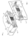
- FIG 1 is a perspective view of an electrical connector assembly 100 formed in accordance with one embodiment.
- the connector assembly 100 includes a sub-assembly 102 that has an electrical component 104 (illustrated as a circuit board 106 in Figure 1 ) and an electrical connector 108 mounted to the circuit board 106.
- the connector assembly 100 also includes another sub-assembly 110 having an electrical component 112, which is illustrated as a circuit board 114, and an electrical connector 116 mounted to the circuit board 114.
- the sub-assemblies 102 and 110 (and corresponding connectors 108 and 116) are configured to mate with one another such that electrical signals and/or power may be transmitted therebetween.
- the connectors 108 and 116 are configured to transmit differential signals.
- the connector 108 includes a plurality of socket members 130 that are sized and shaped to be inserted into corresponding cavities 132 ( Figure 4 ) of the connector 116.
- the cavities 132 hold mating contacts 134 ( Figure 4 ), which, in one embodiment, may be twist pin contacts 236 ( Figure 5 ).
- the socket members 130, cavities 132, and twist pin contacts 236 facilitate maintaining a mechanical and electrical connection between the connectors 108 and 116.
- the following description is with specific reference to the illustrated connectors 108 and 116, alternative embodiments of electrical connectors and assemblies may incorporate similar features and components as described herein. As such, the following description is provided for purposes of illustration, rather than limitation, and is but one potential application of the subject matter herein.
- the connector 108 may be held and covered by a shield 109, and the connector 116 may be held and covered by a shield 115.
- the sub-assemblies 102 and 110 may have additional parts and connectors mounted to the circuit boards 106 and 114, respectively, such as another pair of mateable electrical connectors 117 and 118, complementary guiding features 120 and 122, and power connectors 124 and 126, which are illustrated as DIN power connectors but may be any other type of connector.
- the connector assembly 100 (and corresponding sub-assemblies 102 and 110) may be configured for many applications, such as high-speed telecommunications equipment, various classes of servers, and data storage and transport devices. Also, the connector assembly 100 may be configured to transmit high-speed differential signals. As used herein, the term "high-speed" includes transmission speeds of approximately one (1) gigabit/s or greater. In one embodiment, connectors 108 and 116 are configured to transmit approximately 10 gigabit/s or greater. Furthermore, the connector assembly 100 may perform at high speeds and maintain signal integrity while withstanding vibrations and shock that may be experienced during, for example, aerospace or military operations. As such, the connector assembly 100 may be configured to satisfy known industry standards including military specifications, such as MIL-DTL-83513. However, embodiments described herein are not limited to applications for extreme environments, but may also be used in other environments, such as in an office or home.
- Figure 2 is a partially exploded view of the connector 108
- Figure 3 is an isolated perspective view of a contact module 150A that is used by the connector 108.
- the connector 108 includes a housing assembly 147 that has a plurality of contact modules 150 and a front housing 160.
- the contact modules 150 may be grouped together or arranged to form a contact module assembly 151 ( Figure 2 ) that is held by the front housing 160.
- the various features of the housing assembly 147 and the contact module(s) 150 may be designed to provide an electrical connector, such as the connector 108, that is operable at frequencies, densities, and/or throughputs that are relatively higher than electrical connectors without some or all of the features described herein, by reducing crosstalk, reducing noise persistence, reducing impedance footprint mismatch and/or reducing intra-pair skew.
- each contact module 150 may include a plurality of conductors 152 (shown in Figure 6 ) that extend between a mounting edge 154 and a mating edge 156 of the contact module 150.
- the contact modules 150 also include the socket members 130 that project from the mating edge 156 in a common direction (i.e., parallel with respect to each other).
- the contact modules 150 may be held by the front housing 160 and arranged side-by-side.
- Each contact module 150 may include one shield 158 on one side of the contact module 150. Alternatively, the contact module 150 may have shields on both sides.
- the front housing 160 may include a substantially rectangular and planar mating face 162 and a rear side 164 that engages the contact modules 150.
- the front housing 160 may include a shroud 166 that covers a portion of the contact modules 150.
- An outer surface 168 of the shroud 166 may have features (e.g., ridges, grooves, or keys) for mating with the shield 109.
- the front housing 160 includes a dielectric front portion 170 that extends between the rear side 164 and the mating face 162.
- a plurality of openings or passages 163 extend through the front portion 170 and are configured to receive the socket members 130 when the contact module assembly 151 (or individual contact modules 150) is inserted into the front housing 160.
- the front housing 160 may form open slots that receive and hold the mating edges 156 of each contact module 150.
- the plurality of socket members 130 may project from the mating face 162 in a common direction and at a common distance D.
- the socket members 130 may form a forward-facing array 177, which may take a grid-like form of rows and columns of socket members 130.
- the array 177 of socket members 130 are received by a complementary array 204 ( Figure 4 ) of cavities 132.
- the socket members 130 and cavities 132 may cooperate with other features of the connectors 108 and 116 to facilitate mechanically and electrically coupling the connectors 108 and 116 together.
- FIG 3 illustrates the contact module 150 in greater detail.
- the contact module 150 includes an internal lead frame 180 (shown in Figure 6 ) that includes the conductors 152 ( Figure 6 ) and is contained within a dielectric body 182.
- the lead frame 180 is enclosed within the body 182, but may be partially exposed by the body 182 in certain areas.
- the body 182 is manufactured using an over-molding process.
- the lead frame 180 is encased in a dielectric material, which forms the body 182.
- a plurality of mating tails 186 extend from the mating edge 156 and a plurality of mounting tails 184 extend from the edge 154.
- the mating edge 156 and the mounting edge 154 are generally perpendicular to one another (i.e., the connector 108 is a right-angle connector). Also shown, the body 182 includes opposite side portions 188 and 190 that extend substantially parallel to and along the lead frame 180.
- the contact modules 150 include two different types of contact modules 150 (indicated as 150A and 150B in Figure 2 ) that include different arrangements of conductors 152 ( Figure 6 ) or types of lead frames 180 ( Figure 6 ).
- the contact modules 150A and 150B are placed alongside each other such that side portion 190 of the contact module 150A is adjacent to or abuts the side portion 188 of the contact module 150B.
- the body 182 may include a plurality of openings 192A and 192B formed entirely through the body 182 between the side portions 188 and 190.
- the openings 192A and 192B provide an air gap through the body 182 and may be provided between signal conductors of adjacent differential pairs.
- the openings 192A and 192B may have shapes and lengths that are selected to balance structural integrity of the contact module 150.
- the openings 192A and 192B may provide an air gap between signal conductors, which may decrease the cross-talk of the contact module 150 by providing an air dielectric therebetween as opposed to only a plastic dielectric. Selecting the width and the length of the openings 192A and 192B may balance these factors.
- the openings 192A may be filled with a dielectric material having certain characteristics that may enhance at least one of the stability and the electrical performance of the contact modules 150 and/or module assembly 151.
- the openings 192B are substantially rectangular and arranged near the mounting edge 154 and the mating edge 156 of the contact module 150.
- the openings 192B may be configured to receive grips 193 from the shield 158.
- the grips 192 may attach to and make electrical contact with a ground conductor.
- the mating tails 186 and 184 are compliant pins formed to have an eye-of-needle shape.
- the compliant pins may be configured to form an interference, gas-tight fit with a hole in a circuit board or with a hole 250 (shown in Figure 7 ) of the socket member 130.
- the socket members 130 may include a base portion 131 and a shaft 133.
- the base portion 131 includes the hole 250 through which the mating tail 186 is received and the shaft 133 includes a passage 135 in which the mating contact 134 ( Figure 4 ) is received.
- the diameter of base portion 131 is greater than a diameter of the shaft 133.
- each socket member 130 may be prevented from moving away from the mating edge 156 because the openings 163 of the front housing 160 are configured to prevent movement by the socket member 130.
- Figure 4 is a partially exploded view of the connector 116 that includes a dielectric housing 200 that also has a mating face 202 configured to engage the mating face 162 ( Figure 2 ) of the connector 108 ( Figure 2 ).
- the connector 116 also includes a plurality of cavities 132 that extend through the housing 200.
- the cavities 132 extend linearly through the housing 200 and form a forward-facing array 204 of cavities 132, which may take a complementary grid-like form of rows and columns of cavities 132 with respect to the array 177 of socket members 130.
- the housing 200 may also have an outer surface 206 that surrounds the mating face 202.
- the outer surface 206 and housing 200 may be configured to be surrounded or held by a shield 115 (shown in Figure 6 ).
- the connector also includes a plurality of mating contacts 134 that are inserted into and held by the cavities 132.
- the mating contacts 134 are configured to mate with the socket members 130 ( Figure 1 ) when the socket members 130 are inserted into the cavities 132.
- the mating contact 134 is configured to form multiple points of electrical contact with the shaft 133 ( Figure 3 ) of the socket member 130 ( Figure 3 ).
- Each cavity 132 may have a rounded opening that initially directs the socket members 130 into the corresponding cavity 132.
- the connector 116 may be a vertical-type connector as shown in Figure 4 in that the paths of the mating contacts 134 are substantially linear. However, in alternative embodiments, the connector 116 may be another type of connector.
- Figure 5 is an isolated view of the mating contact 134 and includes a window showing an enlarged, exposed portion of the mating contact 134.
- the mating contact 134 includes a conductive beam 230 having two ends 232 and 234 shaped into compliant pins.
- the beam 230 may have any length or shape in order to transmit signals or power through the connector 116 ( Figure 4 ).
- the compliant pin at the end 232 couples to, for example, the circuit board 114, and the compliant pin at the end 234 is coupled to a twist pin contact 236.
- the twist pin contact 236 includes a barrel 238 that is connected with a plurality of conductive wires 240 that are joined at a core 242.
- the wires 240 are made from a copper material and are helically wound and terminate at a hemispherical weld.
- the wires 240 may form several self wiping spring surfaces that are configured for a consistent continuity and a very low noise level.
- the barrel 238 is configured to form a gas-tight, interference fit with a compliant pin formed by the end 234 of the beam 230.
- the barrel 238 and/or core 242 may also have guiding features on an outer surface thereof. When the mating contact 134 is inserted into the cavity 132 ( Figure 4 ), the guiding features may direct the mating contact 134 into a predetermined position.
- Figure 6 is a perspective cross-sectional view of the connectors 108 and 116 in a fully mated position with each other
- Figure 7 is a cross-sectional view of the engaged connectors 108 and 116 in Figure 6 .
- the connectors 108 and 116 form a mechanical coupling that may withstand extreme temperature, shock, and/or vibrations while maintaining an effective electrical connection.
- the housing assembly 147 and the housing 200 are adjacent to or directly abutting each other.
- the shafts 133 of the socket members 130 are inserted into the corresponding cavities 132 of the connector 116 the distance D ( Figure 2 ).
- the mating contact 134 of the connector 116 are inserted into and covered by the shaft 133 such that the twist pin contact 236 ( Figure 5 ) is electrically connected to the inner surface 252 ( Figure 7 ) of the shaft 133.
- the wires 240 of the twist pin contact 236 form multiple points of electrical contact with the shaft 133 of the socket member 130.
- Figure 7 also illustrates electrical interconnecting portions P1 and P2 formed by the connectors 108 and 116.
- the mating faces 162 and 202 of the connectors 108 and 116, respectively may directly abut each other along an interface I C .
- the mating tail 186 is coupled to and forms an interference fit with the socket member 130
- the end 234 of the beam 230 ( Figure 5 ) is coupled to and forms an interference fit with the twist pin contact 236.
- the shaft 133 of the socket member 130 is inserted into a corresponding cavity 132 of the connector 116.
- the shaft 133 may form an interference or compressive fit within the corresponding cavity 132.
- the wires 240 are deflected into and slide along an inner surface 252 of the socket member 130.
- the wires 240 form multiple points of electrical contact with the inner surface 252.
- the interconnecting portions P1 and P2 cooperate with each other such that the connectors 108 and 116 are mechanically and electrically coupled together.
- the multiple shafts 133 within corresponding cavities 132 may prevent the connectors 108 and 116 from being inadvertently separated along a longitudinal axis 392 (shown in Figure 6 ).
- the multiple points of contact formed by the wires 240 and the shafts 133 facilitate maintaining an electrical connection while the connectors 108 and 116 are sustaining shock and/or vibrations.
- each interconnecting portion P1 and P2 forms an electrical and mechanical coupling.
- embodiments described herein may include electrical connectors that are ruggedized (i.e., built to sustain shock and vibrations and still maintain an effective electrical connection). However, embodiments herein are not limited to such applications. Also, although the illustrated embodiment shows a right-angle connector 108 coupling to a vertical connector 116, the connectors 108 and 116 may take many forms and shapes and the connectors 108 and 116 may couple to each other in many orientations. For example, the connectors 108 and 116 may be incorporated into backplane electrical connector assemblies where the connectors 108 and 116 mate with each other in an orthogonal, coplanar, or mezzanine (stacking) manner.
- the socket members 130 are not separately coupled to the conductors 152 ( Figure 6 ) but are formed with or are an integral part of the conductors 152.
Landscapes
- Details Of Connecting Devices For Male And Female Coupling (AREA)
- Coupling Device And Connection With Printed Circuit (AREA)
- Connector Housings Or Holding Contact Members (AREA)
Claims (10)
- Elektrische Verbinderanordnung (100) für das Verbinden eines ersten und zweiten elektrischen Bauteils (112, 104), wobei die Verbinderanordnung (100) aufweist:einen Gegensteckverbinder (116), der ein Gehäuse (200) mit einer Eingriffsfläche (202) und einer Vielzahl von Hohlräumen (132) aufweist, die sich in das Gehäuse (200) hinein erstrecken, wobei ein jeder Hohlraum (132) einen Gegenkontakt (134) darin aufweist, der elektrisch mit dem ersten elektrischen Bauteil (112) verbunden ist; undeinen Buchsenverbinder (108), der ausgebildet ist, um mit dem Gegensteckverbinder (116) in Eingriff zu kommen, wobei der Buchsenverbinder (108) aufweist:ein Buchsengehäuse (147) mit einer Eingriffsfläche (162), die ausgebildet ist, um mit der Eingriffsfläche (202) des Gegensteckverbinders (116) in Eingriff zu kommen;eine Vielzahl von Leitern (152), die sich durch das Buchsengehäuse (147) erstrecken und elektrisch mit dem zweiten elektrischen Bauteil (104) verbunden sind; undeine Vielzahl von Buchsenelementen (130), die elektrisch mit den Leitern (152) verbunden sind, wobei ein jedes Buchsenelement (130) eine Welle (133) aufweist, die aus der Eingriffsfläche (162) des Buchsengehäuses (147) vorsteht und für ein Einsetzen in einen der Hohlräume (132) ausgebildet ist, unddadurch gekennzeichnet, dass die Welle (133) einen Durchgang bildet, der für das Aufnehmen des innerhalb des Hohlraumes (132) gehaltenen entsprechenden Gegenkontaktes (134) ausgebildet ist, um eine elektrische Verbindung zwischen dem entsprechenden Gegenkontakt und der Welle zu bewirken.
- Verbinderanordnung (100) nach Anspruch 1, bei der die Gegenkontakte (134) ausgebildet sind, um mehrere elektrische Kontaktpunkte innerhalb der Welle (133) des Buchsenelementes (130) zu bewirken.
- Verbinderanordnung (100) nach Anspruch 2, bei der die Gegenkontakte (134) Twist-Pin Kontakte sind.
- Verbinderanordnung (100) nach Anspruch 1, bei der die Vielzahl der Buchsenelemente (130) in einer Anordnung (177) ausgebildet ist, die Reihen und senkrechte Reihen von Buchsenelementen (130) umfasst, die aus der Eingriffsfläche (162) in einer gemeinsamen Richtung herausragen.
- Verbinderanordnung (100) nach Anspruch 1, bei der die Eingriffsfläche (162) im Wesentlichen eben ist, wobei die Buchsenelemente (130) aus der Eingriffsfläche (162) in einer gemeinsamen Richtung herausragen.
- Verbinderanordnung (100) nach Anspruch 1, bei der die Leiter (152) ein hinteres Eingriffsende (186) mit einem nachgiebigen Stift (184) umfassen, und bei der das Buchsenelement (130) ein Loch (250) für das Aufnehmen des nachgiebigen Stiftes (184) umfasst, wobei das Buchsenelement (130) und der nachgiebige Stift (184) eine Presspassung miteinander bilden, so dass das Buchsenelement (130) und der nachgiebige Stift (184) mechanisch und elektrisch miteinander verbunden werden.
- Verbinderanordnung (100) nach Anspruch 1, bei der das Gehäuse (147) einen Stecksockel (160) mit einer Eingriffsfläche (162) darauf umfasst, wobei der Stecksockel (160) Öffnungen (163) aufweist, wobei sich die Buchsenelemente (130) durch den Stecksockel (160) hindurch erstrecken und von ihm weg vorstehen.
- Verbinderanordnung (100) nach Anspruch 1, bei der das Gehäuse (147) außerdem einen Stecksockel (160) mit einer Eingriffsfläche (162) darauf und einer Vielzahl von Kontaktmodulen (150) aufweist, wobei ein jedes Kontaktmodul (150) benachbart einem weiteren Kontaktmodul (150) gehalten und mit dem Stecksockel (160) verbunden wird.
- Verbinderanordnung (100) nach Anspruch 1, bei der das Gehäuse (147) und die Leiter (152) ausgebildet sind, um Hochleistungsdifferentialsignale zu übertragen.
- Verbinderanordnung (100) nach Anspruch 1, bei der das Gehäuse (147) so ausgebildet ist, dass es auf eine Leiterplatte (106) montiert werden kann, wobei sich die Leiter (152) durch das Gehäuse (147) erstrecken und mit der Leiterplatte (106) verbinden.
Applications Claiming Priority (2)
| Application Number | Priority Date | Filing Date | Title |
|---|---|---|---|
| US12/177,646 US7867045B2 (en) | 2008-07-22 | 2008-07-22 | Electrical connectors and assemblies having socket members |
| PCT/US2009/004252 WO2010011309A1 (en) | 2008-07-22 | 2009-07-22 | Electrical connectors and assemblies having socket members |
Publications (2)
| Publication Number | Publication Date |
|---|---|
| EP2321880A1 EP2321880A1 (de) | 2011-05-18 |
| EP2321880B1 true EP2321880B1 (de) | 2015-05-06 |
Family
ID=41020968
Family Applications (1)
| Application Number | Title | Priority Date | Filing Date |
|---|---|---|---|
| EP20090788976 Active EP2321880B1 (de) | 2008-07-22 | 2009-07-22 | Elektrische verbinder und baugruppen mit buchsenkontakt |
Country Status (4)
| Country | Link |
|---|---|
| US (1) | US7867045B2 (de) |
| EP (1) | EP2321880B1 (de) |
| CN (1) | CN102106042B (de) |
| WO (1) | WO2010011309A1 (de) |
Cited By (1)
| Publication number | Priority date | Publication date | Assignee | Title |
|---|---|---|---|---|
| US20210384674A1 (en) * | 2020-06-09 | 2021-12-09 | Afag Holding Ag | Electrical connecting device having a main body and a displacement body |
Families Citing this family (9)
| Publication number | Priority date | Publication date | Assignee | Title |
|---|---|---|---|---|
| CN104779499A (zh) * | 2012-01-04 | 2015-07-15 | 凡甲电子(苏州)有限公司 | 电连接器 |
| US9136652B2 (en) * | 2012-02-07 | 2015-09-15 | Fci Americas Technology Llc | Electrical connector assembly |
| US9362693B2 (en) * | 2014-01-14 | 2016-06-07 | Tyco Electronics Corporation | Header assembly having power and signal cartridges |
| CN205070095U (zh) * | 2015-09-15 | 2016-03-02 | 富士康(昆山)电脑接插件有限公司 | 电连接器 |
| US9742081B1 (en) * | 2016-05-24 | 2017-08-22 | Te Connectivity Corporation | Press-fit circuit board connector |
| WO2018092068A1 (en) * | 2016-11-16 | 2018-05-24 | Te Connectivity Corporation | Press-fit circuit board connector |
| US9930780B1 (en) | 2016-11-22 | 2018-03-27 | Lear Corporation | Remote control device having motherboard and battery daughterboard connected by interconnect |
| US10770839B2 (en) * | 2018-08-22 | 2020-09-08 | Amphenol Corporation | Assembly method for a printed circuit board electrical connector |
| CN110891369A (zh) * | 2018-09-07 | 2020-03-17 | 富加宜(美国)有限责任公司 | 低成本高速印刷电路板的连接器 |
Family Cites Families (15)
| Publication number | Priority date | Publication date | Assignee | Title |
|---|---|---|---|---|
| US3716817A (en) * | 1971-04-21 | 1973-02-13 | Mc Donnell Douglas Corp | Electrical connectors |
| GB1530786A (en) * | 1974-12-30 | 1978-11-01 | Trw Inc | Electrical connector |
| US4170393A (en) * | 1977-11-14 | 1979-10-09 | Power Industries Inc., Division of Groman Corporation | Electrical connector with replaceable contacts |
| US4193655A (en) * | 1978-07-20 | 1980-03-18 | Amp Incorporated | Field repairable connector assembly |
| US4311355A (en) * | 1978-10-23 | 1982-01-19 | General Motors Corporation | Weatherproof electrical connector |
| US4944686A (en) * | 1989-05-01 | 1990-07-31 | Audio Authority Corporation | Solderless electrical connector |
| US5051108A (en) * | 1990-03-19 | 1991-09-24 | Microdot Inc. | Connector |
| US5133679A (en) * | 1990-06-08 | 1992-07-28 | E. I. Du Pont De Nemours And Company | Connectors with ground structure |
| US5194020A (en) * | 1991-06-17 | 1993-03-16 | W. L. Gore & Associates, Inc. | High-density coaxial interconnect system |
| FR2702095B1 (fr) * | 1993-02-26 | 1995-04-14 | Radiall Sa | Elément coudé de connecteur coaxial apte à être fixé à une carte imprimée. |
| US5362261A (en) * | 1993-06-30 | 1994-11-08 | The Whitaker Corporation | Hybrid connector |
| US5588852A (en) * | 1995-03-21 | 1996-12-31 | The Whitaker Corporation | Electrical connector having socket contacts with safety shields |
| US5842872A (en) * | 1995-06-30 | 1998-12-01 | The Whitaker Corporation | Modular right angle board mountable coaxial connector |
| US6116931A (en) * | 1997-11-10 | 2000-09-12 | The Whitaker Corporation | Contact array for electrical interface connector |
| US7384311B2 (en) * | 2006-02-27 | 2008-06-10 | Tyco Electronics Corporation | Electrical connector having contact modules with terminal exposing slots |
-
2008
- 2008-07-22 US US12/177,646 patent/US7867045B2/en active Active
-
2009
- 2009-07-22 CN CN200980128548.1A patent/CN102106042B/zh active Active
- 2009-07-22 WO PCT/US2009/004252 patent/WO2010011309A1/en active Application Filing
- 2009-07-22 EP EP20090788976 patent/EP2321880B1/de active Active
Cited By (2)
| Publication number | Priority date | Publication date | Assignee | Title |
|---|---|---|---|---|
| US20210384674A1 (en) * | 2020-06-09 | 2021-12-09 | Afag Holding Ag | Electrical connecting device having a main body and a displacement body |
| US11621524B2 (en) * | 2020-06-09 | 2023-04-04 | Afag Holdingag | Electrical connecting device having a main body and a displacement body |
Also Published As
| Publication number | Publication date |
|---|---|
| US7867045B2 (en) | 2011-01-11 |
| US20100022142A1 (en) | 2010-01-28 |
| EP2321880A1 (de) | 2011-05-18 |
| CN102106042B (zh) | 2013-10-23 |
| WO2010011309A1 (en) | 2010-01-28 |
| CN102106042A (zh) | 2011-06-22 |
Similar Documents
| Publication | Publication Date | Title |
|---|---|---|
| EP2321880B1 (de) | Elektrische verbinder und baugruppen mit buchsenkontakt | |
| US11715914B2 (en) | High speed, high density electrical connector with shielded signal paths | |
| US7909668B2 (en) | Contact with twist pin interface | |
| US6910897B2 (en) | Interconnection system | |
| US7901238B1 (en) | Terminal block and board assembly for an electrical connector | |
| US9531129B2 (en) | Electrical connector and connector system having bussed ground conductors | |
| EP1719210B1 (de) | Verbindervorrichtung | |
| US7004793B2 (en) | Low inductance shielded connector | |
| KR100808728B1 (ko) | 고속 커넥터 | |
| US20060105636A1 (en) | Modular coaxial electrical interconnect system and method of making the same | |
| US9490586B1 (en) | Electrical connector having a ground shield | |
| US11909147B2 (en) | Cable connector assembly | |
| US10181670B2 (en) | Connector sub-assembly and electrical connector having signal and ground conductors |
Legal Events
| Date | Code | Title | Description |
|---|---|---|---|
| PUAI | Public reference made under article 153(3) epc to a published international application that has entered the european phase |
Free format text: ORIGINAL CODE: 0009012 |
|
| 17P | Request for examination filed |
Effective date: 20110216 |
|
| AK | Designated contracting states |
Kind code of ref document: A1 Designated state(s): AT BE BG CH CY CZ DE DK EE ES FI FR GB GR HR HU IE IS IT LI LT LU LV MC MK MT NL NO PL PT RO SE SI SK SM TR |
|
| AX | Request for extension of the european patent |
Extension state: AL BA RS |
|
| DAX | Request for extension of the european patent (deleted) | ||
| REG | Reference to a national code |
Ref country code: DE Ref legal event code: R079 Ref document number: 602009031141 Country of ref document: DE Free format text: PREVIOUS MAIN CLASS: H01R0013646000 Ipc: H01R0013050000 |
|
| RIC1 | Information provided on ipc code assigned before grant |
Ipc: H01R 13/05 20060101AFI20141020BHEP Ipc: H01R 13/33 20060101ALI20141020BHEP Ipc: H01R 12/50 20110101ALI20141020BHEP Ipc: H01R 13/10 20060101ALI20141020BHEP |
|
| GRAP | Despatch of communication of intention to grant a patent |
Free format text: ORIGINAL CODE: EPIDOSNIGR1 |
|
| INTG | Intention to grant announced |
Effective date: 20141203 |
|
| GRAS | Grant fee paid |
Free format text: ORIGINAL CODE: EPIDOSNIGR3 |
|
| GRAA | (expected) grant |
Free format text: ORIGINAL CODE: 0009210 |
|
| AK | Designated contracting states |
Kind code of ref document: B1 Designated state(s): AT BE BG CH CY CZ DE DK EE ES FI FR GB GR HR HU IE IS IT LI LT LU LV MC MK MT NL NO PL PT RO SE SI SK SM TR |
|
| REG | Reference to a national code |
Ref country code: GB Ref legal event code: FG4D |
|
| REG | Reference to a national code |
Ref country code: CH Ref legal event code: EP |
|
| REG | Reference to a national code |
Ref country code: IE Ref legal event code: FG4D |
|
| REG | Reference to a national code |
Ref country code: AT Ref legal event code: REF Ref document number: 726261 Country of ref document: AT Kind code of ref document: T Effective date: 20150615 |
|
| REG | Reference to a national code |
Ref country code: DE Ref legal event code: R096 Ref document number: 602009031141 Country of ref document: DE Effective date: 20150618 |
|
| REG | Reference to a national code |
Ref country code: AT Ref legal event code: MK05 Ref document number: 726261 Country of ref document: AT Kind code of ref document: T Effective date: 20150506 |
|
| REG | Reference to a national code |
Ref country code: NL Ref legal event code: MP Effective date: 20150506 |
|
| REG | Reference to a national code |
Ref country code: LT Ref legal event code: MG4D |
|
| PG25 | Lapsed in a contracting state [announced via postgrant information from national office to epo] |
Ref country code: ES Free format text: LAPSE BECAUSE OF FAILURE TO SUBMIT A TRANSLATION OF THE DESCRIPTION OR TO PAY THE FEE WITHIN THE PRESCRIBED TIME-LIMIT Effective date: 20150506 Ref country code: LT Free format text: LAPSE BECAUSE OF FAILURE TO SUBMIT A TRANSLATION OF THE DESCRIPTION OR TO PAY THE FEE WITHIN THE PRESCRIBED TIME-LIMIT Effective date: 20150506 Ref country code: NO Free format text: LAPSE BECAUSE OF FAILURE TO SUBMIT A TRANSLATION OF THE DESCRIPTION OR TO PAY THE FEE WITHIN THE PRESCRIBED TIME-LIMIT Effective date: 20150806 Ref country code: PT Free format text: LAPSE BECAUSE OF FAILURE TO SUBMIT A TRANSLATION OF THE DESCRIPTION OR TO PAY THE FEE WITHIN THE PRESCRIBED TIME-LIMIT Effective date: 20150907 Ref country code: HR Free format text: LAPSE BECAUSE OF FAILURE TO SUBMIT A TRANSLATION OF THE DESCRIPTION OR TO PAY THE FEE WITHIN THE PRESCRIBED TIME-LIMIT Effective date: 20150506 Ref country code: FI Free format text: LAPSE BECAUSE OF FAILURE TO SUBMIT A TRANSLATION OF THE DESCRIPTION OR TO PAY THE FEE WITHIN THE PRESCRIBED TIME-LIMIT Effective date: 20150506 |
|
| PG25 | Lapsed in a contracting state [announced via postgrant information from national office to epo] |
Ref country code: GR Free format text: LAPSE BECAUSE OF FAILURE TO SUBMIT A TRANSLATION OF THE DESCRIPTION OR TO PAY THE FEE WITHIN THE PRESCRIBED TIME-LIMIT Effective date: 20150807 Ref country code: LV Free format text: LAPSE BECAUSE OF FAILURE TO SUBMIT A TRANSLATION OF THE DESCRIPTION OR TO PAY THE FEE WITHIN THE PRESCRIBED TIME-LIMIT Effective date: 20150506 Ref country code: AT Free format text: LAPSE BECAUSE OF FAILURE TO SUBMIT A TRANSLATION OF THE DESCRIPTION OR TO PAY THE FEE WITHIN THE PRESCRIBED TIME-LIMIT Effective date: 20150506 Ref country code: IS Free format text: LAPSE BECAUSE OF FAILURE TO SUBMIT A TRANSLATION OF THE DESCRIPTION OR TO PAY THE FEE WITHIN THE PRESCRIBED TIME-LIMIT Effective date: 20150906 Ref country code: BG Free format text: LAPSE BECAUSE OF FAILURE TO SUBMIT A TRANSLATION OF THE DESCRIPTION OR TO PAY THE FEE WITHIN THE PRESCRIBED TIME-LIMIT Effective date: 20150806 |
|
| PG25 | Lapsed in a contracting state [announced via postgrant information from national office to epo] |
Ref country code: EE Free format text: LAPSE BECAUSE OF FAILURE TO SUBMIT A TRANSLATION OF THE DESCRIPTION OR TO PAY THE FEE WITHIN THE PRESCRIBED TIME-LIMIT Effective date: 20150506 Ref country code: DK Free format text: LAPSE BECAUSE OF FAILURE TO SUBMIT A TRANSLATION OF THE DESCRIPTION OR TO PAY THE FEE WITHIN THE PRESCRIBED TIME-LIMIT Effective date: 20150506 |
|
| REG | Reference to a national code |
Ref country code: DE Ref legal event code: R097 Ref document number: 602009031141 Country of ref document: DE |
|
| PG25 | Lapsed in a contracting state [announced via postgrant information from national office to epo] |
Ref country code: SK Free format text: LAPSE BECAUSE OF FAILURE TO SUBMIT A TRANSLATION OF THE DESCRIPTION OR TO PAY THE FEE WITHIN THE PRESCRIBED TIME-LIMIT Effective date: 20150506 Ref country code: CZ Free format text: LAPSE BECAUSE OF FAILURE TO SUBMIT A TRANSLATION OF THE DESCRIPTION OR TO PAY THE FEE WITHIN THE PRESCRIBED TIME-LIMIT Effective date: 20150506 Ref country code: RO Free format text: LAPSE BECAUSE OF NON-PAYMENT OF DUE FEES Effective date: 20150506 Ref country code: PL Free format text: LAPSE BECAUSE OF FAILURE TO SUBMIT A TRANSLATION OF THE DESCRIPTION OR TO PAY THE FEE WITHIN THE PRESCRIBED TIME-LIMIT Effective date: 20150506 Ref country code: MC Free format text: LAPSE BECAUSE OF FAILURE TO SUBMIT A TRANSLATION OF THE DESCRIPTION OR TO PAY THE FEE WITHIN THE PRESCRIBED TIME-LIMIT Effective date: 20150506 |
|
| REG | Reference to a national code |
Ref country code: CH Ref legal event code: PL |
|
| PLBE | No opposition filed within time limit |
Free format text: ORIGINAL CODE: 0009261 |
|
| STAA | Information on the status of an ep patent application or granted ep patent |
Free format text: STATUS: NO OPPOSITION FILED WITHIN TIME LIMIT |
|
| PG25 | Lapsed in a contracting state [announced via postgrant information from national office to epo] |
Ref country code: LU Free format text: LAPSE BECAUSE OF FAILURE TO SUBMIT A TRANSLATION OF THE DESCRIPTION OR TO PAY THE FEE WITHIN THE PRESCRIBED TIME-LIMIT Effective date: 20150722 |
|
| 26N | No opposition filed |
Effective date: 20160209 |
|
| REG | Reference to a national code |
Ref country code: IE Ref legal event code: MM4A |
|
| PG25 | Lapsed in a contracting state [announced via postgrant information from national office to epo] |
Ref country code: CH Free format text: LAPSE BECAUSE OF NON-PAYMENT OF DUE FEES Effective date: 20150731 Ref country code: IT Free format text: LAPSE BECAUSE OF FAILURE TO SUBMIT A TRANSLATION OF THE DESCRIPTION OR TO PAY THE FEE WITHIN THE PRESCRIBED TIME-LIMIT Effective date: 20150506 Ref country code: LI Free format text: LAPSE BECAUSE OF NON-PAYMENT OF DUE FEES Effective date: 20150731 |
|
| PG25 | Lapsed in a contracting state [announced via postgrant information from national office to epo] |
Ref country code: SI Free format text: LAPSE BECAUSE OF FAILURE TO SUBMIT A TRANSLATION OF THE DESCRIPTION OR TO PAY THE FEE WITHIN THE PRESCRIBED TIME-LIMIT Effective date: 20150506 |
|
| REG | Reference to a national code |
Ref country code: FR Ref legal event code: PLFP Year of fee payment: 8 |
|
| PG25 | Lapsed in a contracting state [announced via postgrant information from national office to epo] |
Ref country code: IE Free format text: LAPSE BECAUSE OF NON-PAYMENT OF DUE FEES Effective date: 20150722 |
|
| PG25 | Lapsed in a contracting state [announced via postgrant information from national office to epo] |
Ref country code: BE Free format text: LAPSE BECAUSE OF FAILURE TO SUBMIT A TRANSLATION OF THE DESCRIPTION OR TO PAY THE FEE WITHIN THE PRESCRIBED TIME-LIMIT Effective date: 20150506 |
|
| PG25 | Lapsed in a contracting state [announced via postgrant information from national office to epo] |
Ref country code: MT Free format text: LAPSE BECAUSE OF FAILURE TO SUBMIT A TRANSLATION OF THE DESCRIPTION OR TO PAY THE FEE WITHIN THE PRESCRIBED TIME-LIMIT Effective date: 20150506 |
|
| PG25 | Lapsed in a contracting state [announced via postgrant information from national office to epo] |
Ref country code: SM Free format text: LAPSE BECAUSE OF FAILURE TO SUBMIT A TRANSLATION OF THE DESCRIPTION OR TO PAY THE FEE WITHIN THE PRESCRIBED TIME-LIMIT Effective date: 20150506 Ref country code: HU Free format text: LAPSE BECAUSE OF FAILURE TO SUBMIT A TRANSLATION OF THE DESCRIPTION OR TO PAY THE FEE WITHIN THE PRESCRIBED TIME-LIMIT; INVALID AB INITIO Effective date: 20090722 |
|
| PG25 | Lapsed in a contracting state [announced via postgrant information from national office to epo] |
Ref country code: NL Free format text: LAPSE BECAUSE OF FAILURE TO SUBMIT A TRANSLATION OF THE DESCRIPTION OR TO PAY THE FEE WITHIN THE PRESCRIBED TIME-LIMIT Effective date: 20150506 Ref country code: SE Free format text: LAPSE BECAUSE OF FAILURE TO SUBMIT A TRANSLATION OF THE DESCRIPTION OR TO PAY THE FEE WITHIN THE PRESCRIBED TIME-LIMIT Effective date: 20150506 Ref country code: CY Free format text: LAPSE BECAUSE OF FAILURE TO SUBMIT A TRANSLATION OF THE DESCRIPTION OR TO PAY THE FEE WITHIN THE PRESCRIBED TIME-LIMIT Effective date: 20150506 |
|
| REG | Reference to a national code |
Ref country code: FR Ref legal event code: PLFP Year of fee payment: 9 |
|
| PG25 | Lapsed in a contracting state [announced via postgrant information from national office to epo] |
Ref country code: TR Free format text: LAPSE BECAUSE OF FAILURE TO SUBMIT A TRANSLATION OF THE DESCRIPTION OR TO PAY THE FEE WITHIN THE PRESCRIBED TIME-LIMIT Effective date: 20150506 |
|
| REG | Reference to a national code |
Ref country code: FR Ref legal event code: PLFP Year of fee payment: 10 |
|
| PG25 | Lapsed in a contracting state [announced via postgrant information from national office to epo] |
Ref country code: MK Free format text: LAPSE BECAUSE OF FAILURE TO SUBMIT A TRANSLATION OF THE DESCRIPTION OR TO PAY THE FEE WITHIN THE PRESCRIBED TIME-LIMIT Effective date: 20150506 |
|
| REG | Reference to a national code |
Ref country code: FR Ref legal event code: CD Owner name: TYCO ELECTRONICS CORPORATION, US Effective date: 20180626 |
|
| REG | Reference to a national code |
Ref country code: DE Ref legal event code: R082 Ref document number: 602009031141 Country of ref document: DE Representative=s name: MARKS & CLERK (LUXEMBOURG) LLP, LU Ref country code: DE Ref legal event code: R081 Ref document number: 602009031141 Country of ref document: DE Owner name: TE CONNECTIVITY CORPORATION, BERWYN, US Free format text: FORMER OWNER: TYCO ELECTRONICS CORP., BERWYN, PA., US |
|
| PGFP | Annual fee paid to national office [announced via postgrant information from national office to epo] |
Ref country code: FR Payment date: 20230608 Year of fee payment: 15 |
|
| PGFP | Annual fee paid to national office [announced via postgrant information from national office to epo] |
Ref country code: GB Payment date: 20230601 Year of fee payment: 15 |
|
| PGFP | Annual fee paid to national office [announced via postgrant information from national office to epo] |
Ref country code: DE Payment date: 20230531 Year of fee payment: 15 |