EP2320552B1 - Control method for an apparatus converting direct current into alternating current - Google Patents
Control method for an apparatus converting direct current into alternating current Download PDFInfo
- Publication number
- EP2320552B1 EP2320552B1 EP08787613.2A EP08787613A EP2320552B1 EP 2320552 B1 EP2320552 B1 EP 2320552B1 EP 08787613 A EP08787613 A EP 08787613A EP 2320552 B1 EP2320552 B1 EP 2320552B1
- Authority
- EP
- European Patent Office
- Prior art keywords
- stage
- current
- controlling
- converting direct
- direct current
- Prior art date
- Legal status (The legal status is an assumption and is not a legal conclusion. Google has not performed a legal analysis and makes no representation as to the accuracy of the status listed.)
- Active
Links
Images


Classifications
-
- H—ELECTRICITY
- H02—GENERATION; CONVERSION OR DISTRIBUTION OF ELECTRIC POWER
- H02M—APPARATUS FOR CONVERSION BETWEEN AC AND AC, BETWEEN AC AND DC, OR BETWEEN DC AND DC, AND FOR USE WITH MAINS OR SIMILAR POWER SUPPLY SYSTEMS; CONVERSION OF DC OR AC INPUT POWER INTO SURGE OUTPUT POWER; CONTROL OR REGULATION THEREOF
- H02M7/00—Conversion of AC power input into DC power output; Conversion of DC power input into AC power output
- H02M7/42—Conversion of DC power input into AC power output without possibility of reversal
- H02M7/44—Conversion of DC power input into AC power output without possibility of reversal by static converters
- H02M7/48—Conversion of DC power input into AC power output without possibility of reversal by static converters using discharge tubes with control electrode or semiconductor devices with control electrode
- H02M7/53—Conversion of DC power input into AC power output without possibility of reversal by static converters using discharge tubes with control electrode or semiconductor devices with control electrode using devices of a triode or transistor type requiring continuous application of a control signal
- H02M7/537—Conversion of DC power input into AC power output without possibility of reversal by static converters using discharge tubes with control electrode or semiconductor devices with control electrode using devices of a triode or transistor type requiring continuous application of a control signal using semiconductor devices only, e.g. single switched pulse inverters
- H02M7/538—Conversion of DC power input into AC power output without possibility of reversal by static converters using discharge tubes with control electrode or semiconductor devices with control electrode using devices of a triode or transistor type requiring continuous application of a control signal using semiconductor devices only, e.g. single switched pulse inverters in a push-pull configuration
- H02M7/53803—Conversion of DC power input into AC power output without possibility of reversal by static converters using discharge tubes with control electrode or semiconductor devices with control electrode using devices of a triode or transistor type requiring continuous application of a control signal using semiconductor devices only, e.g. single switched pulse inverters in a push-pull configuration with automatic control of output voltage or current
-
- H—ELECTRICITY
- H02—GENERATION; CONVERSION OR DISTRIBUTION OF ELECTRIC POWER
- H02M—APPARATUS FOR CONVERSION BETWEEN AC AND AC, BETWEEN AC AND DC, OR BETWEEN DC AND DC, AND FOR USE WITH MAINS OR SIMILAR POWER SUPPLY SYSTEMS; CONVERSION OF DC OR AC INPUT POWER INTO SURGE OUTPUT POWER; CONTROL OR REGULATION THEREOF
- H02M7/00—Conversion of AC power input into DC power output; Conversion of DC power input into AC power output
- H02M7/42—Conversion of DC power input into AC power output without possibility of reversal
- H02M7/44—Conversion of DC power input into AC power output without possibility of reversal by static converters
- H02M7/48—Conversion of DC power input into AC power output without possibility of reversal by static converters using discharge tubes with control electrode or semiconductor devices with control electrode
- H02M7/53—Conversion of DC power input into AC power output without possibility of reversal by static converters using discharge tubes with control electrode or semiconductor devices with control electrode using devices of a triode or transistor type requiring continuous application of a control signal
- H02M7/537—Conversion of DC power input into AC power output without possibility of reversal by static converters using discharge tubes with control electrode or semiconductor devices with control electrode using devices of a triode or transistor type requiring continuous application of a control signal using semiconductor devices only, e.g. single switched pulse inverters
- H02M7/539—Conversion of DC power input into AC power output without possibility of reversal by static converters using discharge tubes with control electrode or semiconductor devices with control electrode using devices of a triode or transistor type requiring continuous application of a control signal using semiconductor devices only, e.g. single switched pulse inverters with automatic control of output wave form or frequency
- H02M7/5395—Conversion of DC power input into AC power output without possibility of reversal by static converters using discharge tubes with control electrode or semiconductor devices with control electrode using devices of a triode or transistor type requiring continuous application of a control signal using semiconductor devices only, e.g. single switched pulse inverters with automatic control of output wave form or frequency by pulse-width modulation
-
- Y—GENERAL TAGGING OF NEW TECHNOLOGICAL DEVELOPMENTS; GENERAL TAGGING OF CROSS-SECTIONAL TECHNOLOGIES SPANNING OVER SEVERAL SECTIONS OF THE IPC; TECHNICAL SUBJECTS COVERED BY FORMER USPC CROSS-REFERENCE ART COLLECTIONS [XRACs] AND DIGESTS
- Y02—TECHNOLOGIES OR APPLICATIONS FOR MITIGATION OR ADAPTATION AGAINST CLIMATE CHANGE
- Y02E—REDUCTION OF GREENHOUSE GAS [GHG] EMISSIONS, RELATED TO ENERGY GENERATION, TRANSMISSION OR DISTRIBUTION
- Y02E10/00—Energy generation through renewable energy sources
- Y02E10/50—Photovoltaic [PV] energy
- Y02E10/56—Power conversion systems, e.g. maximum power point trackers
Definitions
- the invention provides a control method applicable to DC/AC (direct current / alternating current) conversion structures, specially designed for photovoltaic systems, aimed at enhancing conversion structure efficiency.
- the invention can also be applicable to other fields of energy generation, such as energy generation by means of electrochemical cells or wind energy.
- photovoltaic systems are widely acknowledged in our society. They are facilities formed by a set of photovoltaic panels (photovoltaic field) and an electronic converter that transforms the energy produced by the panels for injection into the electricity grid or load feeding, depending on whether they are grid-connected facilities or isolated systems.
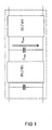
- FIG. 1 shows a schematic view of a photovoltaic converter formed by the union between a DC/DC stage and a DC/AC stage.
- a capacity (C bus ) is disposed between the two stages in the so-called continuous bus for the purpose of stabilising DC/DC stage output voltage. Said voltage is called bus voltage (V bus ).
- Both the DC/DC stage and DC/AC stage are controlled by control loops that vary in function between isolated facilities or grid-connected facilities:
- the respective control loops will determine the instructions introduced into the modulator of each stage to establish the power on/power off orders of the different transistors that constitute the stage.
- the modulators used are normally of the PWM (Pulse Width Modulation) or vector type.
- the bus voltage value required is determined by: the type of DC/AC conversion structure used, grid voltage value or sinusoidal voltage in the case of isolated systems and voltage dip during converter inductance.
- the minimum voltage applied by the DC/AC inverter output stage (V inv,min ) must be greater than the sum of the grid voltage peak value (or sinusoidal output voltage in isolated systems) ( V ⁇ grid ), and voltage dip during converter inductance (V L ), as shown in figure 2 .
- V busref,min K ⁇ V ⁇ grid 2 + V L 2
- K is a constant that depends on the conversion topology used.
- the bus voltage reference value normally increases with respect to the minimum value indicated in the preceding cases.
- leeway is allowed during possible transitories, while simultaneously enhancing grid injection current quality.
- Grid injection current quality is evaluated based on THD (Total Harmonic Distorsion), a factor that measures harmonic amplitude with respect to the fundamental harmonic.
- THD Total Harmonic Distorsion
- Figure 4 shows, by way of example, the evolution of coil current evolution (L/2) and H-bridge monophasic DC/AC stage output voltage, functioning according to the previously expounded method of the state of art, for a reference bus voltage 10% higher than the grid voltage peak value.
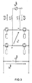
- a DC/AC structure commonly used in photovoltaic converters is the H-bridge ( figure 3 ) with unipolar PWM modulation, said structure having demonstrated a good efficiency/complexity ratio.
- DC/AC conversion topologies with less losses have been developed, such as those disclosed in EP1369985 , US2005286281 or WO2008015298A1 . These topologies enhance the efficiency of the DC/AC structure but increase the complexity of the conversion structure.
- the present invention corresponds to a control method applicable to DC/AC conversion structures, particularly applicable to electronic converters for photovoltaic systems and more specifically to conversion structures formed by combining one or several DC/DC stages with one or several DC/AC stages.
- the proposed control method reduces semiconductor switching losses, enhancing conversion structure efficiency.
- the invention is also applicable in other fields of energy generation wherein DC/AC conversion structures are used, such as energy generation by means of electrochemical cells or wind energy.
- the present invention proposes the implementation of a new control method in the electronic converter formed by at least one DC/AC stage with its respective control loops.
- Said control method comprises the following phases:
- a new control loop regulates the bus voltage reference value.
- This loop is in charge of calculating the value of said voltage based on the pre-set harmonic current distortion. By establishing a distortion value greater than that obtained without modulator saturation, this new loop will cause the modulator to become controllably saturated during grid voltage maximums.
- Modulator saturation produces a deformation in output current and therefore an increase in current THD with respect to the state of the art.
- the proposed control method controls the THD value, guaranteeing a pre-set value at all times.
- the relationship between current THD and modulator saturation time allows calculation of the bus voltage reference value, by means of a regulator that controls the saturation time of each DC/AC stage for a determined period of time. Said period of time may be a multiple or sub-multiple of the grid voltage.
- a voltage control loop determines the output current amplitude of each DC/AC stage. Subsequently, at least one current control loop of each DC/AC stage determines the reference introduced into the modulator of each DC/AC stage.
- the invention envisages the case where there is at least one DC/DC input stage, controlling bus voltage by means of said stage.
- a voltage control loop determines current amplitude of the DC/DC stages.
- at least one current control loop of each DC/DC stage determines the reference that is introduced into the modulator of each DC/AC stage.
- the aforementioned DC/AC stages may be of the monophasic or triphasic type. Additionally, they may be of the multi-level type.
- the invention is also applicable in other fields of energy generation, such as energy generation by means of electrochemical cells or wind energy
- FIG. 5 shows a preferred embodiment of the proposed control method.
- the bus voltage reference value ( V bus ref ) is calculated based on the currentTHD error and grid voltage value.
- FIG. 6 shows a second preferred embodiment of the proposed control method, based on the relationship between current THD and modulator saturation time.
- the bus voltage reference value ( V bus ref ) is obtained from a regulator ( Reg ) that controls modulator saturation time by grid period, taking the error in saturation times and grid voltage value ( V bus ref ), into account.
- Figure 7 shows, by way of example, the evolution of the coil (L) current I (L) and output voltage (VAB) of an H-bridge monophasic DC/AC stage with unipolar PWM modulation after applying the proposed control method.
- the proposed control method enhances converter efficiency by reducing bus voltage and suppressing switching.
- a bus voltage control loop that determines the amplitude of each output current of each DC/AC stage is incorporated.
- Another preferred embodiment is characterised by incorporating at least one current control loop that determines each reference introduced into the modulator.
Landscapes
- Engineering & Computer Science (AREA)
- Power Engineering (AREA)
- Inverter Devices (AREA)
- Dc-Dc Converters (AREA)
Description
- The invention provides a control method applicable to DC/AC (direct current / alternating current) conversion structures, specially designed for photovoltaic systems, aimed at enhancing conversion structure efficiency. The invention can also be applicable to other fields of energy generation, such as energy generation by means of electrochemical cells or wind energy.
- At present, photovoltaic systems are widely acknowledged in our society. They are facilities formed by a set of photovoltaic panels (photovoltaic field) and an electronic converter that transforms the energy produced by the panels for injection into the electricity grid or load feeding, depending on whether they are grid-connected facilities or isolated systems.
- The different photovoltaic panels available in the market and the specific characteristics of each facility imply that, for the same power output, the resulting photovoltaic field will have very different voltage values. For this reason, the use of converters having a wide input voltage range is interesting. Due to the step-down nature of DC/AC structures, one or several DC/DC step-up stages are normally included at the entrance to photovoltaic converters
Figure 1 shows a schematic view of a photovoltaic converter formed by the union between a DC/DC stage and a DC/AC stage. A capacity (Cbus) is disposed between the two stages in the so-called continuous bus for the purpose of stabilising DC/DC stage output voltage. Said voltage is called bus voltage (Vbus). - Both the DC/DC stage and DC/AC stage are controlled by control loops that vary in function between isolated facilities or grid-connected facilities:
- In grid-connected facilities, the DC/DC stage controls converter input voltage in order to extract the maximum power output from the photovoltaic field, while the DC/AC stage regulates bus voltage by controlling the amplitude of the current injected into the grid.
- In isolated facilities, the DC/DC stage regulates bus voltage and the DC/AC stage is in charge of controlling the output voltage fed by the converter to the loads.
- In both cases, the respective control loops will determine the instructions introduced into the modulator of each stage to establish the power on/power off orders of the different transistors that constitute the stage. The modulators used are normally of the PWM (Pulse Width Modulation) or vector type.
- The bus voltage value required is determined by: the type of DC/AC conversion structure used, grid voltage value or sinusoidal voltage in the case of isolated systems and voltage dip during converter inductance. In order to ensure proper functioning, the minimum voltage applied by the DC/AC inverter output stage (Vinv,min) must be greater than the sum of the grid voltage peak value (or sinusoidal output voltage in isolated systems) (V̂grid ), and voltage dip during converter inductance (VL), as shown in
figure 2 . The voltage applied at the DC/AC output stage depends on the topology used. Thus, for example, for an H-bridge DC/AC stage (figure 3 ), the voltage applied by the DC/AC stage coincides with the bus voltage. In this case:
- In general, the minimum reference bus voltage (Vbusref,min) can be expressed as:

where K is a constant that depends on the conversion topology used. Thus, for H-bridge type DC/AC stages K=1 and for half-bridge DC/AC stages K=2. - In the case of grid-connected facilities, effective grid voltage value variation over time gives rise to two options for determining the bus voltage reference value:
- 1. Using a constant value, calculated based on the peak value of the maximum acceptable grid voltage (V̂grid,máx ).

- 2. Varying the bus voltage reference value in accordance with the grid voltage peak value at a given time.

- In this last technique of the state of the art, bus voltage drops when working with low grid voltages, thereby reducing semiconductor switching loss.
- In the state of the art, the bus voltage reference value normally increases with respect to the minimum value indicated in the preceding cases. Thus, leeway is allowed during possible transitories, while simultaneously enhancing grid injection current quality. Grid injection current quality is evaluated based on THD (Total Harmonic Distorsion), a factor that measures harmonic amplitude with respect to the fundamental harmonic.

- Based on the foregoing, state-of-the-art converters allow THD current values very inferior to the limits established by the different regulations.
Figure 4 shows, by way of example, the evolution of coil current evolution (L/2) and H-bridge monophasic DC/AC stage output voltage, functioning according to the previously expounded method of the state of art, for a reference bus voltage 10% higher than the grid voltage peak value. - If bus voltage is less than Vbusref,min, the modulator becomes saturated, losing control of the current at grid voltage maximums, which will entail an increase in current THD. Due to this, state-of-the-art converters avoid this saturation.
- On the other hand, the importance of maximising the energy produced by the facility requires the use of high-efficiency elements. In order to enhance converter efficiency, its losses must be reduced. Electronic converter losses can be grouped into three major groups:
- 1. Losses associated to power semiconductors. These losses are in turn divided into:
- Conduction losses: proportional to semiconductor saturation current and voltage.
- Switching losses: proportional to the current, the cut-off voltage supported by the semiconductors and switching frequency
- 2. Losses in inductive components. These are losses that appear in elements such as coils or the converter output transformer.
- 3. Losses associated to control electronics. This group encompasses power source losses and control circuitry losses (integrated circuits, resistors, microprocessors, etc.).
- The use of more efficient components enhances converter efficiency. However, an efficiency/price compromise that limits converter efficiency must be reached.
- The losses associated to semiconductors and coils depend on the conversion topology used. A DC/AC structure commonly used in photovoltaic converters is the H-bridge (
figure 3 ) with unipolar PWM modulation, said structure having demonstrated a good efficiency/complexity ratio. However, in order to enhance H-bridge performance, DC/AC conversion topologies with less losses have been developed, such as those disclosed inEP1369985 ,US2005286281 orWO2008015298A1 . These topologies enhance the efficiency of the DC/AC structure but increase the complexity of the conversion structure. A method for controlling a conversion structure for converting direct current to alternating current is disclosed in NISHIDA Y ET AL.: "A NOVEL TYPE OF UTILITY-INTERACTIVE INVERTER FOR PHOTOVOLTAIC SYSTEM."In: "Power Electronics and Motion Control Conference, 2004. Conference Proceedings. IPEMC 2004. The 4th International Xi'an, China Aug. 14-16, 2004" 2004 , ISBN: 978-7-5605-18vol. 3, pages 1785-1790. - The present invention corresponds to a control method applicable to DC/AC conversion structures, particularly applicable to electronic converters for photovoltaic systems and more specifically to conversion structures formed by combining one or several DC/DC stages with one or several DC/AC stages. The proposed control method reduces semiconductor switching losses, enhancing conversion structure efficiency. The invention is also applicable in other fields of energy generation wherein DC/AC conversion structures are used, such as energy generation by means of electrochemical cells or wind energy.
- The present invention proposes the implementation of a new control method in the electronic converter formed by at least one DC/AC stage with its respective control loops. Said control method comprises the following phases:
- Calculating a reference bus voltage for each DC/AC stage by means of a regulator, in order for each stage to function in the saturation regime for a controlled period of time.
- Maintaining the transistors of each DC/AC stage switched off during the saturation time.
- In this manner, a new control loop regulates the bus voltage reference value. This loop is in charge of calculating the value of said voltage based on the pre-set harmonic current distortion. By establishing a distortion value greater than that obtained without modulator saturation, this new loop will cause the modulator to become controllably saturated during grid voltage maximums.
- Therefore, two efficiency enhancements are obtained:
- 1. Bus voltage is reduced, with the ensuing drop in switching energies.
- 2. The transistors of the DC/AC structures are switched off during maximum current times, significantly reducing switching losses.
- Modulator saturation produces a deformation in output current and therefore an increase in current THD with respect to the state of the art. The proposed control method controls the THD value, guaranteeing a pre-set value at all times.
- The relationship between current THD and modulator saturation time allows calculation of the bus voltage reference value, by means of a regulator that controls the saturation time of each DC/AC stage for a determined period of time. Said period of time may be a multiple or sub-multiple of the grid voltage.
- After determining the reference input voltage of each DC/AC stage, a voltage control loop determines the output current amplitude of each DC/AC stage. Subsequently, at least one current control loop of each DC/AC stage determines the reference introduced into the modulator of each DC/AC stage.
- The invention envisages the case where there is at least one DC/DC input stage, controlling bus voltage by means of said stage. In this case, a voltage control loop determines current amplitude of the DC/DC stages. Subsequently, at least one current control loop of each DC/DC stage determines the reference that is introduced into the modulator of each DC/AC stage.
- The aforementioned DC/AC stages may be of the monophasic or triphasic type. Additionally, they may be of the multi-level type.
- The invention is also applicable in other fields of energy generation, such as energy generation by means of electrochemical cells or wind energy
- In order to complete this description and with the object of better understanding the characteristics of the invention, a set of drawings is included as an integral part of said description, wherein the following is represented in an illustrative and non-limiting manner:
-
-
Figure 1 shows a schematic view of a general state-of-the-art photovoltaic converter. -
Figure 2 shows the relationship between the voltage applied by the DC/AC inverter output stage (Vinv,min), the grid voltage peak value (V̂grid ) and voltage dip during converter inductance (VL ). -
Figure 3 shows a state-of-the-art H-bridge DC/AC inverter stage. -
Figure 4 shows the evolution of the coil current and output voltage of an H-bridge monophasic DC/AC stage of the preceding figure, functioning according to the previously expounded method of the state of the art, for a bus voltage reference of 350 V and grid voltage of 230 V. -
Figure 5 shows a preferred embodiment of the proposed invention. -
Figure 6 shows a second preferred embodiment of the proposed invention. -
Figure 7 shows, by way of example, the evolution of the coil current and output voltage of an H-bridge monophasic DC/AC stage with unipolar PWM modulation after applying the proposed control method. - As previously described, examples of the state of the art are shown in
figures 1 ,2 ,3 and4 . -
Figure 5 shows a preferred embodiment of the proposed control method. Here, the bus voltage reference value (Vbus ref ) is calculated based on the currentTHD error and grid voltage value. To this end: - THD error is calculated based on a reference THD value (THDref ) and measured current THD (THD).
- Said THD error is introduced into the regulator (Reg).
- The regulator output value (Reg) is subtracted from the grid voltage peak value (V̂grid ), thereby obtaining the reference bus voltage (Vbus ref ).
-
Figure 6 shows a second preferred embodiment of the proposed control method, based on the relationship between current THD and modulator saturation time. In this case, the bus voltage reference value (Vbus ref ) is obtained from a regulator (Reg) that controls modulator saturation time by grid period, taking the error in saturation times and grid voltage value (Vbus ref ), into account. To this end: - The modulator saturation time error is calculated based on a reference value (tsat ref ) and the measured saturation time (tsat ).
- Said saturation time error is introduced into the regulator (Reg).
- The regulator output value (Reg) is subtracted from the grid voltage peak value (V̂grid ), thereby obtaining the reference bus voltage (Vbus ref ).
-
Figure 7 shows, by way of example, the evolution of the coil (L) current I (L) and output voltage (VAB) of an H-bridge monophasic DC/AC stage with unipolar PWM modulation after applying the proposed control method. The proposed control method enhances converter efficiency by reducing bus voltage and suppressing switching. - In a preferred embodiment of the invention, a bus voltage control loop that determines the amplitude of each output current of each DC/AC stage is incorporated.
- Another preferred embodiment is characterised by incorporating at least one current control loop that determines each reference introduced into the modulator.
Claims (13)
- Method for controlling a conversion structure for converting direct current to alternating current formed by at least one DC/AC stage with its respective control loops and modulator, characterised in that it comprises:- calculating a reference bus voltage (Vbusref) of each DC/AC stage by means of a regulator (Reg), in order for each DC/AC stage to function in a saturated manner for a controlled period of time where the input voltage of each DC/AC stage is less than a minimum reference bus voltage (Vbusref, min);- maintaining the transistors of each DC/AC stage switched off during the saturation period.
- Method for controlling a conversion structure for converting direct current to alternating current, according to claim 1, characterised in that the reference bus voltage (Vbusref) of each DC/AC stage is obtained by means of said regulator (Reg) that controls total harmonic distortion (THD) of the output current of each DC/AC stage.
- Method for controlling a conversion structure for converting direct current to alternating current, according to claim 1, characterised in that the reference bus voltage (Vbusref) of each DC/AC stage is obtained by means of said regulator (Reg) that controls a saturation time (tsat) of each DC/AC stage for a determined period of time.
- Method for controlling a conversion structure for converting direct current to alternating current, according to claim 3, characterised in that the period of time is selected between a multiple and sub-multiple of the grid voltage period.
- Method for controlling a conversion structure for converting direct current to alternating current, according to any of the preceding claims, characterised in that it comprises determining the output current amplitude of each DC/AC stage by means of an input voltage control loop of each DC/AC stage.
- Method for controlling a conversion structure for converting direct current to alternating current, according to claim 5, characterised in that it comprises determining a reference introduced into the modulator of each DC/AC stage by means of at least one current control loop of each DC/AC stage.
- Method for controlling a conversion structure for converting direct current to alternating current, according to any of the preceding claims, characterised in that the reference bus voltage of each DC/AC stage is controlled by means of at least a DC/DC input stage.
- Method for controlling a conversion structure for converting direct current to alternating current, according to claim 7, characterised in that it comprises determining the current amplitude of each DC/DC stage by means of a voltage control loop of each DC/AC stage.
- Method for controlling a conversion structure for converting direct current to alternating current, according to claim 8, characterised in that it comprises determining a reference that is introduced into the modulator of each DC/AC stage by means of a current control loop.
- Method for controlling a conversion structure for converting direct current to alternating current, according to any of the preceding claims, characterised in that the DC/AC stages are monophasic.
- Method for controlling a conversion structure for converting direct current to alternating current, according to any of the preceding claims, characterised in that the DC/AC stages are triphasic.
- Method for controlling a conversion structure for converting direct current to alternating current, according to any of the preceding claims, characterised in that the DC/AC stages are multi-level.
- Method for controlling a conversion structure for converting direct current to alternating current, according to any of the preceding claims, characterised in that it is specially designed for use in photovoltaic facilities.
Applications Claiming Priority (1)
| Application Number | Priority Date | Filing Date | Title |
|---|---|---|---|
| PCT/ES2008/000432 WO2009153360A1 (en) | 2008-06-17 | 2008-06-17 | Control method for a structure converting direct current into alternating current |
Publications (3)
| Publication Number | Publication Date |
|---|---|
| EP2320552A1 EP2320552A1 (en) | 2011-05-11 |
| EP2320552A4 EP2320552A4 (en) | 2012-08-01 |
| EP2320552B1 true EP2320552B1 (en) | 2014-05-07 |
Family
ID=41433723
Family Applications (1)
| Application Number | Title | Priority Date | Filing Date |
|---|---|---|---|
| EP08787613.2A Active EP2320552B1 (en) | 2008-06-17 | 2008-06-17 | Control method for an apparatus converting direct current into alternating current |
Country Status (6)
| Country | Link |
|---|---|
| US (1) | US8638579B2 (en) |
| EP (1) | EP2320552B1 (en) |
| CN (1) | CN102084583A (en) |
| AU (1) | AU2008357911B2 (en) |
| ES (1) | ES2469594T3 (en) |
| WO (1) | WO2009153360A1 (en) |
Families Citing this family (3)
| Publication number | Priority date | Publication date | Assignee | Title |
|---|---|---|---|---|
| DE102011107737A1 (en) | 2011-07-14 | 2013-01-17 | Gottfried Wilhelm Leibniz Universität Hannover | Method for controlling a direct converter, electronic control device therefor, direct converter and computer program |
| WO2013178054A1 (en) * | 2012-06-01 | 2013-12-05 | The University Of Hong Kong | Input ac voltage control bi-directional power converters |
| CN112103967B (en) * | 2013-07-09 | 2024-07-09 | 香港大学 | Adaptive AC and/or DC power supply |
Family Cites Families (7)
| Publication number | Priority date | Publication date | Assignee | Title |
|---|---|---|---|---|
| US4482946A (en) * | 1982-09-27 | 1984-11-13 | Canadian Patents And Development Limited | Hybrid inverter |
| US6021052A (en) * | 1997-09-22 | 2000-02-01 | Statpower Technologies Partnership | DC/AC power converter |
| DE10221592A1 (en) | 2002-05-15 | 2003-12-04 | Fraunhofer Ges Forschung | Inverter and method for converting a DC electrical voltage into an AC current |
| US7099169B2 (en) * | 2003-02-21 | 2006-08-29 | Distributed Power, Inc. | DC to AC inverter with single-switch bipolar boost circuit |
| DE102004030912B3 (en) | 2004-06-25 | 2006-01-19 | Sma Technologie Ag | Method for converting a direct electrical voltage of a DC voltage source, in particular a photovoltaic DC voltage source into an AC voltage |
| US20090316458A1 (en) | 2006-07-31 | 2009-12-24 | Ingeteam Energy, S.A. | Single-phase inverter circuit to condition and transform direct current electric power into alternating current electric power |
| US20120290145A1 (en) * | 2011-05-10 | 2012-11-15 | Madhuwanti Joshi | Single-stage grid-connected solar inverter for distributed reactive power generation |
-
2008
- 2008-06-17 WO PCT/ES2008/000432 patent/WO2009153360A1/en not_active Ceased
- 2008-06-17 CN CN2008801299742A patent/CN102084583A/en active Pending
- 2008-06-17 US US12/996,815 patent/US8638579B2/en not_active Expired - Fee Related
- 2008-06-17 EP EP08787613.2A patent/EP2320552B1/en active Active
- 2008-06-17 AU AU2008357911A patent/AU2008357911B2/en not_active Ceased
- 2008-06-17 ES ES08787613.2T patent/ES2469594T3/en active Active
Also Published As
| Publication number | Publication date |
|---|---|
| WO2009153360A1 (en) | 2009-12-23 |
| EP2320552A1 (en) | 2011-05-11 |
| EP2320552A4 (en) | 2012-08-01 |
| US8638579B2 (en) | 2014-01-28 |
| AU2008357911A1 (en) | 2009-12-23 |
| AU2008357911B2 (en) | 2013-10-17 |
| CN102084583A (en) | 2011-06-01 |
| US20110170326A1 (en) | 2011-07-14 |
| ES2469594T3 (en) | 2014-06-18 |
Similar Documents
| Publication | Publication Date | Title |
|---|---|---|
| EP2156542B1 (en) | Prediction scheme for step wave power converter and inductive inverter topology | |
| US9257864B2 (en) | Input power controller for AC/DC battery charging | |
| JP6150018B2 (en) | DC-DC converter, power converter, power generation system, and DC-DC conversion method | |
| EP2114002B1 (en) | 3-phase power conversion device | |
| Gangavarapu et al. | Three-phase buck–boost derived PFC converter for more electric aircraft | |
| US20170179836A1 (en) | Power conversion device | |
| CN101699740B (en) | Power supply device | |
| JP6201613B2 (en) | INVERTER DEVICE, POWER CONDITIONER, POWER GENERATION SYSTEM, AND INVERTER DEVICE CONTROL METHOD | |
| US12294295B2 (en) | Systems and methods of unwanted harmonic content removal for power conversion | |
| TW201919319A (en) | DC-DC converter and power conditioner | |
| JP5410551B2 (en) | Power converter | |
| EP2320552B1 (en) | Control method for an apparatus converting direct current into alternating current | |
| Damin et al. | Predictive fast DSP-based current controller for a 12-pulse hybrid-mode thyristor rectifier | |
| CN110199463A (en) | Method for controlling the three-phase rectifier of charging equipment vehicle-mounted on electronic or hybrid vehicle | |
| EP3506480B1 (en) | Partial power converter (ppc) in an electrical energy system | |
| Sathyan | A three‐level three port isolated converter with reduced current stress for DC microgrid applications. | |
| CN105356512B (en) | A kind of cascade connection type photovoltaic DC-to-AC converter and its grid-connected control method and controller | |
| CN108521848A (en) | Network-feedback unit and power drive system | |
| JP3541887B2 (en) | Power converter | |
| Kalla | Sliding reinforced competitive learning scheme for voltage and frequency regulation of diesel engine driven standalone single-phase generators | |
| Rajpathak et al. | Hybrid converter with simultaneous dc and ac outputs using fuzzy controllers | |
| RU2187872C1 (en) | Hybrid passive power corrector and its control process | |
| KR101668335B1 (en) | Single phase inverter device | |
| JP4533688B2 (en) | Power converter | |
| Banupriya et al. | Implementation of the novel multiple-input multiple-output power conversion system for applications in a micro-grid |
Legal Events
| Date | Code | Title | Description |
|---|---|---|---|
| PUAI | Public reference made under article 153(3) epc to a published international application that has entered the european phase |
Free format text: ORIGINAL CODE: 0009012 |
|
| 17P | Request for examination filed |
Effective date: 20110113 |
|
| AK | Designated contracting states |
Kind code of ref document: A1 Designated state(s): AT BE BG CH CY CZ DE DK EE ES FI FR GB GR HR HU IE IS IT LI LT LU LV MC MT NL NO PL PT RO SE SI SK TR |
|
| AX | Request for extension of the european patent |
Extension state: AL BA MK RS |
|
| DAX | Request for extension of the european patent (deleted) | ||
| A4 | Supplementary search report drawn up and despatched |
Effective date: 20120629 |
|
| RIC1 | Information provided on ipc code assigned before grant |
Ipc: H02M 7/5395 20060101ALI20120625BHEP Ipc: H02M 7/538 20070101ALI20120625BHEP Ipc: H02M 7/48 20070101AFI20120625BHEP |
|
| RAP1 | Party data changed (applicant data changed or rights of an application transferred) |
Owner name: INGETEAM POWER TECHNOLOGY, S.A. |
|
| GRAP | Despatch of communication of intention to grant a patent |
Free format text: ORIGINAL CODE: EPIDOSNIGR1 |
|
| INTG | Intention to grant announced |
Effective date: 20140207 |
|
| RIN1 | Information on inventor provided before grant (corrected) |
Inventor name: MARROYO PALOMO, LUIS Inventor name: COLOMA CALAHORRA, JAVIER Inventor name: ANCIN JIMENEZ, FRANCISCO, JAVIER Inventor name: GONZALEZ SENOSIAN, ROBERTO |
|
| GRAS | Grant fee paid |
Free format text: ORIGINAL CODE: EPIDOSNIGR3 |
|
| GRAA | (expected) grant |
Free format text: ORIGINAL CODE: 0009210 |
|
| AK | Designated contracting states |
Kind code of ref document: B1 Designated state(s): AT BE BG CH CY CZ DE DK EE ES FI FR GB GR HR HU IE IS IT LI LT LU LV MC MT NL NO PL PT RO SE SI SK TR |
|
| REG | Reference to a national code |
Ref country code: GB Ref legal event code: FG4D |
|
| REG | Reference to a national code |
Ref country code: AT Ref legal event code: REF Ref document number: 667344 Country of ref document: AT Kind code of ref document: T Effective date: 20140515 |
|
| REG | Reference to a national code |
Ref country code: IE Ref legal event code: FG4D |
|
| REG | Reference to a national code |
Ref country code: ES Ref legal event code: FG2A Ref document number: 2469594 Country of ref document: ES Kind code of ref document: T3 Effective date: 20140618 Ref country code: DE Ref legal event code: R096 Ref document number: 602008032119 Country of ref document: DE Effective date: 20140618 |
|
| REG | Reference to a national code |
Ref country code: GR Ref legal event code: EP Ref document number: 20140401194 Country of ref document: GR Effective date: 20140718 |
|
| REG | Reference to a national code |
Ref country code: AT Ref legal event code: MK05 Ref document number: 667344 Country of ref document: AT Kind code of ref document: T Effective date: 20140507 |
|
| REG | Reference to a national code |
Ref country code: NL Ref legal event code: VDEP Effective date: 20140507 |
|
| REG | Reference to a national code |
Ref country code: LT Ref legal event code: MG4D |
|
| PG25 | Lapsed in a contracting state [announced via postgrant information from national office to epo] |
Ref country code: LT Free format text: LAPSE BECAUSE OF FAILURE TO SUBMIT A TRANSLATION OF THE DESCRIPTION OR TO PAY THE FEE WITHIN THE PRESCRIBED TIME-LIMIT Effective date: 20140507 Ref country code: IS Free format text: LAPSE BECAUSE OF FAILURE TO SUBMIT A TRANSLATION OF THE DESCRIPTION OR TO PAY THE FEE WITHIN THE PRESCRIBED TIME-LIMIT Effective date: 20140907 Ref country code: CY Free format text: LAPSE BECAUSE OF FAILURE TO SUBMIT A TRANSLATION OF THE DESCRIPTION OR TO PAY THE FEE WITHIN THE PRESCRIBED TIME-LIMIT Effective date: 20140507 Ref country code: FI Free format text: LAPSE BECAUSE OF FAILURE TO SUBMIT A TRANSLATION OF THE DESCRIPTION OR TO PAY THE FEE WITHIN THE PRESCRIBED TIME-LIMIT Effective date: 20140507 Ref country code: NO Free format text: LAPSE BECAUSE OF FAILURE TO SUBMIT A TRANSLATION OF THE DESCRIPTION OR TO PAY THE FEE WITHIN THE PRESCRIBED TIME-LIMIT Effective date: 20140807 |
|
| PG25 | Lapsed in a contracting state [announced via postgrant information from national office to epo] |
Ref country code: HR Free format text: LAPSE BECAUSE OF FAILURE TO SUBMIT A TRANSLATION OF THE DESCRIPTION OR TO PAY THE FEE WITHIN THE PRESCRIBED TIME-LIMIT Effective date: 20140507 Ref country code: PL Free format text: LAPSE BECAUSE OF FAILURE TO SUBMIT A TRANSLATION OF THE DESCRIPTION OR TO PAY THE FEE WITHIN THE PRESCRIBED TIME-LIMIT Effective date: 20140507 Ref country code: AT Free format text: LAPSE BECAUSE OF FAILURE TO SUBMIT A TRANSLATION OF THE DESCRIPTION OR TO PAY THE FEE WITHIN THE PRESCRIBED TIME-LIMIT Effective date: 20140507 Ref country code: LV Free format text: LAPSE BECAUSE OF FAILURE TO SUBMIT A TRANSLATION OF THE DESCRIPTION OR TO PAY THE FEE WITHIN THE PRESCRIBED TIME-LIMIT Effective date: 20140507 Ref country code: SE Free format text: LAPSE BECAUSE OF FAILURE TO SUBMIT A TRANSLATION OF THE DESCRIPTION OR TO PAY THE FEE WITHIN THE PRESCRIBED TIME-LIMIT Effective date: 20140507 |
|
| PG25 | Lapsed in a contracting state [announced via postgrant information from national office to epo] |
Ref country code: PT Free format text: LAPSE BECAUSE OF FAILURE TO SUBMIT A TRANSLATION OF THE DESCRIPTION OR TO PAY THE FEE WITHIN THE PRESCRIBED TIME-LIMIT Effective date: 20140908 |
|
| PG25 | Lapsed in a contracting state [announced via postgrant information from national office to epo] |
Ref country code: RO Free format text: LAPSE BECAUSE OF FAILURE TO SUBMIT A TRANSLATION OF THE DESCRIPTION OR TO PAY THE FEE WITHIN THE PRESCRIBED TIME-LIMIT Effective date: 20140507 Ref country code: CZ Free format text: LAPSE BECAUSE OF FAILURE TO SUBMIT A TRANSLATION OF THE DESCRIPTION OR TO PAY THE FEE WITHIN THE PRESCRIBED TIME-LIMIT Effective date: 20140507 Ref country code: BE Free format text: LAPSE BECAUSE OF FAILURE TO SUBMIT A TRANSLATION OF THE DESCRIPTION OR TO PAY THE FEE WITHIN THE PRESCRIBED TIME-LIMIT Effective date: 20140507 Ref country code: DK Free format text: LAPSE BECAUSE OF FAILURE TO SUBMIT A TRANSLATION OF THE DESCRIPTION OR TO PAY THE FEE WITHIN THE PRESCRIBED TIME-LIMIT Effective date: 20140507 Ref country code: EE Free format text: LAPSE BECAUSE OF FAILURE TO SUBMIT A TRANSLATION OF THE DESCRIPTION OR TO PAY THE FEE WITHIN THE PRESCRIBED TIME-LIMIT Effective date: 20140507 Ref country code: SK Free format text: LAPSE BECAUSE OF FAILURE TO SUBMIT A TRANSLATION OF THE DESCRIPTION OR TO PAY THE FEE WITHIN THE PRESCRIBED TIME-LIMIT Effective date: 20140507 |
|
| REG | Reference to a national code |
Ref country code: CH Ref legal event code: PL |
|
| REG | Reference to a national code |
Ref country code: DE Ref legal event code: R097 Ref document number: 602008032119 Country of ref document: DE |
|
| PG25 | Lapsed in a contracting state [announced via postgrant information from national office to epo] |
Ref country code: NL Free format text: LAPSE BECAUSE OF FAILURE TO SUBMIT A TRANSLATION OF THE DESCRIPTION OR TO PAY THE FEE WITHIN THE PRESCRIBED TIME-LIMIT Effective date: 20140507 |
|
| PLBE | No opposition filed within time limit |
Free format text: ORIGINAL CODE: 0009261 |
|
| STAA | Information on the status of an ep patent application or granted ep patent |
Free format text: STATUS: NO OPPOSITION FILED WITHIN TIME LIMIT |
|
| REG | Reference to a national code |
Ref country code: IE Ref legal event code: MM4A |
|
| 26N | No opposition filed |
Effective date: 20150210 |
|
| PG25 | Lapsed in a contracting state [announced via postgrant information from national office to epo] |
Ref country code: LI Free format text: LAPSE BECAUSE OF NON-PAYMENT OF DUE FEES Effective date: 20140630 Ref country code: IE Free format text: LAPSE BECAUSE OF NON-PAYMENT OF DUE FEES Effective date: 20140617 Ref country code: CH Free format text: LAPSE BECAUSE OF NON-PAYMENT OF DUE FEES Effective date: 20140630 |
|
| REG | Reference to a national code |
Ref country code: DE Ref legal event code: R097 Ref document number: 602008032119 Country of ref document: DE Effective date: 20150210 |
|
| PG25 | Lapsed in a contracting state [announced via postgrant information from national office to epo] |
Ref country code: SI Free format text: LAPSE BECAUSE OF FAILURE TO SUBMIT A TRANSLATION OF THE DESCRIPTION OR TO PAY THE FEE WITHIN THE PRESCRIBED TIME-LIMIT Effective date: 20140507 |
|
| PG25 | Lapsed in a contracting state [announced via postgrant information from national office to epo] |
Ref country code: MT Free format text: LAPSE BECAUSE OF FAILURE TO SUBMIT A TRANSLATION OF THE DESCRIPTION OR TO PAY THE FEE WITHIN THE PRESCRIBED TIME-LIMIT Effective date: 20140507 |
|
| PG25 | Lapsed in a contracting state [announced via postgrant information from national office to epo] |
Ref country code: MC Free format text: LAPSE BECAUSE OF FAILURE TO SUBMIT A TRANSLATION OF THE DESCRIPTION OR TO PAY THE FEE WITHIN THE PRESCRIBED TIME-LIMIT Effective date: 20140507 |
|
| PG25 | Lapsed in a contracting state [announced via postgrant information from national office to epo] |
Ref country code: BG Free format text: LAPSE BECAUSE OF FAILURE TO SUBMIT A TRANSLATION OF THE DESCRIPTION OR TO PAY THE FEE WITHIN THE PRESCRIBED TIME-LIMIT Effective date: 20140507 |
|
| REG | Reference to a national code |
Ref country code: FR Ref legal event code: PLFP Year of fee payment: 9 |
|
| PG25 | Lapsed in a contracting state [announced via postgrant information from national office to epo] |
Ref country code: HU Free format text: LAPSE BECAUSE OF FAILURE TO SUBMIT A TRANSLATION OF THE DESCRIPTION OR TO PAY THE FEE WITHIN THE PRESCRIBED TIME-LIMIT; INVALID AB INITIO Effective date: 20080617 Ref country code: LU Free format text: LAPSE BECAUSE OF NON-PAYMENT OF DUE FEES Effective date: 20140617 Ref country code: TR Free format text: LAPSE BECAUSE OF FAILURE TO SUBMIT A TRANSLATION OF THE DESCRIPTION OR TO PAY THE FEE WITHIN THE PRESCRIBED TIME-LIMIT Effective date: 20140507 |
|
| PGFP | Annual fee paid to national office [announced via postgrant information from national office to epo] |
Ref country code: GB Payment date: 20160621 Year of fee payment: 9 Ref country code: GR Payment date: 20160615 Year of fee payment: 9 |
|
| REG | Reference to a national code |
Ref country code: FR Ref legal event code: PLFP Year of fee payment: 10 |
|
| GBPC | Gb: european patent ceased through non-payment of renewal fee |
Effective date: 20170617 |
|
| PG25 | Lapsed in a contracting state [announced via postgrant information from national office to epo] |
Ref country code: GB Free format text: LAPSE BECAUSE OF NON-PAYMENT OF DUE FEES Effective date: 20170617 |
|
| PG25 | Lapsed in a contracting state [announced via postgrant information from national office to epo] |
Ref country code: GR Free format text: LAPSE BECAUSE OF NON-PAYMENT OF DUE FEES Effective date: 20180111 |
|
| REG | Reference to a national code |
Ref country code: FR Ref legal event code: PLFP Year of fee payment: 11 |
|
| PGFP | Annual fee paid to national office [announced via postgrant information from national office to epo] |
Ref country code: FR Payment date: 20180626 Year of fee payment: 11 |
|
| PGFP | Annual fee paid to national office [announced via postgrant information from national office to epo] |
Ref country code: NL Payment date: 20180821 Year of fee payment: 11 |
|
| PG25 | Lapsed in a contracting state [announced via postgrant information from national office to epo] |
Ref country code: IT Free format text: LAPSE BECAUSE OF NON-PAYMENT OF DUE FEES Effective date: 20190617 |
|
| PG25 | Lapsed in a contracting state [announced via postgrant information from national office to epo] |
Ref country code: FR Free format text: LAPSE BECAUSE OF NON-PAYMENT OF DUE FEES Effective date: 20190630 |
|
| PGFP | Annual fee paid to national office [announced via postgrant information from national office to epo] |
Ref country code: DE Payment date: 20230626 Year of fee payment: 16 |
|
| REG | Reference to a national code |
Ref country code: DE Ref legal event code: R119 Ref document number: 602008032119 Country of ref document: DE |
|
| PG25 | Lapsed in a contracting state [announced via postgrant information from national office to epo] |
Ref country code: DE Free format text: LAPSE BECAUSE OF NON-PAYMENT OF DUE FEES Effective date: 20250101 |
|
| PGFP | Annual fee paid to national office [announced via postgrant information from national office to epo] |
Ref country code: ES Payment date: 20250704 Year of fee payment: 18 |