EP2318850B1 - Arrangement for measuring at least one value of a voltage applied to an electronic component - Google Patents
Arrangement for measuring at least one value of a voltage applied to an electronic component Download PDFInfo
- Publication number
- EP2318850B1 EP2318850B1 EP09744592.8A EP09744592A EP2318850B1 EP 2318850 B1 EP2318850 B1 EP 2318850B1 EP 09744592 A EP09744592 A EP 09744592A EP 2318850 B1 EP2318850 B1 EP 2318850B1
- Authority
- EP
- European Patent Office
- Prior art keywords
- electronic component
- signal
- switch
- time
- switching
- Prior art date
- Legal status (The legal status is an assumption and is not a legal conclusion. Google has not performed a legal analysis and makes no representation as to the accuracy of the status listed.)
- Active
Links
- 238000000034 method Methods 0.000 claims description 36
- 238000005259 measurement Methods 0.000 claims description 35
- 239000003990 capacitor Substances 0.000 claims description 23
- 238000005070 sampling Methods 0.000 claims description 9
- 230000000737 periodic effect Effects 0.000 claims description 4
- 230000008569 process Effects 0.000 description 14
- 230000005669 field effect Effects 0.000 description 10
- 230000004044 response Effects 0.000 description 9
- 238000011156 evaluation Methods 0.000 description 4
- 238000010586 diagram Methods 0.000 description 3
- 230000002123 temporal effect Effects 0.000 description 3
- 230000008901 benefit Effects 0.000 description 2
- 238000001514 detection method Methods 0.000 description 2
- 230000006870 function Effects 0.000 description 2
- 239000000463 material Substances 0.000 description 2
- 238000012360 testing method Methods 0.000 description 2
- 230000003213 activating effect Effects 0.000 description 1
- 230000006399 behavior Effects 0.000 description 1
- 230000000903 blocking effect Effects 0.000 description 1
- 230000008859 change Effects 0.000 description 1
- 230000003750 conditioning effect Effects 0.000 description 1
- 230000001419 dependent effect Effects 0.000 description 1
- 238000011161 development Methods 0.000 description 1
- 230000018109 developmental process Effects 0.000 description 1
- 239000003989 dielectric material Substances 0.000 description 1
- 238000007599 discharging Methods 0.000 description 1
- 230000005611 electricity Effects 0.000 description 1
- 230000007613 environmental effect Effects 0.000 description 1
- 230000001939 inductive effect Effects 0.000 description 1
- 238000002360 preparation method Methods 0.000 description 1
- 238000012545 processing Methods 0.000 description 1
- 230000009467 reduction Effects 0.000 description 1
- 230000003252 repetitive effect Effects 0.000 description 1
- 239000004065 semiconductor Substances 0.000 description 1
Images
Classifications
-
- G—PHYSICS
- G01—MEASURING; TESTING
- G01R—MEASURING ELECTRIC VARIABLES; MEASURING MAGNETIC VARIABLES
- G01R27/00—Arrangements for measuring resistance, reactance, impedance, or electric characteristics derived therefrom
- G01R27/02—Measuring real or complex resistance, reactance, impedance, or other two-pole characteristics derived therefrom, e.g. time constant
- G01R27/26—Measuring inductance or capacitance; Measuring quality factor, e.g. by using the resonance method; Measuring loss factor; Measuring dielectric constants ; Measuring impedance or related variables
Definitions
- the invention relates to an arrangement for measuring at least one value of a voltage applied to an electronic component.
- the invention further relates to a method for sampling at least one value of a signal edge occurring on an electronic component.
- the WO 94/22026 A1 discloses a method for measuring the capacitance of a capacitor that is electrically connected to a detector circuit that includes a known impedance that is connected in series with the capacitor.
- An input voltage of known waveform is applied to the detector circuit using a pulse generator, and after a known period of time the instantaneous value of the voltage across the capacitor or impedance is measured and digitized using an analog-to-digital converter.
- the capacitance of the capacitor is then calculated.
- the pulse generator, the sample-and-hold function and the analog-digital converter can be controlled by the same microcontroller.
- the US 4,683,417 A describes a method for testing capacitors and dielectric materials, in which the object to be tested is connected in series with a reference impedance within a measuring chain. Voltage pulses are repeatedly applied to the measuring chain, and an instantaneous value of the impulse response of each voltage pulse is measured. The measurement times of the instantaneous values are shifted back in time from measurement to measurement. The sampled values are fed to an analog-to-digital converter with the interposition of a sample-and-hold circuit.
- the US 4,649,341 A discloses an arrangement for determining the position of a coil core, wherein a voltage is applied to the coil in response to a voltage pulse. The current through the coil changes until a predetermined current value is reached or a predetermined period of time has elapsed.
- a capacitor is charged via the coil, then separated from the coil and then discharged via a resistor. The moment the capacitor is disconnected from the coil, the coil is also disconnected from the voltage.
- the time is measured during the discharge of the capacitor until the voltage applied to it has dropped to a threshold value.
- the EP 0 288 215 A2 describes a device for determining the capacitance and resistance of an electrical component which is subjected to a variable voltage which changes linearly from a first polarity to a second polarity and then remains constant.
- the electrical component is connected via an amplifier and a sample and hold circuit to an analog-to-digital converter which is connected to a controller. When the voltage crosses zero, the potential applied to the electrical component is measured and the capacitance is determined therefrom. Furthermore, the potential applied to the electrical component is measured in the constant range of the voltage and the resistance is determined therefrom.
- a method for measuring physical quantities in which a periodic feed signal is emitted and a response signal is evaluated.
- the feed signal has a predetermined signal form, the response signal being queried at at least one discrete point in time during at least one signal period, and the at least one discrete query value being evaluated.
- the query values are evaluated to determine material properties, the type of material being determined by evaluating the query values.
- a signal pickup is provided which has a sampling circuit for querying the response signal during at least one signal period at at least one discrete point in time and can comprise a sample-and-hold circuit.
- a typical measuring principle for the detection of inductances and capacitances is to measure the time until a threshold value is reached for the charging or discharging curve in the current or voltage curve.
- the disadvantage here is that the measurement of small inductance and capacitance values is difficult.
- Another disadvantage is that tolerances of the threshold switch have a strong influence on the measurement result.
- the measuring range with a small time constant is limited by the resolution of the time counter.
- Another method is tuning to resonance frequencies in order to determine the inductance or the capacitance. This method is also suitable for small inductance / capacitance values.
- the disadvantage here is that, on the one hand, low-tolerance components are required and, on the other hand, the duration of the measurement by the time for the frequency sweep (frequency sweep) is relatively long.
- the object of the invention is to be able to measure at least one value of a voltage applied to an electronic component even with relatively fast signal edges with a comparatively inexpensive and simply constructed arrangement.
- the arrangement according to the invention for measuring at least one value of a voltage applied to an electronic component has a first signal generator, from which a first switching signal can be emitted, a first switch coupled to the first signal generator, which can be switched by means of the first switching signal, the electronic component also comprising the first switch is connected in series and can be coupled to an electrical energy source by means of it, a second signal generator, from which a second switching signal can be emitted, a second switch coupled to the second signal generator that can be switched by the second switching signal, a capacitive memory which connected in series with the second switch and can be connected in parallel by means of this to the electronic component or to the series circuit formed by the electronic component and the first switch, and an analog-to-digital converter which is connected in parallel to the capacitive memory is.
- the first switch is closed at a first point in time, an electrical voltage is applied to the electronic component is applied or an electrical current is supplied to the electronic component, which preferably initially leads to an equalization process, in particular to a step response, of the electronic component, which changes into a stationary or quasi-stationary state after a certain time. If the first switch is opened at a later, second switching point in time, the electronic component is abruptly disconnected from the voltage and / or power supply, which preferably also leads to a compensation process, in particular to a step response, of the electronic component.
- Each of the compensation processes generally results in a change in the electrical voltage applied to the electronic component, the course of the voltage applied to the electronic component during the respective compensation process allowing conclusions to be drawn about electrical properties of the electronic component.
- a voltage applied to the electronic component is also present in the capacitive memory when the second switch is closed.
- the capacitance of the capacitive memory is preferably selected to be so small that it influences the voltage profile on the electronic component as little as possible during such an equalization process or not measurably within the desired measurement accuracy. If the second switch is now opened at a time of measurement, the voltage applied to the capacitive memory is held by the capacitive memory for a sufficient period of time so that the analog-digital converter can detect this voltage and convert it into a digital signal.
- the time difference between the first switching point and the measuring point and / or between the second switching point and the measuring point is known, it is possible to detect the voltage on the electronic component at a known point in time after the start of the compensation process by means of the analog-digital converter and digitize. This time difference is preferably so small that the second switch is opened before the compensation process on the electronic component caused by the switching of the first switch has subsided, within the scope of the measurement accuracy.
- the arrangement according to the invention is comparatively inexpensive and simple to implement.
- the speed of the analog-to-digital converter does not have to be able to follow the compensation process and, in comparison, it can work relatively slowly.
- the properties of the capacitive memory are preferably adapted to the speed of the analog-digital converter, so that the capacitive memory keeps the voltage applied to it within the measurement accuracy until the analog-digital converter has performed a detection and digitization of this voltage ,
- the electrical energy source by means of which an electrical voltage is applied to the electronic component or an electrical current can or is supplied to the electronic component, is preferably an electrical voltage source or an electrical current source or preferably has an electrical voltage source or an electrical current source. If the first switch is closed, this also applies a voltage to the electronic component and / or a. Electricity supplied to the electronic component.
- the electrical energy source can be connected directly in parallel to the series circuit comprising the electronic component and the first switch. Alternatively, the electrical energy source can be connected in parallel with this series connection with the interposition of at least one additional electronic component.
- the at least one additional electronic component is e.g. formed or has one or more ohmic resistors. In particular, the electronic component is coupled to the electrical energy source with the interposition of at least one ohmic resistor.
- the analog-digital converter is preferably connected directly in parallel to the capacitive memory.
- the analog-digital converter is connected in parallel with the capacitive memory with the interposition of at least one electronic component.
- This at least one electronic component can e.g. to be an ohmic resistance.
- the capacitive memory preferably has at least one capacitor or is formed by at least one capacitor.
- the capacitive memory also include at least one other electronic component.
- the first switch preferably has a transistor or is formed by a transistor, the transistor being in particular a field effect transistor.
- the first signal transmitter preferably has a pulse width modulator unit or is formed by a pulse width modulator unit.
- a pulse width modulator unit it is possible in a simple manner to generate a signal, in particular a square-wave signal, whose pulse duration and / or duty cycle can be set with high accuracy.
- the second signal transmitter preferably has a pulse width modulator unit or is formed by a pulse width modulator unit, so that a signal, in particular a square-wave signal, with an adjustable pulse duration and / or an adjustable pulse duty factor can be generated in a simple manner.
- the first switching signal is preferably a square-wave signal or preferably has at least one square-wave signal.
- the second switching signal is preferably a square-wave signal or preferably has at least one square-wave signal.
- the square-wave signal of the second switching signal has a different pulse duration and / or a different duty cycle than the square-wave signal of the first switching signal.
- the square-wave signal of the second switching signal preferably has a shorter pulse duration and / or a smaller duty cycle than the square-wave signal of the first switching signal.
- the second switch can also be formed by a transistor, in particular by a field effect transistor.
- the second switch is preferably formed by a multiplexer or coupled to a multiplexer.
- the capacitive memory can be connected in parallel with the multiplexer to at least one other electronic component, which is in particular connected in series with the first switch, or to a series circuit formed from the other electronic component and the first switch.
- the other electronic component is preferably directly or with the interposition of at least one electronic component, such as an ohmic resistor, coupled to the electrical energy source or coupled.
- the multiplexer it is possible to measure voltages on different electronic components.
- the different electronic components are preferably connected to different signal inputs of the multiplexer, which thus form different measuring channels.
- the second signal generator is connected in particular to an enable input of the multiplexer.
- the two signal transmitters and / or the analog-digital converter are preferably integrated in a control unit, which is in particular operated by a microprocessor, by a microcontroller, by a programmable integrated circuit, such as e.g. from an FPGA, or from an application specific integrated circuit, e.g. is formed by an ASIC, or comprises this or these, so that the arrangement according to the invention can be constructed in an extremely space-saving manner.
- control units with integrated analog-digital converters and / or with integrated signal generators, e.g. Pulse width modulator units which are available on the market as a mass product, the arrangement according to the invention can be implemented extremely cost-effectively. As already mentioned above, it is not a disadvantage if the analog-digital converter works comparatively slowly.
- the two signal transmitters each have a pulse width modulator unit or if the two signal transmitters are each formed by a pulse width modulator unit, it is possible in a simple manner to set the pulse durations and / or the duty cycle of the two switching signals.
- the time difference between the first switching time and the measuring time and / or between the second switching time and the measuring time can thus also be set with great accuracy, in particular if the two signal transmitters are time-coordinated, which is preferably also the case.
- This timing can e.g. by means of a common clock.
- the two signal generators are preferably controlled by means of a common control device or can be controlled by means of this, which is clocked in particular by means of a clock generator, which preferably generates a periodic clock signal.
- the pulse duration and / or the duty cycle of each switching signal can be with the accuracy of a clock cycle or an integer multiple of the clock cycle.
- the pulse duration of each switching signal is therefore preferably one or more clock cycles.
- the pulse durations and / or pulse ends of the two switching signals differ in particular by one clock cycle or by an integral multiple of the clock cycle.
- the time difference (time window) between the first switching time and the measuring time and / or between the second switching time and the measuring time preferably corresponds to one or an integer multiple of the clock cycle.
- the control device is in particular formed by the control unit mentioned above, so that the two signal transmitters and / or the analog-digital converter are preferably integrated in the clocked control device.
- both signal generators emit a switching signal at the first switching instant, which is preferably a square-wave signal, so that both switches are closed simultaneously.
- closing the first switch causes an equalization process, the capacitive memory being separated from the electronic component at the time of measurement.
- the difference between the first switching time and the subsequent measuring time can correspond to one clock cycle or several clock cycles.
- a typical clock cycle or processor cycle is e.g. 50 ns. Since the voltage applied to the electronic component can thus be detected and digitized at a defined point in time after the start of the equalization process by means of the analog-digital converter, a statement about the properties of the electronic component is possible.
- the measurement can be repeated with a different time interval between the first switching time and the measuring time.
- a recurring signal edge can thus be sampled successively, the temporal resolution of the sampling corresponding in particular to the clock cycle or an integer multiple thereof.
- the first switching signal keeps the first switch closed until a possible compensation process has subsided and a stationary or quasi-stationary state has been reached. If the first switch is opened at the second switching point in time, in particular at the end of the first square-wave signal, an equalization process begins (again). At the time of measurement that lies behind the second switching time The capacitive memory is then separated from the electronic component by means of the second switch, so that the voltage present at the capacitive memory at the time of measurement, which corresponds to the voltage present at the electronic component at this time, is detected and digitized by means of the analog-digital converter can.
- the measurement time is preferably one or more clock cycles after the second switching time.
- the voltage applied to the electronic component can thus be recorded and digitized by means of the analog-digital converter at a defined point in time after the (renewed) equalization process, a statement about the properties of the electronic component is possible.
- the measurement can be repeated with a different time interval between the second switching time and the measuring time.
- a recurring signal edge can thus be sampled successively, the temporal resolution of the sampling corresponding in particular to the processor cycle or an integer multiple thereof.
- a switching signal is emitted by both signal transmitters at the first switching instant, which is in particular a square-wave signal, as a result of which the two switches are closed simultaneously.
- the control device preferably generates a time window of 1 to n clock cycles (n is a natural number), the smallest time window comprising one clock cycle. It is not essential that both signal transmitters emit a switching signal simultaneously at the first switching time.
- the second signal transmitter can also emit the second switching signal at a point in time before or after the first switching time.
- a clock cycle in a microprocessor or microcontroller is typically a processor cycle.
- the time window is preferably generated by means of pulse width modulation.
- the electronic component has at least one electronic component, but can also be designed as an electronic assembly.
- the electronic component is preferred by at least one Capacitor or formed by at least one inductor, such as an electrical coil.
- An evaluation device in particular a digital evaluation device, is preferably connected downstream of the analog-digital converter in order, for example, to from the at least one measured value or from the measured values a property of the electronic component, such as to determine their inductance or capacitance.
- the evaluation device can be formed by the control unit, the control device, the microprocessor and / or microcontroller.
- the invention further relates to the use of the arrangement according to the invention for determining a property, preferably an electrical property, in particular the inductance or the capacitance, of the at least one electronic component.
- Method step b) is carried out in particular at the first switching time. Furthermore, the method steps a) to d) are preferably repeated at least once with a different time difference.
- the electronic component can also be replaced at least once by another electronic component, after which or after each exchange, the process steps a) to d) are repeated.
- the arrangement according to the invention is used in particular to carry out the method, so that the electronic components used for the method can correspond to the electronic components of the arrangement and can be further developed as described.
- a periodic clock signal can be generated, the difference between the first switching instant and the measuring instant preferably corresponding to one or an integer multiple of the clock cycle of the clock signal.
- the aim of the invention is in particular the scanning of fast electrical signal edges and the evaluation of the course, e.g. for measuring inductance or capacitance.
- the advantage here is the low technical and costly effort to acquire a large number of measuring channels, on each of which only small capacities or inductors, e.g. 1 ⁇ H are present.
- a time-delayed voltage curve occurs after the application of a square wave signal, which is dependent on the inductance and / or capacitance and / or on the ohmic resistance of the electronic component.
- these time sequences are so fast that it is not possible to sample the signal curve with simple, inexpensive analog-digital converters, since an adequate sampling rate is not achieved.
- the solution according to the invention is preferably based on the fact that a microprocessor with a pulse width modulator unit itself sends a square-wave signal to the measurement object (electronic component).
- a second pulse width modulator unit is started synchronously.
- the rectangular pulse of the first pulse width modulator unit excites the measurement object or several measurement objects.
- the second pulse width modulator unit interrupts the returned signal from the test object to the analog-to-digital converter of the microcontroller with an offset of 1 to n processor cycles (n stands for a natural number) and thereby stores the analog voltage value in a capacitor (sample-hold principle or sample and hold principle).
- the processor cycle determines the resolution of the pulse width modulator unit.
- a slow analog-digital converter can do that Scan the stored signal. Due to the repetitive signal of the first pulse width modulator unit and the jitter (fluctuation) from 1 to n processor cycles of the pulse duration of the second pulse width modulator signal relative to the pulse duration of the first pulse width modulator signal, the rapid impulse response of the measurement object can be carried out with 1 to n samples in several cycles time discretized and evaluated.
- the second pulse width modulator unit preferably switches the enable signal of a signal multiplexer directly.
- the multiplexer is used for measuring channel switching as well as for controlling the sample and hold function.
- a preferred feature of the invention is the timing, i.e. that switching signals can be controlled cycle-precisely in a time window with 1 to n clock cycles, a cycle corresponding in particular to the fastest command execution time or the clock speed of the control device.
- the control device preferably synchronizes the entire time behavior to the converter times of the analog-digital converter. It is thus possible to use an analog-digital converter integrated in the microcontroller or an external one, which works relatively slowly in comparison to the temporal processes of interest.
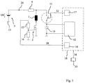
- FIG. 1 A schematic block diagram of an arrangement according to an embodiment of the invention can be seen, an electronic component (measurement object) 1 designed as an inductor being connected in series with a first switch 2 formed by a field effect transistor, thereby forming a first series connection.
- a voltage source 3 is connected to the measurement object 1 with the interposition of an ohmic resistor 4, by means of which an electrical voltage is applied to the first series circuit.
- the voltage source is connected at its one connection to the resistor 4 and at its other connection to ground 13.
- the source connection of the field effect transistor 2 is connected to ground 13.
- a second series circuit is connected in parallel with the first series circuit and has a capacitive memory 10 designed as a capacitor and a second switch 11 connected in series with it.
- the connection of the capacitive memory 10 that is not connected to the switch 11 is connected to ground 13.
- an analog-digital converter 12 is connected in parallel to the capacitive memory 10.
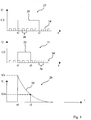
- a first pulse width modulator unit 14 is connected via a voltage divider formed from two resistors 15 and 16 to the gate terminal of the field effect transistor 2, which thus serves as a switch which is switched by means of a switching signal 28 emitted by the pulse width modulator unit 14 (see Fig. 3 ) is opened and / or closed or can be.
- the electronic component 1 can thus be connected to ground 13 or be separated therefrom.
- the switch 2 is formed here by a field effect transistor, the switch 2 can also be formed by another suitable one Be formed component with which an electrical switch can be realized.
- the switch 11 can be switched off by means of a second switching signal 32 (see Fig. 3 ) can be closed and / or opened.
- the two pulse width modulator units 14 and 17 and the digital-to-analog converter 12 are integrated in a microprocessor or microcontroller 18.
- a clock signal 34 is generated by means of a clock generator 33 and is supplied to the microprocessor or microcontroller 18.
- the microprocessor or microcontroller forms a control device, which can alternatively be formed by an FPGA or ASIC.
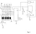
- the switch 11 is formed by means of a multiplexer 19, which is Fig. 2 can be seen.
- the pulse width modulator unit 17 is connected to the enable input E of the multiplexer 19, so that the capacitor 10 is or can be connected in parallel to the electronic component 1 by activating the enable input E (this corresponds to actuating the switch 11).
- the capacitor 10 is separated from the electronic component 1 by deactivating the enable input E by means of the pulse width modulator unit 17 or by means of the second switching signal 32 emitted by it.
- Fig. 2 it can be seen that five additional electronic components (measurement objects) 20 to 24, which are each designed as inductors, are connected at one end to the multiplexer 19 and at the other end to the output of the electronic component 1 connected to the field effect transistor 2. Since the electronic components 1 and 20 to 24 are connected to different connections of the multiplexer 19, the capacitor 10 can be connected to each of these electronic components by means of the multiplexer 19. In this case, the capacitor 10 is always connected to only one or none of the electronic components at a time by means of the multiplexer 19. In order to be able to select which of the electronic components is connected to the capacitor 10 by means of the multiplexer 19, the multiplexer 19 has a plurality of inputs 25, to which suitable signals can be applied or can be applied to select the respective connection. It is thus possible to measure the voltages on the different electronic components 1 and 20 to 24 in succession.
- the multiplexer 19 has a plurality of inputs 25, to which suitable signals can be applied or can be applied to select the respective connection. It is thus possible to measure the voltages
- the resistor 4 with the out Fig. 1 visible node 26 is connected, the other electronic components 20 to 24 with their connections facing away from the switch 2 are each electrically connected to the node 26 via an ohmic resistor 5 to 9.
- the first switching signal 28 emitted by the pulse width modulator unit 14 can be seen in the illustration 27 and rises suddenly to a voltage U1 at a first switching time t1.
- the field effect transistor 2 is turned on or the switch formed by the transistor 2 is closed, so that a voltage is applied to the inductor 1.
- the first switching signal 28 is switched off, which has a blocking effect of the field effect transistor 2. Since the current through a coil is constant, a voltage 30, which can be seen in the illustration 29, is induced in the inductance 1 at the point in time t1, which decays with increasing time t starting from a peak voltage Us.
- the time course of the second switching signal 32 emitted by the pulse width modulator unit 17 can be seen, which likewise rises suddenly to a voltage value U2 at the first switching time t1.
- the switch 11 is closed, so that the voltage applied to the inductance 1 is also applied to the capacitor 10.
- the second switching signal 32 is switched off and the switch 11 is thereby opened, so that the capacitor 10 is separated from the inductance 1.
- the voltage Um applied to the inductance 1 at the time of measurement t3 is held by the capacitor 10 for so long that the analog-digital converter 12 can detect and digitize the voltage Um.
- the digitized voltage Um is then available to the microprocessor 18 for further processing.
- the time difference between t2 and t1 is approximately 2 to 3 ps.
- the inductance is included approx. 10 ⁇ H.
- the processor cycle ⁇ t has a duration of approximately 50 ns, so that the time difference between the first switching point in time t1 and the measuring point in time t3 is or can be set to integer multiples of 50 ns.
- the recurring voltage 30 can be sampled in time increments that correspond to the processor cycle ⁇ t or an integer multiple thereof. How out Fig. 3 can be seen, the courses of the two switching signals 28 and 32 each have a square-wave signal.
Description
Die Erfindung betrifft eine Anordnung zur Messung wenigstens eines Wertes einer an einer elektronischen Komponente anliegenden Spannung. Ferner betrifft die Erfindung ein verfahren zur Abtastung wenigstens eines wertes einer an einer elektronischen Komponente auftretenden Signalflanke.The invention relates to an arrangement for measuring at least one value of a voltage applied to an electronic component. The invention further relates to a method for sampling at least one value of a signal edge occurring on an electronic component.
Die
Die
Die
Die
Aus der
Es gibt verschiedene Verfahren, um Induktivitäts-/Kapazitäts-Werte zu messen. Insbesondere mit Blick auf ein Mikroprozessor-Messsystem für kleine Induktivitäts-/Kapazitäts-Werte und eine gegebenenfalls hohe Anzahl an Messkanälen gibt es eine Reihe von Nachteilen. Zum einen führt die hohe Anzahl analoger Bauelemente zu einem hohen Platzbedarf und zu hohen Kosten. Zum anderen sind derartige Messsysteme anfällig gegenüber Umwelteinflüssen, z.B. gegenüber Temperaturschwankungen. Ferner ist die Realisierung mit einem Mirkoprozessor aufwendig.There are various methods for measuring inductance / capacitance values. In particular with a view to a microprocessor measuring system for small inductance / capacitance values and a possibly high number of measuring channels, there are a number of disadvantages. On the one hand, the large number of analog components leads to a high space requirement and high costs. On the other hand, such measuring systems are susceptible to environmental influences, e.g. against temperature fluctuations. Furthermore, the implementation with a microprocessor is complex.
Ein typisches Messprinzip zur Erfassung von Induktivitäten und Kapazitäten ist es, für die Lade- oder Entladekurve im Strom- oder Spannungsverlauf die Zeit bis zum Erreichen eines Schwellenwertes zu messen. Nachteilig ist dabei, dass die Messung kleiner Induktivitäts- und Kapazitäts-Werte schwierig ist. Ferner ist nachteilig, dass Toleranzen des Schwellenwertschalters das Messergebnis stark beeinflussen. Schließlich ist nachteilig, dass der Messbereich bei kleiner Zeitkonstante durch die Auflösung des Zeit-Zählers eingeschränkt ist.A typical measuring principle for the detection of inductances and capacitances is to measure the time until a threshold value is reached for the charging or discharging curve in the current or voltage curve. The disadvantage here is that the measurement of small inductance and capacitance values is difficult. Another disadvantage is that tolerances of the threshold switch have a strong influence on the measurement result. Finally, it is disadvantageous that the measuring range with a small time constant is limited by the resolution of the time counter.
Ein weiteres Verfahren ist das Abstimmen auf Resonanzfrequenzen, um dadurch die Induktivität oder die Kapazität zu ermitteln. Dieses verfahren ist auch für kleine Induktivitäts-/Kapazitäts-Werte geeignet.Another method is tuning to resonance frequencies in order to determine the inductance or the capacitance. This method is also suitable for small inductance / capacitance values.
Nachteilig ist hierbei, dass zum einen toleranzarme Bauteile erforderlich sind und zum anderen die Dauer der Messung durch die Zeit für den Frequenzdurchlauf (Frequenzsweep) relativ lang ist.The disadvantage here is that, on the one hand, low-tolerance components are required and, on the other hand, the duration of the measurement by the time for the frequency sweep (frequency sweep) is relatively long.
Weist die elektronische Komponente eine relativ kleine Kapazität oder Induktivität auf, so können auftretende Signalflanken, z.B. bei einer Sprungantwort der elektronischen Komponente, sehr steil sein. Zur Messung wenigstens eines Wertes einer solchen schnellen elektrischen Signalflanke ist aber regelmäßig ein schneller Analog-Digital-Wandler erforderlich, der vergleichsweise teuer ist.If the electronic component has a relatively small capacitance or inductance, signal edges which occur, e.g. with a step response of the electronic component, be very steep. To measure at least one value of such a fast electrical signal edge, however, a fast analog-digital converter is regularly required, which is comparatively expensive.
Ausgehend von diesem Stand der Technik liegt der Erfindung die Aufgabe zugrunde, wenigstens einen Wert einer an einer elektronischen Komponente anliegenden Spannung auch bei relativ schnellen Signalflanken mit einer vergleichsweise kostengünstigen und einfach aufgebauten Anordnung messen zu können.Based on this prior art, the object of the invention is to be able to measure at least one value of a voltage applied to an electronic component even with relatively fast signal edges with a comparatively inexpensive and simply constructed arrangement.
Diese Aufgabe wird erfindungsgemäß mit einer Anordnung nach Anspruch 1 und mit einem Verfahren nach Anspruch 11 gelöst. Bevorzugte Weiterbildungen der Erfindung sind in den Unteransprüchen gegeben.This object is achieved with an arrangement according to
Die erfindungsgemäße Anordnung zur Messung wenigstens eines Wertes einer an einer elektronischen Komponente anliegenden Spannung weist einen ersten Signalgeber, von dem ein erstes Schaltsignal abgebbar ist, einen mit dem ersten Signalgeber gekoppelten ersten Schalter, der mittels des ersten Schaltsignals schaltbar ist, wobei die elektronische Komponente mit dem ersten Schalter in Reihe geschaltet und mittels diesem mit einer elektrischen Energiequelle koppelbar ist, einen zweiten Signalgeber, von dem ein zweites Schaltsignal abgebbar ist, einen mit dem zweiten Signalgeber gekoppelten zweiten Schalter, der mittels des zweiten Schaltsignals schaltbar ist, einen kapazitiven Speicher, der mit dem zweiten Schalter in Reihe geschaltet und mittels diesem zu der elektronischen Komponente oder zu der von der elektronischen Komponente und dem ersten Schalter gebildeten Reihenschaltung parallel schaltbar ist, und einen Analog-Digital-Wandler auf, der zu dem kapazitiven Speicher parallel geschaltet ist.The arrangement according to the invention for measuring at least one value of a voltage applied to an electronic component has a first signal generator, from which a first switching signal can be emitted, a first switch coupled to the first signal generator, which can be switched by means of the first switching signal, the electronic component also comprising the first switch is connected in series and can be coupled to an electrical energy source by means of it, a second signal generator, from which a second switching signal can be emitted, a second switch coupled to the second signal generator that can be switched by the second switching signal, a capacitive memory which connected in series with the second switch and can be connected in parallel by means of this to the electronic component or to the series circuit formed by the electronic component and the first switch, and an analog-to-digital converter which is connected in parallel to the capacitive memory is.
Wird der erste Schalter zu einem ersten Zeitpunkt geschlossen, so wird mittels der elektrischen Energiequelle eine elektrische Spannung an die elektronische Komponente angelegt oder ein elektrischer Strom der elektronischen Komponente zugeführt, was bevorzugt zunächst zu einem Ausgleichsvorgang, insbesondere zu einer Sprungantwort, der elektronischen Komponente führt, der nach einer gewissen Zeit in einen stationären oder quasistationären Zustand übergeht. Wird der erste Schalter zu einem späteren, zweiten Schaltzeitpunkt geöffnet, so wird die elektronische Komponente abrupt von der Spannungs- und/oder Stromversorgung getrennt, was bevorzugt ebenfalls zu einem Ausgleichsvorgang, insbesondere zu einer Sprungantwort, der elektronischen Komponente führt. Jeder der Ausgleichsvorgänge hat in der Regel eine Veränderung der an der elektronischen Komponente anliegenden elektrischen Spannung zur Folge, wobei der zeitliche Verlauf der an der elektronischen Komponente anliegenden Spannung während des jeweiligen Ausgleichsvorgangs Rückschlüsse auf elektrische Eigenschaften der elektronischen Komponente zulässt.If the first switch is closed at a first point in time, an electrical voltage is applied to the electronic component is applied or an electrical current is supplied to the electronic component, which preferably initially leads to an equalization process, in particular to a step response, of the electronic component, which changes into a stationary or quasi-stationary state after a certain time. If the first switch is opened at a later, second switching point in time, the electronic component is abruptly disconnected from the voltage and / or power supply, which preferably also leads to a compensation process, in particular to a step response, of the electronic component. Each of the compensation processes generally results in a change in the electrical voltage applied to the electronic component, the course of the voltage applied to the electronic component during the respective compensation process allowing conclusions to be drawn about electrical properties of the electronic component.
Eine an der elektronischen Komponente anliegende Spannung liegt aber im geschlossenen Zustand des zweiten Schalters auch an dem kapazitiven Speicher an. Dabei ist die Kapazität des kapazitiven Speichers bevorzugt derart klein gewählt, dass dieser den Spannungsverlauf an der elektronischen Komponente während eines solchen Ausgleichsvorgangs möglichst wenig oder im Rahmen der gewünschten Messgenauigkeit nicht messbar beeinflusst. Wird nun zu einem Messzeitpunkt der zweite Schalter geöffnet, wird die an dem kapazitiven Speicher anliegende Spannung für eine ausreichende Zeitdauer von dem kapazitiven Speicher gehalten, so dass der Analog-Digital-Wandler diese Spannung erfassen und in ein digitales Signal umwandeln kann.However, a voltage applied to the electronic component is also present in the capacitive memory when the second switch is closed. The capacitance of the capacitive memory is preferably selected to be so small that it influences the voltage profile on the electronic component as little as possible during such an equalization process or not measurably within the desired measurement accuracy. If the second switch is now opened at a time of measurement, the voltage applied to the capacitive memory is held by the capacitive memory for a sufficient period of time so that the analog-digital converter can detect this voltage and convert it into a digital signal.
Ist der zeitliche Unterschied zwischen dem ersten Schaltzeitpunkt und dem Messzeitpunkt und/oder zwischen dem zweiten Schaltzeitpunkt und dem Messzeitpunkt bekannt, ist es möglich, die Spannung an der elektronischen Komponente zu einem bekannten Zeitpunkt nach Beginn des Ausgleichsvorgangs mittels des Analog-Digital-Wandlers zu erfassen und zu digitalisieren. Bevorzugt ist dieser zeitliche Unterschied derart gering, dass der zweite Schalter geöffnet wird, bevor der durch das Schalten des ersten Schalters hervorgerufene Ausgleichsvorgang an der elektronischen Komponente, im Rahmen der Messgenauigkeit, abgeklungen ist.If the time difference between the first switching point and the measuring point and / or between the second switching point and the measuring point is known, it is possible to detect the voltage on the electronic component at a known point in time after the start of the compensation process by means of the analog-digital converter and digitize. This time difference is preferably so small that the second switch is opened before the compensation process on the electronic component caused by the switching of the first switch has subsided, within the scope of the measurement accuracy.
Da kurze zeitliche Unterschiede zwischen zwei Schaltsignalen bei hoher Genauigkeit mit relativ einfachen Mitteln zu erzeugen sind, ist die erfindungsgemäße Anordnung vergleichsweise kostengünstig und einfach im Aufbau realisierbar. Der Analog-Digital-Wandler muss dabei in Bezug auf seine Schnelligkeit nicht dem Ausgleichsvorgang folgen können und kann im Vergleich dazu relativ langsam arbeiten. Bevorzugt sind die Eigenschaften des kapazitiven Speichers aber an die Schnelligkeit des Analog-Digital-Wandlers angepasst, damit der kapazitive Speicher die an ihm anliegende Spannung solange im Rahmen der Messgenauigkeit hält, bis der Analog-Digital-Wandler eine Erfassung und Digitalisierung dieser Spannung durchgeführt hat.Since short time differences between two switching signals can be generated with high accuracy using relatively simple means, the arrangement according to the invention is comparatively inexpensive and simple to implement. The speed of the analog-to-digital converter does not have to be able to follow the compensation process and, in comparison, it can work relatively slowly. However, the properties of the capacitive memory are preferably adapted to the speed of the analog-digital converter, so that the capacitive memory keeps the voltage applied to it within the measurement accuracy until the analog-digital converter has performed a detection and digitization of this voltage ,
Die elektrische Energiequelle, mittels welcher eine elektrische Spannung an die elektronische Komponente angelegt oder ein elektrischer Strom der elektronischen Komponente zugeführt wird oder werden kann, ist bevorzugt eine elektrische Spannungsquelle oder eine elektrische Stromquelle oder weist bevorzugt eine elektrische Spannungsquelle oder eine elektrische Stromquelle auf. Ist der erste Schalter geschlossen, so wird dadurch auch eine Spannung an die elektronische Komponente angelegt und/oder ein. Strom der elektronischen Komponente zugeführt. Die elektrische Energiequelle kann unmittelbar zu der Reihenschaltung aus der elektronischen Komponente und dem ersten Schalter parallel geschaltet sein. Alternativ kann die elektrische Energiequelle unter Zwischenschaltung wenigstens eines zusätzlichen elektronischen Bauelements zu dieser Reihenschaltung parallel geschaltet sein. Das wenigstens eine zusätzliche elektronische Bauelement ist z.B. von einem oder von mehreren ohmschen Widerständen gebildet oder weist diese auf. Insbesondere ist die elektronische Komponente mit der elektrischen Energiequelle unter Zwischenschaltung wenigstens eines ohmschen Widerstands gekoppelt.The electrical energy source, by means of which an electrical voltage is applied to the electronic component or an electrical current can or is supplied to the electronic component, is preferably an electrical voltage source or an electrical current source or preferably has an electrical voltage source or an electrical current source. If the first switch is closed, this also applies a voltage to the electronic component and / or a. Electricity supplied to the electronic component. The electrical energy source can be connected directly in parallel to the series circuit comprising the electronic component and the first switch. Alternatively, the electrical energy source can be connected in parallel with this series connection with the interposition of at least one additional electronic component. The at least one additional electronic component is e.g. formed or has one or more ohmic resistors. In particular, the electronic component is coupled to the electrical energy source with the interposition of at least one ohmic resistor.
Bevorzugt ist der Analog-Digital-Wandler zu dem kapazitiven Speicher direkt parallel geschaltet. Alternativ ist der Analog-Digital-Wandler unter Zwischenschaltung wenigstens eines elektronischen Bauelements parallel zu dem kapazitiven Speicher geschaltet. Dieses wenigstens eine elektronische Bauelement kann z.B. ein ohmscher Widerstand sein.The analog-digital converter is preferably connected directly in parallel to the capacitive memory. Alternatively, the analog-digital converter is connected in parallel with the capacitive memory with the interposition of at least one electronic component. This at least one electronic component can e.g. to be an ohmic resistance.
Der kapazitive Speicher weist bevorzugt wenigstens einen Kondensator auf oder ist von wenigstens einem Kondensator gebildet. Insbesondere kann der kapazitive Speicher auch wenigstens ein anderes elektronisches Bauelement umfassen.The capacitive memory preferably has at least one capacitor or is formed by at least one capacitor. In particular, the capacitive memory also include at least one other electronic component.
Der erste Schalter weist bevorzugt einen Transistor auf oder ist von einem Transistor gebildet, wobei der Transistor insbesondere ein Feldeffekttransistor ist.The first switch preferably has a transistor or is formed by a transistor, the transistor being in particular a field effect transistor.
Der erste Signalgeber weist bevorzugt eine Pulsweitenmodulator-Einheit auf oder ist von einer Pulsweitenmodulator-Einheit gebildet. Mit einer Pulsweitenmodulator-Einheit ist es auf einfache Weise möglich, ein Signal, insbesondere ein Rechtecksignal, zu erzeugen, dessen Impulsdauer und/oder Tastverhältnis mit hoher Genauigkeit einstellbar ist. Ferner weist der zweite Signalgeber bevorzugt eine Pulsweitenmodulator-Einheit auf oder ist von einer Pulsweitenmodulator-Einheit gebildet, sodass auf einfache Weise ein Signal, insbesondere ein Rechtecksignal, mit einstellbarer Impulsdauer und/oder einstellbarem Tastverhältnis erzeugbar ist.The first signal transmitter preferably has a pulse width modulator unit or is formed by a pulse width modulator unit. With a pulse width modulator unit, it is possible in a simple manner to generate a signal, in particular a square-wave signal, whose pulse duration and / or duty cycle can be set with high accuracy. Furthermore, the second signal transmitter preferably has a pulse width modulator unit or is formed by a pulse width modulator unit, so that a signal, in particular a square-wave signal, with an adjustable pulse duration and / or an adjustable pulse duty factor can be generated in a simple manner.
Das erste Schaltsignal ist bevorzugt ein Rechtecksignal oder weist bevorzugt wenigstens ein Rechtecksignal auf. Ferner ist das zweite Schaltsignal bevorzugt ein Rechtecksignal oder weist bevorzugt wenigstens ein Rechtecksignal auf. Insbesondere weist das Rechtecksignal des zweiten Schaltsignals eine unterschiedliche Impulsdauer und/oder ein unterschiedliches Tastverhältnis als das Rechtecksignal des ersten Schaltsignals auf. Bevorzugt weist das Rechtecksignal des zweiten Schaltsignals eine kürzere Impulsdauer und/oder ein kleineres Tastverhältnis als das Rechtecksignal des ersten Schaltsignals auf.The first switching signal is preferably a square-wave signal or preferably has at least one square-wave signal. Furthermore, the second switching signal is preferably a square-wave signal or preferably has at least one square-wave signal. In particular, the square-wave signal of the second switching signal has a different pulse duration and / or a different duty cycle than the square-wave signal of the first switching signal. The square-wave signal of the second switching signal preferably has a shorter pulse duration and / or a smaller duty cycle than the square-wave signal of the first switching signal.
Der zweite Schalter kann ebenfalls von einem Transistor, insbesondere von einem Feldeffekttransistor, gebildet sein. Bevorzugt ist der zweite Schalter von einem Multiplexer gebildet oder mit einem Multiplexer gekoppelt. Insbesondere kann der kapazitive Speicher mittels des Multiplexers zu wenigstens einer anderen elektronischen Komponente, die insbesondere mit dem ersten Schalter in Reihe geschaltet ist, oder zu einer aus der anderen elektronischen Komponente und dem ersten Schalter gebildeten Reihenschaltung parallel geschaltet werden. Vorzugsweise ist die andere elektronische Komponente direkt oder unter Zwischenschaltung wenigstens eines elektronischen Bauelements, wie z.B. eines ohmschen Widerstands, mit der elektrischen Energiequelle gekoppelt oder koppelbar. Mittels des Multiplexeres ist es möglich, Spannungen an unterschiedlichen elektronischen Komponenten zu messen. Die unterschiedlichen elektronischen Komponenten sind dabei bevorzugt an unterschiedlichen Signaleingängen des Multiplexers angeschlossen, die somit unterschiedliche Messkanäle bilden. Der zweite Signalgeber ist insbesondere mit einem Freigabeeingang (enable) des Multiplexers verbunden.The second switch can also be formed by a transistor, in particular by a field effect transistor. The second switch is preferably formed by a multiplexer or coupled to a multiplexer. In particular, the capacitive memory can be connected in parallel with the multiplexer to at least one other electronic component, which is in particular connected in series with the first switch, or to a series circuit formed from the other electronic component and the first switch. The other electronic component is preferably directly or with the interposition of at least one electronic component, such as an ohmic resistor, coupled to the electrical energy source or coupled. Using the multiplexer, it is possible to measure voltages on different electronic components. The different electronic components are preferably connected to different signal inputs of the multiplexer, which thus form different measuring channels. The second signal generator is connected in particular to an enable input of the multiplexer.
Die beiden Signalgeber und/oder der Analog-Digital-Wandler sind bevorzugt in eine Steuereinheit integriert, die insbesondere von einem Mikroprozessor, von einem Mikrokontroller, von einem programmierbaren integrierten Schaltkreis, wie z.B. von einem FPGA, oder von einer anwendungsspezifischen integrierten Schaltung, wie z.B. von einem ASIC, gebildet ist oder diesen bzw. diese umfasst, sodass die erfindungsgemäße Anordnung äußerst platzsparend aufgebaut werden kann. Da Steuereinheiten mit integrierten Analog-Digital-Wandlern und/oder mit integrierten Signalgebern, wie z.B. Pulsweitenmodulator-Einheiten, als Massenprodukt auf dem Markt verfügbar sind, ist die erfindungsgemäße Anordnung äußerst kostengünstig realisierbar. Wie oben bereits angesprochen, ist es dabei nicht nachteilig, wenn der Analog-Digital-Wandler vergleichsweise langsam arbeitet.The two signal transmitters and / or the analog-digital converter are preferably integrated in a control unit, which is in particular operated by a microprocessor, by a microcontroller, by a programmable integrated circuit, such as e.g. from an FPGA, or from an application specific integrated circuit, e.g. is formed by an ASIC, or comprises this or these, so that the arrangement according to the invention can be constructed in an extremely space-saving manner. Since control units with integrated analog-digital converters and / or with integrated signal generators, e.g. Pulse width modulator units, which are available on the market as a mass product, the arrangement according to the invention can be implemented extremely cost-effectively. As already mentioned above, it is not a disadvantage if the analog-digital converter works comparatively slowly.
Weisen die beiden Signalgeber jeweils eine Pulsweitenmodulator-Einheit auf oder sind die beiden Signalgeber jeweils durch eine Pulsweitenmodulator-Einheit gebildet, ist es auf einfache Weise möglich, die Impulsdauern und/oder die Tastverhältnisse der beiden Schaltsignale einzustellen. Somit kann auch der zeitliche Unterschied zwischen dem ersten Schaltzeitpunkt und dem Messzeitpunkt und/oder zwischen dem zweiten Schaltzeitpunkt und dem Messzeitpunkt mit großer Genauigkeit eingestellt werden, insbesondere wenn die beiden Signalgeber zeitlich aufeinander abgestimmt sind, was vorzugsweise auch der Fall ist. Diese zeitliche Abstimmung kann z.B. mittels eines gemeinsamen Taktgebers erfolgen.If the two signal transmitters each have a pulse width modulator unit or if the two signal transmitters are each formed by a pulse width modulator unit, it is possible in a simple manner to set the pulse durations and / or the duty cycle of the two switching signals. The time difference between the first switching time and the measuring time and / or between the second switching time and the measuring time can thus also be set with great accuracy, in particular if the two signal transmitters are time-coordinated, which is preferably also the case. This timing can e.g. by means of a common clock.
Die beiden Signalgeber werden bevorzugt mittels einer gemeinsamen Steuereinrichtung gesteuert oder sind mittels dieser steuerbar, die insbesondere mittels eines Taktgebers getaktet ist, der bevorzugt ein periodisches Taktsignal erzeugt. Somit kann die Impulsdauer und/oder das Tastverhältnis jedes Schaltsignals mit der Genauigkeit eines Taktzyklus oder einem ganzzahligen Vielfachen des Taktzyklus eingestellt werden. Die Impulsdauer jedes Schaltsignals beträgt somit bevorzugt einen oder mehrere Taktzyklen. Ferner unterscheiden sich die Impulsdauern und/oder Impulsenden der beiden Schaltsignale insbesondere um einen Taktzyklus oder um ein ganzzahliges Vielfaches des Taktzyklus. Bevorzugt entspricht der zeitliche Unterschied (Zeitfenster) zwischen dem ersten Schaltzeitpunkt und dem Messzeitpunkt und/oder zwischen dem zweiten Schaltzeitpunkt und dem Messzeitpunkt einem oder einem ganzzahligen Vielfachen des Taktzyklus. Die Steuereinrichtung ist insbesondere von der oben genannten Steuereinheit gebildet, sodass die beiden Signalgeber und/oder der Analog-Digital-Wandler bevorzugt in die getaktete Steuereinrichtung integriert sind.The two signal generators are preferably controlled by means of a common control device or can be controlled by means of this, which is clocked in particular by means of a clock generator, which preferably generates a periodic clock signal. Thus, the pulse duration and / or the duty cycle of each switching signal can be with the accuracy of a clock cycle or an integer multiple of the clock cycle. The pulse duration of each switching signal is therefore preferably one or more clock cycles. Furthermore, the pulse durations and / or pulse ends of the two switching signals differ in particular by one clock cycle or by an integral multiple of the clock cycle. The time difference (time window) between the first switching time and the measuring time and / or between the second switching time and the measuring time preferably corresponds to one or an integer multiple of the clock cycle. The control device is in particular formed by the control unit mentioned above, so that the two signal transmitters and / or the analog-digital converter are preferably integrated in the clocked control device.
Insbesondere geben beide Signalgeber zum ersten Schaltzeitpunkt gleichzeitig ein Schaltsignal ab, welches bevorzugt ein Rechtecksignal ist, sodass beide Schalter gleichzeitig geschlossen werden. Durch Schließen des ersten Schalters wird, wie oben bereits beschrieben, ein Ausgleichsvorgang hervorgerufen, wobei zu dem Messzeitpunkt der kapazitive Speicher von der elektronischen Komponente getrennt wird. Der Unterschied zwischen dem ersten Schaltzeitpunkt und dem nachfolgenden Messzeitpunkt kann einem Taktzyklus oder mehreren Taktzyklen entsprechen. Ein typischer Taktzyklus oder Prozessorzyklus beträgt z.B. 50 ns. Da somit die an der elektronischen Komponente anliegende Spannung zu einem definierten Zeitpunkt nach dem Beginn des Ausgleichsvorgangs mittels des Analog-Digital-Wandler erfasst und digitalisiert werden kann, ist eine Aussage über Eigenschaften der elektronischen Komponente möglich. Um diese Eigenschaften genauer zu bestimmen, kann die Messung mit einem unterschiedlichen zeitlichen Abstand zwischen dem ersten Schaltzeitpunkt und dem Messzeitpunkt wiederholt werden. Somit kann sukzessive eine wiederkehrende Signalflanke abgetastet werden, wobei die zeitliche Auflösung der Abtastung insbesondere dem Taktzyklus oder einem ganzzahligen Vielfachen davon entspricht.In particular, both signal generators emit a switching signal at the first switching instant, which is preferably a square-wave signal, so that both switches are closed simultaneously. As already described above, closing the first switch causes an equalization process, the capacitive memory being separated from the electronic component at the time of measurement. The difference between the first switching time and the subsequent measuring time can correspond to one clock cycle or several clock cycles. A typical clock cycle or processor cycle is e.g. 50 ns. Since the voltage applied to the electronic component can thus be detected and digitized at a defined point in time after the start of the equalization process by means of the analog-digital converter, a statement about the properties of the electronic component is possible. In order to determine these properties more precisely, the measurement can be repeated with a different time interval between the first switching time and the measuring time. A recurring signal edge can thus be sampled successively, the temporal resolution of the sampling corresponding in particular to the clock cycle or an integer multiple thereof.
Gemäß einer Alternative hält das erste Schaltsignal den ersten Schalter solange geschlossen, bis ein möglicher Ausgleichsvorgang abgeklungen und ein stationärer oder quasistationärer Zustand erreicht ist. Wird zum zweiten Schaltzeitpunkt, insbesondere am Ende des ersten Rechtecksignals, der erste Schalter geöffnet, setzt (erneut) ein Ausgleichsvorgang ein. Zum zeitlich hinter dem zweiten Schaltzeitpunkt liegenden Messzeitpunkt wird dann der kapazitive Speicher mittels des zweiten Schalters von der elektronischen Komponente getrennt, sodass die zum Messzeitpunkt an dem kapazitiven Speicher anliegende Spannung, welche der zu diesem Zeitpunkt an der elektronischen Komponente anliegenden Spannung entspricht, mittels des Analog-Digital-Wandlers erfasst und digitalisiert werden kann. Der Messzeitpunkt liegt bevorzugt ein oder mehrere Taktzyklen hinter dem zweiten Schaltzeitpunkt. Da somit die an der elektronischen Komponente anliegende Spannung zu einem definierten Zeitpunkt nach dem Beginn des (erneuten) Ausgleichsvorgangs mittels des Analog-Digital-Wandler erfasst und digitalisiert werden kann, ist eine Aussage über Eigenschaften der elektronischen Komponente möglich. Um diese Eigenschaften genauer zu bestimmen, kann die Messung mit einem unterschiedlichen zeitlichen Abstand zwischen dem zweiten Schaltzeitpunkt und dem Messzeitpunkt wiederholt werden. Somit kann sukzessive eine wiederkehrende Signalflanke abgetastet werden, wobei die zeitliche Auflösung der Abtastung insbesondere dem Prozessorzyklus oder einem ganzzahligen Vielfachen davon entspricht. Vorzugsweise wird auch hier von beiden Signalgebern zum ersten Schaltzeitpunkt gleichzeitig ein Schaltsignal abgegeben, welches insbesondere ein Rechtecksignal ist, wodurch die beiden Schalter gleichzeitig geschlossen werden.According to an alternative, the first switching signal keeps the first switch closed until a possible compensation process has subsided and a stationary or quasi-stationary state has been reached. If the first switch is opened at the second switching point in time, in particular at the end of the first square-wave signal, an equalization process begins (again). At the time of measurement that lies behind the second switching time The capacitive memory is then separated from the electronic component by means of the second switch, so that the voltage present at the capacitive memory at the time of measurement, which corresponds to the voltage present at the electronic component at this time, is detected and digitized by means of the analog-digital converter can. The measurement time is preferably one or more clock cycles after the second switching time. Since the voltage applied to the electronic component can thus be recorded and digitized by means of the analog-digital converter at a defined point in time after the (renewed) equalization process, a statement about the properties of the electronic component is possible. In order to determine these properties more precisely, the measurement can be repeated with a different time interval between the second switching time and the measuring time. A recurring signal edge can thus be sampled successively, the temporal resolution of the sampling corresponding in particular to the processor cycle or an integer multiple thereof. Here, too, preferably a switching signal is emitted by both signal transmitters at the first switching instant, which is in particular a square-wave signal, as a result of which the two switches are closed simultaneously.
Wie oben beschrieben, erzeugt die Steuereinrichtung bevorzugt ein Zeitfenster von 1 bis n Taktzyklen (n ist eine natürliche Zahl), wobei das kleinste Zeitfenster einen Taktzyklus umfasst. Nicht zwingend ist, dass von beiden Signalgebern zum ersten Schaltzeitpunkt gleichzeitig ein Schaltsignal abgegeben wird. Beispielsweise kann der zweite Signalgeber auch zu einem vor oder nach dem ersten Schaltzeitpunkt liegenden Zeitpunkt das zweite Schaltsignal abgeben. Ein Taktzyklus ist bei einem Mikroprozessor oder Mikrocontroller typischerweise ein Prozessorzyklus. Ferner wird das Zeitfenster bevorzugt mittels Pulsweitenmodulation erzeugt. Es ist aber auch möglich, das Zeitfenster mit einem Software-Algorithmus zu erzeugen. Dies geht z.B. bei einem Mikrocontroller mit einem Verfahren ohne Pulsweitenmodulation mit ca. 4 bis n Taktzyklen oder bei einem FPGA ohne Pulsweitenmodulation, indem die Lösung in einer Hardwarebeschreibungssprache, wie z.B. in VHDL, beschrieben wird.As described above, the control device preferably generates a time window of 1 to n clock cycles (n is a natural number), the smallest time window comprising one clock cycle. It is not essential that both signal transmitters emit a switching signal simultaneously at the first switching time. For example, the second signal transmitter can also emit the second switching signal at a point in time before or after the first switching time. A clock cycle in a microprocessor or microcontroller is typically a processor cycle. Furthermore, the time window is preferably generated by means of pulse width modulation. However, it is also possible to generate the time window using a software algorithm. This works e.g. for a microcontroller with a method without pulse width modulation with approx. 4 to n clock cycles or for an FPGA without pulse width modulation, by the solution in a hardware description language, e.g. in VHDL.
Die elektronische Komponente weist wenigstens ein elektronisches Bauelement auf, kann aber auch als elektronische Baugruppe ausgebildet sein. Bevorzugt ist die elektronische Komponente durch wenigstens einen Kondensator oder durch wenigstens eine Induktivität, wie z.B. eine elektrische Spule, gebildet.The electronic component has at least one electronic component, but can also be designed as an electronic assembly. The electronic component is preferred by at least one Capacitor or formed by at least one inductor, such as an electrical coil.
Dem Analog-Digital-Wandler ist bevorzugt eine Auswerteeinrichtung, insbesondere eine digitale Auswerteeinrichtung nachgeschaltet, um z.B. aus dem wenigstens einen gemessenen Wert oder aus den gemessenen Werten eine Eigenschaft der elektronischen Komponente, wie z.B. deren Induktivität oder Kapazität, zu bestimmen. Dabei kann die Auswerteeinrichtung von der Steuereinheit, der Steuereinrichtung, dem Mikroprozessor und/oder Mikrokontroller gebildet sein.An evaluation device, in particular a digital evaluation device, is preferably connected downstream of the analog-digital converter in order, for example, to from the at least one measured value or from the measured values a property of the electronic component, such as to determine their inductance or capacitance. The evaluation device can be formed by the control unit, the control device, the microprocessor and / or microcontroller.
Die Erfindung betrifft ferner die Verwendung der erfindungsgemäßen Anordnung zur Bestimmung einer Eigenschaft, vorzugsweise einer elektrischen Eigenschaft, insbesondere der Induktivität oder der Kapazität, der wenigstens einen elektronischen Komponente.The invention further relates to the use of the arrangement according to the invention for determining a property, preferably an electrical property, in particular the inductance or the capacitance, of the at least one electronic component.
Zusätzlich betrifft die Erfindung ein Verfahren zur Abtastung wenigstens eines Wertes einer an einer elektronischen Komponente auftretenden Signalflanke, wobei
- a) zu einem ersten Schaltzeitpunkt an die elektronische Komponente eine Spannung angelegt und/oder der elektronischen Komponente ein Strom zugeführt wird,
- b) ein kapazitiver Speicher zu der elektronischen Komponente parallel geschaltet wird,
- c) zu einem Messzeitpunkt der kapazitive Speicher von der elektronischen Komponente getrennt wird, wobei der Messzeitpunkt um eine Zeitdifferenz zeitlich hinter dem ersten Schaltzeitpunkt liegt,
- d) die zum Messzeitpunkt an dem kapazitiven Speicher anliegende Spannung erfasst und digitalisiert wird.
- a) a voltage is applied to the electronic component and / or a current is supplied to the electronic component at a first switching time,
- b) a capacitive memory is connected in parallel to the electronic component,
- c) the capacitive memory is separated from the electronic component at a measurement time, the measurement time being a time difference behind the first switching time,
- d) the voltage applied to the capacitive memory at the time of measurement is recorded and digitized.
Dabei wird der Verfahrensschritt b) insbesondere zum ersten Schaltzeitpunkt durchgeführt. Ferner werden die Verfahrensschritte a) bis d) bevorzugt bei einer unterschiedlichen Zeitdifferenz wenigstens einmal wiederholt. Auch kann die elektronische Komponente wenigstens einmal durch eine andere elektronische Komponente ausgetauscht werden, wonach oder wobei nach jedem Austausch die Verfahrensschritte a) bis d) wiederholt werden.Method step b) is carried out in particular at the first switching time. Furthermore, the method steps a) to d) are preferably repeated at least once with a different time difference. The electronic component can also be replaced at least once by another electronic component, after which or after each exchange, the process steps a) to d) are repeated.
Zum Durchführen des Verfahrens wird insbesondere die erfindungsgemäße Anordnung verwendet, so dass die für das Verfahren verwendeten elektronischen Bauelemente den elektronischen Bauelementen der Anordnung entsprechen können und wie beschrieben weitergebildet sein können. Insbesondere kann ein periodisches Taktsignal erzeugt werden, wobei der Unterschied zwischen dem ersten Schaltzeitpunkt und dem Messzeitpunkt bevorzugt einem oder einem ganzzahligen Vielfachen des Taktzyklus des Taktsignals entspricht.The arrangement according to the invention is used in particular to carry out the method, so that the electronic components used for the method can correspond to the electronic components of the arrangement and can be further developed as described. In particular, a periodic clock signal can be generated, the difference between the first switching instant and the measuring instant preferably corresponding to one or an integer multiple of the clock cycle of the clock signal.
Ziel der Erfindung ist insbesondere die Abtastung schneller elektrischer Signalflanken und die Bewertung des Verlaufs, z.B. zur Messung von Induktivitäten oder Kapazitäten. Vorteilhaft ist hier der geringe technische und kostenmäßige Aufwand, um eine hohe Anzahl an Messkanälen zu erfassen, an denen jeweils nur kleine Kapazitäten oder Induktivitäten, von z.B. 1 µH, vorhanden sind.The aim of the invention is in particular the scanning of fast electrical signal edges and the evaluation of the course, e.g. for measuring inductance or capacitance. The advantage here is the low technical and costly effort to acquire a large number of measuring channels, on each of which only small capacities or inductors, e.g. 1 µH are present.
Bei der Ansteuerung einer kapazitiv oder induktiv wirkenden elektronischen Komponente kommt es nach Anlegen eines Rechtecksignals zu einem zeitlichen verzögerten Spannungsverlauf, der von der Induktivität und/oder Kapazität und/oder vom ohmschen Widerstand der elektronischen Komponente abhängig ist. Diese zeitlichen Abläufe sind bei einer geringen Induktivität oder bei einer geringen Kapazität so schnell, dass eine Abtastung des Signalverlaufs mit einfachen, kostengünstigen Analog-Digital-Wandlern nicht möglich ist, da keine ausreichende Abtastrate erreicht wird.When a capacitive or inductive electronic component is activated, a time-delayed voltage curve occurs after the application of a square wave signal, which is dependent on the inductance and / or capacitance and / or on the ohmic resistance of the electronic component. With a low inductance or a small capacitance, these time sequences are so fast that it is not possible to sample the signal curve with simple, inexpensive analog-digital converters, since an adequate sampling rate is not achieved.
Der erfindungsgemäßen Lösung liegt bevorzugt zugrunde, dass ein Mikroprozessor mit einer Pulsweitenmodulator-Einheit selbst ein Rechtecksignal zum Messobjekt (elektronische Komponente) schickt. Synchron dazu wird eine zweite Pulsweitenmodulator-Einheit gestartet. Der Rechteckimpuls der ersten Pulsweitenmodulator-Einheit erregt das Messobjekt oder mehrere Messobjekte. Die zweite Pulsweitenmodulator-Einheit unterbricht das zurückgeführte Signal vom Messobjekt zum Analog-Digital-Wandler des Mikrokontrollers mit einem Versatz von 1 bis n Prozessorzyklen (n steht für ein natürliche Zahl) und speichert dadurch den analogen Spannungswert in einem Kondensator (Abtast-Halte-Prinzip oder Sample and Hold Prinzip). Der Prozessorzyklus bestimmt dabei die Auflösung der Pulsweitenmodulator-Einheit. Ein langsamer Analog-Digital-Wandler (extern oder im Mikroprozessor integriert) kann damit das gespeicherte Signal abtasten. Durch das repetierende Signal der ersten Pulsweitenmodulator-Einheit und dem Jitter (Schwanken) von 1 bis n Prozessorzyklen der Impulsdauer des zweiten Pulsweitenmodulator-Signals relativ zu der Impulsdauer des ersten Pulsweitenmodulator-Signals kann in mehreren Zyklen die schnelle Impulsantwort des Messobjekts mit 1 bis n Abtastungen zeitlich diskretisiert und ausgewertet werden.The solution according to the invention is preferably based on the fact that a microprocessor with a pulse width modulator unit itself sends a square-wave signal to the measurement object (electronic component). A second pulse width modulator unit is started synchronously. The rectangular pulse of the first pulse width modulator unit excites the measurement object or several measurement objects. The second pulse width modulator unit interrupts the returned signal from the test object to the analog-to-digital converter of the microcontroller with an offset of 1 to n processor cycles (n stands for a natural number) and thereby stores the analog voltage value in a capacitor (sample-hold principle or sample and hold principle). The processor cycle determines the resolution of the pulse width modulator unit. A slow analog-digital converter (external or integrated in the microprocessor) can do that Scan the stored signal. Due to the repetitive signal of the first pulse width modulator unit and the jitter (fluctuation) from 1 to n processor cycles of the pulse duration of the second pulse width modulator signal relative to the pulse duration of the first pulse width modulator signal, the rapid impulse response of the measurement object can be carried out with 1 to n samples in several cycles time discretized and evaluated.
Die zweite Pulsweitenmodulator-Einheit schaltet dabei bevorzugt direkt das Freigabesignal eines Signalmultiplexers. Der Multiplexer dient damit zur Messkanalumschaltung, wie auch zur Steuerung der Abtast-HalteFunktion.The second pulse width modulator unit preferably switches the enable signal of a signal multiplexer directly. The multiplexer is used for measuring channel switching as well as for controlling the sample and hold function.
Ein bevorzugtes Merkmal der Erfindung ist das Zeitverhalten, d.h. dass Schaltsignale in einem Zeitfenster mit 1 bis n Taktzyklen zyklusgenau gesteuert werden können, wobei ein Zyklus insbesondere der schnellsten Befehlsausführungszeit oder der Taktgeschwindigkeit der Steuereinrichtung entspricht. Bevorzugt synchronisiert die Steuereinrichtung das gesamte Zeitverhalten auf die Wandlerzeiten des Analog-Digital-Wandlers. Somit ist es möglich, einen im Mikrocontroller integrierten oder einen externen Analog-Digital-Wandler zu verwenden, der im Vergleich zu den interessierenden zeitlichen Abläufen relativ langsam arbeitet.A preferred feature of the invention is the timing, i.e. that switching signals can be controlled cycle-precisely in a time window with 1 to n clock cycles, a cycle corresponding in particular to the fastest command execution time or the clock speed of the control device. The control device preferably synchronizes the entire time behavior to the converter times of the analog-digital converter. It is thus possible to use an analog-digital converter integrated in the microcontroller or an external one, which works relatively slowly in comparison to the temporal processes of interest.
Die Erfindung bietet insbesondere folgende Vorteile:
- Hohe Abtastraten sind mit einem Mikroprozessor möglich. Insbesondere ist eine bis zu hundertfach höhere analoge Abtastrate möglich als dies für einen typischen Mikroprozessor mit Analog-Digital-Wandler spezifiziert ist.
- Es ist eine einfache Signalkonditionierung für eine hohe Anzahl von Sensorkanälen möglich.
- Es ist keine analoge Aufbereitung erforderlich; es ist ein rein digitales System bis zum Analog-Digital-Wandler möglich; es sind einfache Multiplexer verwendbar.
- Es ist eine Reduzierung der Bauteilanzahl möglich.
- Es wird lediglich ein geringer Bauraum benötigt.
- Es ist eine Kostenreduzierung möglich.
- Die Anordnung und/oder das Verfahren sind weitgehend temperaturstabil, unter anderem durch eine geringe Anzahl von Halbleitern und geringe analoge Schaltungsanteile.
- High sampling rates are possible with a microprocessor. In particular, an analog sampling rate that is up to a hundred times higher than is specified for a typical microprocessor with an analog-digital converter is possible.
- Simple signal conditioning for a large number of sensor channels is possible.
- No analog preparation is required; a purely digital system up to the analog-digital converter is possible; simple multiplexers can be used.
- The number of components can be reduced.
- Only a small space is required.
- A cost reduction is possible.
- The arrangement and / or the method are largely temperature-stable, inter alia due to a small number of semiconductors and small analog circuit components.
Die Erfindung wird nachfolgend anhand einer bevorzugten Ausführungsform unter Bezugnahme auf die Zeichnung beschrieben. In der Zeichnung zeigen:
- Fig. 1
- ein schematisches Blockschaltbild einer Anordnung gemäß einer Ausführungsform der Erfindung,
- Fig. 2
- ein teilweises Blockschaltbilds der Anordnung mit mehreren Messobjekten und
- Fig. 3
- eine schematische Darstellung von Signalverläufen gemäß der Ausführungsform.
- Fig. 1
- 2 shows a schematic block diagram of an arrangement according to an embodiment of the invention,
- Fig. 2
- a partial block diagram of the arrangement with several objects and
- Fig. 3
- a schematic representation of waveforms according to the embodiment.
Aus
Eine erste Pulsweitenmodulator-Einheit 14 ist über einen aus zwei Widerständen 15 und 16 gebildeten Spannungsteiler mit dem Gate-Anschluss des Feldeffekttransistors 2 verbunden, welcher somit als Schalter dient, der mittels eines von der Pulsweitenmodulator-Einheit 14 abgegebenen Schaltsignals 28 (siehe
Der Schalter 11 ist mittels eines Multiplexers 19 gebildet, was aus
Aus
Wie die elektronische Komponente 1, die über den Widerstand 4 mit dem aus
Aus
Bei einer beispielhaften Ausgestaltung liegt die zeitliche Differenz zwischen t2 und t1 bei ca. 2 bis 3 ps. Die Induktivität liegt bei ca. 10 µH. Ferner hat der Prozessorzyklus Δt eine Dauer von etwa 50 ns, sodass der zeitliche Unterschied zwischen dem ersten Schaltzeitpunkt t1 und dem Messzeitpunkt t3 auf ganzzahlige Vielfache von 50 ns eingestellt ist oder werden kann. Durch Wiederholen der Messung bei unterschiedlichen zeitlichen Differenzen zwischen dem Messzeitpunkt t3 und dem ersten Schaltzeitpunkt t1 kann die wiederkehrende Spannung 30 in zeitlichen Schritten abgetastet werden, die dem Prozessorzyklus Δt oder einem ganzzahligen Vielfachen davon entsprechen. Wie aus
- 11
- Induktivitätinductance
- 22
- Schalter / FeldeffekttransistorSwitch / field effect transistor
- 33
- Spannungsquellevoltage source
- 44
- Widerstandresistance
- 55
- Widerstandresistance
- 66
- Widerstandresistance
- 77
- Widerstandresistance
- 88th
- Widerstandresistance
- 99
- Widerstandresistance
- 1010
- Kondensatorcapacitor
- 1111
- Schalterswitch
- 1212
- Analog-Digital-WandlerAnalog to digital converter
- 1313
- MasseDimensions
- 1414
- Pulsweitenmodulator-EinheitPulse width modulator unit
- 1515
- Widerstandresistance
- 1616
- Widerstandresistance
- 1717
- Pulsweitenmodulator-EinheitPulse width modulator unit
- 1818
- Mikroprozessormicroprocessor
- 1919
- Multiplexermultiplexer
- 2020
- Induktivitätinductance
- 2121
- Induktivitätinductance
- 2222
- Induktivitätinductance
- 2323
- Induktivitätinductance
- 2424
- Induktivitätinductance
- 2525
- Eingängeinputs
- 2626
- Knotennode
- 2727
- Darstellungpresentation
- 2828
- erstes Schaltsignalfirst switching signal
- 2929
- Darstellungpresentation
- 3030
- Spannung an InduktivitätVoltage at inductance
- 3131
- Darstellungpresentation
- 3232
- zweites Schaltsignalsecond switching signal
- 3333
- Taktgeberclock
- 3434
- Taktsignalclock signal
- UU
- Spannungtension
- U0U0
- Spannung der SpannungsquelleVoltage of the voltage source
- U1U1
- Schaltspannung des ersten SchaltsignalsSwitching voltage of the first switching signal
- U2U2
- Schaltspannung des zweiten SchaltsignalsSwitching voltage of the second switching signal
- UsUs
- Spitzenspannung an InduktivitätPeak voltage on inductance
- UmAround
- Messspannungmeasuring voltage
- Ee
- Freigabeeingang des MultiplexersRelease input of the multiplexer
- tt
- Zeittime
- t1t1
- erster Schaltzeitpunktfirst switching time
- t2t2
- zweiter Schaltzeitpunktsecond switching time
- t3t3
- MesszeitpunktMeasuring time
- Δt.delta.t
- Taktzyklus des TaktsignalsClock cycle of the clock signal
Claims (14)
- Arrangement for measuring at least one value of a voltage applied to an electronic component (1), having the electronic component (1),
a first signal transmitter (14), from which a first switching signal (28) is able to be output,
a first switch (2), which is coupled to the first signal transmitter (14) and which is able to be switched by means of the first switching signal (28), wherein the electronic component (1) is connected in series with the first switch (2) and is able to be coupled by means of said first switch to an electrical energy source (3) at a first switching time (t1),
a second signal transmitter (17), from which a second switching signal (32) is able to be output,
and
an analogue-to-digital converter (12),
characterized by
a second switch (11), which is coupled to the second signal transmitter (17), is formed from a transistor and is able to be switched by means of the second switching signal (32),
and
a capacitive store (10), which is connected in series with the second switch (11) and by means of said second switch is connected directly in parallel with the series circuit formed by the electronic component (1) and the first switch (2) and is disconnected at a measurement time (t3) that lies in terms of time behind the first switching time (t1) by a time difference,
wherein the analogue-to-digital converter (12) is connected in parallel with the capacitive store (10). - Arrangement according to Claim 1,
characterized in that
the electronic component (1) is coupled or is able to be coupled to the electrical energy source (3) with the interconnection of at least one ohmic resistor (4). - Arrangement according to Claim 1 or 2,
characterized in that
the capacitive store has a capacitor (10) or is formed thereby. - Arrangement according to one of the preceding claims,
characterized in that
the first switch has a transistor (2) or is formed thereby. - Arrangement according to one of the preceding claims,
characterized in that
the first signal transmitter has a pulse-width-modulator unit (14) or is formed thereby, wherein the first switching signal (28) is or has a square-wave signal. - Arrangement according to Claim 5,
characterized in that
the second signal transmitter has a pulse-width-modulator unit (17) or is formed thereby, wherein the second switching signal (32) is or has a square-wave signal, the pulse duration of which is shorter than the pulse duration of the square-wave signal of the first switching signal (28). - Arrangement according to one of the preceding claims,
characterized in that
the second switch is formed by a multiplexer (19) or is coupled to a multiplexer, wherein the capacitive store (10) is able to be connected in parallel by means of the multiplexer (19) with at least one other electronic component (20) connected in series with the first switch (2) or with a series circuit formed from the other electronic component (20) and the first switch (2). - Arrangement according to one of the preceding claims,
characterized in that
the two signal transmitters (14, 17) and the analogue-to-digital converter (12) are integrated in a microprocessor or microcontroller (18). - Arrangement according to one of the preceding claims,
characterized in that
the two signal transmitters (14, 17) and the analogue-to-digital converter (12) are integrated in a clocked control device (18), wherein the pulse ends of the two switching signals (28, 32) differ by one clock cycle or an integer multiple of the clock cycle of the control device (18). - Use of the arrangement according to one of the preceding claims to determine the inductance or the capacitance of the electronic component (1).
- Method for sampling at least one value of a signal edge arising at an electronic component (1) by means of an arrangement according to one of the preceding claims, whereina) a voltage is applied to the electronic component (1) and/or a current is supplied to the electronic component (1) at a first switching time (t1),b) the series circuit formed from the capacitive store (10) and the second switch (11) is connected directly in parallel with the series circuit formed from the electronic component (1) and the first switch (2),c) the capacitive store (10) is disconnected from the electronic component (1) at a measurement time (t3), wherein the measurement time (t3) lies in terms of time behind the first switching time (t1) by a time difference,d) the voltage applied to the capacitive store (10) at the measurement time (t3) is detected and digitized.
- Method according to Claim 11,
characterized in that
method step b) is carried out at the first switching time (t1) . - Method according to Claim 11 or 12,
characterized in that
method steps a) to d) are repeated in the case of a different time difference. - Method according to one of Claims 11 to 13,
characterized in that
a periodic clock signal (34) is generated, wherein the time difference corresponds to one clock cycle or an integer multiple of the clock cycle (Δt) of the clock signal (34).
Applications Claiming Priority (2)
| Application Number | Priority Date | Filing Date | Title |
|---|---|---|---|
| DE102008044908A DE102008044908A1 (en) | 2008-08-29 | 2008-08-29 | Arrangement for measuring at least one value of a voltage applied to an electronic component voltage |
| PCT/DE2009/001121 WO2010022700A2 (en) | 2008-08-29 | 2009-08-12 | Arrangement for measuring at least one value of a voltage applied to an electronic component |
Publications (2)
| Publication Number | Publication Date |
|---|---|
| EP2318850A2 EP2318850A2 (en) | 2011-05-11 |
| EP2318850B1 true EP2318850B1 (en) | 2020-01-01 |
Family
ID=41605996
Family Applications (1)
| Application Number | Title | Priority Date | Filing Date |
|---|---|---|---|
| EP09744592.8A Active EP2318850B1 (en) | 2008-08-29 | 2009-08-12 | Arrangement for measuring at least one value of a voltage applied to an electronic component |
Country Status (7)
| Country | Link |
|---|---|
| US (1) | US8508215B2 (en) |
| EP (1) | EP2318850B1 (en) |
| JP (1) | JP5492892B2 (en) |
| CN (1) | CN102138078B (en) |
| DE (1) | DE102008044908A1 (en) |
| ES (1) | ES2770644T3 (en) |
| WO (1) | WO2010022700A2 (en) |
Families Citing this family (5)
| Publication number | Priority date | Publication date | Assignee | Title |
|---|---|---|---|---|
| CN102445590A (en) * | 2011-12-21 | 2012-05-09 | 上海博泰悦臻电子设备制造有限公司 | Current detection circuit used for judging state of an antenna |
| DE102016002896A1 (en) * | 2016-03-09 | 2017-09-14 | Diehl Ako Stiftung & Co. Kg | Control device and method for detecting an operation by a user of controls incorporated in sensor circuits |
| CN109863410B (en) * | 2017-09-19 | 2021-03-05 | 深圳市汇顶科技股份有限公司 | Method and system for measuring power-on reset time |
| JP7456831B2 (en) | 2019-04-17 | 2024-03-27 | メトラー-トレド・セーフライン・リミテッド | Methods for operating metal detectors and metal detectors |
| EP3726255A1 (en) * | 2019-04-17 | 2020-10-21 | Mettler-Toledo Safeline Limited | Method for operating a metal detector and metal detector |
Family Cites Families (13)
| Publication number | Priority date | Publication date | Assignee | Title |
|---|---|---|---|---|
| JPS5411712B2 (en) * | 1972-05-17 | 1979-05-17 | ||
| EP0126846B1 (en) * | 1983-04-21 | 1990-08-01 | WABCO Westinghouse Fahrzeugbremsen GmbH | Inductive sensor |
| DE3343885C2 (en) * | 1983-04-21 | 1996-12-12 | Wabco Gmbh | Inductive sensor |
| FR2564205B1 (en) * | 1984-05-10 | 1986-10-24 | Univ Rennes | METHOD AND DEVICE FOR THE QUICK TEST OF CAPACITORS AND DIELECTRIC MATERIALS |
| DE3421873A1 (en) * | 1984-06-13 | 1985-12-19 | Brown, Boveri & Cie Ag, 6800 Mannheim | MEASURING METHOD FOR DETERMINING THE DIFFERENCE BETWEEN AN AC VOLTAGE AND A SECOND VOLTAGE, AND MEASURING DEVICE FOR ITS APPLICATION |
| EP0288215B1 (en) * | 1987-04-24 | 1993-03-10 | Simmonds Precision Products Inc. | Determination of electrical capacitance and resistance |
| EP0438103A3 (en) * | 1990-01-15 | 1992-05-06 | Dieter Dr. Weiss | Process and appliance for measuring physical sizes |
| US5469364A (en) * | 1993-03-15 | 1995-11-21 | Hughey; Bradley W. | Apparatus and methods for measuring and detecting variations in the value of a capacitor |
| DE10118299B4 (en) * | 2001-04-12 | 2005-02-10 | Conti Temic Microelectronic Gmbh | Method for determining the ohmic component of the internal resistance of a capacitor and apparatus for carrying out the method |
| JP2003254998A (en) * | 2002-03-04 | 2003-09-10 | Yazaki Corp | Cell voltage measuring method of battery pack and its device |
| KR100845320B1 (en) * | 2006-07-24 | 2008-07-10 | 주식회사 애트랩 | Apparatus using battery and method of detecting exchange or recharge time of battery thereof |
| KR100915825B1 (en) * | 2008-02-13 | 2009-09-07 | 주식회사 하이닉스반도체 | Circuit for Detecting Pumping Voltage of Semiconductor Memory Apparatus |
| US8054090B2 (en) * | 2008-10-22 | 2011-11-08 | Atmel Corporation | Noise handling in capacitive touch sensors |
-
2008
- 2008-08-29 DE DE102008044908A patent/DE102008044908A1/en not_active Ceased
-
2009
- 2009-08-12 US US13/060,876 patent/US8508215B2/en active Active
- 2009-08-12 ES ES09744592T patent/ES2770644T3/en active Active
- 2009-08-12 EP EP09744592.8A patent/EP2318850B1/en active Active
- 2009-08-12 WO PCT/DE2009/001121 patent/WO2010022700A2/en active Application Filing
- 2009-08-12 JP JP2011524177A patent/JP5492892B2/en active Active
- 2009-08-12 CN CN200980134044.0A patent/CN102138078B/en active Active
Non-Patent Citations (1)
| Title |
|---|
| None * |
Also Published As
| Publication number | Publication date |
|---|---|
| CN102138078B (en) | 2015-08-19 |
| JP5492892B2 (en) | 2014-05-14 |
| JP2012500978A (en) | 2012-01-12 |
| CN102138078A (en) | 2011-07-27 |
| DE102008044908A1 (en) | 2010-03-04 |
| US20110163734A1 (en) | 2011-07-07 |
| EP2318850A2 (en) | 2011-05-11 |
| US8508215B2 (en) | 2013-08-13 |
| WO2010022700A3 (en) | 2010-05-14 |
| ES2770644T3 (en) | 2020-07-02 |
| WO2010022700A2 (en) | 2010-03-04 |
Similar Documents
| Publication | Publication Date | Title |
|---|---|---|
| DE69920034T3 (en) | Charge transfer capacitance measurement circuit | |
| DE102013105415B4 (en) | Method and apparatus for sampling an input signal | |
| EP2318850B1 (en) | Arrangement for measuring at least one value of a voltage applied to an electronic component | |
| WO2012004028A1 (en) | Detecting a dielectric article | |
| DE19701262A1 (en) | Passing magnetic article detector with automatic gain control | |
| WO2003071233A1 (en) | Device and method for reading out a differential capacitor comprising a first and second partial capacitor | |
| WO2007122123A2 (en) | Method and circuit arrangement for measuring a capacitance | |
| DE3690624C2 (en) | ||
| DE102010049488B4 (en) | Method for testing a laboratory device and appropriately equipped laboratory device | |
| WO2016041726A1 (en) | Device and method for monitoring a process variable of a medium | |
| DE19631972C2 (en) | Method for monitoring the functionality of an analog / digital converter designed for digitizing analog signals | |
| DE4306950C2 (en) | Electronic two-wire switching device | |
| DE19703633C2 (en) | Method for determining a time interval between two events | |
| EP1769289A1 (en) | Method and device for the highly accurate digital measurement of an analogue signal | |
| EP1093224A2 (en) | Pulse detector and method for the detection of sinusoidal pulses | |
| DE2743410B2 (en) | Method for the temporal stabilization of periodic sampling pulses and arrangements for carrying out the method | |
| DE102013005178B4 (en) | Impedance scanner | |
| DE2547746A1 (en) | DEVICE WITH A SENSOR UNIT FOR GENERATING A SEQUENCE OF VOLTAGE VALUES AND AN AVERATING UNIT | |
| WO2006122768A1 (en) | Circuit arrangement for a capacitive proximity switch | |
| EP3345006B1 (en) | Apparatus for recording a resistance value of a measuring resistor of a measuring sensor | |
| WO2023160950A1 (en) | Method and circuit arrangement for determining an inductance of a measuring coil | |
| EP2330478A1 (en) | Switch and method for determining a value, in particular duration of a measurement signal | |
| DE2335832C3 (en) | Methods and devices for parameter measurement of LC resonance circuit elements | |
| DE1489129B1 (en) | Time deflection voltage generator for a cathode ray tube | |
| DE2343550C3 (en) | Method and device for measuring parameters of the components of a complex circuit |
Legal Events
| Date | Code | Title | Description |
|---|---|---|---|
| PUAI | Public reference made under article 153(3) epc to a published international application that has entered the european phase |
Free format text: ORIGINAL CODE: 0009012 |
|
| 17P | Request for examination filed |
Effective date: 20110209 |
|
| AK | Designated contracting states |
Kind code of ref document: A2 Designated state(s): AT BE BG CH CY CZ DE DK EE ES FI FR GB GR HR HU IE IS IT LI LT LU LV MC MK MT NL NO PL PT RO SE SI SK SM TR |
|
| AX | Request for extension of the european patent |
Extension state: AL BA RS |
|
| DAX | Request for extension of the european patent (deleted) | ||
| 17Q | First examination report despatched |
Effective date: 20130109 |
|
| GRAP | Despatch of communication of intention to grant a patent |
Free format text: ORIGINAL CODE: EPIDOSNIGR1 |
|
| STAA | Information on the status of an ep patent application or granted ep patent |
Free format text: STATUS: GRANT OF PATENT IS INTENDED |
|
| INTG | Intention to grant announced |
Effective date: 20190719 |
|
| GRAS | Grant fee paid |
Free format text: ORIGINAL CODE: EPIDOSNIGR3 |
|
| GRAA | (expected) grant |
Free format text: ORIGINAL CODE: 0009210 |
|
| STAA | Information on the status of an ep patent application or granted ep patent |
Free format text: STATUS: THE PATENT HAS BEEN GRANTED |
|
| AK | Designated contracting states |
Kind code of ref document: B1 Designated state(s): AT BE BG CH CY CZ DE DK EE ES FI FR GB GR HR HU IE IS IT LI LT LU LV MC MK MT NL NO PL PT RO SE SI SK SM TR |
|
| REG | Reference to a national code |
Ref country code: GB Ref legal event code: FG4D Free format text: NOT ENGLISH |
|
| REG | Reference to a national code |
Ref country code: AT Ref legal event code: REF Ref document number: 1220449 Country of ref document: AT Kind code of ref document: T Effective date: 20200115 Ref country code: CH Ref legal event code: EP |
|
| REG | Reference to a national code |
Ref country code: IE Ref legal event code: FG4D Free format text: LANGUAGE OF EP DOCUMENT: GERMAN |
|
| REG | Reference to a national code |
Ref country code: DE Ref legal event code: R096 Ref document number: 502009016076 Country of ref document: DE |
|
| REG | Reference to a national code |
Ref country code: NL Ref legal event code: MP Effective date: 20200101 |
|
| REG | Reference to a national code |
Ref country code: ES Ref legal event code: FG2A Ref document number: 2770644 Country of ref document: ES Kind code of ref document: T3 Effective date: 20200702 |
|
| REG | Reference to a national code |
Ref country code: LT Ref legal event code: MG4D |
|
| PG25 | Lapsed in a contracting state [announced via postgrant information from national office to epo] |
Ref country code: NO Free format text: LAPSE BECAUSE OF FAILURE TO SUBMIT A TRANSLATION OF THE DESCRIPTION OR TO PAY THE FEE WITHIN THE PRESCRIBED TIME-LIMIT Effective date: 20200401 Ref country code: FI Free format text: LAPSE BECAUSE OF FAILURE TO SUBMIT A TRANSLATION OF THE DESCRIPTION OR TO PAY THE FEE WITHIN THE PRESCRIBED TIME-LIMIT Effective date: 20200101 Ref country code: LT Free format text: LAPSE BECAUSE OF FAILURE TO SUBMIT A TRANSLATION OF THE DESCRIPTION OR TO PAY THE FEE WITHIN THE PRESCRIBED TIME-LIMIT Effective date: 20200101 Ref country code: PT Free format text: LAPSE BECAUSE OF FAILURE TO SUBMIT A TRANSLATION OF THE DESCRIPTION OR TO PAY THE FEE WITHIN THE PRESCRIBED TIME-LIMIT Effective date: 20200527 Ref country code: NL Free format text: LAPSE BECAUSE OF FAILURE TO SUBMIT A TRANSLATION OF THE DESCRIPTION OR TO PAY THE FEE WITHIN THE PRESCRIBED TIME-LIMIT Effective date: 20200101 Ref country code: CZ Free format text: LAPSE BECAUSE OF FAILURE TO SUBMIT A TRANSLATION OF THE DESCRIPTION OR TO PAY THE FEE WITHIN THE PRESCRIBED TIME-LIMIT Effective date: 20200101 |
|
| PG25 | Lapsed in a contracting state [announced via postgrant information from national office to epo] |
Ref country code: BG Free format text: LAPSE BECAUSE OF FAILURE TO SUBMIT A TRANSLATION OF THE DESCRIPTION OR TO PAY THE FEE WITHIN THE PRESCRIBED TIME-LIMIT Effective date: 20200401 Ref country code: SE Free format text: LAPSE BECAUSE OF FAILURE TO SUBMIT A TRANSLATION OF THE DESCRIPTION OR TO PAY THE FEE WITHIN THE PRESCRIBED TIME-LIMIT Effective date: 20200101 Ref country code: GR Free format text: LAPSE BECAUSE OF FAILURE TO SUBMIT A TRANSLATION OF THE DESCRIPTION OR TO PAY THE FEE WITHIN THE PRESCRIBED TIME-LIMIT Effective date: 20200402 Ref country code: HR Free format text: LAPSE BECAUSE OF FAILURE TO SUBMIT A TRANSLATION OF THE DESCRIPTION OR TO PAY THE FEE WITHIN THE PRESCRIBED TIME-LIMIT Effective date: 20200101 Ref country code: LV Free format text: LAPSE BECAUSE OF FAILURE TO SUBMIT A TRANSLATION OF THE DESCRIPTION OR TO PAY THE FEE WITHIN THE PRESCRIBED TIME-LIMIT Effective date: 20200101 Ref country code: IS Free format text: LAPSE BECAUSE OF FAILURE TO SUBMIT A TRANSLATION OF THE DESCRIPTION OR TO PAY THE FEE WITHIN THE PRESCRIBED TIME-LIMIT Effective date: 20200501 |
|
| REG | Reference to a national code |
Ref country code: DE Ref legal event code: R097 Ref document number: 502009016076 Country of ref document: DE |
|
| PG25 | Lapsed in a contracting state [announced via postgrant information from national office to epo] |
Ref country code: SK Free format text: LAPSE BECAUSE OF FAILURE TO SUBMIT A TRANSLATION OF THE DESCRIPTION OR TO PAY THE FEE WITHIN THE PRESCRIBED TIME-LIMIT Effective date: 20200101 Ref country code: RO Free format text: LAPSE BECAUSE OF FAILURE TO SUBMIT A TRANSLATION OF THE DESCRIPTION OR TO PAY THE FEE WITHIN THE PRESCRIBED TIME-LIMIT Effective date: 20200101 Ref country code: SM Free format text: LAPSE BECAUSE OF FAILURE TO SUBMIT A TRANSLATION OF THE DESCRIPTION OR TO PAY THE FEE WITHIN THE PRESCRIBED TIME-LIMIT Effective date: 20200101 Ref country code: DK Free format text: LAPSE BECAUSE OF FAILURE TO SUBMIT A TRANSLATION OF THE DESCRIPTION OR TO PAY THE FEE WITHIN THE PRESCRIBED TIME-LIMIT Effective date: 20200101 Ref country code: EE Free format text: LAPSE BECAUSE OF FAILURE TO SUBMIT A TRANSLATION OF THE DESCRIPTION OR TO PAY THE FEE WITHIN THE PRESCRIBED TIME-LIMIT Effective date: 20200101 |
|
| PLBE | No opposition filed within time limit |
Free format text: ORIGINAL CODE: 0009261 |
|
| STAA | Information on the status of an ep patent application or granted ep patent |
Free format text: STATUS: NO OPPOSITION FILED WITHIN TIME LIMIT |
|
| 26N | No opposition filed |
Effective date: 20201002 |
|
| PG25 | Lapsed in a contracting state [announced via postgrant information from national office to epo] |
Ref country code: IT Free format text: LAPSE BECAUSE OF FAILURE TO SUBMIT A TRANSLATION OF THE DESCRIPTION OR TO PAY THE FEE WITHIN THE PRESCRIBED TIME-LIMIT Effective date: 20200101 |
|
| PG25 | Lapsed in a contracting state [announced via postgrant information from national office to epo] |
Ref country code: PL Free format text: LAPSE BECAUSE OF FAILURE TO SUBMIT A TRANSLATION OF THE DESCRIPTION OR TO PAY THE FEE WITHIN THE PRESCRIBED TIME-LIMIT Effective date: 20200101 Ref country code: SI Free format text: LAPSE BECAUSE OF FAILURE TO SUBMIT A TRANSLATION OF THE DESCRIPTION OR TO PAY THE FEE WITHIN THE PRESCRIBED TIME-LIMIT Effective date: 20200101 |
|
| PG25 | Lapsed in a contracting state [announced via postgrant information from national office to epo] |
Ref country code: MC Free format text: LAPSE BECAUSE OF FAILURE TO SUBMIT A TRANSLATION OF THE DESCRIPTION OR TO PAY THE FEE WITHIN THE PRESCRIBED TIME-LIMIT Effective date: 20200101 |
|
| REG | Reference to a national code |
Ref country code: CH Ref legal event code: PL |
|
| GBPC | Gb: european patent ceased through non-payment of renewal fee |
Effective date: 20200812 |
|
| PG25 | Lapsed in a contracting state [announced via postgrant information from national office to epo] |
Ref country code: LI Free format text: LAPSE BECAUSE OF NON-PAYMENT OF DUE FEES Effective date: 20200831 Ref country code: CH Free format text: LAPSE BECAUSE OF NON-PAYMENT OF DUE FEES Effective date: 20200831 Ref country code: LU Free format text: LAPSE BECAUSE OF NON-PAYMENT OF DUE FEES Effective date: 20200812 |
|
| REG | Reference to a national code |
Ref country code: BE Ref legal event code: MM Effective date: 20200831 |
|
| PG25 | Lapsed in a contracting state [announced via postgrant information from national office to epo] |
Ref country code: GB Free format text: LAPSE BECAUSE OF NON-PAYMENT OF DUE FEES Effective date: 20200812 Ref country code: IE Free format text: LAPSE BECAUSE OF NON-PAYMENT OF DUE FEES Effective date: 20200812 Ref country code: BE Free format text: LAPSE BECAUSE OF NON-PAYMENT OF DUE FEES Effective date: 20200831 |
|
| REG | Reference to a national code |
Ref country code: AT Ref legal event code: MM01 Ref document number: 1220449 Country of ref document: AT Kind code of ref document: T Effective date: 20200812 |
|
| PG25 | Lapsed in a contracting state [announced via postgrant information from national office to epo] |
Ref country code: AT Free format text: LAPSE BECAUSE OF NON-PAYMENT OF DUE FEES Effective date: 20200812 |
|
| PG25 | Lapsed in a contracting state [announced via postgrant information from national office to epo] |
Ref country code: TR Free format text: LAPSE BECAUSE OF FAILURE TO SUBMIT A TRANSLATION OF THE DESCRIPTION OR TO PAY THE FEE WITHIN THE PRESCRIBED TIME-LIMIT Effective date: 20200101 Ref country code: MT Free format text: LAPSE BECAUSE OF FAILURE TO SUBMIT A TRANSLATION OF THE DESCRIPTION OR TO PAY THE FEE WITHIN THE PRESCRIBED TIME-LIMIT Effective date: 20200101 Ref country code: CY Free format text: LAPSE BECAUSE OF FAILURE TO SUBMIT A TRANSLATION OF THE DESCRIPTION OR TO PAY THE FEE WITHIN THE PRESCRIBED TIME-LIMIT Effective date: 20200101 |
|
| PG25 | Lapsed in a contracting state [announced via postgrant information from national office to epo] |
Ref country code: MK Free format text: LAPSE BECAUSE OF FAILURE TO SUBMIT A TRANSLATION OF THE DESCRIPTION OR TO PAY THE FEE WITHIN THE PRESCRIBED TIME-LIMIT Effective date: 20200101 |
|
| P01 | Opt-out of the competence of the unified patent court (upc) registered |
Effective date: 20230528 |
|
| PGFP | Annual fee paid to national office [announced via postgrant information from national office to epo] |
Ref country code: FR Payment date: 20230620 Year of fee payment: 15 |
|
| PGFP | Annual fee paid to national office [announced via postgrant information from national office to epo] |
Ref country code: ES Payment date: 20230908 Year of fee payment: 15 |
|
| PGFP | Annual fee paid to national office [announced via postgrant information from national office to epo] |
Ref country code: DE Payment date: 20230620 Year of fee payment: 15 |