EP2317645A1 - Capacitive sensor - Google Patents
Capacitive sensor Download PDFInfo
- Publication number
- EP2317645A1 EP2317645A1 EP09252438A EP09252438A EP2317645A1 EP 2317645 A1 EP2317645 A1 EP 2317645A1 EP 09252438 A EP09252438 A EP 09252438A EP 09252438 A EP09252438 A EP 09252438A EP 2317645 A1 EP2317645 A1 EP 2317645A1
- Authority
- EP
- European Patent Office
- Prior art keywords
- capacitive sensor
- amplifier
- input
- output
- feedback capacitor
- Prior art date
- Legal status (The legal status is an assumption and is not a legal conclusion. Google has not performed a legal analysis and makes no representation as to the accuracy of the status listed.)
- Granted
Links
Images
Classifications
-
- H—ELECTRICITY
- H04—ELECTRIC COMMUNICATION TECHNIQUE
- H04R—LOUDSPEAKERS, MICROPHONES, GRAMOPHONE PICK-UPS OR LIKE ACOUSTIC ELECTROMECHANICAL TRANSDUCERS; ELECTRIC HEARING AIDS; PUBLIC ADDRESS SYSTEMS
- H04R3/00—Circuits for transducers
-
- H—ELECTRICITY
- H03—ELECTRONIC CIRCUITRY
- H03F—AMPLIFIERS
- H03F1/00—Details of amplifiers with only discharge tubes, only semiconductor devices or only unspecified devices as amplifying elements
- H03F1/38—Positive-feedback circuit arrangements without negative feedback
-
- H—ELECTRICITY
- H03—ELECTRONIC CIRCUITRY
- H03F—AMPLIFIERS
- H03F3/00—Amplifiers with only discharge tubes or only semiconductor devices as amplifying elements
- H03F3/181—Low-frequency amplifiers, e.g. audio preamplifiers
-
- H—ELECTRICITY
- H04—ELECTRIC COMMUNICATION TECHNIQUE
- H04R—LOUDSPEAKERS, MICROPHONES, GRAMOPHONE PICK-UPS OR LIKE ACOUSTIC ELECTROMECHANICAL TRANSDUCERS; ELECTRIC HEARING AIDS; PUBLIC ADDRESS SYSTEMS
- H04R19/00—Electrostatic transducers
- H04R19/04—Microphones
Definitions
- the invention relates to amplification of signals from capacitive sensors.
- Capacitive sensors such as capacitor-type microphones respond to received signals by a change in capacitance. This change in capacitance can be transformed into a voltage signal by applying a bias voltage across the capacitive element of the sensor and amplifying a voltage variation across the capacitive element resulting from the received signal.
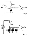
- the schematic circuit diagram in figure 1 illustrates a common way of biasing a capacitive microphone 1 having a static capacitance value C by use of a bias resistor 2 (R bias ) connected in series with a DC reference voltage 3 (V ref ).
- the value of the bias resistor 2 is chosen such that the cut-off frequency of the sensor and bias resistor combination (determined by the inverse of the time constant of R bias C) is well below the frequency band of interest, in this case the audio band.
- the capacitor is charged to the bias voltage V ref and, although the capacitance value changes ( ⁇ C) according to varying sound pressure exciting the microphone, very little current leaks out of the capacitor 1 due to the high value of R bias (which is typically of the order of 100 M ⁇ or higher).
- a problem with the conventional biasing scheme shown in figure 1 is its sensitivity to parasitic capacitances at the output of the microphone.
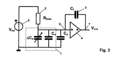
- An illustration of this is shown in the schematic circuit diagram of figure 2 , in which the microphone capacitance is shown divided into a constant part C s and a varying part ⁇ C s , with an additional parasitic capacitance given by a further parallel capacitance value C p .
- any parasitic capacitance at the connection of the microphone to the amplifier 4 also reduces this sensitivity.
- the input capacitance of the amplifier 4 connected to the output of the microphone reduces sensitivity even further (for simplicity this can be assumed to be also included in the parasitic capacitance C p shown in figure 2 ).
- This results in the following relationship for the voltage signal ⁇ V 1 input to the amplifier 4: ⁇ ⁇ V 1 ⁇ ⁇ C s ⁇ V ref ⁇ ⁇ C s ⁇ + C s ⁇ + C p
- the magnitude of the voltage signal ⁇ V 1 is therefore reduced according to the magnitude of the static capacitance C s of the capacitive sensor and by the total magnitude C p of any parasitic capacitances. This results in a reduced sensitivity, which will need to be compensated for by increasing the amplification factor of the amplifier 4, which can result in increased noise.
- a capacitive sensor amplifier circuit comprising:
- An advantage of the invention is that the feedback capacitor is connected across the amplifier such that it effectively counteracts or cancels part of the static capacitance of the capacitive sensor and any parasitic capacitance at the input of the amplifier. The sensitivity of the sensor is thereby increased.
- a value C f of the feedback capacitor can be selected such that (A-1)C f is within 10%, but is not equal to, a capacitance value given by C s + Cp, where A is an amplification factor of the amplifier, C s is a static capacitance value of the capacitive sensor and C p is a sum total of parasitic capacitances at the input of the amplifier.
- the value of (A-1)C f is equal or greater than 0.9(C s +C p ) while being less than C s + C p .
- An advantage of selecting the value of the feedback capacitor in this way is that the sensitivity of the sensor is maximised according to the value of the capacitance of the sensor and any associated parasitic capacitances. This also reduces the need to minimise parasitic capacitances, since the feedback capacitor can be chosen to counteract these, allowing a circuit design more flexibility.
- the input and output of the amplifier are both non-inverting. In alternative embodiments, the input and output are both inverting.
- the invention is particularly suitable for the capacitive sensor capacitive sensor being an acoustic sensor, but may also be applied to other types of capacitive sensors.
- a feedback capacitor 5 (C f ) is connected across the amplifier, using positive feedback, i.e. one plate of the feedback capacitor is connected to the non-inverting input 6 of the amplifier 4 and the other plate is connected to the non-inverting output 7 of the amplifier 4.
- the feedback capacitor may be connected between an inverting input of the amplifier and an inverting output of the amplifier.
- the feedback capacitor is connected between an input and an output of the amplifier where the input and output are of the same sign.
- the amplifier 4 operates like a Miller-type operational amplifier, but with positive feedback.
- the combination of the amplifier 4 and feedback capacitor 5 results in an effective negative capacitance at the input 6 of the amplifier 4. This negative capacitance therefore is subtracted from the static and parasitic capacitances C s , Cp at the amplifier input 6.
- Equation 2 above shows that the result of adding capacitive positive feedback to the amplifier is that when (A-1)C f is slightly smaller or larger than C s + C p , the output signal ⁇ V 2 can be increased substantially. However, when (A-1)C f is exactly equal to C s + C p the output signal ⁇ V 2 reduces to zero, which is of course unwanted.
- the value of C f should therefore be selected such that (A-1)C f is close to, but not equal to, the sum of the static capacitance of the capacitive sensor and any parasitic capacitances. In practical embodiments, (A-1)C f is preferably within 10%, i.e. is no more than 110% and no less than 90%, of C s + C p .
- (A-1)C f is equal to or greater than 0.9(C s + C p ) but is less than C s + C p , or alternatively is equal to or less than 1.1(C s + C p ) but is greater than C s + C p .
- One way of ensuring that this range is maintained is by selecting the value of C f such that a total spread of expected values for (A-1)C f , taking into account known statistical variations, remains within the above ranges, for example by selecting C f such that a 6 ⁇ spread of values for (A-1)C f remains within the range between 0.9(C s + C p ) and C s + C p or between 1.1(C s + C p ) and C s + C p .
- Equation shows the improvement, G boost , of the signal ⁇ V at the amplifier input 6, by comparing the value of ⁇ V 1 from equation 1 with ⁇ V 2 from equation 2:
- interference sources include switched mode voltage supplies, ground plane interference and electromagnetic interference.
- the signal boosting technique of the invention is not necessarily limited to only microphones, but can also be used for other types of capacitive sensors, examples including pressure sensors, ultrasound sensors (including ultrasound sensor arrays), distance sensors and accelerometers.
Landscapes
- Engineering & Computer Science (AREA)
- Power Engineering (AREA)
- Physics & Mathematics (AREA)
- Acoustics & Sound (AREA)
- Signal Processing (AREA)
- Multimedia (AREA)
- Amplifiers (AREA)
- Circuit For Audible Band Transducer (AREA)
Abstract
Description
- The invention relates to amplification of signals from capacitive sensors.
- Capacitive sensors such as capacitor-type microphones respond to received signals by a change in capacitance. This change in capacitance can be transformed into a voltage signal by applying a bias voltage across the capacitive element of the sensor and amplifying a voltage variation across the capacitive element resulting from the received signal.
- The schematic circuit diagram in
figure 1 illustrates a common way of biasing acapacitive microphone 1 having a static capacitance value C by use of a bias resistor 2 (Rbias) connected in series with a DC reference voltage 3 (Vref). The value of thebias resistor 2 is chosen such that the cut-off frequency of the sensor and bias resistor combination (determined by the inverse of the time constant of RbiasC) is well below the frequency band of interest, in this case the audio band. The capacitor is charged to the bias voltage Vref and, although the capacitance value changes (ΔC) according to varying sound pressure exciting the microphone, very little current leaks out of thecapacitor 1 due to the high value of Rbias (which is typically of the order of 100 MΩ or higher). The actual charge on the capacitor 1 (given by Q=VC) therefore stays almost constant, meaning that the output voltage of the microphone changes as a function of the incoming sound pressure level. Anamplifier 4 is connected to thecapacitor 1 to amplify this output voltage signal to provide an amplified output signal Vout. - A problem with the conventional biasing scheme shown in
figure 1 is its sensitivity to parasitic capacitances at the output of the microphone. An illustration of this is shown in the schematic circuit diagram offigure 2 , in which the microphone capacitance is shown divided into a constant part Cs and a varying part ΔCs, with an additional parasitic capacitance given by a further parallel capacitance value Cp. In typical microphones the varying part of the capacitance ΔCs is very small compared to its fixed part Cs. This results in a smaller output voltage change at the output of the microphone, as charge redistribution takes place in a larger capacitance (V=Q/C). Moreover, as the connection between the microphone output and associated electronics tend not to be on the same chip or circuit board, any parasitic capacitance at the connection of the microphone to theamplifier 4 also reduces this sensitivity. The input capacitance of theamplifier 4 connected to the output of the microphone reduces sensitivity even further (for simplicity this can be assumed to be also included in the parasitic capacitance Cp shown infigure 2 ). This results in the following relationship for the voltage signal ΔV1 input to the amplifier 4:
- The magnitude of the voltage signal ΔV1 is therefore reduced according to the magnitude of the static capacitance Cs of the capacitive sensor and by the total magnitude Cp of any parasitic capacitances. This results in a reduced sensitivity, which will need to be compensated for by increasing the amplification factor of the
amplifier 4, which can result in increased noise. - It is an object of the invention to address the above mentioned problem.
- In accordance with the invention there is provided a capacitive sensor amplifier circuit comprising:
- a capacitive sensor;
- a bias voltage supply connected across the capacitive sensor via a bias resistor;
- an operational amplifier having an input connected to the capacitive sensor; and
- a feedback capacitor connected between the input and an output of the amplifier, the input and output being of the same sign.
- An advantage of the invention is that the feedback capacitor is connected across the amplifier such that it effectively counteracts or cancels part of the static capacitance of the capacitive sensor and any parasitic capacitance at the input of the amplifier. The sensitivity of the sensor is thereby increased.
- A value Cf of the feedback capacitor can be selected such that (A-1)Cf is within 10%, but is not equal to, a capacitance value given by Cs + Cp, where A is an amplification factor of the amplifier, Cs is a static capacitance value of the capacitive sensor and Cp is a sum total of parasitic capacitances at the input of the amplifier.
- In certain embodiments, the value of (A-1)Cf is equal or greater than 0.9(Cs+Cp) while being less than Cs+ Cp.
- An advantage of selecting the value of the feedback capacitor in this way is that the sensitivity of the sensor is maximised according to the value of the capacitance of the sensor and any associated parasitic capacitances. This also reduces the need to minimise parasitic capacitances, since the feedback capacitor can be chosen to counteract these, allowing a circuit design more flexibility.
- In preferred embodiments, the input and output of the amplifier are both non-inverting. In alternative embodiments, the input and output are both inverting.
- The invention is particularly suitable for the capacitive sensor capacitive sensor being an acoustic sensor, but may also be applied to other types of capacitive sensors.
- The invention is described in further detail below by way of example, with reference to the appended drawings in which:
-
figure 1 is a schematic circuit diagram of a known type of capacitive sensor amplifier circuit; -
figure 2 is an alternative schematic circuit diagram of the circuit offigure 1 ; and -
figure 3 is a schematic circuit diagram of a capacitive sensor amplifier circuit according to an embodiment of the invention. -
Figures 1 and 2 have already been described above in the background to the invention. - An embodiment of the invention is illustrated in the schematic circuit diagram in
figure 3 . A feedback capacitor 5 (Cf) is connected across the amplifier, using positive feedback, i.e. one plate of the feedback capacitor is connected to thenon-inverting input 6 of theamplifier 4 and the other plate is connected to thenon-inverting output 7 of theamplifier 4. In alternative embodiments, the feedback capacitor may be connected between an inverting input of the amplifier and an inverting output of the amplifier. In a general aspect therefore, the feedback capacitor is connected between an input and an output of the amplifier where the input and output are of the same sign. - Other known arrangements in which a capacitor is provided in a feedback loop across an operational amplifier for amplifying signals from a capacitive sensor are known, such as disclosed in
US applications 2008/025531 and2009/086992 . Such arrangements, in which the feedback capacitor is connected between an inverting input and a non-inverting output of the amplifier, do not result in the cancellation property of the present invention, as described below. - By using a positive feedback loop, part of the output voltage signal Vout is fed back to the
capacitive sensor 1. Theamplifier 4 operates like a Miller-type operational amplifier, but with positive feedback. The combination of theamplifier 4 andfeedback capacitor 5 results in an effective negative capacitance at theinput 6 of theamplifier 4. This negative capacitance therefore is subtracted from the static and parasitic capacitances Cs, Cp at theamplifier input 6. The voltage signal ΔV2 at theamplifier input 6 is consequently boosted, according to the following relationship:
where A is the amplification factor of theamplifier 4. -
Equation 2 above shows that the result of adding capacitive positive feedback to the amplifier is that when (A-1)Cf is slightly smaller or larger than Cs + Cp, the output signal ΔV2 can be increased substantially. However, when (A-1)Cf is exactly equal to Cs + Cp the output signal ΔV2 reduces to zero, which is of course unwanted. The value of Cf should therefore be selected such that (A-1)Cf is close to, but not equal to, the sum of the static capacitance of the capacitive sensor and any parasitic capacitances. In practical embodiments, (A-1)Cf is preferably within 10%, i.e. is no more than 110% and no less than 90%, of Cs + Cp. In certain embodiments, (A-1)Cf is equal to or greater than 0.9(Cs + Cp) but is less than Cs + Cp, or alternatively is equal to or less than 1.1(Cs + Cp) but is greater than Cs + Cp. One way of ensuring that this range is maintained is by selecting the value of Cf such that a total spread of expected values for (A-1)Cf, taking into account known statistical variations, remains within the above ranges, for example by selecting Cf such that a 6σ spread of values for (A-1)Cf remains within the range between 0.9(Cs + Cp) and Cs+ Cp or between 1.1(Cs + Cp) and Cs+ Cp. - The following equation shows the improvement, Gboost, of the signal ΔV at the
amplifier input 6, by comparing the value of ΔV1 fromequation 1 with ΔV2 from equation 2:
- Because this signal boosting results in a larger magnitude of signal at the microphone output and
amplifier input 6, the signal becomes much more robust to interference. Examples of interference sources include switched mode voltage supplies, ground plane interference and electromagnetic interference. - The signal boosting technique of the invention is not necessarily limited to only microphones, but can also be used for other types of capacitive sensors, examples including pressure sensors, ultrasound sensors (including ultrasound sensor arrays), distance sensors and accelerometers.
- Other embodiments are also within the scope of the invention, as defined by the appended claims.
Claims (5)
- A capacitive sensor amplifier circuit comprising:a capacitive sensor (1);a bias voltage supply (3) connected across the capacitive sensor (1) via a bias resistor (2);an operational amplifier (4) having an input connected to the capacitive sensor (1); anda feedback capacitor (5) connected between the input and an output of the amplifier (4), the input and output being of the same sign.
- The capacitive sensor amplifier circuit of claim 1 wherein a value Cf of the feedback capacitor (5) is selected such that (A-1)Cf is within 10% of, but is not equal to, a capacitance value given by Cs + Cp, where A is an amplification factor of the amplifier (4), Cs is a static capacitance value of the capacitive sensor (1) and Cp is a sum total of parasitic capacitances at the input of the amplifier (4).
- The capacitive sensor amplifier circuit of claim 2 wherein the value of the feedback capacitor (5) is selected such that 0.9 (Cs + Cp) ≤ (A-1)Cf < Cs + Cp.
- The capacitive sensor amplifier circuit of any preceding claim wherein the input (6) is a non-inverting input.
- The capacitive sensor amplifier circuit of any preceding claim wherein the capacitive sensor (1) is an acoustic sensor.
Priority Applications (3)
| Application Number | Priority Date | Filing Date | Title |
|---|---|---|---|
| EP09252438.8A EP2317645B1 (en) | 2009-10-16 | 2009-10-16 | Capacitive sensor |
| CN201010512715.7A CN102045630B (en) | 2009-10-16 | 2010-10-08 | Capacitive sensor |
| US12/905,677 US8242840B2 (en) | 2009-10-16 | 2010-10-15 | Capacitive sensor |
Applications Claiming Priority (1)
| Application Number | Priority Date | Filing Date | Title |
|---|---|---|---|
| EP09252438.8A EP2317645B1 (en) | 2009-10-16 | 2009-10-16 | Capacitive sensor |
Publications (2)
| Publication Number | Publication Date |
|---|---|
| EP2317645A1 true EP2317645A1 (en) | 2011-05-04 |
| EP2317645B1 EP2317645B1 (en) | 2013-04-10 |
Family
ID=41625990
Family Applications (1)
| Application Number | Title | Priority Date | Filing Date |
|---|---|---|---|
| EP09252438.8A Not-in-force EP2317645B1 (en) | 2009-10-16 | 2009-10-16 | Capacitive sensor |
Country Status (3)
| Country | Link |
|---|---|
| US (1) | US8242840B2 (en) |
| EP (1) | EP2317645B1 (en) |
| CN (1) | CN102045630B (en) |
Cited By (4)
| Publication number | Priority date | Publication date | Assignee | Title |
|---|---|---|---|---|
| EP2675188A1 (en) * | 2012-06-12 | 2013-12-18 | austriamicrosystems AG | Sensor arrangement and method for generating an amplified sensor signal |
| CN110445470A (en) * | 2015-05-29 | 2019-11-12 | 意法半导体股份有限公司 | Differential amplifier circuit and corresponding capacitor sonic transducer for capacitor sonic transducer |
| WO2020036702A1 (en) * | 2018-08-14 | 2020-02-20 | Invensense, Inc. | Applying a positive feedback voltage to an electromechanical sensor utilizing a voltage-to-voltage converter to facilitate a reduction of charge flow in such sensor representing spring softening |
| WO2020037067A1 (en) * | 2018-08-14 | 2020-02-20 | Invensense, Inc. | Applying a positive feedback voltage to an electromechanical sensor utilizing a voltage-to-voltage converter to facilitate a reduction of charge flow in such sensor representing spring softening |
Families Citing this family (10)
| Publication number | Priority date | Publication date | Assignee | Title |
|---|---|---|---|---|
| US8630429B2 (en) * | 2011-12-16 | 2014-01-14 | Robert Bosch Gmbh | Preventing electrostatic pull-in in capacitive devices |
| US8884699B2 (en) * | 2012-12-18 | 2014-11-11 | Maxim Integrated Products, Inc. | Input common mode control using a dedicated comparator for sensor interfaces |
| KR101475263B1 (en) | 2013-05-22 | 2014-12-22 | 주식회사 씨자인 | Startup circuit, amplifying device for capacitor sensor having the startup circuit and startup method therefor |
| IT201600103234A1 (en) | 2016-10-14 | 2018-04-14 | Green Seas Ventures Ldt | Constructive system relating to a capacitive voltage sensor |
| EP3404422B1 (en) * | 2017-05-19 | 2019-11-13 | NXP USA, Inc. | System including a capacitive transducer and an excitation circuit for such a transducer and a method for measuring acceleration with such a system |
| IT201800004114A1 (en) | 2018-03-30 | 2019-09-30 | Green Seas Ventures Ltd C/O Citco B V I Ltd | CONSTRUCTION SYSTEM WITH A CAPACITIVE VOLTAGE SENSOR |
| JP7410935B2 (en) | 2018-05-24 | 2024-01-10 | ザ リサーチ ファウンデーション フォー ザ ステイト ユニバーシティー オブ ニューヨーク | capacitive sensor |
| CN119986166A (en) | 2018-12-17 | 2025-05-13 | G&W电气公司 | Electrical sensor assembly |
| US11340266B2 (en) | 2018-12-17 | 2022-05-24 | G & W Electric Company | Electrical sensor assembly |
| CN114915267A (en) * | 2022-04-19 | 2022-08-16 | 瑞声声学科技(深圳)有限公司 | Single-end-to-differential microphone circuit and electronic equipment |
Citations (5)
| Publication number | Priority date | Publication date | Assignee | Title |
|---|---|---|---|---|
| WO1994023547A1 (en) * | 1993-04-07 | 1994-10-13 | A/S Brüel & Kjær | A method and a coupling for reducing the harmonic distortion of a capacitive transducer |
| DE19600689A1 (en) * | 1995-01-11 | 1996-07-25 | Yoshiro Tomikawa | Capacitive component reduction circuit e.g. in electrostatic converter |
| EP1739826A1 (en) * | 2005-07-01 | 2007-01-03 | The Alfred E Mann Foundation for Scientific Research | Ultra low-frequency response, dc-blocked low-noise amplifier |
| US20080025531A1 (en) | 2006-07-25 | 2008-01-31 | Sanyo Electric Co., Ltd. | Microphone amplifier |
| US20090086992A1 (en) | 2007-09-27 | 2009-04-02 | Fortemedia, Inc. | Microphone circuit and charge amplifier thereof |
Family Cites Families (2)
| Publication number | Priority date | Publication date | Assignee | Title |
|---|---|---|---|---|
| DE19949985C2 (en) * | 1999-10-15 | 2001-08-16 | Sie Sensorik Ind Elektronik Gm | Capacitive sensor for the detection of the level of a medium in a container |
| GB2441360B (en) * | 2006-08-31 | 2011-09-21 | Wolfson Microelectronics Plc | Amplifier apparatus and method |
-
2009
- 2009-10-16 EP EP09252438.8A patent/EP2317645B1/en not_active Not-in-force
-
2010
- 2010-10-08 CN CN201010512715.7A patent/CN102045630B/en not_active Expired - Fee Related
- 2010-10-15 US US12/905,677 patent/US8242840B2/en active Active
Patent Citations (5)
| Publication number | Priority date | Publication date | Assignee | Title |
|---|---|---|---|---|
| WO1994023547A1 (en) * | 1993-04-07 | 1994-10-13 | A/S Brüel & Kjær | A method and a coupling for reducing the harmonic distortion of a capacitive transducer |
| DE19600689A1 (en) * | 1995-01-11 | 1996-07-25 | Yoshiro Tomikawa | Capacitive component reduction circuit e.g. in electrostatic converter |
| EP1739826A1 (en) * | 2005-07-01 | 2007-01-03 | The Alfred E Mann Foundation for Scientific Research | Ultra low-frequency response, dc-blocked low-noise amplifier |
| US20080025531A1 (en) | 2006-07-25 | 2008-01-31 | Sanyo Electric Co., Ltd. | Microphone amplifier |
| US20090086992A1 (en) | 2007-09-27 | 2009-04-02 | Fortemedia, Inc. | Microphone circuit and charge amplifier thereof |
Cited By (15)
| Publication number | Priority date | Publication date | Assignee | Title |
|---|---|---|---|---|
| US10823774B2 (en) | 2012-06-12 | 2020-11-03 | Ams Ag | Sensor arrangement with a capacitive sensor and method for generating an amplified sensor signal with a capacitive sensor |
| EP2675188A1 (en) * | 2012-06-12 | 2013-12-18 | austriamicrosystems AG | Sensor arrangement and method for generating an amplified sensor signal |
| EP2955936A1 (en) * | 2012-06-12 | 2015-12-16 | ams AG | Sensor arrangement and method for generating an amplified sensor signal |
| EP3229493A1 (en) * | 2012-06-12 | 2017-10-11 | ams AG | Sensor arrangement and method for generating an amplified sensor signal |
| US10222407B2 (en) | 2012-06-12 | 2019-03-05 | Ams Ag | Sensor arrangement with a capacitive sensor and method for generating an amplified sensor signal with a capacitive sensor |
| EP3509323A1 (en) * | 2012-06-12 | 2019-07-10 | ams AG | Sensor arrangement and method for generating an amplified sensor signal |
| WO2013185988A1 (en) * | 2012-06-12 | 2013-12-19 | Ams Ag | Sensor arrangement and method for generating an amplified sensor signal |
| CN110445470B (en) * | 2015-05-29 | 2024-11-05 | 意法半导体股份有限公司 | Differential amplifier circuit for capacitive acoustic transducer and corresponding capacitive acoustic transducer |
| CN110445470A (en) * | 2015-05-29 | 2019-11-12 | 意法半导体股份有限公司 | Differential amplifier circuit and corresponding capacitor sonic transducer for capacitor sonic transducer |
| CN112840560A (en) * | 2018-08-14 | 2021-05-25 | 因文森斯公司 | A positive feedback voltage is applied to the electromechanical sensor using a voltage-to-voltage converter to promote a reduction in the flow of charge in the sensor indicative of spring softening |
| WO2020036702A1 (en) * | 2018-08-14 | 2020-02-20 | Invensense, Inc. | Applying a positive feedback voltage to an electromechanical sensor utilizing a voltage-to-voltage converter to facilitate a reduction of charge flow in such sensor representing spring softening |
| US11085770B2 (en) | 2018-08-14 | 2021-08-10 | Invensense, Inc. | Applying a positive feedback voltage to an electromechanical sensor utilizing a voltage-to-voltage converter to facilitate a reduction of charge flow in such sensor representing spring softening |
| US11428702B2 (en) | 2018-08-14 | 2022-08-30 | Invensense, Inc. | Applying a positive feedback voltage to an electromechanical sensor utilizing a voltage-to-voltage converter to facilitate a reduction of charge flow in such sensor representing spring |
| US11835538B2 (en) | 2018-08-14 | 2023-12-05 | Invensense, Inc. | Applying a positive feedback voltage to an electromechanical sensor utilizing a voltage-to-voltage converter to facilitate a reduction of charge flow in such sensor representing spring softening |
| WO2020037067A1 (en) * | 2018-08-14 | 2020-02-20 | Invensense, Inc. | Applying a positive feedback voltage to an electromechanical sensor utilizing a voltage-to-voltage converter to facilitate a reduction of charge flow in such sensor representing spring softening |
Also Published As
| Publication number | Publication date |
|---|---|
| US20110090009A1 (en) | 2011-04-21 |
| CN102045630B (en) | 2013-09-18 |
| EP2317645B1 (en) | 2013-04-10 |
| US8242840B2 (en) | 2012-08-14 |
| CN102045630A (en) | 2011-05-04 |
Similar Documents
| Publication | Publication Date | Title |
|---|---|---|
| EP2317645B1 (en) | Capacitive sensor | |
| US8666095B2 (en) | Fast precision charge pump | |
| EP1742506B1 (en) | Microphone assembly with P-type preamplifier input stage | |
| US20090086992A1 (en) | Microphone circuit and charge amplifier thereof | |
| EP2982996B1 (en) | Dummy load circuit and charge detection circuit | |
| US8774428B2 (en) | Very low power MEMS microphone | |
| US10440482B2 (en) | Biasing of electromechanical systems transducer with alternating-current voltage waveform | |
| US20090285412A1 (en) | Integrated circuit biasing a microphone | |
| US9306449B2 (en) | Adjustable biasing circuits for MEMS capacitive microphones | |
| TWI652896B (en) | Mems sensor | |
| US20090052696A1 (en) | Electroacoustic transducer | |
| US10194240B2 (en) | Microphone assembly and method of reducing a temperature dependency of a microphone assembly | |
| JP2017096886A (en) | Piezoelectric sensor | |
| JP6368591B2 (en) | Charge amplifier circuit | |
| JPH08509327A (en) | Method and circuit configuration for reducing harmonic distortion of a capacitive transducer | |
| KR20130044576A (en) | Sound detect circuit and amplifier circuit thereof | |
| CN107968971B (en) | Microphone circuit | |
| CN110545503A (en) | Signal transmission circuit and signal transmission method | |
| US20110204972A1 (en) | Amplifying circuit | |
| US12506449B2 (en) | Amplifier for a dual backplate MEMS microphone |
Legal Events
| Date | Code | Title | Description |
|---|---|---|---|
| PUAI | Public reference made under article 153(3) epc to a published international application that has entered the european phase |
Free format text: ORIGINAL CODE: 0009012 |
|
| AK | Designated contracting states |
Kind code of ref document: A1 Designated state(s): AT BE BG CH CY CZ DE DK EE ES FI FR GB GR HR HU IE IS IT LI LT LU LV MC MK MT NL NO PL PT RO SE SI SK SM TR |
|
| AX | Request for extension of the european patent |
Extension state: AL BA RS |
|
| 17P | Request for examination filed |
Effective date: 20111104 |
|
| GRAP | Despatch of communication of intention to grant a patent |
Free format text: ORIGINAL CODE: EPIDOSNIGR1 |
|
| GRAS | Grant fee paid |
Free format text: ORIGINAL CODE: EPIDOSNIGR3 |
|
| GRAA | (expected) grant |
Free format text: ORIGINAL CODE: 0009210 |
|
| AK | Designated contracting states |
Kind code of ref document: B1 Designated state(s): AT BE BG CH CY CZ DE DK EE ES FI FR GB GR HR HU IE IS IT LI LT LU LV MC MK MT NL NO PL PT RO SE SI SK SM TR |
|
| REG | Reference to a national code |
Ref country code: GB Ref legal event code: FG4D |
|
| REG | Reference to a national code |
Ref country code: AT Ref legal event code: REF Ref document number: 606478 Country of ref document: AT Kind code of ref document: T Effective date: 20130415 Ref country code: CH Ref legal event code: EP |
|
| REG | Reference to a national code |
Ref country code: IE Ref legal event code: FG4D |
|
| REG | Reference to a national code |
Ref country code: DE Ref legal event code: R096 Ref document number: 602009014808 Country of ref document: DE Effective date: 20130606 |
|
| PG25 | Lapsed in a contracting state [announced via postgrant information from national office to epo] |
Ref country code: SI Free format text: LAPSE BECAUSE OF FAILURE TO SUBMIT A TRANSLATION OF THE DESCRIPTION OR TO PAY THE FEE WITHIN THE PRESCRIBED TIME-LIMIT Effective date: 20130410 |
|
| REG | Reference to a national code |
Ref country code: AT Ref legal event code: MK05 Ref document number: 606478 Country of ref document: AT Kind code of ref document: T Effective date: 20130410 |
|
| REG | Reference to a national code |
Ref country code: LT Ref legal event code: MG4D Ref country code: NL Ref legal event code: VDEP Effective date: 20130410 |
|
| PG25 | Lapsed in a contracting state [announced via postgrant information from national office to epo] |
Ref country code: NO Free format text: LAPSE BECAUSE OF FAILURE TO SUBMIT A TRANSLATION OF THE DESCRIPTION OR TO PAY THE FEE WITHIN THE PRESCRIBED TIME-LIMIT Effective date: 20130710 Ref country code: AT Free format text: LAPSE BECAUSE OF FAILURE TO SUBMIT A TRANSLATION OF THE DESCRIPTION OR TO PAY THE FEE WITHIN THE PRESCRIBED TIME-LIMIT Effective date: 20130410 Ref country code: SE Free format text: LAPSE BECAUSE OF FAILURE TO SUBMIT A TRANSLATION OF THE DESCRIPTION OR TO PAY THE FEE WITHIN THE PRESCRIBED TIME-LIMIT Effective date: 20130410 Ref country code: GR Free format text: LAPSE BECAUSE OF FAILURE TO SUBMIT A TRANSLATION OF THE DESCRIPTION OR TO PAY THE FEE WITHIN THE PRESCRIBED TIME-LIMIT Effective date: 20130711 Ref country code: LT Free format text: LAPSE BECAUSE OF FAILURE TO SUBMIT A TRANSLATION OF THE DESCRIPTION OR TO PAY THE FEE WITHIN THE PRESCRIBED TIME-LIMIT Effective date: 20130410 Ref country code: IS Free format text: LAPSE BECAUSE OF FAILURE TO SUBMIT A TRANSLATION OF THE DESCRIPTION OR TO PAY THE FEE WITHIN THE PRESCRIBED TIME-LIMIT Effective date: 20130810 Ref country code: NL Free format text: LAPSE BECAUSE OF FAILURE TO SUBMIT A TRANSLATION OF THE DESCRIPTION OR TO PAY THE FEE WITHIN THE PRESCRIBED TIME-LIMIT Effective date: 20130410 Ref country code: ES Free format text: LAPSE BECAUSE OF FAILURE TO SUBMIT A TRANSLATION OF THE DESCRIPTION OR TO PAY THE FEE WITHIN THE PRESCRIBED TIME-LIMIT Effective date: 20130721 Ref country code: BE Free format text: LAPSE BECAUSE OF FAILURE TO SUBMIT A TRANSLATION OF THE DESCRIPTION OR TO PAY THE FEE WITHIN THE PRESCRIBED TIME-LIMIT Effective date: 20130410 Ref country code: FI Free format text: LAPSE BECAUSE OF FAILURE TO SUBMIT A TRANSLATION OF THE DESCRIPTION OR TO PAY THE FEE WITHIN THE PRESCRIBED TIME-LIMIT Effective date: 20130410 Ref country code: PT Free format text: LAPSE BECAUSE OF FAILURE TO SUBMIT A TRANSLATION OF THE DESCRIPTION OR TO PAY THE FEE WITHIN THE PRESCRIBED TIME-LIMIT Effective date: 20130812 |
|
| PG25 | Lapsed in a contracting state [announced via postgrant information from national office to epo] |
Ref country code: PL Free format text: LAPSE BECAUSE OF FAILURE TO SUBMIT A TRANSLATION OF THE DESCRIPTION OR TO PAY THE FEE WITHIN THE PRESCRIBED TIME-LIMIT Effective date: 20130410 Ref country code: BG Free format text: LAPSE BECAUSE OF FAILURE TO SUBMIT A TRANSLATION OF THE DESCRIPTION OR TO PAY THE FEE WITHIN THE PRESCRIBED TIME-LIMIT Effective date: 20130710 Ref country code: LV Free format text: LAPSE BECAUSE OF FAILURE TO SUBMIT A TRANSLATION OF THE DESCRIPTION OR TO PAY THE FEE WITHIN THE PRESCRIBED TIME-LIMIT Effective date: 20130410 Ref country code: CY Free format text: LAPSE BECAUSE OF FAILURE TO SUBMIT A TRANSLATION OF THE DESCRIPTION OR TO PAY THE FEE WITHIN THE PRESCRIBED TIME-LIMIT Effective date: 20130410 Ref country code: HR Free format text: LAPSE BECAUSE OF FAILURE TO SUBMIT A TRANSLATION OF THE DESCRIPTION OR TO PAY THE FEE WITHIN THE PRESCRIBED TIME-LIMIT Effective date: 20130410 |
|
| PG25 | Lapsed in a contracting state [announced via postgrant information from national office to epo] |
Ref country code: SK Free format text: LAPSE BECAUSE OF FAILURE TO SUBMIT A TRANSLATION OF THE DESCRIPTION OR TO PAY THE FEE WITHIN THE PRESCRIBED TIME-LIMIT Effective date: 20130410 Ref country code: EE Free format text: LAPSE BECAUSE OF FAILURE TO SUBMIT A TRANSLATION OF THE DESCRIPTION OR TO PAY THE FEE WITHIN THE PRESCRIBED TIME-LIMIT Effective date: 20130410 Ref country code: DK Free format text: LAPSE BECAUSE OF FAILURE TO SUBMIT A TRANSLATION OF THE DESCRIPTION OR TO PAY THE FEE WITHIN THE PRESCRIBED TIME-LIMIT Effective date: 20130410 Ref country code: CZ Free format text: LAPSE BECAUSE OF FAILURE TO SUBMIT A TRANSLATION OF THE DESCRIPTION OR TO PAY THE FEE WITHIN THE PRESCRIBED TIME-LIMIT Effective date: 20130410 |
|
| PLBE | No opposition filed within time limit |
Free format text: ORIGINAL CODE: 0009261 |
|
| STAA | Information on the status of an ep patent application or granted ep patent |
Free format text: STATUS: NO OPPOSITION FILED WITHIN TIME LIMIT |
|
| PG25 | Lapsed in a contracting state [announced via postgrant information from national office to epo] |
Ref country code: RO Free format text: LAPSE BECAUSE OF FAILURE TO SUBMIT A TRANSLATION OF THE DESCRIPTION OR TO PAY THE FEE WITHIN THE PRESCRIBED TIME-LIMIT Effective date: 20130410 Ref country code: IT Free format text: LAPSE BECAUSE OF FAILURE TO SUBMIT A TRANSLATION OF THE DESCRIPTION OR TO PAY THE FEE WITHIN THE PRESCRIBED TIME-LIMIT Effective date: 20130410 |
|
| 26N | No opposition filed |
Effective date: 20140113 |
|
| REG | Reference to a national code |
Ref country code: DE Ref legal event code: R097 Ref document number: 602009014808 Country of ref document: DE Effective date: 20140113 |
|
| PG25 | Lapsed in a contracting state [announced via postgrant information from national office to epo] |
Ref country code: MC Free format text: LAPSE BECAUSE OF FAILURE TO SUBMIT A TRANSLATION OF THE DESCRIPTION OR TO PAY THE FEE WITHIN THE PRESCRIBED TIME-LIMIT Effective date: 20130410 |
|
| REG | Reference to a national code |
Ref country code: CH Ref legal event code: PL |
|
| REG | Reference to a national code |
Ref country code: IE Ref legal event code: MM4A |
|
| PG25 | Lapsed in a contracting state [announced via postgrant information from national office to epo] |
Ref country code: CH Free format text: LAPSE BECAUSE OF NON-PAYMENT OF DUE FEES Effective date: 20131031 Ref country code: LI Free format text: LAPSE BECAUSE OF NON-PAYMENT OF DUE FEES Effective date: 20131031 |
|
| PG25 | Lapsed in a contracting state [announced via postgrant information from national office to epo] |
Ref country code: IE Free format text: LAPSE BECAUSE OF NON-PAYMENT OF DUE FEES Effective date: 20131016 |
|
| PG25 | Lapsed in a contracting state [announced via postgrant information from national office to epo] |
Ref country code: SM Free format text: LAPSE BECAUSE OF FAILURE TO SUBMIT A TRANSLATION OF THE DESCRIPTION OR TO PAY THE FEE WITHIN THE PRESCRIBED TIME-LIMIT Effective date: 20130410 |
|
| PG25 | Lapsed in a contracting state [announced via postgrant information from national office to epo] |
Ref country code: TR Free format text: LAPSE BECAUSE OF FAILURE TO SUBMIT A TRANSLATION OF THE DESCRIPTION OR TO PAY THE FEE WITHIN THE PRESCRIBED TIME-LIMIT Effective date: 20130410 |
|
| PG25 | Lapsed in a contracting state [announced via postgrant information from national office to epo] |
Ref country code: LU Free format text: LAPSE BECAUSE OF NON-PAYMENT OF DUE FEES Effective date: 20131016 Ref country code: MK Free format text: LAPSE BECAUSE OF FAILURE TO SUBMIT A TRANSLATION OF THE DESCRIPTION OR TO PAY THE FEE WITHIN THE PRESCRIBED TIME-LIMIT Effective date: 20130410 Ref country code: HU Free format text: LAPSE BECAUSE OF FAILURE TO SUBMIT A TRANSLATION OF THE DESCRIPTION OR TO PAY THE FEE WITHIN THE PRESCRIBED TIME-LIMIT; INVALID AB INITIO Effective date: 20091016 |
|
| PG25 | Lapsed in a contracting state [announced via postgrant information from national office to epo] |
Ref country code: MT Free format text: LAPSE BECAUSE OF FAILURE TO SUBMIT A TRANSLATION OF THE DESCRIPTION OR TO PAY THE FEE WITHIN THE PRESCRIBED TIME-LIMIT Effective date: 20130410 |
|
| REG | Reference to a national code |
Ref country code: FR Ref legal event code: PLFP Year of fee payment: 8 |
|
| REG | Reference to a national code |
Ref country code: FR Ref legal event code: PLFP Year of fee payment: 9 |
|
| REG | Reference to a national code |
Ref country code: FR Ref legal event code: PLFP Year of fee payment: 10 |
|
| PGFP | Annual fee paid to national office [announced via postgrant information from national office to epo] |
Ref country code: FR Payment date: 20180920 Year of fee payment: 10 |
|
| PGFP | Annual fee paid to national office [announced via postgrant information from national office to epo] |
Ref country code: GB Payment date: 20180925 Year of fee payment: 10 |
|
| PGFP | Annual fee paid to national office [announced via postgrant information from national office to epo] |
Ref country code: DE Payment date: 20180819 Year of fee payment: 10 |
|
| REG | Reference to a national code |
Ref country code: DE Ref legal event code: R119 Ref document number: 602009014808 Country of ref document: DE |
|
| PG25 | Lapsed in a contracting state [announced via postgrant information from national office to epo] |
Ref country code: DE Free format text: LAPSE BECAUSE OF NON-PAYMENT OF DUE FEES Effective date: 20200501 |
|
| GBPC | Gb: european patent ceased through non-payment of renewal fee |
Effective date: 20191016 |
|
| PG25 | Lapsed in a contracting state [announced via postgrant information from national office to epo] |
Ref country code: FR Free format text: LAPSE BECAUSE OF NON-PAYMENT OF DUE FEES Effective date: 20191031 Ref country code: GB Free format text: LAPSE BECAUSE OF NON-PAYMENT OF DUE FEES Effective date: 20191016 |