EP2317493A1 - Display apparatus and manufacturing method therefor, and active matrix circuit board - Google Patents
Display apparatus and manufacturing method therefor, and active matrix circuit board Download PDFInfo
- Publication number
- EP2317493A1 EP2317493A1 EP09808011A EP09808011A EP2317493A1 EP 2317493 A1 EP2317493 A1 EP 2317493A1 EP 09808011 A EP09808011 A EP 09808011A EP 09808011 A EP09808011 A EP 09808011A EP 2317493 A1 EP2317493 A1 EP 2317493A1
- Authority
- EP
- European Patent Office
- Prior art keywords
- line
- lines
- display
- blocks
- broken
- Prior art date
- Legal status (The legal status is an assumption and is not a legal conclusion. Google has not performed a legal analysis and makes no representation as to the accuracy of the status listed.)
- Ceased
Links
Images




Classifications
-
- G—PHYSICS
- G09—EDUCATION; CRYPTOGRAPHY; DISPLAY; ADVERTISING; SEALS
- G09G—ARRANGEMENTS OR CIRCUITS FOR CONTROL OF INDICATING DEVICES USING STATIC MEANS TO PRESENT VARIABLE INFORMATION
- G09G3/00—Control arrangements or circuits, of interest only in connection with visual indicators other than cathode-ray tubes
- G09G3/006—Electronic inspection or testing of displays and display drivers, e.g. of LED or LCD displays
-
- G—PHYSICS
- G02—OPTICS
- G02F—OPTICAL DEVICES OR ARRANGEMENTS FOR THE CONTROL OF LIGHT BY MODIFICATION OF THE OPTICAL PROPERTIES OF THE MEDIA OF THE ELEMENTS INVOLVED THEREIN; NON-LINEAR OPTICS; FREQUENCY-CHANGING OF LIGHT; OPTICAL LOGIC ELEMENTS; OPTICAL ANALOGUE/DIGITAL CONVERTERS
- G02F1/00—Devices or arrangements for the control of the intensity, colour, phase, polarisation or direction of light arriving from an independent light source, e.g. switching, gating or modulating; Non-linear optics
- G02F1/01—Devices or arrangements for the control of the intensity, colour, phase, polarisation or direction of light arriving from an independent light source, e.g. switching, gating or modulating; Non-linear optics for the control of the intensity, phase, polarisation or colour
- G02F1/13—Devices or arrangements for the control of the intensity, colour, phase, polarisation or direction of light arriving from an independent light source, e.g. switching, gating or modulating; Non-linear optics for the control of the intensity, phase, polarisation or colour based on liquid crystals, e.g. single liquid crystal display cells
- G02F1/133—Constructional arrangements; Operation of liquid crystal cells; Circuit arrangements
- G02F1/136—Liquid crystal cells structurally associated with a semi-conducting layer or substrate, e.g. cells forming part of an integrated circuit
- G02F1/1362—Active matrix addressed cells
- G02F1/136259—Repairing; Defects
-
- G—PHYSICS
- G09—EDUCATION; CRYPTOGRAPHY; DISPLAY; ADVERTISING; SEALS
- G09G—ARRANGEMENTS OR CIRCUITS FOR CONTROL OF INDICATING DEVICES USING STATIC MEANS TO PRESENT VARIABLE INFORMATION
- G09G3/00—Control arrangements or circuits, of interest only in connection with visual indicators other than cathode-ray tubes
- G09G3/20—Control arrangements or circuits, of interest only in connection with visual indicators other than cathode-ray tubes for presentation of an assembly of a number of characters, e.g. a page, by composing the assembly by combination of individual elements arranged in a matrix no fixed position being assigned to or needed to be assigned to the individual characters or partial characters
- G09G3/34—Control arrangements or circuits, of interest only in connection with visual indicators other than cathode-ray tubes for presentation of an assembly of a number of characters, e.g. a page, by composing the assembly by combination of individual elements arranged in a matrix no fixed position being assigned to or needed to be assigned to the individual characters or partial characters by control of light from an independent source
- G09G3/36—Control arrangements or circuits, of interest only in connection with visual indicators other than cathode-ray tubes for presentation of an assembly of a number of characters, e.g. a page, by composing the assembly by combination of individual elements arranged in a matrix no fixed position being assigned to or needed to be assigned to the individual characters or partial characters by control of light from an independent source using liquid crystals
- G09G3/3611—Control of matrices with row and column drivers
-
- G—PHYSICS
- G02—OPTICS
- G02F—OPTICAL DEVICES OR ARRANGEMENTS FOR THE CONTROL OF LIGHT BY MODIFICATION OF THE OPTICAL PROPERTIES OF THE MEDIA OF THE ELEMENTS INVOLVED THEREIN; NON-LINEAR OPTICS; FREQUENCY-CHANGING OF LIGHT; OPTICAL LOGIC ELEMENTS; OPTICAL ANALOGUE/DIGITAL CONVERTERS
- G02F1/00—Devices or arrangements for the control of the intensity, colour, phase, polarisation or direction of light arriving from an independent light source, e.g. switching, gating or modulating; Non-linear optics
- G02F1/01—Devices or arrangements for the control of the intensity, colour, phase, polarisation or direction of light arriving from an independent light source, e.g. switching, gating or modulating; Non-linear optics for the control of the intensity, phase, polarisation or colour
- G02F1/13—Devices or arrangements for the control of the intensity, colour, phase, polarisation or direction of light arriving from an independent light source, e.g. switching, gating or modulating; Non-linear optics for the control of the intensity, phase, polarisation or colour based on liquid crystals, e.g. single liquid crystal display cells
- G02F1/133—Constructional arrangements; Operation of liquid crystal cells; Circuit arrangements
- G02F1/1333—Constructional arrangements; Manufacturing methods
- G02F1/133388—Constructional arrangements; Manufacturing methods with constructional differences between the display region and the peripheral region
-
- G—PHYSICS
- G02—OPTICS
- G02F—OPTICAL DEVICES OR ARRANGEMENTS FOR THE CONTROL OF LIGHT BY MODIFICATION OF THE OPTICAL PROPERTIES OF THE MEDIA OF THE ELEMENTS INVOLVED THEREIN; NON-LINEAR OPTICS; FREQUENCY-CHANGING OF LIGHT; OPTICAL LOGIC ELEMENTS; OPTICAL ANALOGUE/DIGITAL CONVERTERS
- G02F1/00—Devices or arrangements for the control of the intensity, colour, phase, polarisation or direction of light arriving from an independent light source, e.g. switching, gating or modulating; Non-linear optics
- G02F1/01—Devices or arrangements for the control of the intensity, colour, phase, polarisation or direction of light arriving from an independent light source, e.g. switching, gating or modulating; Non-linear optics for the control of the intensity, phase, polarisation or colour
- G02F1/13—Devices or arrangements for the control of the intensity, colour, phase, polarisation or direction of light arriving from an independent light source, e.g. switching, gating or modulating; Non-linear optics for the control of the intensity, phase, polarisation or colour based on liquid crystals, e.g. single liquid crystal display cells
- G02F1/133—Constructional arrangements; Operation of liquid crystal cells; Circuit arrangements
- G02F1/136—Liquid crystal cells structurally associated with a semi-conducting layer or substrate, e.g. cells forming part of an integrated circuit
- G02F1/1362—Active matrix addressed cells
- G02F1/136259—Repairing; Defects
- G02F1/136263—Line defects
-
- G—PHYSICS
- G02—OPTICS
- G02F—OPTICAL DEVICES OR ARRANGEMENTS FOR THE CONTROL OF LIGHT BY MODIFICATION OF THE OPTICAL PROPERTIES OF THE MEDIA OF THE ELEMENTS INVOLVED THEREIN; NON-LINEAR OPTICS; FREQUENCY-CHANGING OF LIGHT; OPTICAL LOGIC ELEMENTS; OPTICAL ANALOGUE/DIGITAL CONVERTERS
- G02F1/00—Devices or arrangements for the control of the intensity, colour, phase, polarisation or direction of light arriving from an independent light source, e.g. switching, gating or modulating; Non-linear optics
- G02F1/01—Devices or arrangements for the control of the intensity, colour, phase, polarisation or direction of light arriving from an independent light source, e.g. switching, gating or modulating; Non-linear optics for the control of the intensity, phase, polarisation or colour
- G02F1/13—Devices or arrangements for the control of the intensity, colour, phase, polarisation or direction of light arriving from an independent light source, e.g. switching, gating or modulating; Non-linear optics for the control of the intensity, phase, polarisation or colour based on liquid crystals, e.g. single liquid crystal display cells
- G02F1/133—Constructional arrangements; Operation of liquid crystal cells; Circuit arrangements
- G02F1/136—Liquid crystal cells structurally associated with a semi-conducting layer or substrate, e.g. cells forming part of an integrated circuit
- G02F1/1362—Active matrix addressed cells
- G02F1/136259—Repairing; Defects
- G02F1/136272—Auxiliary lines
-
- G—PHYSICS
- G09—EDUCATION; CRYPTOGRAPHY; DISPLAY; ADVERTISING; SEALS
- G09G—ARRANGEMENTS OR CIRCUITS FOR CONTROL OF INDICATING DEVICES USING STATIC MEANS TO PRESENT VARIABLE INFORMATION
- G09G2300/00—Aspects of the constitution of display devices
- G09G2300/04—Structural and physical details of display devices
- G09G2300/0421—Structural details of the set of electrodes
- G09G2300/0426—Layout of electrodes and connections
-
- G—PHYSICS
- G09—EDUCATION; CRYPTOGRAPHY; DISPLAY; ADVERTISING; SEALS
- G09G—ARRANGEMENTS OR CIRCUITS FOR CONTROL OF INDICATING DEVICES USING STATIC MEANS TO PRESENT VARIABLE INFORMATION
- G09G2330/00—Aspects of power supply; Aspects of display protection and defect management
- G09G2330/08—Fault-tolerant or redundant circuits, or circuits in which repair of defects is prepared
-
- Y—GENERAL TAGGING OF NEW TECHNOLOGICAL DEVELOPMENTS; GENERAL TAGGING OF CROSS-SECTIONAL TECHNOLOGIES SPANNING OVER SEVERAL SECTIONS OF THE IPC; TECHNICAL SUBJECTS COVERED BY FORMER USPC CROSS-REFERENCE ART COLLECTIONS [XRACs] AND DIGESTS
- Y10—TECHNICAL SUBJECTS COVERED BY FORMER USPC
- Y10T—TECHNICAL SUBJECTS COVERED BY FORMER US CLASSIFICATION
- Y10T29/00—Metal working
- Y10T29/49—Method of mechanical manufacture
- Y10T29/49002—Electrical device making
- Y10T29/49004—Electrical device making including measuring or testing of device or component part
Definitions
- the present disclosure relates to display apparatuses and methods for manufacturing the display apparatuses, and active matrix substrates. More particularly, the present disclosure relates to techniques of repairing a break in a line for display provided in an active matrix substrate and a display apparatus.
- a liquid crystal display apparatus includes, for example, an active matrix substrate and a counter substrate facing each other.
- the active matrix substrate includes, for example, lines for display (hereinafter referred to as display lines) including a plurality of gate lines extending in parallel with each other and a plurality of source lines extending in parallel with each other and in a direction perpendicular to the gate lines. Therefore, the liquid crystal display apparatus including the active matrix substrate has the following problem. If a break occurs in a display line, such as a gate line or a source line, a display signal is not supplied from a drive circuit to a portion farther than the break of the broken display line, resulting in a significant degradation in display quality.
- liquid crystal display apparatuses which include lines for repairing a broken line and amplifier circuits connected to the broken-line repairing lines, which are provided outside a display region for displaying an image (see, for example, Japanese Patent Publication Nos. 2000-321599 , H11-160677 , 2000-105576 , and 2008-58337 ).
- FIG. 11 is a plan view of a conventional liquid crystal display apparatus 150 corresponding to the plan view described in Japanese Patent Publication No. 2000-321599 ( figure 5 ), schematically showing a liquid crystal display element and drive circuit substrates provided around the element.
- the liquid crystal display apparatus 150 includes a liquid crystal display panel 140, three film substrates 141 attached to an upper end of the liquid crystal display panel 140, and a printed substrate 145 attached to upper ends of the film substrates 141.
- the liquid crystal display panel 140 includes, in a display region D, a plurality of source lines 103 extending in parallel with each other and a plurality of gate lines (not shown) extending in parallel with each other and in a direction perpendicular to the source lines 103.
- the source lines 103 are divided into blocks B1-B3 which are adjacent to each other and each include a plurality of the source lines 103.
- the source lines 103 in the respective blocks B1-B3 are each connected to a drive circuit (not shown) provided on the corresponding film substrate 141.
- the liquid crystal display panel 140 includes, outside the display region D, three on-panel first lines 101 c extending along an upper side of the display region D and intersecting upper end portions of the source lines 103 provided in the respective blocks B1-B3, and an L-shaped on-panel second line 101d extending along a left side and a bottom side of the display region D and intersecting lower end portions of the source lines 103.
- the printed substrate 145 includes three on-printed-substrate first lines 146 connected to the on-panel first lines 101c via on-film-substrate first lines 142 provided on the film substrates 141, respectively, an on-printed-substrate second line 147 intersecting upper end portions of the on-printed-substrate first lines 146 and connected to the on-panel second line 101d via an on-film-substrate second line 143 provided on the leftmost film substrate 141, and an amplifier circuit A provided in a left end portion of the on-printed-substrate second line 147.
- a display signal (source signal) is supplied from the drive circuit (not shown) provided on the film substrate 141 to a portion lower than the portion X of the source line 103 via the on-panel first line 101c of the block B2, the on-film-substrate first line 142 of the block B2, the on-printed-substrate first line 146 of the block B2, the on-printed-substrate second line 147, the amplifier circuit A, the on-film-substrate second line 143, and the on-panel second line 101d. Therefore, the source signal is supplied from the drive circuit to a portion farther than the break portion (the portion X) of the source line 103, whereby the break in the source line 103 can be repaired.
- the broken source line 103 is repaired in the liquid crystal display apparatus 150 by, for example, irradiating the intersections M1-M3 with laser light to establish conduction between each line.
- the intersections M1-M3 are provided on both the liquid crystal display panel 140 and the printed substrate 145, and therefore, a plurality of laser irradiation devices are required and conditions for irradiation with laser light are complicated, leading to an increase in manufacturing cost. Therefore, there is a room for improvement.
- the present disclosure has been made in view of the above problem.
- the detailed description describes implementations of a technique of easily repairing a break in a display line.
- first lines inserting end portions closer to drive circuits of display lines in respective blocks and insulated from the display lines, intersect a second line inserting end portions farther than the drive circuits of the display lines in all the blocks on a display panel and insulated from the display lines, where the first lines are insulated from the second line.
- an example display apparatus of the present disclosure includes a display panel having a display region including a plurality of blocks extending in parallel with each other.
- the display panel includes a plurality of display lines provided in each of the blocks and extending in parallel with each other and in a direction in which the blocks extend, a plurality of drive circuits each provided outside the display region for a corresponding one of the blocks and connected to the display lines in the corresponding block, a plurality of first lines each provided outside the display region for a corresponding one of the blocks and intersecting end portions closer to the corresponding drive circuit of the display lines in the corresponding block, the first lines being insulated from the display lines, and a second line provided outside the display region and intersecting end portions farther from the drive circuits of the display lines of all the blocks, the second line being insulated from the display lines.
- the second line is configured to intersect the first lines while being insulated from the first lines, and be supplied with a display signal from each of the drive circuits via an amplifier circuit.
- the first lines inserting the end portions closer to the drive circuits of the display lines extending in parallel with each other in the respective blocks, the first lines being insulated from the display lines, intersect the second line inserting the end portions farther than the drive circuits of the display lines in all the blocks, the second line being insulated from the display lines, where the first lines are insulated from the second line. Therefore, intersections of the first lines and the display lines in the respective blocks, intersections of the second line and the display lines in all the blocks, and intersections of the first lines and the second line are provided outside the display region of the display panel. Therefore, a broken display line can be repaired as follows.
- the second line is configured to be supplied with a display signal from each drive circuit via an amplifier circuit. Therefore, by establishing conduction between each line in the above-described manner, a display signal from a drive circuit is amplified by an amplifier circuit and then supplied to a portion farther than a break portion of a broken display line. As a result, when a broken display line is repaired, the display panel is the only target to be irradiated with laser light, and therefore, conditions for irradiation with the laser light are simplified, whereby the broken display line can be easily repaired.
- Japanese Patent Publication No. 2000-321599 ( FIG. 1 ) describes a technique of irradiating two points on a display panel with laser light to establish conduction between each line.
- a single line corresponding to the first line is provided for all blocks. Loads occur at capacitances at intersections of the line corresponding to the first line and a plurality of signal lines in all the blocks, likely leading to an increase in signal delay.
- the first line is provided for each block, and therefore, the signal delay can be reduced or prevented.
- the amplifier circuit may be provided in a portion of each of the first lines between an intersection of the first line and the second line and intersections of the first line and the corresponding display lines.
- the amplifier circuit is provided for each first line, i.e., for each block, and therefore, a difference between signal delays depending on the position of a block in which a break occurs can be reduced or prevented.
- Another example display apparatus of the present disclosure includes a display panel having a display region including a plurality of blocks extending in parallel with each other.
- the display panel includes a plurality of display lines provided in each of the blocks and extending in parallel with each other and in a direction in which the blocks extend, a plurality of drive circuits each provided outside the display region for a corresponding one of the blocks and connected to the display lines in the corresponding block, a plurality of first lines each provided outside the display region for a corresponding one of the blocks and intersecting end portions closer to the corresponding drive circuit of the display lines in the corresponding block, the first lines being insulated from the display lines, and a second line provided outside the display region and intersecting end portions farther from the drive circuits of the display lines of all the blocks, the second line being insulated from the display lines.
- the second line is configured to intersect the first lines while being insulated from the first lines, and an amplifier circuit is provided in each of the first lines.
- the first lines inserting the end portions closer to the drive circuits of the display lines extending in parallel with each other in the respective blocks, the first lines being insulated from the display lines, intersect the second line inserting the end portions farther than the drive circuits of the display lines in all the blocks, the second line being insulated from the display lines, where the first lines are insulated from the second line. Therefore, intersections of the first lines and the display lines in the respective blocks, intersections of the second line and the display lines in all the blocks, and intersections of the first lines and the second line are provided outside the display region of the display panel. Therefore, a broken display line can be repaired as follows.
- any one of all the display lines provided on the display panel is broken, an intersection of a portion closer to the driver circuit of the broken display line and the corresponding first line, an intersection of a portion farther from the driver circuit of the broken display line and the second line, and an intersection of the corresponding first line and the second line, i.e., only three portions of the display panel, are irradiated with laser light to establish conduction between each line.
- the amplifier circuit is provided in each first line. Therefore, by establishing conduction between each line in the above-described manner, a display signal from a drive circuit is amplified by an amplifier circuit and then supplied to a portion farther than a break portion of a broken display line.
- the display panel is the only target to be irradiated with laser light, and therefore, conditions for irradiation with the laser light are simplified, whereby the broken display line can be easily repaired.
- a portion of each of the first lines between an intersection of the first line and the second line and intersections of the first line and the corresponding display lines may make a detour to temporarily pass through a region farther from the display region.
- the display apparatus may include, for each of the blocks, a plurality of first terminals connected to the respective display lines, a second terminal connected to the second line, a third terminal connected to a preceding stage portion closer to the plurality of first terminals of a detour path of the corresponding first line, and a fourth terminal connected to a succeeding stage portion closer to the second terminal of the detour path of the corresponding first line, the first to fourth terminals being provided outside the display region.
- the first terminals connected to the respective display lines, the second terminal connected to the second line, the third terminal connected to the preceding stage portion closer to the first terminals of the detour path of the corresponding first line, and the fourth terminal connected to the succeeding stage portion closer to the second terminal of the detour path of the corresponding first line, are provided for each block.
- a connection state between the repaired display line and the corresponding first line and a connection state between the corresponding first line and the second line can be confirmed.
- the display apparatus may further include a plurality of film substrates each provided for a corresponding one of the blocks and attached to an end portion outside the display region of the display panel.
- the detour paths of the first lines may be provided on the respective film substrates.
- the first, second, third, and fourth terminals may be provided on each of the film substrates.
- the amplifier circuit may be incorporated in the drive circuit provided in each of the film substrates.
- the display apparatus may include a printed substrate attached to end portions farther from the display panel of the film substrates. On the printed substrate, lines each linking the preceding stage portion and the succeeding stage portion of the detour path of the corresponding first line may be provided.
- the line linking the preceding stage portion and the succeeding stage portion is provided on the printed substrate in the detour path of each first line. Therefore, the line layout of the film substrate can be simplified, and the film substrate can be common to identical display apparatuses or other display apparatuses.
- the plurality of display lines in each of the blocks may be divided into a plurality of line groups.
- the first lines may each be provided for a corresponding one of the line groups.
- each block including a plurality of line groups of display lines a first line and an amplifier circuit are provided for each line group. Therefore, the difference between signal delays depending on the position of a block in which a broken display line occurs can be further reduced or prevented.
- Each of the display lines may be a source line to which a source signal is input as the display signal.
- a broken source line can be easily repaired on the display panel as follows. An intersection of a portion closer to the drive circuit of the broken source line and the corresponding first line, an intersection of a portion farther than the drive circuit of the broken source line and the second line, and an intersection of the corresponding first line and the second line, i.e., only three portions of the display panel, are irradiated with, for example, laser light to establish conduction between each line. Thus, a broken source line can be easily repaired.
- the display apparatus includes a display panel having a display region including a plurality of blocks extending in parallel with each other.
- the display panel includes a plurality of display lines provided in each of the blocks and extending in parallel with each other and in a direction in which the blocks extend, a plurality of drive circuits each provided outside the display region for a corresponding one of the blocks and connected to the display lines in the corresponding block, a plurality of first lines each provided outside the display region for a corresponding one of the blocks and intersecting end portions closer to the corresponding drive circuit of the display lines in the corresponding block, the first lines being insulated from the display lines, and a second line provided outside the display region and intersecting end portions farther from the drive circuits of the display lines of all the blocks, the second line being insulated from the display lines.
- the second line is configured to intersect the first lines while being insulated from the first lines, and be supplied with a display signal from each of the drive circuits via an amplifier circuit.
- the method includes a broken-line detection step of detecting the presence of a break in the display lines, and a broken-line repairing step of irradiating, with laser light, intersections of the display line in which a break has been detected in the broken-line detection step, and the corresponding first line and the second line, and an intersection of the corresponding first line and the second line.
- the first lines inserting the end portions closer to the drive circuits of the display lines extending in parallel with each other in the respective blocks, the first lines being insulated from the display lines, intersect the second line inserting the end portions farther than the drive circuits of the display lines in all the blocks, the second line being insulated from the display lines, where the first lines are insulated from the second line. Therefore, intersections of the first lines and the display lines in the respective blocks, intersections of the second line and the display lines in all the blocks, and intersections of the first lines and the second line are provided outside the display region of the display panel. Therefore, a broken display line can be repaired as follows.
- the broken display line is detected in the broken-line detection step, and the broken display line is repaired in the broken-line repairing step.
- an intersection of a portion closer to the driver circuit of the broken display line and the corresponding first line, an intersection of a portion farther from the driver circuit of the broken display line and the second line, and an intersection of the corresponding first line and the second line, i.e., only three portions of the display panel, are irradiated with laser light to establish conduction between each line.
- the second line is configured to be supplied with a display signal from each drive circuit via an amplifier circuit.
- the display apparatus includes a display panel having a display region including a plurality of blocks extending in parallel with each other.
- the display panel includes a plurality of display lines provided in each of the blocks and extending in parallel with each other and in a direction in which the blocks extend, a plurality of drive circuits each provided outside the display region for a corresponding one of the blocks and connected to the display lines in the corresponding block, a plurality of first lines each provided outside the display region for a corresponding one of the blocks and intersecting end portions closer to the corresponding drive circuit of the display lines in the corresponding block, the first lines being insulated from the display lines, and a second line provided outside the display region and intersecting end portions farther from the drive circuits of the display lines of all the blocks, the second line being insulated from the display lines.
- the second line is configured to intersect the first lines while being insulated from the first lines.
- An amplifier circuit is provided in each of the first lines.
- the method includes a broken-line detection step of detecting the presence of a break in the display lines, and a broken-line repairing step of irradiating, with laser light, intersections of the display line in which a break has been detected in the broken-line detection step, and the corresponding first line and the second line, and an intersection of the corresponding first line and the second line.
- the first lines inserting the end portions closer to the drive circuits of the display lines extending in parallel with each other in the respective blocks, the first lines being insulated from the display lines, intersect the second line inserting the end portions farther than the drive circuits of the display lines in all the blocks, the second line being insulated from the display lines, where the first lines are insulated from the second line. Therefore, intersections of the first lines and the display lines in the respective blocks, intersections of the second line and the display lines in all the blocks, and intersections of the first lines and the second line are provided outside the display region of the display panel. Therefore, a broken display line can be repaired as follows.
- the broken display line is detected in the broken-line detection step, and the broken display line is repaired in the broken-line repairing step.
- an intersection of a portion closer to the driver circuit of the broken display line and the corresponding first line, an intersection of a portion farther from the driver circuit of the broken display line and the second line, and an intersection of the corresponding first line and the second line, i.e., only three portions of the display panel, are irradiated with laser light to establish conduction between each line.
- the amplifier circuit is provided in each first line.
- the amplifier circuit may be provided in a portion of each of the first lines between an intersection of the first line and the second line and intersections of the first line and the corresponding display lines.
- the portion of each of the first lines between the intersection of the first line and the second line and the intersections of the first line and the corresponding display lines may make a detour to temporarily pass through a region farther from the display region.
- a plurality of first terminals connected to the respective display lines, a second terminal connected to the second line, a third terminal connected to a preceding stage portion closer to the plurality of first terminals of a detour path of the corresponding first line, and a fourth terminal connected to a succeeding stage portion closer to the second terminal of the detour path of the corresponding first line, the first to fourth terminals being provided outside the display region.
- the method may further include, after the broken-line repairing step, a repair confirmation step of measuring an electrical resistance between the first terminal connected to the display line which has been irradiated with laser light in the broken-line repairing step, and the third terminal connected to the preceding stage portion of the first line which has been irradiated with laser light in the broken-line repairing step, and an electrical resistance between the second terminal connected to the second line which has been irradiated with laser light in the broken-line repairing step, and the fourth terminal connected to the succeeding stage portion of the first line which has been irradiated with laser light in the broken-line repairing step.
- a portion having a faulty connection can be easily identified in a block in which a broken display line has been repaired, by measuring an electrical resistance between the first terminal connected to the repaired display line, and the third terminal, and an electrical resistance between the second terminal and the fourth terminal to confirm a connection state between the repaired display line and the corresponding first line, and a connection state between the corresponding first line and the second line.
- An example active matrix substrate of the present disclosure is an active matrix substrate having a display region including a plurality of blocks extending in parallel with each other, including a plurality of display lines provided in each of the blocks and extending in parallel with each other and in a direction in which the blocks extend, a plurality of drive circuits each provided outside the display region for a corresponding one of the blocks and connected to the display lines in the corresponding block, a plurality of first lines each provided outside the display region for a corresponding one of the blocks and intersecting end portions closer to the corresponding drive circuit of the display lines in the corresponding block, the first lines being insulated from the display lines, and a second line provided outside the display region and intersecting end portions farther from the drive circuits of the display lines of all the blocks, the second line being insulated from the display lines.
- the second line is configured to intersect the first lines while being insulated from the first lines, and be supplied with a display signal from each of the drive circuits via an amplifier circuit.
- the first lines inserting the end portions closer to the drive circuits of the display lines extending in parallel with each other in the respective blocks, the first lines being insulated from the display lines, intersect the second line inserting the end portions farther than the drive circuits of the display lines in all the blocks, the second line being insulated from the display lines, where the first lines are insulated from the second line. Therefore, intersections of the first lines and the display lines in the respective blocks, intersections of the second line and the display lines in all the blocks, and intersections of the first lines and the second line are provided outside the display region of the active matrix substrate. Therefore, a broken display line can be repaired as follows.
- the second line is configured to be supplied with a display signal from each drive circuit via an amplifier circuit. Therefore, by establishing conduction between each line in the above-described manner, a display signal from a drive circuit is amplified by an amplifier circuit and then supplied to a portion farther than a break portion of a broken display line.
- the active matrix substrate is the only target to be irradiated with laser light, and therefore, conditions for irradiation with the laser light are simplified, whereby the broken display line can be easily repaired.
- Another example active matrix substrate of the present disclosure is an active matrix substrate having a display region including a plurality of blocks extending in parallel with each other, including a plurality of display lines provided in each of the blocks and extending in parallel with each other and in a direction in which the blocks extend, a plurality of drive circuits each provided outside the display region for a corresponding one of the blocks and connected to the display lines in the corresponding block, a plurality of first lines each provided outside the display region for a corresponding one of the blocks and intersecting end portions closer to the corresponding drive circuit of the display lines in the corresponding block, the first lines being insulated from the display lines, and a second line provided outside the display region and intersecting end portions farther from the drive circuits of the display lines of all the blocks, the second line being insulated from the display lines.
- the second line is configured to intersect the first lines while being insulated from the first lines.
- An amplifier circuit is provided in each of the first lines.
- the first lines inserting the end portions closer to the drive circuits of the display lines extending in parallel with each other in the respective blocks, the first lines being insulated from the display lines, intersect the second line inserting the end portions farther than the drive circuits of the display lines in all the blocks, the second line being insulated from the display lines, where the first lines are insulated from the second line. Therefore, intersections of the first lines and the display lines in the respective blocks, intersections of the second line and the display lines in all the blocks, and intersections of the first lines and the second line are provided outside the display region of the active matrix substrate. Therefore, a broken display line can be repaired as follows.
- any one of all the display lines provided on the active matrix substrate is broken, an intersection of a portion closer to the driver circuit of the broken display line and the corresponding first line, an intersection of a portion farther from the driver circuit of the broken display line and the second line, and an intersection of the corresponding first line and the second line, i.e., only three portions of the active matrix substrate, are irradiated with laser light to establish conduction between each line.
- the amplifier circuit is provided in each first line. Therefore, by establishing conduction between each line in the above-described manner, a display signal from a drive circuit is amplified by an amplifier circuit and then supplied to a portion farther than a break portion of a broken display line.
- the active matrix substrate is the only target to be irradiated with laser light, and therefore, conditions for irradiation with the laser light are simplified, whereby the broken display line can be easily repaired.
- the first lines inserting the end portions closer to the drive circuits of the display lines extending in parallel with each other in the respective blocks, the first lines being insulated from the display lines, intersect the second line inserting the end portions farther than the drive circuits of the display lines in all the blocks on a display panel, the second line being insulated from the display lines, where the first lines are insulated from the second line. Therefore, a broken display line can be easily repaired.
- FIGS. 1-5 show a display apparatus, a method for manufacturing the display apparatus, and an active matrix substrate according to a first embodiment of the present disclosure.
- FIG. 1 is a plan view of a liquid crystal display apparatus 50a according to this embodiment.
- FIG. 2 is an enlarged plan view of a film substrate 41a included in the liquid crystal display apparatus 50a and a surrounding configuration thereof.
- FIG. 3 is a plan view showing a single pixel of an active matrix substrate 20a included in the liquid crystal display apparatus 50a.
- FIG. 4 is a cross-sectional view of the active matrix substrate 20a and a liquid crystal display panel 40a including the active matrix substrate 20a, taken along line IV-IV of FIG. 3 .
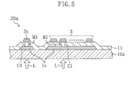
- FIG. 5 is a cross-sectional view of the active matrix substrate 20a, taken along line V-V of FIG. 1 .
- the liquid crystal display apparatus 50a includes the liquid crystal display panel 40a, three film substrates 41 a attached to an upper end of the liquid crystal display panel 40a with an anisotropic conductive film (ACF, not shown) being interposed therebetween, and a printed substrate 45a attached to upper ends of the film substrates 4 1 a with ACF (not shown) being interposed therebetween.
- ACF anisotropic conductive film
- the liquid crystal display panel 40a includes the active matrix substrate 20a and a counter substrate 30 facing each other, and a liquid crystal layer 25 interposed between the active matrix substrate 20a and the counter substrate 30.
- the liquid crystal display panel 40a has a display region D for displaying an image, which is a region where the active matrix substrate 20a and the counter substrate 30 overlap.
- the display region D has three blocks B1-B3 extending in parallel with each other.
- the active matrix substrate 20a includes, in the display region D, a plurality of gate lines 1a (display lines) provided on the insulating substrate 10a and extending in parallel with each other, a plurality of capacitor lines 1b each provided between the corresponding gate lines 1a and extending in parallel with each other, a gate insulating film 11 covering the gate lines 1a and the capacitor lines 1b, a plurality of source lines 3 (display lines) provided on the gate insulating film 11 and extending in parallel with each other in a direction perpendicular to the gate lines 1a (a direction in which the blocks B1-B3 extend), a plurality of thin film transistors (TFT) 5 each provided at an intersection of the corresponding gate line 1a and source line 3, an interlayer insulating film 12 covering the TFTs 5 and the source lines 3, a plurality of pixel electrodes 6 provided in a matrix on the interlayer insulating film 12, and an alignment film (not shown) covering the pixel
- the TFTs 5 each include a gate electrode 1aa protruding laterally from the corresponding gate line 1a, the gate insulating film 11 covering the gate electrode 1 aa, an island-like semiconductor layer 2 on the gate insulating film 11 at a position corresponding to the gate electrode 1aa, and a source electrode 3a and a drain electrode 3b provided on the semiconductor layer 2 and facing each other.
- the source electrode 3a is a laterally protruding portion of the corresponding source line 3.
- the drain electrode 3b is extended to a region overlapping the corresponding capacitor line 1b, thereby forming an auxiliary capacitor, and is also connected to the pixel electrode 6 on the capacitor line 1b via a contact hole 12a formed in the interlayer insulating film 12.
- the active matrix substrate 20a includes, outside the display region D, three on-panel first lines 1c extending along an upper edge of the substrate and intersecting the upper end portions ( FIG. 1 ) of the source lines 3 of the respective blocks B1-B3, three on-panel second line preceding stage portions 3c intersecting left end portions of the respective on-panel first lines 1c, and an L-shaped on-panel second line succeeding stage portion 1d extending along a left edge and a bottom edge of the substrate and intersecting the lower end portions ( FIG. 1 ) of the source lines 3 of all the blocks B1-B3.
- the counter substrate 30 includes an insulating substrate 10b, a black matrix 16 provided on the insulating substrate 10b and having the shape of a frame with a grid therein, a color filter 17 including a red layer, a green layer, and a blue layer, which is provided between each grid bar of the black matrix 16, a common electrode 18 covering the black matrix 16 and the color filter 17, columnar photospacers (not shown) provided on the common electrode 18, and an alignment film (not shown) covering the common electrode 18.
- the liquid crystal layer 25 is formed of, for example, a nematic liquid crystal material having electro-optic properties.
- the film substrates 41a are each, for example, a tape carrier package (TCP). As shown in FIGS. 1 and 2 , the film substrate 41a includes an on-film-substrate first line preceding stage portion 42a connected to a preceding stage portion of the corresponding on-panel first line 1c on the active matrix substrate 20a with ACF (not shown) being interposed therebetween, an on-film-substrate first line succeeding stage portion 42b extending on the left side of and adjacent to the on-film-substrate first line preceding stage portion 42a and connected to a succeeding stage portion of the corresponding on-panel first line 1c on the active matrix substrate 20a with ACF (not shown) being interposed therebetween, an on-film-substrate second line preceding stage portion 43a extending on the left side of and adjacent to the on-film-substrate first line succeeding stage portion 42b and connected to the corresponding on-panel second line preceding stage portion 3c on the active matrix substrate 20a with ACF (not shown) being
- the leftmost film substrate 41a includes an on-film-substrate second line succeeding stage portion 43b connected to the on-panel second line succeeding stage portion 1d on the active matrix substrate 20a with ACF (not shown) being interposed therebetween.
- ACF (not shown) being interposed therebetween.
- the source driver 44a is not shown in the film substrate 41a.
- the printed substrate 45a is, for example, a printed wiring board (PWB). As shown in FIGS. 1 and 2 , the printed substrate 45a includes on-printed-substrate second lines 46a each linking the on-film-substrate second line preceding stage portion 43a on the corresponding film substrate 41a and the on-film-substrate second line succeeding stage portion 43b on the leftmost film substrate 41a with ACF (not shown) being interposed therebetween, and on-printed-substrate first lines 47 each linking the on-film-substrate first line preceding stage portion 42a and the on-film-substrate first line succeeding stage portion 42b on the corresponding film substrate 41a with ACF (not shown) being interposed therebetween.
- PWB printed wiring board
- a first line W1 includes the on-panel first line 1c, the on-film-substrate first line preceding stage portion 42a, the on-printed-substrate first line 47, and the on-film-substrate first line succeeding stage portion 42b.
- a second line W2 includes the on-panel second line preceding stage portion 3c, the on-film-substrate second line preceding stage portion 43a, the on-printed-substrate second line 46a, the on-film-substrate second line succeeding stage portion 43b, and the on-panel second line succeeding stage portion 1d.
- a portion of the first line W1 between an intersection (M3) of the first line W1 and the second line W2 and intersections (M1, etc.) of the first line W1 and the corresponding source lines 3 makes a detour to temporarily pass through a region farther from the display region D.
- liquid crystal display apparatus 50a in each pixel, which is a minimum unit of an image, when a gate signal is transferred from the gate driver via the gate line 1a to the gate electrode 1aa, so that the TFT 5 is turned on, a source signal is transferred from the source driver 44a via the source line 3 to the source electrode 3a, so that predetermined charge is written via the semiconductor layer 2 and the drain electrode 3b to the pixel electrode 6.
- a potential difference occurs between the pixel electrode 6 of the active matrix substrate 20a and the common electrode 18 of the counter substrate 30, whereby predetermined voltage is applied to the liquid crystal layer 25.
- an image is displayed by changing the alignment state of the liquid crystal layer 25 according to the magnitude of the voltage applied to the liquid crystal layer 25 to adjust the light transmittance of the liquid crystal layer 25.
- the manufacturing method of this embodiment includes an active matrix substrate fabrication step, a counter substrate fabrication step, a liquid crystal display panel fabrication step, a broken-line detection step, a broken-line repairing step, a repair confirmation step, and a mounting step.
- a titanium film, an aluminum film, and a titanium film are successively formed on an entirety of the insulating substrate 10a, such as a glass substrate, etc., by sputtering. Thereafter, patterning is performed by photolithography to form the gate lines 1a, the gate electrodes 1aa, the capacitor lines 1b, the on-panel first lines 1c, and the on-panel second line succeeding stage portion 1d, which have a thickness of about 4000 ⁇ .
- a silicon nitride film is formed, by plasma-enhanced chemical vapor deposition (CVD), on an entirety of the substrate on which the gate lines 1a, the gate electrodes 1aa, the capacitor lines 1b, the on-panel first lines 1c, and the on-panel second line succeeding stage portion 1d have been formed, thereby forming the gate insulating film 11 having a thickness of about 4000 ⁇ .
- CVD plasma-enhanced chemical vapor deposition
- an intrinsic amorphous silicon film and a phosphorus-doped n + amorphous silicon film are successively formed, by plasma-enhanced CVD, on an entirety of the substrate on which the gate insulating film 11 has been formed. Thereafter, patterning is performed by photolithography to form an island-like pattern on the gate electrodes 1aa. As a result, a semiconductor layer formation layer is formed in which the intrinsic amorphous silicon layer having a thickness of about 2000 ⁇ and the n + amorphous silicon layer having a thickness of about 500 ⁇ are stacked.
- an aluminum film and a titanium film are formed, by sputtering, on an entirety of the substrate on which the semiconductor layer formation layer has been formed.
- patterning is performed by photolithography to form the source lines 3, the source electrodes 3a, the drain electrodes 3b, and the on-panel second line preceding stage portions 3c, which have a thickness of about 2000 ⁇ .
- the n + amorphous silicon layer of the semiconductor layer formation layer is etched using the source electrodes 3a and the drain electrodes 3b as a mask, i.e., patterning is performed, to form channel portions, thereby forming the semiconductor layer 2 and the TFTs 5 including the semiconductor layer 2.
- a photosensitive acrylic resin is applied, by spin coating, onto an entirety of the substrate on which the TFTs 5 have been formed. Thereafter, the applied photosensitive resin is exposed to light via a photomask and then developed to form the interlayer insulating film 12 having the contact holes 12a on the drain electrodes 3b, which has a thickness of about 2 ⁇ m.
- ITO indium tin oxide
- a polyimide resin is applied, by a printing method, onto an entirety of the substrate on which the pixel electrodes 6 have been formed. Thereafter, a rubbing treatment is performed to form an alignment film having a thickness of about 1000 ⁇ .
- the active matrix substrate 20a can be fabricated.
- a photosensitive acrylic resin in which fine particles made of carbon, etc., are dispersed is applied, by spin coating, onto an entirety of the insulating substrate 10b, such as a glass substrate, etc.
- the applied photosensitive resin is exposed to light via a photomask and then developed to form the black matrix 16 having a thickness of about 1.5 ⁇ m.
- a red, green, or blue colored photosensitive acrylic resin is applied onto the substrate on which the black matrix 16 has been formed.
- the applied photosensitive resin is exposed to light via a photomask, followed by development (i.e., patterning is performed), to form a colored layer having a selected color (e.g., a red layer) having a thickness of about 2.0 ⁇ m.
- a similar process is repeated to form colored layers having the other colors (e.g., a green layer and a blue layer) having a thickness of about 2.0 ⁇ m.
- the color filter 17 is formed.
- an ITO film is formed, by sputtering, on the substrate on which the color filter 17 has been formed, to form the common electrode 18 having a thickness of about 1500 ⁇ .
- a photosensitive phenol novolac resin is applied, by spin coating, onto an entirety of the substrate on which the common electrode 18 has been formed.
- the applied photosensitive resin is exposed to light via a photomask and then developed to form photospacers having a thickness of about 4 ⁇ m.
- a polyimide resin is applied, by printing, on an entirety of the substrate on which the photospacers have been formed. Thereafter, a rubbing treatment is performed to form an alignment film having a thickness of about 1000 ⁇ .
- the counter substrate 30 can be fabricated.
- a sealing material made of an ultraviolet and thermal curing resin is applied (drawn) in the shape of a frame, using a dispenser, onto the counter substrate 30 which has been fabricated in the counter substrate fabrication step.
- a liquid crystal material is dropped into a region inside the sealing material of the counter substrate 30 on which the sealing material has been applied.
- the counter substrate 30 on which the liquid crystal material has been dropped and the active matrix substrate 20a which has been fabricated in the active matrix substrate fabrication step are joined with each other under reduced pressure. Thereafter, the joined substrates are exposed to the atmosphere so that pressure is applied on the outer surfaces of the joined substrates.
- the sealing material interposed between the joined substrates is irradiated with ultraviolet (UV) light and then heated so that the sealing material is cured.
- UV ultraviolet
- the liquid crystal display panel 40a can be fabricated. Thereafter, a polarizing plate is attached to each of the front and back surfaces of the liquid crystal display panel 40a.
- the polarizing plate may be attached before the broken-line detection step or in the mounting step described below.
- the polarizing plate is attached to each of the front and back surfaces of the liquid crystal display panel 40a in which a broken line has not been detected in the broken-line detection step or in which a broken line has been repaired in the broken-line repairing step and the repair confirmation step.
- the broken-line detection step described below is performed with respect to the liquid crystal display panel 40a thus fabricated.
- the break is repaired by the broken-line repairing step, and thereafter, a connection state between the repaired source line 3 and other lines is confirmed by the repair confirmation step.
- a gate test signal which is a +15-V pulse voltage having a bias voltage of -10 V, a period of 16.7 msec, and a pulse width of 50 ⁇ sec is input to each gate line 1a so that all the TFTs 5 are turned on.
- a source test signal having a potential of ⁇ 2 V whose polarity is reversed every 16.7 msec is input to each source line 3 so that an amount of charge corresponding to ⁇ 2 V is written via the source electrode 3a and the drain electrode 3b of each TFT 5 to the pixel electrode 6.
- a common electrode test signal which is a direct current having a potential of -1 V is input to the common electrode 18.
- a voltage is applied to a liquid crystal capacitor formed between the pixel electrode 6 and the common electrode 18, so that a pixel formed by the pixel electrode 6 is turned on, i.e., white display is changed to black display in the case of the normally white mode (white display is obtained in the absence of voltage application).
- white display is changed to black display in the case of the normally white mode (white display is obtained in the absence of voltage application).
- a light source is provided at the back of the liquid crystal display panel 40a, the display state can be visually confirmed.
- a polarizing plate is placed at the front of the liquid crystal display panel 40a, and a polarizing plate is provided between the liquid crystal display panel 40a and a light source, to confirm the display state.
- a pixel on a source line 3 having a break For a pixel on a source line 3 having a break, a predetermined amount of charge cannot be written to the pixel electrode 6, and therefore, the pixel is not turned on (bright spot), whereby a break portion (portion X) of the source line 3 is detected.
- an intersection M1 of the source line 3 on which a break has been detected at the portion X in the broken-line detection step and the corresponding first line W1 (the on-panel first line 1c), an intersection M2 of that source line 3 and the second line W2 (the on-panel second line succeeding stage portion 1d), and an intersection M3 of the corresponding first line W1 (the on-panel first line 1c) and the second line W2 (the on-panel second line preceding stage portion 3c) are irradiated with laser light L emitted by a YAG laser, etc., through the insulating substrate 10a.
- contact holes C1-C3 (C2 is not shown) are formed in the gate insulating film 11 at the intersections M1-M3 so that the metal layers forming the lines are fused.
- conduction is established between an upper portion ( FIG. 1 ) of the broken source line 3 and the corresponding first line W1, between a lower portion ( FIG. 1 ) of the broken source line 3 and the second line W2, and between the corresponding first line W1 and the second line W2.
- an electrical resistance between the first terminal T1 connected to the repaired source line 3 and the third terminal T3, and an electrical resistance between the second terminal T2 and the fourth terminal T4, are measured to confirm a connection state between the repaired source line 3 and the corresponding first line W1 and a connection state between the corresponding first line W1 and the second line W2. Note that if a faulty connection state has been confirmed, the intersection for which the fault has been confirmed is irradiated with laser light again (the connection is reworked) so that conduction between the lines is ensured.
- the three film substrates 41a are previously attached to the printed substrate 45a with ACF being interposed therebetween.
- the film substrates 41a are attached to the liquid crystal display panel 40a in which a broken line has not been detected in the broken-line detection step or the liquid crystal display panel 40a in which a broken line has been repaired in the broken-line repairing step and the repair confirmation step, with ACF being interposed therebetween.
- liquid crystal display apparatus 50a of this embodiment can be fabricated.
- the first lines W1 and the second line W2 are provided outside the display region D including the blocks B1-B3 extending in parallel with each other. Also, the first lines W1 intersecting end portions closer to the source drivers 44a of the source lines 3 extending in parallel with each other in the blocks B1-B3 (the first lines W1 and the source lines 3 are insulated from each other) intersect the second line W2 intersecting end portions farther from the source drivers 44a of the source lines 3 in all the blocks B1-B3 (the second line W2 and the source lines 3 are insulated from each other), where the first and second lines W1 and W2 are insulated from each other.
- intersections (M1, etc.) of the first lines W 1 and the source lines 3 in the respective blocks B1-B3, intersections (M2, etc.) of the second line W2 and the source lines 3 in all the blocks B1-B3, and the intersections (M3, etc.) of the first lines W1 and the second line W2 are provided outside the display region D of the liquid crystal display panel 40a. Therefore, a broken source line 3 can be easily repaired as follows. Specifically, if any one of all the source lines 3 provided on the liquid crystal display panel 40a is broken at a portion X, the broken line is detected in the broken-line detection step, and the broken line is repaired in the broken-line repairing step.
- an intersection M1 of a portion closer to the source driver 44a of the broken source line 3 and the corresponding first line W1, an intersection M2 of a portion farther from the source driver 44a of the broken source line 3 and the second line W2, and an intersection M3 of the corresponding first line W1 and the second line W2, i.e., only three portions of the liquid crystal display panel 40a, are irradiated with laser light L to establish conduction between each line.
- the amplifier circuit A is provided for each first line W1, i.e., for each of the blocks B1-B3. Therefore, conduction is established between each line as described above while reducing or preventing a difference between signal delays depending on the positions of the blocks B1-B3 where a break occurs.
- a source signal from the source driver 44a is amplified by the amplifier circuit A and then supplied to a portion farther than the break portion of the broken source line 3.
- the liquid crystal display panel 40a is the only target to be irradiated with the laser light L, and therefore, conditions for irradiation with the laser light L are simplified, whereby the broken source line 3 can be easily repaired.
- the first terminals T1 connected to the source lines 3, the second terminal T2 connected to the second line W2, and the third terminal T3 and the fourth terminal T4 connected to the preceding stage portion (42a) closer to the first terminals T1 and the succeeding stage portion (42b) closer to the second terminal T2 on the detour path of the first line W1, respectively, are provided.
- an electrical resistance between the first terminal T1 connected to the repaired source line 3 and the third terminal T3, and an electrical resistance between the second terminal T2 and the fourth terminal T4, are measured to confirm a connection state between the repaired source line 3 and the first line W1 and a connection state between the first line W1 and the second line W2, whereby a faulty connection portion can be easily identified.
- repairing of a broken line can be correctly reworked, thereby hindering or preventing a defective product in which a broken line has not been correctly repaired from being supplied to the next step.
- the liquid crystal display apparatus 50a of this embodiment and the manufacturing method therefor in the blocks B1 and B3 other than the block B2 in which a broken line has been repaired, the first line W1 intersecting the source lines 3 is not connected to the second line W2, and therefore, the load of the second line W2 can be reduced. In other words, the signal delay of a repaired line can be reduced, and therefore, the success of repairing can be more reliably achieved.
- the first lines may be each a plurality of lines intersecting each other with an insulating film being interposed therebetween (the lines overlap).
- the lines overlap When a broken line is repaired, an intersection (overlap) between lines is irradiated with laser light to link the lines, thereby forming the first line.
- the second line may be each a plurality of lines intersecting each other with an insulating film being interposed therebetween (the lines overlap).
- an intersection (overlap) of lines is irradiated with laser light to link the lines, thereby forming the second line.
- the film substrates 41 a do not need to be all identical substrates.
- the film substrates 41a are, however, preferably all identical substrates in terms of cost reduction caused by volume production, manufacture management, etc.
- FIG. 6 is an enlarged plan view of a film substrate 41b included in a liquid crystal display apparatus 50b according to this embodiment and a surrounding configuration thereof. Note that the same parts as those of FIGS. 1-5 are indicated by the same reference characters in embodiments described below.
- first line W1 and a single amplifier circuit A are provided for each film substrate 41a in the first embodiment
- two first lines W1 and two amplifier circuits A are provided for each film substrate 41b in this embodiment as shown in FIG. 6 .
- the liquid crystal display apparatus 50b of this embodiment includes an active matrix substrate 20b (liquid crystal display panel 40b) which includes a plurality of source lines 3.
- the source lines 3 are divided into blocks B1-B3.
- Each block includes two line groups G1 and G2 each including a plurality of source lines 3.
- a first line W1 and an amplifier circuit A are provided for each of the line groups G1 and G2.
- the liquid crystal display panel 40b is the only target to be irradiated with laser light L to repair a broken line. Therefore, a broken source line 3 can be easily repaired.
- a first line W1 and an amplifier circuit A are provided for each of the line groups G1 and G2, and therefore, a difference between signal delays depending on the positions of the blocks B1-B3 where a break occurs can be further reduced or prevented.
- the load of a source line 3 in which a break has been repaired can be reduced, whereby a fault in display caused by a signal delay or other influences of a source signal can be reduced.
- FIG. 7 is a plan view of a liquid crystal display apparatus 50c according to this embodiment.
- a source driver 35a is provided on a liquid crystal display panel 40c (active matrix substrate 20c) in this embodiment.
- the liquid crystal display apparatus 50c includes the liquid crystal display panel 40c, and a film substrate 45c attached to an upper end of the liquid crystal display panel 40c with ACF (not shown) being interposed therebetween.
- the liquid crystal display panel 40c includes the active matrix substrate 20c and a counter substrate 30 facing each other.
- the active matrix substrate 20c has a display region D having substantially the same configuration as that of the active matrix substrate 20a of the first embodiment. As shown in FIG. 7 , the active matrix substrate 20c includes, outside the display region D, three on-panel first lines 1cc extending along an upper edge of the substrate and intersecting upper end portions of source lines 3 provided in respective blocks B1-B3, three on-panel second line preceding stage portions 3cc intersecting left end portions of the respective on-panel first lines 1cc, an L-shaped on-panel second line succeeding stage portion 1dc extending along a left edge and a bottom edge of the substrate and intersecting lower end portions of the source lines 3 of all the blocks B1-B3, and the source drivers 35a (drive circuits) provided in the respective blocks B1-B3 and connected to the source lines 3 of the respective blocks B1-B3.
- the source drivers 35a drive circuits
- the film substrates 45c are each, for example, a flexible printed circuit (FPC), etc. As shown in FIG. 7 , the film substrate 45c includes an on-film-substrate second line 46c linking the on-panel second line preceding stage portions 3cc on the active matrix substrate 20c and the on-panel second line succeeding stage portion 1dc with ACF (not shown) being interposed therebetween.
- FPC flexible printed circuit
- the second line W2 includes the on-panel second line preceding stage portions 3cc, the on-film-substrate second line 46c, and the on-panel second line succeeding stage portion 1dc.
- a portion of the first line 1cc (W1) between an intersection (M3) of the first line 1cc and the second line W2 and intersections (M1, etc.) of the first line 1cc and the corresponding source lines 3 makes a detour to temporarily pass through a region farther from the display region D.
- the liquid crystal display apparatus 50c having the above configuration can be manufactured by changing the line patterns in the method of fabricating the active matrix substrate 20a of the first embodiment and mounting the source drivers 35a and the film substrate 45c thereonto.
- the liquid crystal display panel 40c is the only target to be irradiated with laser light L to repair a broken line. Therefore, a broken source line 3 can be easily repaired.
- FIG. 8 is a plan view of a liquid crystal display apparatus 50d according to this embodiment.
- the entire second line W2 is provided on a liquid crystal display panel 40d (active matrix substrate 20d) in this embodiment.
- the liquid crystal display apparatus 50d i.e., the liquid crystal display panel 40d, includes an active matrix substrate 20d and a counter substrate 30 facing each other.
- the active matrix substrate 20d has a display region D having substantially the same configuration as that of the active matrix substrate 20a of the first embodiment. As shown in FIG. 8 , the active matrix substrate 20d includes, outside the display region D, three L-shaped first lines 1cd (W1) extending along an upper edge of the substrate and intersecting upper end portions of source lines 3 provided in respective blocks B1-B3, an L-shaped second line 1dd (W2) extending along a left edge and a lower edge of the substrate and intersecting lower end portions of the source lines 3 of all the blocks B1-B3, and source drivers 35b (drive circuits) provided in the respective blocks B1-B3 and connected to the source lines 3 of the respective blocks B1-B3.
- W1 first lines 1cd
- W2 L-shaped second line 1dd
- the liquid crystal display apparatus 50d having the above configuration can be manufactured by changing the line patterns in the method of fabricating the active matrix substrate 20a of the first embodiment and mounting the source drivers 35b thereonto.
- the liquid crystal display panel 40d is the only target to be irradiated with laser light L to repair a broken line. Therefore, a broken source line 3 can be easily repaired.
- FIG. 9 is a plan view of a liquid crystal display apparatus 50e according to this embodiment.
- a source line 3 is described as an example display line in which a break is repaired in the first to fourth embodiments
- a gate line 1a is described as an example display line in which a break is repaired in this embodiment.
- the liquid crystal display apparatus 50e includes a liquid crystal display panel 40e, three film substrates 41b attached to an upper end portion of the liquid crystal display panel 40e with ACF (not shown) being interposed therebetween, and a printed substrate 45a attached to upper ends of the film substrates 41b with ACF (not shown) being interposed therebetween.
- the liquid crystal display panel 40e includes an active matrix substrate 20e and a counter substrate 30 facing each other.
- the active matrix substrate 20e has a display region D having substantially the same configuration as that of the active matrix substrate 20a of the first embodiment, except that the vertical and horizontal directions are switched. As shown in FIG. 9 , the active matrix substrate 20e includes, outside the display region D, three on-panel first lines 3dc extending along an upper edge of the substrate and intersecting upper end portions of gate lines 1a provided in respective blocks B1-B3, three on-panel second line preceding stage portions 3ce intersecting left end portions of the respective on-panel first lines 3dc, and an L-shaped on-panel second line succeeding stage portion 3dd extending along a left edge and a bottom edge of the substrate and intersecting lower end portions of the gate lines 1a of all the blocks B1-B3.
- the on-panel first lines 3dc, the on-panel second line preceding stage portion 3ce, and the on-panel second line succeeding stage portion 3dd are formed of the same material and in the same layer as those of the source lines 3.
- the film substrates 41b are each, for example, TCP.
- the film substrate 41b includes an on-film-substrate first line preceding stage portion 42a connected to a preceding stage portion of the corresponding on-panel first line 3dc on the active matrix substrate 20a with ACF (not shown) being interposed therebetween, an on-film-substrate first line succeeding stage portion 42b extending on the left side of and adjacent to the on-film-substrate first line preceding stage portion 42a and connected to a succeeding stage portion of the corresponding on-panel first line 3dc on the active matrix substrate 20a with ACF (not shown) being interposed therebetween, an on-film-substrate second line preceding stage portion 43a extending on the left side of and adjacent to the on-film-substrate first line succeeding stage portion 42b and connected to the corresponding on-panel second line preceding stage portion 3ce on the active matrix substrate 20a with ACF (not shown) being interposed therebetween, a gate
- the printed substrate 45a is, for example, PWB. As shown in FIG. 9 , the printed substrate 45a includes on-printed-substrate second lines 46a each linking the on-film-substrate second line preceding stage portion 43a on the corresponding film substrate 41a and the on-film-substrate second line succeeding stage portion 43b on the leftmost film substrate 41a with ACF (not shown) being interposed therebetween, and on-printed-substrate first lines 47 each linking the on-film-substrate first line preceding stage portion 42a and the on-film-substrate first line succeeding stage portion 42b on the corresponding film substrate 41a with ACF (not shown) being interposed therebetween.
- on-printed-substrate second lines 46a each linking the on-film-substrate second line preceding stage portion 43a on the corresponding film substrate 41a and the on-film-substrate second line succeeding stage portion 43b on the leftmost film substrate 41a with ACF (not shown) being interposed there
- a first line W1 includes the on-panel first line 3dc, the on-film-substrate first line preceding stage portion 42a, the on-printed-substrate first line 47, and the on-film-substrate first line succeeding stage portion 42b.
- a second line W2 includes the on-panel second line preceding stage portion 3ce, the on-film-substrate second line preceding stage portion 43a, the on-printed-substrate second line 46a, the on-film-substrate second line succeeding stage portion 43b, and the on-panel second line succeeding stage portion 3dd.
- the liquid crystal display apparatus 50e having the above configuration can be manufactured by changing the line patterns in the method of fabricating the active matrix substrate 20a of the first embodiment.
- the first lines W1 and the second line W2 are provided outside the display region D including a plurality of blocks B1-B3 extending in parallel with each other. Also, the first lines W1 intersecting end portions closer to the gate drivers 44b of the gate lines 1a extending in parallel with each other in the blocks B1-B3 (the first lines W1 and the gate lines 1a are insulated from each other) intersect the second line W2 intersecting end portions farther from the gate drivers 44b of the gate lines 1a in all the blocks B1-B3 (the second line W2 and the gate lines 1a are insulated from each other), where the first and second lines W1 and W2 are insulated from each other.
- intersections (M1, etc.) of the first lines W1 and the gate lines 1a in the respective blocks B1-B3, intersections (M2, etc.) of the second line W2 and the gate lines 1a in all the blocks B1-B3, and intersections (M3, etc.) of the first lines W1 and the second line W2 are provided outside the display region D of the liquid crystal display panel 40e. Therefore, a broken gate line 1a can be easily repaired as follows. Specifically, if any one of all the gate lines 1a provided on the liquid crystal display panel 40e is broken at a portion X, the broken line is detected in the broken-line detection step, and the broken line is repaired in the broken-line repairing step.
- an intersection M1 of a portion closer to the gate driver 44b of the broken gate line 1a and the corresponding first line W1, an intersection M2 of a portion farther from the source driver 44b of the broken gate line 1a and the second line W2, and an intersection M3 of the corresponding first line W1 and the second line W2, i.e., only three portions of the liquid crystal display panel 40e, are irradiated with laser light L to establish conduction between each line.
- the amplifier circuit A is provided for each first line W1, i.e., for each of the blocks B1-B3. Therefore, conduction is established between each line as described above while reducing or preventing a difference between signal delays depending on the positions of the blocks B1-B3 where a break occurs.
- a gate signal from the gate driver 44b is amplified by the amplifier circuit A and then supplied to a portion farther than the break portion of the broken gate line 1a.
- the liquid crystal display panel 40e is the only target to be irradiated with the laser light L, and therefore, conditions for irradiation with the laser light L are simplified, whereby the broken gate line 1a can be easily repaired.
- FIG. 10 is a plan view of an active matrix substrate 20f according to this embodiment.
- a liquid crystal display apparatus may be constructed by interposing and enclosing a liquid crystal layer between the active matrix substrate 20f of this embodiment and a counter substrate.
- a sensor substrate which reads charge on each pixel electrode, such as an X-ray sensor, etc., may be provided using the active matrix substrate 20f. Note that, in the latter case, a liquid crystal layer and a counter substrate for enclosing a liquid crystal layer are not required.
- the active matrix substrate 20f has substantially the same configuration as that of the active matrix substrate 20d of the fourth embodiment.
- a break in a display line (e.g., a source line 3) is detected in the active matrix substrate 20f by the follow methods: conduction is tested for each line by contacting probes to opposite end portions of the line; a portion having an abnormal pattern of the display region D is detected by image recognition, and a break portion is extracted from the detected abnormal portion; an amount of charge similar to that in actual operation is written to all pixels, and after a predetermined time has elapsed, the written charge is read out, and based on a change in the charge, it is determined whether the pixel is good or defective; etc.
- conduction is tested for each line by contacting probes to opposite end portions of the line
- a portion having an abnormal pattern of the display region D is detected by image recognition, and a break portion is extracted from the detected abnormal portion
- an amount of charge similar to that in actual operation is written to all pixels, and after a predetermined time has elapsed, the written charge is read out, and based on a change in the charge, it is determined whether the
- the broken source line 3 can be repaired by irradiating an intersection M1 of the detected broken source line 3 and a corresponding first line 1cd, an intersection M2 of the broken source line 3 and a second line 1dd, and an intersection M3 of the first line 1cd and the second line 1dd with laser light L to establish conduction between each line in the intersections M1-M3.
- the first lines 1cd and the second line 1dd are provided outside the display region D including a plurality of blocks B1-B3 extending in parallel with each other. Also, the first lines 1cd intersecting end portions closer to source drivers 35b of the source lines 3 extending in parallel with each other in the respective blocks B1-B3 (the first lines 1cd and the source lines 3 are insulated from each other) intersect the second line 1dd intersecting end portions farther from the source drivers 35b of the source lines 3 in all the blocks B1-B3 (the second line 1dd and the source lines 3 are insulated from each other), where the first and second lines 1cd and 1dd are insulated from each other.
- intersections (M1, etc.) of the first lines 1cd and the source lines 3 in the respective blocks B1-B3, intersections (M2, etc.) of the second line 1dd and the source lines 3 in all the blocks B1-B3, and intersections (M3, etc.) of the first lines 1cd and the second line 1dd are provided outside the display region D of the active matrix substrate 20f. Therefore, a broken source line 3 can be easily repaired as follows. Specifically, if any one of all the source lines 3 provided on the active matrix substrate 20f is broken at a portion X, the broken line is detected in the broken-line detection step, and the broken line is repaired in the broken-line repairing step.
- an intersection M1 of a portion closer to the source driver 35b of the broken source line 3 and the corresponding first line 1cd, an intersection M2 of a portion farther from the source driver 35b of the broken source line 3 and the second line 1dd, and an intersection M3 of the corresponding first line 1cd and the second line 1dd, i.e., only three portions of the active matrix substrate 20f, are irradiated with laser light L to establish conduction between each line.
- an amplifier circuit A is provided for each first line 1cd, i.e., for each of the blocks B1-B3.
- a liquid crystal display apparatus has been described as an example display apparatus, the present disclosure is applicable to other display apparatuses, such as an organic electroluminescent (EL) display apparatus, a field emission display (FED), etc.
- EL organic electroluminescent
- FED field emission display
- the present disclosure is applicable to repairing of a short circuit between a gate line and a source line. Specifically, when there is a short circuit between a gate line and a source line, a portion of the gate or source line including the short circuit is cut by, for example, irradiation with laser light so that the gate or source line has a break. Thereafter, the broken gate or source line is repaired as in the above embodiments.
- liquid crystal display apparatus 50a of the first embodiment in which a broken source line 3 can be repaired may be combined with the liquid crystal display apparatus 50e of the fifth embodiment in which a broken gate line 1a can be repaired.
- the entire second line W2 is provided on a liquid crystal display panel (an active matrix substrate), a portion of the second line W2 may be provided on an external substrate attached to the liquid crystal display panel.
- the first and second lines may have a spare capacitor for adjusting a signal waveform which can be connected thereto by irradiation with laser light.
- a broken display line can be efficiently repaired using a simple line configuration, thereby reducing the manufacturing cost of a display apparatus.
- the present disclosure is particularly useful for a high-definition display apparatus having a large number of lines, a display apparatus designed to have a narrow frame region around a display region, etc.
Landscapes
- Physics & Mathematics (AREA)
- Engineering & Computer Science (AREA)
- General Physics & Mathematics (AREA)
- Computer Hardware Design (AREA)
- Chemical & Material Sciences (AREA)
- Crystallography & Structural Chemistry (AREA)
- Nonlinear Science (AREA)
- Theoretical Computer Science (AREA)
- Mathematical Physics (AREA)
- Optics & Photonics (AREA)
- Microelectronics & Electronic Packaging (AREA)
- Devices For Indicating Variable Information By Combining Individual Elements (AREA)
- Liquid Crystal (AREA)
- Control Of Indicators Other Than Cathode Ray Tubes (AREA)
- Liquid Crystal Display Device Control (AREA)
Abstract
Description
- The present disclosure relates to display apparatuses and methods for manufacturing the display apparatuses, and active matrix substrates. More particularly, the present disclosure relates to techniques of repairing a break in a line for display provided in an active matrix substrate and a display apparatus.
- A liquid crystal display apparatus includes, for example, an active matrix substrate and a counter substrate facing each other. The active matrix substrate includes, for example, lines for display (hereinafter referred to as display lines) including a plurality of gate lines extending in parallel with each other and a plurality of source lines extending in parallel with each other and in a direction perpendicular to the gate lines. Therefore, the liquid crystal display apparatus including the active matrix substrate has the following problem. If a break occurs in a display line, such as a gate line or a source line, a display signal is not supplied from a drive circuit to a portion farther than the break of the broken display line, resulting in a significant degradation in display quality.
- In order to solve the above problem, a variety of liquid crystal display apparatuses have been proposed which include lines for repairing a broken line and amplifier circuits connected to the broken-line repairing lines, which are provided outside a display region for displaying an image (see, for example, Japanese Patent Publication Nos.
2000-321599 H11-160677 2000-105576 2008-58337 -
FIG. 11 is a plan view of a conventional liquidcrystal display apparatus 150 corresponding to the plan view described in Japanese Patent Publication No.2000-321599 figure 5 ), schematically showing a liquid crystal display element and drive circuit substrates provided around the element. - As shown in
FIG. 11 , the liquidcrystal display apparatus 150 includes a liquidcrystal display panel 140, threefilm substrates 141 attached to an upper end of the liquidcrystal display panel 140, and a printedsubstrate 145 attached to upper ends of thefilm substrates 141. - As shown in
FIG. 11 , the liquidcrystal display panel 140 includes, in a display region D, a plurality ofsource lines 103 extending in parallel with each other and a plurality of gate lines (not shown) extending in parallel with each other and in a direction perpendicular to thesource lines 103. Here, as shown inFIG. 11 , thesource lines 103 are divided into blocks B1-B3 which are adjacent to each other and each include a plurality of thesource lines 103. Thesource lines 103 in the respective blocks B1-B3 are each connected to a drive circuit (not shown) provided on thecorresponding film substrate 141. - As shown in
FIG. 11 , the liquidcrystal display panel 140 includes, outside the display region D, three on-panelfirst lines 101 c extending along an upper side of the display region D and intersecting upper end portions of thesource lines 103 provided in the respective blocks B1-B3, and an L-shaped on-panelsecond line 101d extending along a left side and a bottom side of the display region D and intersecting lower end portions of thesource lines 103. - As shown in
FIG. 11 , the printedsubstrate 145 includes three on-printed-substratefirst lines 146 connected to the on-panelfirst lines 101c via on-film-substratefirst lines 142 provided on thefilm substrates 141, respectively, an on-printed-substratesecond line 147 intersecting upper end portions of the on-printed-substratefirst lines 146 and connected to the on-panelsecond line 101d via an on-film-substratesecond line 143 provided on theleftmost film substrate 141, and an amplifier circuit A provided in a left end portion of the on-printed-substratesecond line 147. - It is assumed that, as shown in
FIG. 11 , in the liquidcrystal display apparatus 150 thus configured, when asource line 103 in the block B2 is broken at a portion X. In this case, an intersection M1 of an upper portion of thebroken source line 103 and the on-panelfirst line 101c of the block B2, an intersection M2 of a lower portion of thebroken source line 103 and the on-panelsecond line 101d, and an intersection M3 of the on-printed-substratefirst line 146 of the block B2 and the on-printed-substratesecond line 147 are irradiated with laser light. As a result, conduction is established between the upper portion of thebroken source line 103 and the on-panelfirst line 101c of the block B2, between the lower portion of thebroken source line 103 and the on-panelsecond line 101d, and between the on-printed-substratefirst line 146 of the block B2 and the on-printed-substratesecond line 147. As a result, as shown inFIG. 11 , a display signal (source signal) is supplied from the drive circuit (not shown) provided on thefilm substrate 141 to a portion lower than the portion X of thesource line 103 via the on-panelfirst line 101c of the block B2, the on-film-substratefirst line 142 of the block B2, the on-printed-substratefirst line 146 of the block B2, the on-printed-substratesecond line 147, the amplifier circuit A, the on-film-substratesecond line 143, and the on-panelsecond line 101d. Therefore, the source signal is supplied from the drive circuit to a portion farther than the break portion (the portion X) of thesource line 103, whereby the break in thesource line 103 can be repaired. - As described above, the
broken source line 103 is repaired in the liquidcrystal display apparatus 150 by, for example, irradiating the intersections M1-M3 with laser light to establish conduction between each line. In this case, however, the intersections M1-M3 are provided on both the liquidcrystal display panel 140 and the printedsubstrate 145, and therefore, a plurality of laser irradiation devices are required and conditions for irradiation with laser light are complicated, leading to an increase in manufacturing cost. Therefore, there is a room for improvement. - The present disclosure has been made in view of the above problem. The detailed description describes implementations of a technique of easily repairing a break in a display line.
- According to the present disclosure, first lines inserting end portions closer to drive circuits of display lines in respective blocks and insulated from the display lines, intersect a second line inserting end portions farther than the drive circuits of the display lines in all the blocks on a display panel and insulated from the display lines, where the first lines are insulated from the second line.
- Specifically, an example display apparatus of the present disclosure includes a display panel having a display region including a plurality of blocks extending in parallel with each other. The display panel includes a plurality of display lines provided in each of the blocks and extending in parallel with each other and in a direction in which the blocks extend, a plurality of drive circuits each provided outside the display region for a corresponding one of the blocks and connected to the display lines in the corresponding block, a plurality of first lines each provided outside the display region for a corresponding one of the blocks and intersecting end portions closer to the corresponding drive circuit of the display lines in the corresponding block, the first lines being insulated from the display lines, and a second line provided outside the display region and intersecting end portions farther from the drive circuits of the display lines of all the blocks, the second line being insulated from the display lines. The second line is configured to intersect the first lines while being insulated from the first lines, and be supplied with a display signal from each of the drive circuits via an amplifier circuit.
- In the above configuration, outside the display region including the blocks extending in parallel with each other, the first lines inserting the end portions closer to the drive circuits of the display lines extending in parallel with each other in the respective blocks, the first lines being insulated from the display lines, intersect the second line inserting the end portions farther than the drive circuits of the display lines in all the blocks, the second line being insulated from the display lines, where the first lines are insulated from the second line. Therefore, intersections of the first lines and the display lines in the respective blocks, intersections of the second line and the display lines in all the blocks, and intersections of the first lines and the second line are provided outside the display region of the display panel. Therefore, a broken display line can be repaired as follows. Specifically, if any one of all the display lines provided on the display panel is broken, an intersection of a portion closer to the driver circuit of the broken display line and the corresponding first line, an intersection of a portion farther from the driver circuit of the broken display line and the second line, and an intersection of the corresponding first line and the second line, i.e., only three portions of the display panel, are irradiated with laser light to establish conduction between each line. In addition, the second line is configured to be supplied with a display signal from each drive circuit via an amplifier circuit. Therefore, by establishing conduction between each line in the above-described manner, a display signal from a drive circuit is amplified by an amplifier circuit and then supplied to a portion farther than a break portion of a broken display line. As a result, when a broken display line is repaired, the display panel is the only target to be irradiated with laser light, and therefore, conditions for irradiation with the laser light are simplified, whereby the broken display line can be easily repaired.
- For example, Japanese Patent Publication No.
2000-321599 FIG. 1 ) describes a technique of irradiating two points on a display panel with laser light to establish conduction between each line. In this case, a single line corresponding to the first line is provided for all blocks. Loads occur at capacitances at intersections of the line corresponding to the first line and a plurality of signal lines in all the blocks, likely leading to an increase in signal delay. In contrast to this, in the above configuration, the first line is provided for each block, and therefore, the signal delay can be reduced or prevented. - The amplifier circuit may be provided in a portion of each of the first lines between an intersection of the first line and the second line and intersections of the first line and the corresponding display lines.
- According to the above configuration, the amplifier circuit is provided for each first line, i.e., for each block, and therefore, a difference between signal delays depending on the position of a block in which a break occurs can be reduced or prevented.
- Another example display apparatus of the present disclosure includes a display panel having a display region including a plurality of blocks extending in parallel with each other. The display panel includes a plurality of display lines provided in each of the blocks and extending in parallel with each other and in a direction in which the blocks extend, a plurality of drive circuits each provided outside the display region for a corresponding one of the blocks and connected to the display lines in the corresponding block, a plurality of first lines each provided outside the display region for a corresponding one of the blocks and intersecting end portions closer to the corresponding drive circuit of the display lines in the corresponding block, the first lines being insulated from the display lines, and a second line provided outside the display region and intersecting end portions farther from the drive circuits of the display lines of all the blocks, the second line being insulated from the display lines. The second line is configured to intersect the first lines while being insulated from the first lines, and an amplifier circuit is provided in each of the first lines.
- In the above configuration, outside the display region including the blocks extending in parallel with each other, the first lines inserting the end portions closer to the drive circuits of the display lines extending in parallel with each other in the respective blocks, the first lines being insulated from the display lines, intersect the second line inserting the end portions farther than the drive circuits of the display lines in all the blocks, the second line being insulated from the display lines, where the first lines are insulated from the second line. Therefore, intersections of the first lines and the display lines in the respective blocks, intersections of the second line and the display lines in all the blocks, and intersections of the first lines and the second line are provided outside the display region of the display panel. Therefore, a broken display line can be repaired as follows. Specifically, if any one of all the display lines provided on the display panel is broken, an intersection of a portion closer to the driver circuit of the broken display line and the corresponding first line, an intersection of a portion farther from the driver circuit of the broken display line and the second line, and an intersection of the corresponding first line and the second line, i.e., only three portions of the display panel, are irradiated with laser light to establish conduction between each line. In addition, the amplifier circuit is provided in each first line. Therefore, by establishing conduction between each line in the above-described manner, a display signal from a drive circuit is amplified by an amplifier circuit and then supplied to a portion farther than a break portion of a broken display line. As a result, when a broken display line is repaired, the display panel is the only target to be irradiated with laser light, and therefore, conditions for irradiation with the laser light are simplified, whereby the broken display line can be easily repaired.
- A portion of each of the first lines between an intersection of the first line and the second line and intersections of the first line and the corresponding display lines may make a detour to temporarily pass through a region farther from the display region.
- In the above configuration, a portion of each of the first lines between an intersection of the first line and the second line and intersections of the first line and the corresponding display lines makes a detour. Therefore, in a block in which a broken display line has been repaired, by measuring electrical resistances between the detour portion of the first line, and the display line in which a break has been repaired and the second line, a connection state between the display line in which a break has been repaired and the first line, and a connection state between the first line and the second line can be confirmed.
- The display apparatus may include, for each of the blocks, a plurality of first terminals connected to the respective display lines, a second terminal connected to the second line, a third terminal connected to a preceding stage portion closer to the plurality of first terminals of a detour path of the corresponding first line, and a fourth terminal connected to a succeeding stage portion closer to the second terminal of the detour path of the corresponding first line, the first to fourth terminals being provided outside the display region.
- In the above configuration, the first terminals connected to the respective display lines, the second terminal connected to the second line, the third terminal connected to the preceding stage portion closer to the first terminals of the detour path of the corresponding first line, and the fourth terminal connected to the succeeding stage portion closer to the second terminal of the detour path of the corresponding first line, are provided for each block. In a block in which a broken display line has been repaired, by measuring an electrical resistance between the first terminal connected to the repaired display line and the third terminal, and an electrical resistance between the second terminal and the fourth terminal, a connection state between the repaired display line and the corresponding first line and a connection state between the corresponding first line and the second line can be confirmed.
- The display apparatus may further include a plurality of film substrates each provided for a corresponding one of the blocks and attached to an end portion outside the display region of the display panel. The detour paths of the first lines may be provided on the respective film substrates. The first, second, third, and fourth terminals may be provided on each of the film substrates. The amplifier circuit may be incorporated in the drive circuit provided in each of the film substrates.
- In the above configuration, for a block in which a broken display line has been repaired, by measuring an electrical resistance between one of the first terminals (connected to the repaired display line) provided on the film substrate including a drive circuit including an amplifier circuit, and the third terminal, and an electrical resistance between the second terminal and the fourth terminal, a connection state between the repaired display line and the first line, and a connection state between the first line and the second line, can be confirmed. Therefore, an advantage of the present disclosure is specifically achieved.
- The display apparatus may include a printed substrate attached to end portions farther from the display panel of the film substrates. On the printed substrate, lines each linking the preceding stage portion and the succeeding stage portion of the detour path of the corresponding first line may be provided.
- In the above configuration, the line linking the preceding stage portion and the succeeding stage portion is provided on the printed substrate in the detour path of each first line. Therefore, the line layout of the film substrate can be simplified, and the film substrate can be common to identical display apparatuses or other display apparatuses.
- The plurality of display lines in each of the blocks may be divided into a plurality of line groups. The first lines may each be provided for a corresponding one of the line groups.
- In the above configuration, in each block including a plurality of line groups of display lines, a first line and an amplifier circuit are provided for each line group. Therefore, the difference between signal delays depending on the position of a block in which a broken display line occurs can be further reduced or prevented.
- Each of the display lines may be a source line to which a source signal is input as the display signal.
- In the above configuration, a broken source line can be easily repaired on the display panel as follows. An intersection of a portion closer to the drive circuit of the broken source line and the corresponding first line, an intersection of a portion farther than the drive circuit of the broken source line and the second line, and an intersection of the corresponding first line and the second line, i.e., only three portions of the display panel, are irradiated with, for example, laser light to establish conduction between each line. Thus, a broken source line can be easily repaired.
- An example method for manufacturing a display apparatus according to the present disclosure is provided. The display apparatus includes a display panel having a display region including a plurality of blocks extending in parallel with each other. The display panel includes a plurality of display lines provided in each of the blocks and extending in parallel with each other and in a direction in which the blocks extend, a plurality of drive circuits each provided outside the display region for a corresponding one of the blocks and connected to the display lines in the corresponding block, a plurality of first lines each provided outside the display region for a corresponding one of the blocks and intersecting end portions closer to the corresponding drive circuit of the display lines in the corresponding block, the first lines being insulated from the display lines, and a second line provided outside the display region and intersecting end portions farther from the drive circuits of the display lines of all the blocks, the second line being insulated from the display lines. The second line is configured to intersect the first lines while being insulated from the first lines, and be supplied with a display signal from each of the drive circuits via an amplifier circuit. The method includes a broken-line detection step of detecting the presence of a break in the display lines, and a broken-line repairing step of irradiating, with laser light, intersections of the display line in which a break has been detected in the broken-line detection step, and the corresponding first line and the second line, and an intersection of the corresponding first line and the second line.
- In the above method, outside the display region including the blocks extending in parallel with each other, the first lines inserting the end portions closer to the drive circuits of the display lines extending in parallel with each other in the respective blocks, the first lines being insulated from the display lines, intersect the second line inserting the end portions farther than the drive circuits of the display lines in all the blocks, the second line being insulated from the display lines, where the first lines are insulated from the second line. Therefore, intersections of the first lines and the display lines in the respective blocks, intersections of the second line and the display lines in all the blocks, and intersections of the first lines and the second line are provided outside the display region of the display panel. Therefore, a broken display line can be repaired as follows. Specifically, if any one of all the display lines provided on the display panel is broken, the broken display line is detected in the broken-line detection step, and the broken display line is repaired in the broken-line repairing step. In this case, an intersection of a portion closer to the driver circuit of the broken display line and the corresponding first line, an intersection of a portion farther from the driver circuit of the broken display line and the second line, and an intersection of the corresponding first line and the second line, i.e., only three portions of the display panel, are irradiated with laser light to establish conduction between each line. In addition, the second line is configured to be supplied with a display signal from each drive circuit via an amplifier circuit. Therefore, by establishing conduction between each line in the above-described manner, a display signal from a drive circuit is amplified by an amplifier circuit and then supplied to a portion farther than a break portion of a broken display line. As a result, when a broken display line is repaired, the display panel is the only target to be irradiated with laser light, and therefore, conditions for irradiation with the laser light are simplified, whereby the broken display line can be easily repaired.
- Another example method for manufacturing a display apparatus according to the present disclosure is provided. The display apparatus includes a display panel having a display region including a plurality of blocks extending in parallel with each other. The display panel includes a plurality of display lines provided in each of the blocks and extending in parallel with each other and in a direction in which the blocks extend, a plurality of drive circuits each provided outside the display region for a corresponding one of the blocks and connected to the display lines in the corresponding block, a plurality of first lines each provided outside the display region for a corresponding one of the blocks and intersecting end portions closer to the corresponding drive circuit of the display lines in the corresponding block, the first lines being insulated from the display lines, and a second line provided outside the display region and intersecting end portions farther from the drive circuits of the display lines of all the blocks, the second line being insulated from the display lines. The second line is configured to intersect the first lines while being insulated from the first lines. An amplifier circuit is provided in each of the first lines. The method includes a broken-line detection step of detecting the presence of a break in the display lines, and a broken-line repairing step of irradiating, with laser light, intersections of the display line in which a break has been detected in the broken-line detection step, and the corresponding first line and the second line, and an intersection of the corresponding first line and the second line.
- In the above method, outside the display region including the blocks extending in parallel with each other, the first lines inserting the end portions closer to the drive circuits of the display lines extending in parallel with each other in the respective blocks, the first lines being insulated from the display lines, intersect the second line inserting the end portions farther than the drive circuits of the display lines in all the blocks, the second line being insulated from the display lines, where the first lines are insulated from the second line. Therefore, intersections of the first lines and the display lines in the respective blocks, intersections of the second line and the display lines in all the blocks, and intersections of the first lines and the second line are provided outside the display region of the display panel. Therefore, a broken display line can be repaired as follows. Specifically, if any one of all the display lines provided on the display panel is broken, the broken display line is detected in the broken-line detection step, and the broken display line is repaired in the broken-line repairing step. In this case, an intersection of a portion closer to the driver circuit of the broken display line and the corresponding first line, an intersection of a portion farther from the driver circuit of the broken display line and the second line, and an intersection of the corresponding first line and the second line, i.e., only three portions of the display panel, are irradiated with laser light to establish conduction between each line. In addition, the amplifier circuit is provided in each first line. Therefore, by establishing conduction between each line in the above-described manner, a display signal from a drive circuit is amplified by an amplifier circuit and then supplied to a portion farther than a break portion of a broken display line. As a result, when a broken display line is repaired, the display panel is the only target to be irradiated with laser light, and therefore, conditions for irradiation with the laser light are simplified, whereby the broken display line can be easily repaired.
- The amplifier circuit may be provided in a portion of each of the first lines between an intersection of the first line and the second line and intersections of the first line and the corresponding display lines. The portion of each of the first lines between the intersection of the first line and the second line and the intersections of the first line and the corresponding display lines may make a detour to temporarily pass through a region farther from the display region. For each of the blocks, a plurality of first terminals connected to the respective display lines, a second terminal connected to the second line, a third terminal connected to a preceding stage portion closer to the plurality of first terminals of a detour path of the corresponding first line, and a fourth terminal connected to a succeeding stage portion closer to the second terminal of the detour path of the corresponding first line, the first to fourth terminals being provided outside the display region. The method may further include, after the broken-line repairing step, a repair confirmation step of measuring an electrical resistance between the first terminal connected to the display line which has been irradiated with laser light in the broken-line repairing step, and the third terminal connected to the preceding stage portion of the first line which has been irradiated with laser light in the broken-line repairing step, and an electrical resistance between the second terminal connected to the second line which has been irradiated with laser light in the broken-line repairing step, and the fourth terminal connected to the succeeding stage portion of the first line which has been irradiated with laser light in the broken-line repairing step.
- In the repair confirmation step of the above method, a portion having a faulty connection can be easily identified in a block in which a broken display line has been repaired, by measuring an electrical resistance between the first terminal connected to the repaired display line, and the third terminal, and an electrical resistance between the second terminal and the fourth terminal to confirm a connection state between the repaired display line and the corresponding first line, and a connection state between the corresponding first line and the second line.
- An example active matrix substrate of the present disclosure is an active matrix substrate having a display region including a plurality of blocks extending in parallel with each other, including a plurality of display lines provided in each of the blocks and extending in parallel with each other and in a direction in which the blocks extend, a plurality of drive circuits each provided outside the display region for a corresponding one of the blocks and connected to the display lines in the corresponding block, a plurality of first lines each provided outside the display region for a corresponding one of the blocks and intersecting end portions closer to the corresponding drive circuit of the display lines in the corresponding block, the first lines being insulated from the display lines, and a second line provided outside the display region and intersecting end portions farther from the drive circuits of the display lines of all the blocks, the second line being insulated from the display lines. The second line is configured to intersect the first lines while being insulated from the first lines, and be supplied with a display signal from each of the drive circuits via an amplifier circuit.
- In the above configuration, outside the display region including the blocks extending in parallel with each other, the first lines inserting the end portions closer to the drive circuits of the display lines extending in parallel with each other in the respective blocks, the first lines being insulated from the display lines, intersect the second line inserting the end portions farther than the drive circuits of the display lines in all the blocks, the second line being insulated from the display lines, where the first lines are insulated from the second line. Therefore, intersections of the first lines and the display lines in the respective blocks, intersections of the second line and the display lines in all the blocks, and intersections of the first lines and the second line are provided outside the display region of the active matrix substrate. Therefore, a broken display line can be repaired as follows. Specifically, if any one of all the display lines provided on the active matrix substrate is broken, an intersection of a portion closer to the driver circuit of the broken display line and the corresponding first line, an intersection of a portion farther from the driver circuit of the broken display line and the second line, and an intersection of the corresponding first line and the second line, i.e., only three portions of the active matrix substrate, are irradiated with laser light to establish conduction between each line. In addition, the second line is configured to be supplied with a display signal from each drive circuit via an amplifier circuit. Therefore, by establishing conduction between each line in the above-described manner, a display signal from a drive circuit is amplified by an amplifier circuit and then supplied to a portion farther than a break portion of a broken display line. As a result, when a broken display line is repaired, the active matrix substrate is the only target to be irradiated with laser light, and therefore, conditions for irradiation with the laser light are simplified, whereby the broken display line can be easily repaired.
- Another example active matrix substrate of the present disclosure is an active matrix substrate having a display region including a plurality of blocks extending in parallel with each other, including a plurality of display lines provided in each of the blocks and extending in parallel with each other and in a direction in which the blocks extend, a plurality of drive circuits each provided outside the display region for a corresponding one of the blocks and connected to the display lines in the corresponding block, a plurality of first lines each provided outside the display region for a corresponding one of the blocks and intersecting end portions closer to the corresponding drive circuit of the display lines in the corresponding block, the first lines being insulated from the display lines, and a second line provided outside the display region and intersecting end portions farther from the drive circuits of the display lines of all the blocks, the second line being insulated from the display lines. The second line is configured to intersect the first lines while being insulated from the first lines. An amplifier circuit is provided in each of the first lines.
- In the above configuration, outside the display region including the blocks extending in parallel with each other, the first lines inserting the end portions closer to the drive circuits of the display lines extending in parallel with each other in the respective blocks, the first lines being insulated from the display lines, intersect the second line inserting the end portions farther than the drive circuits of the display lines in all the blocks, the second line being insulated from the display lines, where the first lines are insulated from the second line. Therefore, intersections of the first lines and the display lines in the respective blocks, intersections of the second line and the display lines in all the blocks, and intersections of the first lines and the second line are provided outside the display region of the active matrix substrate. Therefore, a broken display line can be repaired as follows. Specifically, if any one of all the display lines provided on the active matrix substrate is broken, an intersection of a portion closer to the driver circuit of the broken display line and the corresponding first line, an intersection of a portion farther from the driver circuit of the broken display line and the second line, and an intersection of the corresponding first line and the second line, i.e., only three portions of the active matrix substrate, are irradiated with laser light to establish conduction between each line. In addition, the amplifier circuit is provided in each first line. Therefore, by establishing conduction between each line in the above-described manner, a display signal from a drive circuit is amplified by an amplifier circuit and then supplied to a portion farther than a break portion of a broken display line. As a result, when a broken display line is repaired, the active matrix substrate is the only target to be irradiated with laser light, and therefore, conditions for irradiation with the laser light are simplified, whereby the broken display line can be easily repaired.
- According to the present disclosure, the first lines inserting the end portions closer to the drive circuits of the display lines extending in parallel with each other in the respective blocks, the first lines being insulated from the display lines, intersect the second line inserting the end portions farther than the drive circuits of the display lines in all the blocks on a display panel, the second line being insulated from the display lines, where the first lines are insulated from the second line. Therefore, a broken display line can be easily repaired.
-
-
FIG. 1 is a plan view of a liquidcrystal display apparatus 50a according to a first embodiment. -
FIG. 2 is an enlarged plan view of afilm substrate 41a included in the liquidcrystal display apparatus 50a and a surrounding configuration thereof. -
FIG. 3 is a plan view showing a single pixel of anactive matrix substrate 20a included in the liquidcrystal display apparatus 50a. -
FIG. 4 is a cross-sectional view of theactive matrix substrate 20a and a liquidcrystal display panel 40a including theactive matrix substrate 20a, taken along line IV-IV ofFIG. 3 . -
FIG. 5 is a cross-sectional view of theactive matrix substrate 20a, taken along line V-V ofFIG. 1 . -
FIG. 6 is an enlarged plan view of afilm substrate 41b included in a liquidcrystal display apparatus 50b according to a second embodiment and a surrounding configuration thereof. -
FIG. 7 is a plan view of a liquidcrystal display apparatus 50c according to a third embodiment. -
FIG. 8 is a plan view of a liquidcrystal display apparatus 50d according to a fourth embodiment. -
FIG. 9 is a plan view of a liquidcrystal display apparatus 50e according to a fifth embodiment. -
FIG. 10 is a plan view of anactive matrix substrate 20f according to a sixth embodiment. -
FIG. 11 is a plane view of a conventional liquidcrystal display apparatus 150. - Embodiments of the present disclosure will be described in detail hereinafter with reference to the accompanying drawings. Note that the present disclosure is not limited to the embodiments described below.
-
FIGS. 1-5 show a display apparatus, a method for manufacturing the display apparatus, and an active matrix substrate according to a first embodiment of the present disclosure. - Specifically,
FIG. 1 is a plan view of a liquidcrystal display apparatus 50a according to this embodiment.FIG. 2 is an enlarged plan view of afilm substrate 41a included in the liquidcrystal display apparatus 50a and a surrounding configuration thereof.FIG. 3 is a plan view showing a single pixel of anactive matrix substrate 20a included in the liquidcrystal display apparatus 50a.FIG. 4 is a cross-sectional view of theactive matrix substrate 20a and a liquidcrystal display panel 40a including theactive matrix substrate 20a, taken along line IV-IV ofFIG. 3 .FIG. 5 is a cross-sectional view of theactive matrix substrate 20a, taken along line V-V ofFIG. 1 . - As shown in
FIG. 1 , the liquidcrystal display apparatus 50a includes the liquidcrystal display panel 40a, threefilm substrates 41 a attached to an upper end of the liquidcrystal display panel 40a with an anisotropic conductive film (ACF, not shown) being interposed therebetween, and a printedsubstrate 45a attached to upper ends of the film substrates 4 1 a with ACF (not shown) being interposed therebetween. - As shown in
FIGS. 1 and4 , the liquidcrystal display panel 40a includes theactive matrix substrate 20a and acounter substrate 30 facing each other, and aliquid crystal layer 25 interposed between theactive matrix substrate 20a and thecounter substrate 30. - As shown in
FIG. 1 , the liquidcrystal display panel 40a has a display region D for displaying an image, which is a region where theactive matrix substrate 20a and thecounter substrate 30 overlap. As shown inFIG. 1 , the display region D has three blocks B1-B3 extending in parallel with each other. - As shown in
FIGS. 1 ,3 , and4 , theactive matrix substrate 20a includes, in the display region D, a plurality of gate lines 1a (display lines) provided on the insulatingsubstrate 10a and extending in parallel with each other, a plurality of capacitor lines 1b each provided between the corresponding gate lines 1a and extending in parallel with each other, agate insulating film 11 covering the gate lines 1a and the capacitor lines 1b, a plurality of source lines 3 (display lines) provided on thegate insulating film 11 and extending in parallel with each other in a direction perpendicular to the gate lines 1a (a direction in which the blocks B1-B3 extend), a plurality of thin film transistors (TFT) 5 each provided at an intersection of the corresponding gate line 1a andsource line 3, aninterlayer insulating film 12 covering theTFTs 5 and thesource lines 3, a plurality ofpixel electrodes 6 provided in a matrix on theinterlayer insulating film 12, and an alignment film (not shown) covering thepixel electrodes 6. - As shown in
FIGS. 3 and4 , theTFTs 5 each include a gate electrode 1aa protruding laterally from the corresponding gate line 1a, thegate insulating film 11 covering thegate electrode 1 aa, an island-like semiconductor layer 2 on thegate insulating film 11 at a position corresponding to the gate electrode 1aa, and asource electrode 3a and adrain electrode 3b provided on thesemiconductor layer 2 and facing each other. Here, thesource electrode 3a is a laterally protruding portion of thecorresponding source line 3. Thedrain electrode 3b is extended to a region overlapping the corresponding capacitor line 1b, thereby forming an auxiliary capacitor, and is also connected to thepixel electrode 6 on the capacitor line 1b via acontact hole 12a formed in theinterlayer insulating film 12. - As shown in
FIGS. 1 and 2 , theactive matrix substrate 20a includes, outside the display region D, three on-panelfirst lines 1c extending along an upper edge of the substrate and intersecting the upper end portions (FIG. 1 ) of thesource lines 3 of the respective blocks B1-B3, three on-panel second line precedingstage portions 3c intersecting left end portions of the respective on-panelfirst lines 1c, and an L-shaped on-panel second line succeedingstage portion 1d extending along a left edge and a bottom edge of the substrate and intersecting the lower end portions (FIG. 1 ) of thesource lines 3 of all the blocks B1-B3. - As shown in
FIG. 4 , thecounter substrate 30 includes an insulatingsubstrate 10b, ablack matrix 16 provided on the insulatingsubstrate 10b and having the shape of a frame with a grid therein, acolor filter 17 including a red layer, a green layer, and a blue layer, which is provided between each grid bar of theblack matrix 16, acommon electrode 18 covering theblack matrix 16 and thecolor filter 17, columnar photospacers (not shown) provided on thecommon electrode 18, and an alignment film (not shown) covering thecommon electrode 18. - The
liquid crystal layer 25 is formed of, for example, a nematic liquid crystal material having electro-optic properties. - The
film substrates 41a are each, for example, a tape carrier package (TCP). As shown inFIGS. 1 and 2 , the film substrate 41a includes an on-film-substrate first line preceding stage portion 42a connected to a preceding stage portion of the corresponding on-panel first line 1c on the active matrix substrate 20a with ACF (not shown) being interposed therebetween, an on-film-substrate first line succeeding stage portion 42b extending on the left side of and adjacent to the on-film-substrate first line preceding stage portion 42a and connected to a succeeding stage portion of the corresponding on-panel first line 1c on the active matrix substrate 20a with ACF (not shown) being interposed therebetween, an on-film-substrate second line preceding stage portion 43a extending on the left side of and adjacent to the on-film-substrate first line succeeding stage portion 42b and connected to the corresponding on-panel second line preceding stage portion 3c on the active matrix substrate 20a with ACF (not shown) being interposed therebetween, a source driver 44a (drive circuit) provided on the substrate and connected to the corresponding source lines 3 on the active matrix substrate 20a, an amplifier circuit A incorporated in the source driver 44a and provided on a path of the on-film-substrate first line preceding stage portion 42a, a plurality of first terminals T1 connected to the respective corresponding source lines 3 on the active matrix substrate 20a with ACF (not shown) being interposed therebetween, a second terminal T2 connected to the on-film-substrate second line preceding stage portion 43a, a third terminal T3 connected to the on-film-substrate first line preceding stage portion 42a, and a fourth terminal T4 connected to the on-film-substrate first line succeeding stage portion 42b. Here, as shown inFIG. 1 , theleftmost film substrate 41a includes an on-film-substrate second line succeeding stage portion 43b connected to the on-panel second line succeedingstage portion 1d on theactive matrix substrate 20a with ACF (not shown) being interposed therebetween. Note that, inFIG. 2 , thesource driver 44a is not shown in thefilm substrate 41a. - The printed
substrate 45a is, for example, a printed wiring board (PWB). As shown inFIGS. 1 and 2 , the printedsubstrate 45a includes on-printed-substratesecond lines 46a each linking the on-film-substrate second line precedingstage portion 43a on thecorresponding film substrate 41a and the on-film-substrate second line succeeding stage portion 43b on theleftmost film substrate 41a with ACF (not shown) being interposed therebetween, and on-printed-substratefirst lines 47 each linking the on-film-substrate first line precedingstage portion 42a and the on-film-substrate first line succeedingstage portion 42b on thecorresponding film substrate 41a with ACF (not shown) being interposed therebetween. - Here, as shown in
FIG. 2 , a first line W1 includes the on-panelfirst line 1c, the on-film-substrate first line precedingstage portion 42a, the on-printed-substratefirst line 47, and the on-film-substrate first line succeedingstage portion 42b. As shown inFIG. 1 , a second line W2 includes the on-panel second line precedingstage portion 3c, the on-film-substrate second line precedingstage portion 43a, the on-printed-substratesecond line 46a, the on-film-substrate second line succeeding stage portion 43b, and the on-panel second line succeedingstage portion 1d. As shown inFIGS. 1 and 2 , a portion of the first line W1 between an intersection (M3) of the first line W1 and the second line W2 and intersections (M1, etc.) of the first line W1 and thecorresponding source lines 3 makes a detour to temporarily pass through a region farther from the display region D. - In the liquid
crystal display apparatus 50a thus configured, in each pixel, which is a minimum unit of an image, when a gate signal is transferred from the gate driver via the gate line 1a to the gate electrode 1aa, so that theTFT 5 is turned on, a source signal is transferred from thesource driver 44a via thesource line 3 to thesource electrode 3a, so that predetermined charge is written via thesemiconductor layer 2 and thedrain electrode 3b to thepixel electrode 6. In this case, a potential difference occurs between thepixel electrode 6 of theactive matrix substrate 20a and thecommon electrode 18 of thecounter substrate 30, whereby predetermined voltage is applied to theliquid crystal layer 25. Also, in the liquidcrystal display apparatus 50a, an image is displayed by changing the alignment state of theliquid crystal layer 25 according to the magnitude of the voltage applied to theliquid crystal layer 25 to adjust the light transmittance of theliquid crystal layer 25. - Next, an example method for manufacturing (and method for repairing) the liquid
crystal display apparatus 50a of this embodiment will be described. The manufacturing method of this embodiment includes an active matrix substrate fabrication step, a counter substrate fabrication step, a liquid crystal display panel fabrication step, a broken-line detection step, a broken-line repairing step, a repair confirmation step, and a mounting step. - Initially, for example, a titanium film, an aluminum film, and a titanium film are successively formed on an entirety of the insulating
substrate 10a, such as a glass substrate, etc., by sputtering. Thereafter, patterning is performed by photolithography to form the gate lines 1a, the gate electrodes 1aa, the capacitor lines 1b, the on-panelfirst lines 1c, and the on-panel second line succeedingstage portion 1d, which have a thickness of about 4000 Å. - Next, for example, a silicon nitride film is formed, by plasma-enhanced chemical vapor deposition (CVD), on an entirety of the substrate on which the gate lines 1a, the gate electrodes 1aa, the capacitor lines 1b, the on-panel
first lines 1c, and the on-panel second line succeedingstage portion 1d have been formed, thereby forming thegate insulating film 11 having a thickness of about 4000 Å. - Moreover, an intrinsic amorphous silicon film and a phosphorus-doped n+ amorphous silicon film are successively formed, by plasma-enhanced CVD, on an entirety of the substrate on which the
gate insulating film 11 has been formed. Thereafter, patterning is performed by photolithography to form an island-like pattern on the gate electrodes 1aa. As a result, a semiconductor layer formation layer is formed in which the intrinsic amorphous silicon layer having a thickness of about 2000 Å and the n+ amorphous silicon layer having a thickness of about 500 Å are stacked. - Thereafter, for example, an aluminum film and a titanium film are formed, by sputtering, on an entirety of the substrate on which the semiconductor layer formation layer has been formed. Thereafter, patterning is performed by photolithography to form the
source lines 3, thesource electrodes 3a, thedrain electrodes 3b, and the on-panel second line precedingstage portions 3c, which have a thickness of about 2000 Å. - Next, the n+ amorphous silicon layer of the semiconductor layer formation layer is etched using the
source electrodes 3a and thedrain electrodes 3b as a mask, i.e., patterning is performed, to form channel portions, thereby forming thesemiconductor layer 2 and theTFTs 5 including thesemiconductor layer 2. - Moreover, for example, a photosensitive acrylic resin is applied, by spin coating, onto an entirety of the substrate on which the
TFTs 5 have been formed. Thereafter, the applied photosensitive resin is exposed to light via a photomask and then developed to form theinterlayer insulating film 12 having thecontact holes 12a on thedrain electrodes 3b, which has a thickness of about 2 µm. - Thereafter, for example, an indium tin oxide (ITO) film is formed, by sputtering, on an entirety of the substrate on which the
interlayer insulating film 12 has been formed. Thereafter, patterning is performed by photolithography to form thepixel electrodes 6 having a thickness of about 1000 Å. - Finally, a polyimide resin is applied, by a printing method, onto an entirety of the substrate on which the
pixel electrodes 6 have been formed. Thereafter, a rubbing treatment is performed to form an alignment film having a thickness of about 1000 Å. - Thus, the
active matrix substrate 20a can be fabricated. - Initially, for example, a photosensitive acrylic resin in which fine particles made of carbon, etc., are dispersed is applied, by spin coating, onto an entirety of the insulating
substrate 10b, such as a glass substrate, etc. The applied photosensitive resin is exposed to light via a photomask and then developed to form theblack matrix 16 having a thickness of about 1.5 µm. - Next, for example, a red, green, or blue colored photosensitive acrylic resin is applied onto the substrate on which the
black matrix 16 has been formed. The applied photosensitive resin is exposed to light via a photomask, followed by development (i.e., patterning is performed), to form a colored layer having a selected color (e.g., a red layer) having a thickness of about 2.0 µm. A similar process is repeated to form colored layers having the other colors (e.g., a green layer and a blue layer) having a thickness of about 2.0 µm. As a result, thecolor filter 17 is formed. - Moreover, for example, an ITO film is formed, by sputtering, on the substrate on which the
color filter 17 has been formed, to form thecommon electrode 18 having a thickness of about 1500 Å. - Thereafter, a photosensitive phenol novolac resin is applied, by spin coating, onto an entirety of the substrate on which the
common electrode 18 has been formed. The applied photosensitive resin is exposed to light via a photomask and then developed to form photospacers having a thickness of about 4 µm. - Finally, a polyimide resin is applied, by printing, on an entirety of the substrate on which the photospacers have been formed. Thereafter, a rubbing treatment is performed to form an alignment film having a thickness of about 1000 Å.
- Thus, the
counter substrate 30 can be fabricated. - Initially, for example, a sealing material made of an ultraviolet and thermal curing resin is applied (drawn) in the shape of a frame, using a dispenser, onto the
counter substrate 30 which has been fabricated in the counter substrate fabrication step. - Next, a liquid crystal material is dropped into a region inside the sealing material of the
counter substrate 30 on which the sealing material has been applied. - Moreover, the
counter substrate 30 on which the liquid crystal material has been dropped and theactive matrix substrate 20a which has been fabricated in the active matrix substrate fabrication step are joined with each other under reduced pressure. Thereafter, the joined substrates are exposed to the atmosphere so that pressure is applied on the outer surfaces of the joined substrates. - Finally, the sealing material interposed between the joined substrates is irradiated with ultraviolet (UV) light and then heated so that the sealing material is cured.
- Thus, the liquid
crystal display panel 40a can be fabricated. Thereafter, a polarizing plate is attached to each of the front and back surfaces of the liquidcrystal display panel 40a. Note that the polarizing plate may be attached before the broken-line detection step or in the mounting step described below. Here, when the polarizing plate is attached in the mounting step, the polarizing plate is attached to each of the front and back surfaces of the liquidcrystal display panel 40a in which a broken line has not been detected in the broken-line detection step or in which a broken line has been repaired in the broken-line repairing step and the repair confirmation step. - Thereafter, the broken-line detection step described below is performed with respect to the liquid
crystal display panel 40a thus fabricated. When the presence of a break has been detected in asource line 3, the break is repaired by the broken-line repairing step, and thereafter, a connection state between the repairedsource line 3 and other lines is confirmed by the repair confirmation step. - For example, a gate test signal which is a +15-V pulse voltage having a bias voltage of -10 V, a period of 16.7 msec, and a pulse width of 50 µsec is input to each gate line 1a so that all the
TFTs 5 are turned on. Moreover, a source test signal having a potential of ±2 V whose polarity is reversed every 16.7 msec is input to eachsource line 3 so that an amount of charge corresponding to ±2 V is written via thesource electrode 3a and thedrain electrode 3b of eachTFT 5 to thepixel electrode 6. At the same time, a common electrode test signal which is a direct current having a potential of -1 V is input to thecommon electrode 18. - In this case, a voltage is applied to a liquid crystal capacitor formed between the
pixel electrode 6 and thecommon electrode 18, so that a pixel formed by thepixel electrode 6 is turned on, i.e., white display is changed to black display in the case of the normally white mode (white display is obtained in the absence of voltage application). In this case, if a light source is provided at the back of the liquidcrystal display panel 40a, the display state can be visually confirmed. - Note that, in the liquid crystal display panel fabrication step, when a polarizing plate is not attached to the liquid
crystal display panel 40a, a polarizing plate is placed at the front of the liquidcrystal display panel 40a, and a polarizing plate is provided between the liquidcrystal display panel 40a and a light source, to confirm the display state. - For a pixel on a
source line 3 having a break, a predetermined amount of charge cannot be written to thepixel electrode 6, and therefore, the pixel is not turned on (bright spot), whereby a break portion (portion X) of thesource line 3 is detected. - As shown in
FIG. 5 , an intersection M1 of thesource line 3 on which a break has been detected at the portion X in the broken-line detection step and the corresponding first line W1 (the on-panelfirst line 1c), an intersection M2 of thatsource line 3 and the second line W2 (the on-panel second line succeedingstage portion 1d), and an intersection M3 of the corresponding first line W1 (the on-panelfirst line 1c) and the second line W2 (the on-panel second line precedingstage portion 3c) are irradiated with laser light L emitted by a YAG laser, etc., through the insulatingsubstrate 10a. As a result, contact holes C1-C3 (C2 is not shown) are formed in thegate insulating film 11 at the intersections M1-M3 so that the metal layers forming the lines are fused. As a result, conduction is established between an upper portion (FIG. 1 ) of thebroken source line 3 and the corresponding first line W1, between a lower portion (FIG. 1 ) of thebroken source line 3 and the second line W2, and between the corresponding first line W1 and the second line W2. - In the block B2 in which a broken line has been repaired in the broken-line repairing step, an electrical resistance between the first terminal T1 connected to the repaired
source line 3 and the third terminal T3, and an electrical resistance between the second terminal T2 and the fourth terminal T4, are measured to confirm a connection state between the repairedsource line 3 and the corresponding first line W1 and a connection state between the corresponding first line W1 and the second line W2. Note that if a faulty connection state has been confirmed, the intersection for which the fault has been confirmed is irradiated with laser light again (the connection is reworked) so that conduction between the lines is ensured. - The three
film substrates 41a are previously attached to the printedsubstrate 45a with ACF being interposed therebetween. Thefilm substrates 41a are attached to the liquidcrystal display panel 40a in which a broken line has not been detected in the broken-line detection step or the liquidcrystal display panel 40a in which a broken line has been repaired in the broken-line repairing step and the repair confirmation step, with ACF being interposed therebetween. - Thus, the liquid
crystal display apparatus 50a of this embodiment can be fabricated. - As described above, according to the liquid
crystal display apparatus 50a of this embodiment and the manufacturing method therefor, the first lines W1 and the second line W2 are provided outside the display region D including the blocks B1-B3 extending in parallel with each other. Also, the first lines W1 intersecting end portions closer to thesource drivers 44a of thesource lines 3 extending in parallel with each other in the blocks B1-B3 (the first lines W1 and thesource lines 3 are insulated from each other) intersect the second line W2 intersecting end portions farther from thesource drivers 44a of thesource lines 3 in all the blocks B1-B3 (the second line W2 and thesource lines 3 are insulated from each other), where the first and second lines W1 and W2 are insulated from each other. Therefore, intersections (M1, etc.) of thefirst lines W 1 and thesource lines 3 in the respective blocks B1-B3, intersections (M2, etc.) of the second line W2 and thesource lines 3 in all the blocks B1-B3, and the intersections (M3, etc.) of the first lines W1 and the second line W2 are provided outside the display region D of the liquidcrystal display panel 40a. Therefore, abroken source line 3 can be easily repaired as follows. Specifically, if any one of all thesource lines 3 provided on the liquidcrystal display panel 40a is broken at a portion X, the broken line is detected in the broken-line detection step, and the broken line is repaired in the broken-line repairing step. In this case, an intersection M1 of a portion closer to thesource driver 44a of thebroken source line 3 and the corresponding first line W1, an intersection M2 of a portion farther from thesource driver 44a of thebroken source line 3 and the second line W2, and an intersection M3 of the corresponding first line W1 and the second line W2, i.e., only three portions of the liquidcrystal display panel 40a, are irradiated with laser light L to establish conduction between each line. Also, the amplifier circuit A is provided for each first line W1, i.e., for each of the blocks B1-B3. Therefore, conduction is established between each line as described above while reducing or preventing a difference between signal delays depending on the positions of the blocks B1-B3 where a break occurs. As a result, a source signal from thesource driver 44a is amplified by the amplifier circuit A and then supplied to a portion farther than the break portion of thebroken source line 3. Thus, when a broken line is repaired, the liquidcrystal display panel 40a is the only target to be irradiated with the laser light L, and therefore, conditions for irradiation with the laser light L are simplified, whereby thebroken source line 3 can be easily repaired. - Moreover, according to the liquid
crystal display apparatus 50a of this embodiment and the manufacturing method therefor, in each of the blocks B1-B3, the first terminals T1 connected to thesource lines 3, the second terminal T2 connected to the second line W2, and the third terminal T3 and the fourth terminal T4 connected to the preceding stage portion (42a) closer to the first terminals T1 and the succeeding stage portion (42b) closer to the second terminal T2 on the detour path of the first line W1, respectively, are provided. In the repair confirmation step, in the block B2 where a broken line has been repaired, an electrical resistance between the first terminal T1 connected to the repairedsource line 3 and the third terminal T3, and an electrical resistance between the second terminal T2 and the fourth terminal T4, are measured to confirm a connection state between the repairedsource line 3 and the first line W1 and a connection state between the first line W1 and the second line W2, whereby a faulty connection portion can be easily identified. As a result, repairing of a broken line can be correctly reworked, thereby hindering or preventing a defective product in which a broken line has not been correctly repaired from being supplied to the next step. - Moreover, according to the liquid
crystal display apparatus 50a of this embodiment and the manufacturing method therefor, in the blocks B1 and B3 other than the block B2 in which a broken line has been repaired, the first line W1 intersecting the source lines 3 is not connected to the second line W2, and therefore, the load of the second line W2 can be reduced. In other words, the signal delay of a repaired line can be reduced, and therefore, the success of repairing can be more reliably achieved. - The first lines may be each a plurality of lines intersecting each other with an insulating film being interposed therebetween (the lines overlap). When a broken line is repaired, an intersection (overlap) between lines is irradiated with laser light to link the lines, thereby forming the first line.
- The second line may be each a plurality of lines intersecting each other with an insulating film being interposed therebetween (the lines overlap). When a broken line is repaired, an intersection (overlap) of lines is irradiated with laser light to link the lines, thereby forming the second line.
- The film substrates 41 a do not need to be all identical substrates. The
film substrates 41a are, however, preferably all identical substrates in terms of cost reduction caused by volume production, manufacture management, etc. -
FIG. 6 is an enlarged plan view of afilm substrate 41b included in a liquidcrystal display apparatus 50b according to this embodiment and a surrounding configuration thereof. Note that the same parts as those ofFIGS. 1-5 are indicated by the same reference characters in embodiments described below. - While a single first line W1 and a single amplifier circuit A are provided for each
film substrate 41a in the first embodiment, two first lines W1 and two amplifier circuits A are provided for eachfilm substrate 41b in this embodiment as shown inFIG. 6 . - Specifically, as shown in
FIG. 6 , the liquidcrystal display apparatus 50b of this embodiment includes anactive matrix substrate 20b (liquidcrystal display panel 40b) which includes a plurality of source lines 3. The source lines 3 are divided into blocks B1-B3. Each block includes two line groups G1 and G2 each including a plurality of source lines 3. As shown inFIG. 6 , in the liquidcrystal display apparatus 50b, a first line W1 and an amplifier circuit A are provided for each of the line groups G1 and G2. - According to the liquid
crystal display apparatus 50b of this embodiment, as in the first embodiment, the liquidcrystal display panel 40b is the only target to be irradiated with laser light L to repair a broken line. Therefore, abroken source line 3 can be easily repaired. In addition, in each of the blocks B1-B3 including the two line groups G1 and G2 ofsource lines 3, a first line W1 and an amplifier circuit A are provided for each of the line groups G1 and G2, and therefore, a difference between signal delays depending on the positions of the blocks B1-B3 where a break occurs can be further reduced or prevented. Moreover, as the number ofsource lines 3 included in each line group decreases, the load of asource line 3 in which a break has been repaired can be reduced, whereby a fault in display caused by a signal delay or other influences of a source signal can be reduced. -
FIG. 7 is a plan view of a liquidcrystal display apparatus 50c according to this embodiment. - While the
source driver 44a is provided on thefilm substrates source driver 35a is provided on a liquidcrystal display panel 40c (active matrix substrate 20c) in this embodiment. - As shown in
FIG. 7 , the liquidcrystal display apparatus 50c includes the liquidcrystal display panel 40c, and afilm substrate 45c attached to an upper end of the liquidcrystal display panel 40c with ACF (not shown) being interposed therebetween. - As shown in
FIG. 7 , the liquidcrystal display panel 40c includes the active matrix substrate 20c and acounter substrate 30 facing each other. - The active matrix substrate 20c has a display region D having substantially the same configuration as that of the
active matrix substrate 20a of the first embodiment. As shown inFIG. 7 , the active matrix substrate 20c includes, outside the display region D, three on-panel first lines 1cc extending along an upper edge of the substrate and intersecting upper end portions ofsource lines 3 provided in respective blocks B1-B3, three on-panel second line preceding stage portions 3cc intersecting left end portions of the respective on-panel first lines 1cc, an L-shaped on-panel second line succeeding stage portion 1dc extending along a left edge and a bottom edge of the substrate and intersecting lower end portions of thesource lines 3 of all the blocks B1-B3, and thesource drivers 35a (drive circuits) provided in the respective blocks B1-B3 and connected to thesource lines 3 of the respective blocks B1-B3. - The
film substrates 45c are each, for example, a flexible printed circuit (FPC), etc. As shown inFIG. 7 , thefilm substrate 45c includes an on-film-substratesecond line 46c linking the on-panel second line preceding stage portions 3cc on the active matrix substrate 20c and the on-panel second line succeeding stage portion 1dc with ACF (not shown) being interposed therebetween. - Here, as shown in
FIG. 7 , the second line W2 includes the on-panel second line preceding stage portions 3cc, the on-film-substratesecond line 46c, and the on-panel second line succeeding stage portion 1dc. As shown inFIG. 7 , a portion of the first line 1cc (W1) between an intersection (M3) of the first line 1cc and the second line W2 and intersections (M1, etc.) of the first line 1cc and thecorresponding source lines 3 makes a detour to temporarily pass through a region farther from the display region D. - The liquid
crystal display apparatus 50c having the above configuration can be manufactured by changing the line patterns in the method of fabricating theactive matrix substrate 20a of the first embodiment and mounting thesource drivers 35a and thefilm substrate 45c thereonto. - According to the liquid
crystal display apparatus 50c of this embodiment and the manufacturing method therefor, as in the first and second embodiments, the liquidcrystal display panel 40c is the only target to be irradiated with laser light L to repair a broken line. Therefore, abroken source line 3 can be easily repaired. -
FIG. 8 is a plan view of a liquidcrystal display apparatus 50d according to this embodiment. - While a portion of the second line W2 is provided on the external substrate attached to the liquid crystal display panel in the first to third embodiments, the entire second line W2 is provided on a liquid
crystal display panel 40d (active matrix substrate 20d) in this embodiment. - As shown in
FIG. 8 , the liquidcrystal display apparatus 50d, i.e., the liquidcrystal display panel 40d, includes an active matrix substrate 20d and acounter substrate 30 facing each other. - The active matrix substrate 20d has a display region D having substantially the same configuration as that of the
active matrix substrate 20a of the first embodiment. As shown inFIG. 8 , the active matrix substrate 20d includes, outside the display region D, three L-shaped first lines 1cd (W1) extending along an upper edge of the substrate and intersecting upper end portions ofsource lines 3 provided in respective blocks B1-B3, an L-shaped second line 1dd (W2) extending along a left edge and a lower edge of the substrate and intersecting lower end portions of thesource lines 3 of all the blocks B1-B3, andsource drivers 35b (drive circuits) provided in the respective blocks B1-B3 and connected to thesource lines 3 of the respective blocks B1-B3. - The liquid
crystal display apparatus 50d having the above configuration can be manufactured by changing the line patterns in the method of fabricating theactive matrix substrate 20a of the first embodiment and mounting thesource drivers 35b thereonto. - According to the liquid
crystal display apparatus 50d of this embodiment and the manufacturing method therefor, as in the first to third embodiments, the liquidcrystal display panel 40d is the only target to be irradiated with laser light L to repair a broken line. Therefore, abroken source line 3 can be easily repaired. -
FIG. 9 is a plan view of a liquidcrystal display apparatus 50e according to this embodiment. - While a
source line 3 is described as an example display line in which a break is repaired in the first to fourth embodiments, a gate line 1a is described as an example display line in which a break is repaired in this embodiment. - As shown in
FIG. 9 , the liquidcrystal display apparatus 50e includes a liquidcrystal display panel 40e, threefilm substrates 41b attached to an upper end portion of the liquidcrystal display panel 40e with ACF (not shown) being interposed therebetween, and a printedsubstrate 45a attached to upper ends of thefilm substrates 41b with ACF (not shown) being interposed therebetween. - As shown in
FIG. 9 , the liquidcrystal display panel 40e includes anactive matrix substrate 20e and acounter substrate 30 facing each other. - The
active matrix substrate 20e has a display region D having substantially the same configuration as that of theactive matrix substrate 20a of the first embodiment, except that the vertical and horizontal directions are switched. As shown inFIG. 9 , theactive matrix substrate 20e includes, outside the display region D, three on-panel first lines 3dc extending along an upper edge of the substrate and intersecting upper end portions of gate lines 1a provided in respective blocks B1-B3, three on-panel second line preceding stage portions 3ce intersecting left end portions of the respective on-panel first lines 3dc, and an L-shaped on-panel second line succeeding stage portion 3dd extending along a left edge and a bottom edge of the substrate and intersecting lower end portions of the gate lines 1a of all the blocks B1-B3. Here, the on-panel first lines 3dc, the on-panel second line preceding stage portion 3ce, and the on-panel second line succeeding stage portion 3dd are formed of the same material and in the same layer as those of the source lines 3. - The film substrates 41b are each, for example, TCP. As shown in
FIG. 9 , thefilm substrate 41b includes an on-film-substrate first line precedingstage portion 42a connected to a preceding stage portion of the corresponding on-panel first line 3dc on theactive matrix substrate 20a with ACF (not shown) being interposed therebetween, an on-film-substrate first line succeedingstage portion 42b extending on the left side of and adjacent to the on-film-substrate first line precedingstage portion 42a and connected to a succeeding stage portion of the corresponding on-panel first line 3dc on theactive matrix substrate 20a with ACF (not shown) being interposed therebetween, an on-film-substrate second line precedingstage portion 43a extending on the left side of and adjacent to the on-film-substrate first line succeedingstage portion 42b and connected to the corresponding on-panel second line preceding stage portion 3ce on theactive matrix substrate 20a with ACF (not shown) being interposed therebetween, agate driver 44b (drive circuit) provided on the substrate and connected to the corresponding gate lines 1a on theactive matrix substrate 20a, and an amplifier circuit A incorporated in thegate driver 44b and provided on a path to the on-film-substrate first line precedingstage portion 42a. - The printed
substrate 45a is, for example, PWB. As shown inFIG. 9 , the printedsubstrate 45a includes on-printed-substratesecond lines 46a each linking the on-film-substrate second line precedingstage portion 43a on thecorresponding film substrate 41a and the on-film-substrate second line succeeding stage portion 43b on theleftmost film substrate 41a with ACF (not shown) being interposed therebetween, and on-printed-substratefirst lines 47 each linking the on-film-substrate first line precedingstage portion 42a and the on-film-substrate first line succeedingstage portion 42b on thecorresponding film substrate 41a with ACF (not shown) being interposed therebetween. - Here, as shown in
FIG. 9 , a first line W1 includes the on-panel first line 3dc, the on-film-substrate first line precedingstage portion 42a, the on-printed-substratefirst line 47, and the on-film-substrate first line succeedingstage portion 42b. As shown inFIG. 9 , a second line W2 includes the on-panel second line preceding stage portion 3ce, the on-film-substrate second line precedingstage portion 43a, the on-printed-substratesecond line 46a, the on-film-substrate second line succeeding stage portion 43b, and the on-panel second line succeeding stage portion 3dd. - The liquid
crystal display apparatus 50e having the above configuration can be manufactured by changing the line patterns in the method of fabricating theactive matrix substrate 20a of the first embodiment. - According to the liquid
crystal display apparatus 50e of this embodiment and the manufacturing method therefor, the first lines W1 and the second line W2 are provided outside the display region D including a plurality of blocks B1-B3 extending in parallel with each other. Also, the first lines W1 intersecting end portions closer to thegate drivers 44b of the gate lines 1a extending in parallel with each other in the blocks B1-B3 (the first lines W1 and the gate lines 1a are insulated from each other) intersect the second line W2 intersecting end portions farther from thegate drivers 44b of the gate lines 1a in all the blocks B1-B3 (the second line W2 and the gate lines 1a are insulated from each other), where the first and second lines W1 and W2 are insulated from each other. Therefore, intersections (M1, etc.) of the first lines W1 and the gate lines 1a in the respective blocks B1-B3, intersections (M2, etc.) of the second line W2 and the gate lines 1a in all the blocks B1-B3, and intersections (M3, etc.) of the first lines W1 and the second line W2 are provided outside the display region D of the liquidcrystal display panel 40e. Therefore, a broken gate line 1a can be easily repaired as follows. Specifically, if any one of all the gate lines 1a provided on the liquidcrystal display panel 40e is broken at a portion X, the broken line is detected in the broken-line detection step, and the broken line is repaired in the broken-line repairing step. In this case, an intersection M1 of a portion closer to thegate driver 44b of the broken gate line 1a and the corresponding first line W1, an intersection M2 of a portion farther from thesource driver 44b of the broken gate line 1a and the second line W2, and an intersection M3 of the corresponding first line W1 and the second line W2, i.e., only three portions of the liquidcrystal display panel 40e, are irradiated with laser light L to establish conduction between each line. Also, the amplifier circuit A is provided for each first line W1, i.e., for each of the blocks B1-B3. Therefore, conduction is established between each line as described above while reducing or preventing a difference between signal delays depending on the positions of the blocks B1-B3 where a break occurs. As a result, a gate signal from thegate driver 44b is amplified by the amplifier circuit A and then supplied to a portion farther than the break portion of the broken gate line 1a. Thus, when a broken line is repaired, the liquidcrystal display panel 40e is the only target to be irradiated with the laser light L, and therefore, conditions for irradiation with the laser light L are simplified, whereby the broken gate line 1a can be easily repaired. -
FIG. 10 is a plan view of anactive matrix substrate 20f according to this embodiment. - While a liquid crystal display apparatus and a manufacturing method therefor in which a liquid crystal display panel is fabricated before a broken line is repaired have been described in the above embodiments, an active matrix substrate and a manufacturing method therefor in which the
active matrix substrate 20f is fabricated before a broken line is repaired will be described in this embodiment. Here, a liquid crystal display apparatus may be constructed by interposing and enclosing a liquid crystal layer between theactive matrix substrate 20f of this embodiment and a counter substrate. Alternatively, for example, a sensor substrate which reads charge on each pixel electrode, such as an X-ray sensor, etc., may be provided using theactive matrix substrate 20f. Note that, in the latter case, a liquid crystal layer and a counter substrate for enclosing a liquid crystal layer are not required. - As shown in
FIG. 10 , theactive matrix substrate 20f has substantially the same configuration as that of the active matrix substrate 20d of the fourth embodiment. - Here, a break in a display line (e.g., a source line 3) is detected in the
active matrix substrate 20f by the follow methods: conduction is tested for each line by contacting probes to opposite end portions of the line; a portion having an abnormal pattern of the display region D is detected by image recognition, and a break portion is extracted from the detected abnormal portion; an amount of charge similar to that in actual operation is written to all pixels, and after a predetermined time has elapsed, the written charge is read out, and based on a change in the charge, it is determined whether the pixel is good or defective; etc. Thebroken source line 3 can be repaired by irradiating an intersection M1 of the detectedbroken source line 3 and a corresponding first line 1cd, an intersection M2 of thebroken source line 3 and a second line 1dd, and an intersection M3 of the first line 1cd and the second line 1dd with laser light L to establish conduction between each line in the intersections M1-M3. - According to the
active matrix substrate 20f of this embodiment and the manufacturing method therefor, the first lines 1cd and the second line 1dd are provided outside the display region D including a plurality of blocks B1-B3 extending in parallel with each other. Also, the first lines 1cd intersecting end portions closer to sourcedrivers 35b of thesource lines 3 extending in parallel with each other in the respective blocks B1-B3 (the first lines 1cd and thesource lines 3 are insulated from each other) intersect the second line 1dd intersecting end portions farther from thesource drivers 35b of thesource lines 3 in all the blocks B1-B3 (the second line 1dd and thesource lines 3 are insulated from each other), where the first and second lines 1cd and 1dd are insulated from each other. Therefore, intersections (M1, etc.) of the first lines 1cd and thesource lines 3 in the respective blocks B1-B3, intersections (M2, etc.) of the second line 1dd and thesource lines 3 in all the blocks B1-B3, and intersections (M3, etc.) of the first lines 1cd and the second line 1dd are provided outside the display region D of theactive matrix substrate 20f. Therefore, abroken source line 3 can be easily repaired as follows. Specifically, if any one of all thesource lines 3 provided on theactive matrix substrate 20f is broken at a portion X, the broken line is detected in the broken-line detection step, and the broken line is repaired in the broken-line repairing step. In this case, an intersection M1 of a portion closer to thesource driver 35b of thebroken source line 3 and the corresponding first line 1cd, an intersection M2 of a portion farther from thesource driver 35b of thebroken source line 3 and the second line 1dd, and an intersection M3 of the corresponding first line 1cd and the second line 1dd, i.e., only three portions of theactive matrix substrate 20f, are irradiated with laser light L to establish conduction between each line. Also, an amplifier circuit A is provided for each first line 1cd, i.e., for each of the blocks B1-B3. Therefore, conduction is established between each line as described above while reducing or preventing a difference between signal delays depending on the positions of the blocks B1-B3 where a break occurs. As a result, a source signal from thesource driver 35b is amplified by the amplifier circuit A and then supplied to a portion farther than the break portion of thebroken source line 3. Thus, when a broken line is repaired, theactive matrix substrate 20f is the only target to be irradiated with the laser light L, and therefore, conditions for irradiation with the laser light L are simplified, whereby thebroken source line 3 can be easily repaired. - Although, in the above embodiments, a liquid crystal display apparatus has been described as an example display apparatus, the present disclosure is applicable to other display apparatuses, such as an organic electroluminescent (EL) display apparatus, a field emission display (FED), etc.
- Although, in the above embodiments, an example liquid crystal display apparatus and active matrix substrate in which a broken gate or source line can be repaired have been described, the present disclosure is applicable to repairing of a short circuit between a gate line and a source line. Specifically, when there is a short circuit between a gate line and a source line, a portion of the gate or source line including the short circuit is cut by, for example, irradiation with laser light so that the gate or source line has a break. Thereafter, the broken gate or source line is repaired as in the above embodiments.
- Although, in the above embodiments, an example liquid crystal display apparatus and active matrix substrate in which a broken gate or source line can be repaired have been described, the liquid
crystal display apparatus 50a of the first embodiment in which abroken source line 3 can be repaired may be combined with the liquidcrystal display apparatus 50e of the fifth embodiment in which a broken gate line 1a can be repaired. - Although, in the above embodiments, the entire second line W2 is provided on a liquid crystal display panel (an active matrix substrate), a portion of the second line W2 may be provided on an external substrate attached to the liquid crystal display panel.
- The first and second lines may have a spare capacitor for adjusting a signal waveform which can be connected thereto by irradiation with laser light.
- As described above, according to the present disclosure, a broken display line can be efficiently repaired using a simple line configuration, thereby reducing the manufacturing cost of a display apparatus. The present disclosure is particularly useful for a high-definition display apparatus having a large number of lines, a display apparatus designed to have a narrow frame region around a display region, etc.
-
- A
- Amplifier Circuit
- B1-B3
- Block
- D
- Display Region
- L
- Laser Light
- T1
- First Terminal
- T2
- Second Terminal
- T3
- Third Terminal
- T4
- Fourth Terminal
- W1
- First Line
- W2
- Second Line
- G1, G2
- Line Group
- 1a
- Gate Line (Display Line)
- 1c, 3dc
- On-Panel First Line
- 1cc, 1cd
- First Line
- 1d, 1dc, 3dd
- On-Panel Second Line Succeeding State Portion
- 1dd
- Second Line
- 3
- Source Line (Display Line)
- 3c, 3cc, 3ce
- On-Panel Second Line Preceding Stage Portion
- 20a-20f
- Active Matrix Substrate
- 35a, 35b, 44a
- Source Driver (Drive Circuit)
- 40a-40e
- Liquid Crystal Display Panel
- 41 a, 41 b
- Film Substrate
- 42a
- On-Film-Substrate First Line Preceding Stage Portion
- 42b
- On-Film-Substrate First Line Succeeding Stage Portion
- 43a
- On-Film-Substrate Second Line Preceding Stage Portion
- 43b
- On-Film-Substrate First Line Succeeding Stage Portion
- 44b
- Gate Driver (Drive Circuit)
- 46a
- On-Printed-Substrate Second Line
- 46c
- On-Film-Substrate Second Line
- 47
- On-Film-Substrate First Line
- 50a-50e
- Liquid Crystal Display Device
Claims (14)
- A display apparatus comprising:a display panel having a display region including a plurality of blocks extending in parallel with each other,
whereinthe display panel includes a plurality of display lines provided in each of the blocks and extending in parallel with each other and in a direction in which the blocks extend, a plurality of drive circuits each provided outside the display region for a corresponding one of the blocks and connected to the display lines in the corresponding block, a plurality of first lines each provided outside the display region for a corresponding one of the blocks and intersecting end portions closer to the corresponding drive circuit of the display lines in the corresponding block, the first lines being insulated from the display lines, and a second line provided outside the display region and intersecting end portions farther from the drive circuits of the display lines of all the blocks, the second line being insulated from the display lines, andthe second line is configured to intersect the first lines while being insulated from the first lines, and be supplied with a display signal from each of the drive circuits via an amplifier circuit. - The display apparatus of claim 1, wherein
the amplifier circuit is provided in a portion of each of the first lines between an intersection of the first line and the second line and intersections of the first line and the corresponding display lines. - A display apparatus comprising:a display panel having a display region including a plurality of blocks extending in parallel with each other,
whereinthe display panel includes a plurality of display lines provided in each of the blocks and extending in parallel with each other and in a direction in which the blocks extend, a plurality of drive circuits each provided outside the display region for a corresponding one of the blocks and connected to the display lines in the corresponding block, a plurality of first lines each provided outside the display region for a corresponding one of the blocks and intersecting end portions closer to the corresponding drive circuit of the display lines in the corresponding block, the first lines being insulated from the display lines, and a second line provided outside the display region and intersecting end portions farther from the drive circuits of the display lines of all the blocks, the second line being insulated from the display lines,the second line is configured to intersect the first lines while being insulated from the first lines, andan amplifier circuit is provided in each of the first lines. - The display apparatus of claim 2 or 3, wherein
a portion of each of the first lines between an intersection of the first line and the second line and intersections of the first line and the corresponding display lines makes a detour to temporarily pass through a region farther from the display region. - The display apparatus of claim 4, further comprising:for each of the blocks, a plurality of first terminals connected to the respective display lines, a second terminal connected to the second line, a third terminal connected to a preceding stage portion closer to the plurality of first terminals of a detour path of the corresponding first line, and a fourth terminal connected to a succeeding stage portion closer to the second terminal of the detour path of the corresponding first line, the first to fourth terminals being provided outside the display region.
- The display apparatus of claim 5, further comprising:a plurality of film substrates each provided for a corresponding one of the blocks and attached to an end portion outside the display region of the display panel,
whereinthe detour paths of the first lines are provided on the respective film substrates,the first, second, third, and fourth terminals are provided on each of the film substrates, andthe amplifier circuit is incorporated in the drive circuit provided in each of the film substrates. - The display apparatus of claim 6, further comprising:a printed substrate attached to end portions farther from the display panel of the film substrates,
whereinon the printed substrate, lines each linking the preceding stage portion and the succeeding stage portion of the detour path of the corresponding first line are provided. - The display apparatus of claim 2 or 3, wherein
the plurality of display lines in each of the blocks are divided into a plurality of line groups, and
the first lines are each provided for a corresponding one of the line groups. - The display apparatus of any one of claims 1-8, wherein
each of the display lines is a source line to which a source signal is input as the display signal. - A method for manufacturing a display apparatus, wherein
the display apparatus includes a display panel having a display region including a plurality of blocks extending in parallel with each other,
the display panel includes a plurality of display lines provided in each of the blocks and extending in parallel with each other and in a direction in which the blocks extend, a plurality of drive circuits each provided outside the display region for a corresponding one of the blocks and connected to the display lines in the corresponding block, a plurality of first lines each provided outside the display region for a corresponding one of the blocks and intersecting end portions closer to the corresponding drive circuit of the display lines in the corresponding block, the first lines being insulated from the display lines, and a second line provided outside the display region and intersecting end portions farther from the drive circuits of the display lines of all the blocks, the second line being insulated from the display lines, and
the second line is configured to intersect the first lines while being insulated from the first lines, and be supplied with a display signal from each of the drive circuits via an amplifier circuit, and
the method comprises:a broken-line detection step of detecting the presence of a break in the display lines; anda broken-line repairing step of irradiating, with laser light, intersections of the display line in which a break has been detected in the broken-line detection step, and the corresponding first line and the second line, and an intersection of the corresponding first line and the second line. - A method for manufacturing a display apparatus, wherein
the display apparatus includes a display panel having a display region including a plurality of blocks extending in parallel with each other,
the display panel includes a plurality of display lines provided in each of the blocks and extending in parallel with each other and in a direction in which the blocks extend, a plurality of drive circuits each provided outside the display region for a corresponding one of the blocks and connected to the display lines in the corresponding block, a plurality of first lines each provided outside the display region for a corresponding one of the blocks and intersecting end portions closer to the corresponding drive circuit of the display lines in the corresponding block, the first lines being insulated from the display lines, and a second line provided outside the display region and intersecting end portions farther from the drive circuits of the display lines of all the blocks, the second line being insulated from the display lines,
the second line is configured to intersect the first lines while being insulated from the first lines, and
an amplifier circuit is provided in each of the first lines,
the method comprises:a broken-line detection step of detecting the presence of a break in the display lines; anda broken-line repairing step of irradiating, with laser light, intersections of the display line in which a break has been detected in the broken-line detection step, and the corresponding first line and the second line, and an intersection of the corresponding first line and the second line. - The method of claim 10 or 11, wherein
the amplifier circuit is provided in a portion of each of the first lines between an intersection of the first line and the second line and intersections of the first line and the corresponding display lines,
the portion of each of the first lines between the intersection of the first line and the second line and the intersections of the first line and the corresponding display lines makes a detour to temporarily pass through a region farther from the display region,
for each of the blocks, a plurality of first terminals connected to the respective display lines, a second terminal connected to the second line, a third terminal connected to a preceding stage portion closer to the plurality of first terminals of a detour path of the corresponding first line, and a fourth terminal connected to a succeeding stage portion closer to the second terminal of the detour path of the corresponding first line, the first to fourth terminals being provided outside the display region, and
the method further includes, after the broken-line repairing step, a repair confirmation step of measuring an electrical resistance between the first terminal connected to the display line which has been irradiated with laser light in the broken-line repairing step, and the third terminal connected to the preceding stage portion of the first line which has been irradiated with laser light in the broken-line repairing step, and an electrical resistance between the second terminal connected to the second line which has been irradiated with laser light in the broken-line repairing step, and the fourth terminal connected to the succeeding stage portion of the first line which has been irradiated with laser light in the broken-line repairing step. - An active matrix substrate having a display region including a plurality of blocks extending in parallel with each other, comprising:a plurality of display lines provided in each of the blocks and extending in parallel with each other and in a direction in which the blocks extend;a plurality of drive circuits each provided outside the display region for a corresponding one of the blocks and connected to the display lines in the corresponding block;a plurality of first lines each provided outside the display region for a corresponding one of the blocks and intersecting end portions closer to the corresponding drive circuit of the display lines in the corresponding block, the first lines being insulated from the display lines; anda second line provided outside the display region and intersecting end portions farther from the drive circuits of the display lines of all the blocks, the second line being insulated from the display lines,
whereinthe second line is configured to intersect the first lines while being insulated from the first lines, and be supplied with a display signal from each of the drive circuits via an amplifier circuit. - An active matrix substrate having a display region including a plurality of blocks extending in parallel with each other, comprising:a plurality of display lines provided in each of the blocks and extending in parallel with each other and in a direction in which the blocks extend;a plurality of drive circuits each provided outside the display region for a corresponding one of the blocks and connected to the display lines in the corresponding block;a plurality of first lines each provided outside the display region for a corresponding one of the blocks and intersecting end portions closer to the corresponding drive circuit of the display lines in the corresponding block, the first lines being insulated from the display lines; anda second line provided outside the display region and intersecting end portions farther from the drive circuits of the display lines of all the blocks, the second line being insulated from the display lines,
whereinthe second line is configured to intersect the first lines while being insulated from the first lines, andan amplifier circuit is provided in each of the first lines.
Applications Claiming Priority (2)
| Application Number | Priority Date | Filing Date | Title |
|---|---|---|---|
| JP2008211625 | 2008-08-20 | ||
| PCT/JP2009/003094 WO2010021075A1 (en) | 2008-08-20 | 2009-07-03 | Display apparatus and manufacturing method therefor, and active matrix circuit board |
Publications (2)
| Publication Number | Publication Date |
|---|---|
| EP2317493A1 true EP2317493A1 (en) | 2011-05-04 |
| EP2317493A4 EP2317493A4 (en) | 2012-02-22 |
Family
ID=41706969
Family Applications (1)
| Application Number | Title | Priority Date | Filing Date |
|---|---|---|---|
| EP09808011A Ceased EP2317493A4 (en) | 2008-08-20 | 2009-07-03 | Display apparatus and manufacturing method therefor, and active matrix circuit board |
Country Status (8)
| Country | Link |
|---|---|
| US (2) | US8345211B2 (en) |
| EP (1) | EP2317493A4 (en) |
| JP (1) | JP5149967B2 (en) |
| KR (1) | KR101216808B1 (en) |
| CN (1) | CN102067198B (en) |
| BR (1) | BRPI0914809A2 (en) |
| RU (2) | RU2479045C1 (en) |
| WO (1) | WO2010021075A1 (en) |
Families Citing this family (20)
| Publication number | Priority date | Publication date | Assignee | Title |
|---|---|---|---|---|
| EP2337009B1 (en) * | 2008-10-07 | 2013-06-12 | Sharp Kabushiki Kaisha | Display device, method for manufacturing same, and active matrix substrate |
| DE102011017692A1 (en) | 2011-04-28 | 2012-10-31 | Robert Bosch Gmbh | Circuit board arrangement with a swingable system |
| KR20140015887A (en) * | 2012-07-26 | 2014-02-07 | 삼성디스플레이 주식회사 | Safety driving system of display device and safety driving method of display device |
| TW201421304A (en) * | 2012-11-22 | 2014-06-01 | Ibm | Method for repairing a touch panel, repairing component, and touch panel |
| US9104080B2 (en) | 2012-12-13 | 2015-08-11 | Shenzhen China Star Optoelectronics Technology Co., Ltd. | Liquid crystal display |
| CN103048837B (en) * | 2012-12-13 | 2016-01-20 | 深圳市华星光电技术有限公司 | Liquid crystal display |
| US9679925B2 (en) | 2013-01-10 | 2017-06-13 | Sharper Kabushiki Kaisha | Active matrix substrate, display device, defect modification method for display device, and method for manufacturing display device |
| CN103927956B (en) * | 2013-12-24 | 2017-02-08 | 上海中航光电子有限公司 | Drive circuit of display panel, display panel and display device |
| JP5797805B2 (en) * | 2014-04-23 | 2015-10-21 | 株式会社ジャパンディスプレイ | Display device |
| JP6422672B2 (en) * | 2014-05-29 | 2018-11-14 | 三菱電機株式会社 | Display device |
| JP6328794B2 (en) * | 2014-12-24 | 2018-05-23 | 堺ディスプレイプロダクト株式会社 | Display device and manufacturing method of display device |
| KR102284142B1 (en) * | 2015-01-13 | 2021-07-30 | 삼성디스플레이 주식회사 | Display panel and repairing method thereof |
| WO2016132435A1 (en) * | 2015-02-16 | 2016-08-25 | 堺ディスプレイプロダクト株式会社 | Circuit device and display device |
| WO2017126115A1 (en) * | 2016-01-22 | 2017-07-27 | 堺ディスプレイプロダクト株式会社 | Liquid crystal display device |
| KR102601650B1 (en) * | 2016-07-26 | 2023-11-13 | 삼성디스플레이 주식회사 | Display device |
| KR102628756B1 (en) * | 2016-12-27 | 2024-01-24 | 삼성디스플레이 주식회사 | Display panel and method for detecting cracks in display panel |
| KR102426607B1 (en) | 2017-08-28 | 2022-07-28 | 삼성디스플레이 주식회사 | Display device |
| US10859884B2 (en) * | 2018-09-13 | 2020-12-08 | HKC Corporation Limited | Liquid crystal display panel and liquid crystal display apparatus |
| CN111179792B (en) * | 2018-11-12 | 2021-05-07 | 重庆先进光电显示技术研究院 | Display panel, detection method and display device |
| CN112965273B (en) * | 2020-10-27 | 2023-03-17 | 重庆康佳光电技术研究院有限公司 | Display panel and display panel repairing method |
Family Cites Families (15)
| Publication number | Priority date | Publication date | Assignee | Title |
|---|---|---|---|---|
| JPH0784579B2 (en) | 1987-08-28 | 1995-09-13 | 荒川化学工業株式会社 | Acrylic pressure sensitive adhesive composition |
| RU2089941C1 (en) | 1992-08-04 | 1997-09-10 | Олег Валентинович Голосной | Panel of liquid-crystal display and method of control over it |
| US6525718B1 (en) * | 1997-02-05 | 2003-02-25 | Sharp Kabushiki Kaisha | Flexible circuit board and liquid crystal display device incorporating the same |
| RU2133516C1 (en) | 1997-05-30 | 1999-07-20 | Общество с ограниченной ответственностью "Микроэлектронные системы" | Color display panel |
| KR100242943B1 (en) * | 1997-05-30 | 2000-02-01 | 윤종용 | Liquid crystal display device with repair line |
| JP3842884B2 (en) * | 1997-12-01 | 2006-11-08 | コーニンクレッカ フィリップス エレクトロニクス エヌ ヴィ | Liquid crystal display |
| JP3634138B2 (en) * | 1998-02-23 | 2005-03-30 | 株式会社 日立ディスプレイズ | Liquid crystal display |
| JP2000105576A (en) | 1998-09-29 | 2000-04-11 | Matsushita Electric Ind Co Ltd | Liquid crystal display device and LSI element for driving signal lines |
| JP2000321599A (en) * | 1999-05-10 | 2000-11-24 | Hitachi Ltd | Liquid crystal display |
| RU2165113C1 (en) | 2000-02-21 | 2001-04-10 | Дыхне Александр Михайлович | Method for correcting picture on cellular matrix display and cellular matrix display implementing it |
| JP2008058337A (en) | 2005-01-27 | 2008-03-13 | Sharp Corp | Display device, liquid crystal display device, and manufacturing method of display device |
| TWI317040B (en) | 2005-08-11 | 2009-11-11 | Au Optronics Corp | Display apparatus |
| TWI319104B (en) * | 2005-09-20 | 2010-01-01 | Chi Mei Optoelectronics Corp | Apparatus for driving a flat panel display and repair flat panel display signal line |
| KR101241761B1 (en) * | 2006-07-18 | 2013-03-14 | 삼성디스플레이 주식회사 | Drive chip, display device having the same and method for repairing |
| WO2008047495A1 (en) | 2006-10-18 | 2008-04-24 | Sharp Kabushiki Kaisha | Display device |
-
2009
- 2009-07-03 RU RU2011149626/12A patent/RU2479045C1/en not_active IP Right Cessation
- 2009-07-03 KR KR1020107028294A patent/KR101216808B1/en not_active Expired - Fee Related
- 2009-07-03 RU RU2010151657/12A patent/RU2445715C1/en not_active IP Right Cessation
- 2009-07-03 BR BRPI0914809A patent/BRPI0914809A2/en not_active IP Right Cessation
- 2009-07-03 WO PCT/JP2009/003094 patent/WO2010021075A1/en not_active Ceased
- 2009-07-03 US US13/000,061 patent/US8345211B2/en not_active Expired - Fee Related
- 2009-07-03 CN CN200980122632.2A patent/CN102067198B/en not_active Expired - Fee Related
- 2009-07-03 EP EP09808011A patent/EP2317493A4/en not_active Ceased
- 2009-07-03 JP JP2010525566A patent/JP5149967B2/en not_active Expired - Fee Related
-
2011
- 2011-02-10 US US13/024,389 patent/US8319763B2/en not_active Expired - Fee Related
Also Published As
| Publication number | Publication date |
|---|---|
| RU2479045C1 (en) | 2013-04-10 |
| CN102067198A (en) | 2011-05-18 |
| KR101216808B1 (en) | 2012-12-28 |
| US20110134089A1 (en) | 2011-06-09 |
| BRPI0914809A2 (en) | 2019-09-24 |
| JPWO2010021075A1 (en) | 2012-01-26 |
| WO2010021075A1 (en) | 2010-02-25 |
| EP2317493A4 (en) | 2012-02-22 |
| KR20110009247A (en) | 2011-01-27 |
| US20110141071A1 (en) | 2011-06-16 |
| US8345211B2 (en) | 2013-01-01 |
| CN102067198B (en) | 2014-07-23 |
| JP5149967B2 (en) | 2013-02-20 |
| US8319763B2 (en) | 2012-11-27 |
| RU2445715C1 (en) | 2012-03-20 |
Similar Documents
| Publication | Publication Date | Title |
|---|---|---|
| EP2317493A1 (en) | Display apparatus and manufacturing method therefor, and active matrix circuit board | |
| US7724314B2 (en) | Method for repairing a short in a substrate for a display and display repaired according to that method | |
| US7027043B2 (en) | Wiring substrate connected structure, and display device | |
| US8390606B2 (en) | Display device, method for manufacturing same, and active matrix substrate | |
| EP2261880A1 (en) | Active matrix substrate and liquid crystal display device | |
| JP5216874B2 (en) | Display device, manufacturing method thereof, and active matrix substrate | |
| US7830484B2 (en) | TFT array substrate for inspection and method for inspection using the same | |
| KR100919192B1 (en) | Liquid crystal display apparatus including repair line and manufacturing method thereof | |
| US7532302B2 (en) | Method of repairing gate line on TFT array substrate | |
| KR100487433B1 (en) | Array Substrate in Liquid Crystal Display Device | |
| KR101182302B1 (en) | Liquid Crystal Display Device and method of manufacturing the same | |
| JPH10104647A (en) | Liquid crystal display device | |
| JP2004317885A (en) | Display panel forming plate and display panel | |
| KR20050068379A (en) | Liquid crystal display device | |
| JP2007025281A (en) | Liquid crystal display |
Legal Events
| Date | Code | Title | Description |
|---|---|---|---|
| PUAI | Public reference made under article 153(3) epc to a published international application that has entered the european phase |
Free format text: ORIGINAL CODE: 0009012 |
|
| 17P | Request for examination filed |
Effective date: 20101223 |
|
| AK | Designated contracting states |
Kind code of ref document: A1 Designated state(s): AT BE BG CH CY CZ DE DK EE ES FI FR GB GR HR HU IE IS IT LI LT LU LV MC MK MT NL NO PL PT RO SE SI SK SM TR |
|
| AX | Request for extension of the european patent |
Extension state: AL BA RS |
|
| DAX | Request for extension of the european patent (deleted) | ||
| A4 | Supplementary search report drawn up and despatched |
Effective date: 20120125 |
|
| RIC1 | Information provided on ipc code assigned before grant |
Ipc: G09G 3/36 20060101ALN20120119BHEP Ipc: G09G 3/00 20060101ALI20120119BHEP Ipc: G02F 1/1362 20060101AFI20120119BHEP |
|
| 17Q | First examination report despatched |
Effective date: 20120921 |
|
| REG | Reference to a national code |
Ref country code: DE Ref legal event code: R003 |
|
| STAA | Information on the status of an ep patent application or granted ep patent |
Free format text: STATUS: THE APPLICATION HAS BEEN REFUSED |
|
| 18R | Application refused |
Effective date: 20161127 |