EP2315037A1 - Microchip and process for producing microchip - Google Patents
Microchip and process for producing microchip Download PDFInfo
- Publication number
- EP2315037A1 EP2315037A1 EP09808199A EP09808199A EP2315037A1 EP 2315037 A1 EP2315037 A1 EP 2315037A1 EP 09808199 A EP09808199 A EP 09808199A EP 09808199 A EP09808199 A EP 09808199A EP 2315037 A1 EP2315037 A1 EP 2315037A1
- Authority
- EP
- European Patent Office
- Prior art keywords
- channel
- resinous
- parallel
- film
- total length
- Prior art date
- Legal status (The legal status is an assumption and is not a legal conclusion. Google has not performed a legal analysis and makes no representation as to the accuracy of the status listed.)
- Granted
Links
Images


Classifications
-
- B—PERFORMING OPERATIONS; TRANSPORTING
- B01—PHYSICAL OR CHEMICAL PROCESSES OR APPARATUS IN GENERAL
- B01L—CHEMICAL OR PHYSICAL LABORATORY APPARATUS FOR GENERAL USE
- B01L3/00—Containers or dishes for laboratory use, e.g. laboratory glassware; Droppers
- B01L3/50—Containers for the purpose of retaining a material to be analysed, e.g. test tubes
- B01L3/502—Containers for the purpose of retaining a material to be analysed, e.g. test tubes with fluid transport, e.g. in multi-compartment structures
- B01L3/5027—Containers for the purpose of retaining a material to be analysed, e.g. test tubes with fluid transport, e.g. in multi-compartment structures by integrated microfluidic structures, i.e. dimensions of channels and chambers are such that surface tension forces are important, e.g. lab-on-a-chip
- B01L3/502707—Containers for the purpose of retaining a material to be analysed, e.g. test tubes with fluid transport, e.g. in multi-compartment structures by integrated microfluidic structures, i.e. dimensions of channels and chambers are such that surface tension forces are important, e.g. lab-on-a-chip characterised by the manufacture of the container or its components
-
- B—PERFORMING OPERATIONS; TRANSPORTING
- B29—WORKING OF PLASTICS; WORKING OF SUBSTANCES IN A PLASTIC STATE IN GENERAL
- B29C—SHAPING OR JOINING OF PLASTICS; SHAPING OF MATERIAL IN A PLASTIC STATE, NOT OTHERWISE PROVIDED FOR; AFTER-TREATMENT OF THE SHAPED PRODUCTS, e.g. REPAIRING
- B29C65/00—Joining or sealing of preformed parts, e.g. welding of plastics materials; Apparatus therefor
- B29C65/02—Joining or sealing of preformed parts, e.g. welding of plastics materials; Apparatus therefor by heating, with or without pressure
-
- B—PERFORMING OPERATIONS; TRANSPORTING
- B29—WORKING OF PLASTICS; WORKING OF SUBSTANCES IN A PLASTIC STATE IN GENERAL
- B29C—SHAPING OR JOINING OF PLASTICS; SHAPING OF MATERIAL IN A PLASTIC STATE, NOT OTHERWISE PROVIDED FOR; AFTER-TREATMENT OF THE SHAPED PRODUCTS, e.g. REPAIRING
- B29C66/00—General aspects of processes or apparatus for joining preformed parts
- B29C66/006—Preventing damaging, e.g. of the parts to be joined
-
- B—PERFORMING OPERATIONS; TRANSPORTING
- B29—WORKING OF PLASTICS; WORKING OF SUBSTANCES IN A PLASTIC STATE IN GENERAL
- B29C—SHAPING OR JOINING OF PLASTICS; SHAPING OF MATERIAL IN A PLASTIC STATE, NOT OTHERWISE PROVIDED FOR; AFTER-TREATMENT OF THE SHAPED PRODUCTS, e.g. REPAIRING
- B29C66/00—General aspects of processes or apparatus for joining preformed parts
- B29C66/01—General aspects dealing with the joint area or with the area to be joined
- B29C66/03—After-treatments in the joint area
- B29C66/034—Thermal after-treatments
- B29C66/0344—Annealing
-
- B—PERFORMING OPERATIONS; TRANSPORTING
- B29—WORKING OF PLASTICS; WORKING OF SUBSTANCES IN A PLASTIC STATE IN GENERAL
- B29C—SHAPING OR JOINING OF PLASTICS; SHAPING OF MATERIAL IN A PLASTIC STATE, NOT OTHERWISE PROVIDED FOR; AFTER-TREATMENT OF THE SHAPED PRODUCTS, e.g. REPAIRING
- B29C66/00—General aspects of processes or apparatus for joining preformed parts
- B29C66/01—General aspects dealing with the joint area or with the area to be joined
- B29C66/05—Particular design of joint configurations
- B29C66/10—Particular design of joint configurations particular design of the joint cross-sections
- B29C66/11—Joint cross-sections comprising a single joint-segment, i.e. one of the parts to be joined comprising a single joint-segment in the joint cross-section
- B29C66/112—Single lapped joints
- B29C66/1122—Single lap to lap joints, i.e. overlap joints
-
- B—PERFORMING OPERATIONS; TRANSPORTING
- B29—WORKING OF PLASTICS; WORKING OF SUBSTANCES IN A PLASTIC STATE IN GENERAL
- B29C—SHAPING OR JOINING OF PLASTICS; SHAPING OF MATERIAL IN A PLASTIC STATE, NOT OTHERWISE PROVIDED FOR; AFTER-TREATMENT OF THE SHAPED PRODUCTS, e.g. REPAIRING
- B29C66/00—General aspects of processes or apparatus for joining preformed parts
- B29C66/50—General aspects of joining tubular articles; General aspects of joining long products, i.e. bars or profiled elements; General aspects of joining single elements to tubular articles, hollow articles or bars; General aspects of joining several hollow-preforms to form hollow or tubular articles
- B29C66/51—Joining tubular articles, profiled elements or bars; Joining single elements to tubular articles, hollow articles or bars; Joining several hollow-preforms to form hollow or tubular articles
- B29C66/53—Joining single elements to tubular articles, hollow articles or bars
- B29C66/534—Joining single elements to open ends of tubular or hollow articles or to the ends of bars
- B29C66/5346—Joining single elements to open ends of tubular or hollow articles or to the ends of bars said single elements being substantially flat
- B29C66/53461—Joining single elements to open ends of tubular or hollow articles or to the ends of bars said single elements being substantially flat joining substantially flat covers and/or substantially flat bottoms to open ends of container bodies
-
- B—PERFORMING OPERATIONS; TRANSPORTING
- B29—WORKING OF PLASTICS; WORKING OF SUBSTANCES IN A PLASTIC STATE IN GENERAL
- B29C—SHAPING OR JOINING OF PLASTICS; SHAPING OF MATERIAL IN A PLASTIC STATE, NOT OTHERWISE PROVIDED FOR; AFTER-TREATMENT OF THE SHAPED PRODUCTS, e.g. REPAIRING
- B29C66/00—General aspects of processes or apparatus for joining preformed parts
- B29C66/90—Measuring or controlling the joining process
- B29C66/91—Measuring or controlling the joining process by measuring or controlling the temperature, the heat or the thermal flux
- B29C66/914—Measuring or controlling the joining process by measuring or controlling the temperature, the heat or the thermal flux by controlling or regulating the temperature, the heat or the thermal flux
- B29C66/9141—Measuring or controlling the joining process by measuring or controlling the temperature, the heat or the thermal flux by controlling or regulating the temperature, the heat or the thermal flux by controlling or regulating the temperature
-
- B—PERFORMING OPERATIONS; TRANSPORTING
- B29—WORKING OF PLASTICS; WORKING OF SUBSTANCES IN A PLASTIC STATE IN GENERAL
- B29C—SHAPING OR JOINING OF PLASTICS; SHAPING OF MATERIAL IN A PLASTIC STATE, NOT OTHERWISE PROVIDED FOR; AFTER-TREATMENT OF THE SHAPED PRODUCTS, e.g. REPAIRING
- B29C66/00—General aspects of processes or apparatus for joining preformed parts
- B29C66/90—Measuring or controlling the joining process
- B29C66/91—Measuring or controlling the joining process by measuring or controlling the temperature, the heat or the thermal flux
- B29C66/914—Measuring or controlling the joining process by measuring or controlling the temperature, the heat or the thermal flux by controlling or regulating the temperature, the heat or the thermal flux
- B29C66/9141—Measuring or controlling the joining process by measuring or controlling the temperature, the heat or the thermal flux by controlling or regulating the temperature, the heat or the thermal flux by controlling or regulating the temperature
- B29C66/91421—Measuring or controlling the joining process by measuring or controlling the temperature, the heat or the thermal flux by controlling or regulating the temperature, the heat or the thermal flux by controlling or regulating the temperature of the joining tools
-
- B—PERFORMING OPERATIONS; TRANSPORTING
- B29—WORKING OF PLASTICS; WORKING OF SUBSTANCES IN A PLASTIC STATE IN GENERAL
- B29C—SHAPING OR JOINING OF PLASTICS; SHAPING OF MATERIAL IN A PLASTIC STATE, NOT OTHERWISE PROVIDED FOR; AFTER-TREATMENT OF THE SHAPED PRODUCTS, e.g. REPAIRING
- B29C66/00—General aspects of processes or apparatus for joining preformed parts
- B29C66/90—Measuring or controlling the joining process
- B29C66/91—Measuring or controlling the joining process by measuring or controlling the temperature, the heat or the thermal flux
- B29C66/914—Measuring or controlling the joining process by measuring or controlling the temperature, the heat or the thermal flux by controlling or regulating the temperature, the heat or the thermal flux
- B29C66/9141—Measuring or controlling the joining process by measuring or controlling the temperature, the heat or the thermal flux by controlling or regulating the temperature, the heat or the thermal flux by controlling or regulating the temperature
- B29C66/91431—Measuring or controlling the joining process by measuring or controlling the temperature, the heat or the thermal flux by controlling or regulating the temperature, the heat or the thermal flux by controlling or regulating the temperature the temperature being kept constant over time
-
- B—PERFORMING OPERATIONS; TRANSPORTING
- B29—WORKING OF PLASTICS; WORKING OF SUBSTANCES IN A PLASTIC STATE IN GENERAL
- B29C—SHAPING OR JOINING OF PLASTICS; SHAPING OF MATERIAL IN A PLASTIC STATE, NOT OTHERWISE PROVIDED FOR; AFTER-TREATMENT OF THE SHAPED PRODUCTS, e.g. REPAIRING
- B29C66/00—General aspects of processes or apparatus for joining preformed parts
- B29C66/90—Measuring or controlling the joining process
- B29C66/91—Measuring or controlling the joining process by measuring or controlling the temperature, the heat or the thermal flux
- B29C66/914—Measuring or controlling the joining process by measuring or controlling the temperature, the heat or the thermal flux by controlling or regulating the temperature, the heat or the thermal flux
- B29C66/9161—Measuring or controlling the joining process by measuring or controlling the temperature, the heat or the thermal flux by controlling or regulating the temperature, the heat or the thermal flux by controlling or regulating the heat or the thermal flux, i.e. the heat flux
- B29C66/91641—Measuring or controlling the joining process by measuring or controlling the temperature, the heat or the thermal flux by controlling or regulating the temperature, the heat or the thermal flux by controlling or regulating the heat or the thermal flux, i.e. the heat flux the heat or the thermal flux being non-constant over time
- B29C66/91643—Measuring or controlling the joining process by measuring or controlling the temperature, the heat or the thermal flux by controlling or regulating the temperature, the heat or the thermal flux by controlling or regulating the heat or the thermal flux, i.e. the heat flux the heat or the thermal flux being non-constant over time following a heat-time profile
- B29C66/91645—Measuring or controlling the joining process by measuring or controlling the temperature, the heat or the thermal flux by controlling or regulating the temperature, the heat or the thermal flux by controlling or regulating the heat or the thermal flux, i.e. the heat flux the heat or the thermal flux being non-constant over time following a heat-time profile by steps
-
- B—PERFORMING OPERATIONS; TRANSPORTING
- B29—WORKING OF PLASTICS; WORKING OF SUBSTANCES IN A PLASTIC STATE IN GENERAL
- B29C—SHAPING OR JOINING OF PLASTICS; SHAPING OF MATERIAL IN A PLASTIC STATE, NOT OTHERWISE PROVIDED FOR; AFTER-TREATMENT OF THE SHAPED PRODUCTS, e.g. REPAIRING
- B29C66/00—General aspects of processes or apparatus for joining preformed parts
- B29C66/90—Measuring or controlling the joining process
- B29C66/92—Measuring or controlling the joining process by measuring or controlling the pressure, the force, the mechanical power or the displacement of the joining tools
- B29C66/929—Measuring or controlling the joining process by measuring or controlling the pressure, the force, the mechanical power or the displacement of the joining tools characterized by specific pressure, force, mechanical power or displacement values or ranges
-
- B—PERFORMING OPERATIONS; TRANSPORTING
- B29—WORKING OF PLASTICS; WORKING OF SUBSTANCES IN A PLASTIC STATE IN GENERAL
- B29C—SHAPING OR JOINING OF PLASTICS; SHAPING OF MATERIAL IN A PLASTIC STATE, NOT OTHERWISE PROVIDED FOR; AFTER-TREATMENT OF THE SHAPED PRODUCTS, e.g. REPAIRING
- B29C66/00—General aspects of processes or apparatus for joining preformed parts
- B29C66/90—Measuring or controlling the joining process
- B29C66/94—Measuring or controlling the joining process by measuring or controlling the time
- B29C66/949—Measuring or controlling the joining process by measuring or controlling the time characterised by specific time values or ranges
-
- B—PERFORMING OPERATIONS; TRANSPORTING
- B81—MICROSTRUCTURAL TECHNOLOGY
- B81C—PROCESSES OR APPARATUS SPECIALLY ADAPTED FOR THE MANUFACTURE OR TREATMENT OF MICROSTRUCTURAL DEVICES OR SYSTEMS
- B81C1/00—Manufacture or treatment of devices or systems in or on a substrate
- B81C1/00015—Manufacture or treatment of devices or systems in or on a substrate for manufacturing microsystems
- B81C1/00023—Manufacture or treatment of devices or systems in or on a substrate for manufacturing microsystems without movable or flexible elements
- B81C1/00055—Grooves
- B81C1/00071—Channels
-
- B—PERFORMING OPERATIONS; TRANSPORTING
- B81—MICROSTRUCTURAL TECHNOLOGY
- B81C—PROCESSES OR APPARATUS SPECIALLY ADAPTED FOR THE MANUFACTURE OR TREATMENT OF MICROSTRUCTURAL DEVICES OR SYSTEMS
- B81C1/00—Manufacture or treatment of devices or systems in or on a substrate
- B81C1/00015—Manufacture or treatment of devices or systems in or on a substrate for manufacturing microsystems
- B81C1/00023—Manufacture or treatment of devices or systems in or on a substrate for manufacturing microsystems without movable or flexible elements
- B81C1/00119—Arrangement of basic structures like cavities or channels, e.g. suitable for microfluidic systems
-
- G—PHYSICS
- G01—MEASURING; TESTING
- G01N—INVESTIGATING OR ANALYSING MATERIALS BY DETERMINING THEIR CHEMICAL OR PHYSICAL PROPERTIES
- G01N27/00—Investigating or analysing materials by the use of electric, electrochemical, or magnetic means
- G01N27/26—Investigating or analysing materials by the use of electric, electrochemical, or magnetic means by investigating electrochemical variables; by using electrolysis or electrophoresis
- G01N27/416—Systems
- G01N27/447—Systems using electrophoresis
- G01N27/44756—Apparatus specially adapted therefor
- G01N27/44791—Microapparatus
-
- B—PERFORMING OPERATIONS; TRANSPORTING
- B01—PHYSICAL OR CHEMICAL PROCESSES OR APPARATUS IN GENERAL
- B01L—CHEMICAL OR PHYSICAL LABORATORY APPARATUS FOR GENERAL USE
- B01L2300/00—Additional constructional details
- B01L2300/04—Closures and closing means
- B01L2300/041—Connecting closures to device or container
- B01L2300/044—Connecting closures to device or container pierceable, e.g. films, membranes
-
- B—PERFORMING OPERATIONS; TRANSPORTING
- B01—PHYSICAL OR CHEMICAL PROCESSES OR APPARATUS IN GENERAL
- B01L—CHEMICAL OR PHYSICAL LABORATORY APPARATUS FOR GENERAL USE
- B01L2300/00—Additional constructional details
- B01L2300/08—Geometry, shape and general structure
- B01L2300/0809—Geometry, shape and general structure rectangular shaped
- B01L2300/0816—Cards, e.g. flat sample carriers usually with flow in two horizontal directions
-
- B—PERFORMING OPERATIONS; TRANSPORTING
- B01—PHYSICAL OR CHEMICAL PROCESSES OR APPARATUS IN GENERAL
- B01L—CHEMICAL OR PHYSICAL LABORATORY APPARATUS FOR GENERAL USE
- B01L2300/00—Additional constructional details
- B01L2300/08—Geometry, shape and general structure
- B01L2300/0861—Configuration of multiple channels and/or chambers in a single devices
- B01L2300/0883—Serpentine channels
-
- B—PERFORMING OPERATIONS; TRANSPORTING
- B01—PHYSICAL OR CHEMICAL PROCESSES OR APPARATUS IN GENERAL
- B01L—CHEMICAL OR PHYSICAL LABORATORY APPARATUS FOR GENERAL USE
- B01L2300/00—Additional constructional details
- B01L2300/08—Geometry, shape and general structure
- B01L2300/0887—Laminated structure
-
- B—PERFORMING OPERATIONS; TRANSPORTING
- B01—PHYSICAL OR CHEMICAL PROCESSES OR APPARATUS IN GENERAL
- B01L—CHEMICAL OR PHYSICAL LABORATORY APPARATUS FOR GENERAL USE
- B01L2300/00—Additional constructional details
- B01L2300/12—Specific details about materials
-
- B—PERFORMING OPERATIONS; TRANSPORTING
- B29—WORKING OF PLASTICS; WORKING OF SUBSTANCES IN A PLASTIC STATE IN GENERAL
- B29C—SHAPING OR JOINING OF PLASTICS; SHAPING OF MATERIAL IN A PLASTIC STATE, NOT OTHERWISE PROVIDED FOR; AFTER-TREATMENT OF THE SHAPED PRODUCTS, e.g. REPAIRING
- B29C71/00—After-treatment of articles without altering their shape; Apparatus therefor
- B29C71/02—Thermal after-treatment
- B29C2071/022—Annealing
-
- B—PERFORMING OPERATIONS; TRANSPORTING
- B29—WORKING OF PLASTICS; WORKING OF SUBSTANCES IN A PLASTIC STATE IN GENERAL
- B29C—SHAPING OR JOINING OF PLASTICS; SHAPING OF MATERIAL IN A PLASTIC STATE, NOT OTHERWISE PROVIDED FOR; AFTER-TREATMENT OF THE SHAPED PRODUCTS, e.g. REPAIRING
- B29C65/00—Joining or sealing of preformed parts, e.g. welding of plastics materials; Apparatus therefor
- B29C65/02—Joining or sealing of preformed parts, e.g. welding of plastics materials; Apparatus therefor by heating, with or without pressure
- B29C65/06—Joining or sealing of preformed parts, e.g. welding of plastics materials; Apparatus therefor by heating, with or without pressure using friction, e.g. spin welding
-
- B—PERFORMING OPERATIONS; TRANSPORTING
- B29—WORKING OF PLASTICS; WORKING OF SUBSTANCES IN A PLASTIC STATE IN GENERAL
- B29C—SHAPING OR JOINING OF PLASTICS; SHAPING OF MATERIAL IN A PLASTIC STATE, NOT OTHERWISE PROVIDED FOR; AFTER-TREATMENT OF THE SHAPED PRODUCTS, e.g. REPAIRING
- B29C65/00—Joining or sealing of preformed parts, e.g. welding of plastics materials; Apparatus therefor
- B29C65/02—Joining or sealing of preformed parts, e.g. welding of plastics materials; Apparatus therefor by heating, with or without pressure
- B29C65/06—Joining or sealing of preformed parts, e.g. welding of plastics materials; Apparatus therefor by heating, with or without pressure using friction, e.g. spin welding
- B29C65/0609—Joining or sealing of preformed parts, e.g. welding of plastics materials; Apparatus therefor by heating, with or without pressure using friction, e.g. spin welding characterised by the movement of the parts to be joined
- B29C65/0618—Linear
-
- B—PERFORMING OPERATIONS; TRANSPORTING
- B29—WORKING OF PLASTICS; WORKING OF SUBSTANCES IN A PLASTIC STATE IN GENERAL
- B29C—SHAPING OR JOINING OF PLASTICS; SHAPING OF MATERIAL IN A PLASTIC STATE, NOT OTHERWISE PROVIDED FOR; AFTER-TREATMENT OF THE SHAPED PRODUCTS, e.g. REPAIRING
- B29C65/00—Joining or sealing of preformed parts, e.g. welding of plastics materials; Apparatus therefor
- B29C65/02—Joining or sealing of preformed parts, e.g. welding of plastics materials; Apparatus therefor by heating, with or without pressure
- B29C65/08—Joining or sealing of preformed parts, e.g. welding of plastics materials; Apparatus therefor by heating, with or without pressure using ultrasonic vibrations
-
- B—PERFORMING OPERATIONS; TRANSPORTING
- B29—WORKING OF PLASTICS; WORKING OF SUBSTANCES IN A PLASTIC STATE IN GENERAL
- B29C—SHAPING OR JOINING OF PLASTICS; SHAPING OF MATERIAL IN A PLASTIC STATE, NOT OTHERWISE PROVIDED FOR; AFTER-TREATMENT OF THE SHAPED PRODUCTS, e.g. REPAIRING
- B29C65/00—Joining or sealing of preformed parts, e.g. welding of plastics materials; Apparatus therefor
- B29C65/02—Joining or sealing of preformed parts, e.g. welding of plastics materials; Apparatus therefor by heating, with or without pressure
- B29C65/10—Joining or sealing of preformed parts, e.g. welding of plastics materials; Apparatus therefor by heating, with or without pressure using hot gases (e.g. combustion gases) or flames coming in contact with at least one of the parts to be joined
-
- B—PERFORMING OPERATIONS; TRANSPORTING
- B29—WORKING OF PLASTICS; WORKING OF SUBSTANCES IN A PLASTIC STATE IN GENERAL
- B29C—SHAPING OR JOINING OF PLASTICS; SHAPING OF MATERIAL IN A PLASTIC STATE, NOT OTHERWISE PROVIDED FOR; AFTER-TREATMENT OF THE SHAPED PRODUCTS, e.g. REPAIRING
- B29C65/00—Joining or sealing of preformed parts, e.g. welding of plastics materials; Apparatus therefor
- B29C65/02—Joining or sealing of preformed parts, e.g. welding of plastics materials; Apparatus therefor by heating, with or without pressure
- B29C65/14—Joining or sealing of preformed parts, e.g. welding of plastics materials; Apparatus therefor by heating, with or without pressure using wave energy, i.e. electromagnetic radiation, or particle radiation
- B29C65/16—Laser beams
-
- B—PERFORMING OPERATIONS; TRANSPORTING
- B29—WORKING OF PLASTICS; WORKING OF SUBSTANCES IN A PLASTIC STATE IN GENERAL
- B29C—SHAPING OR JOINING OF PLASTICS; SHAPING OF MATERIAL IN A PLASTIC STATE, NOT OTHERWISE PROVIDED FOR; AFTER-TREATMENT OF THE SHAPED PRODUCTS, e.g. REPAIRING
- B29C65/00—Joining or sealing of preformed parts, e.g. welding of plastics materials; Apparatus therefor
- B29C65/02—Joining or sealing of preformed parts, e.g. welding of plastics materials; Apparatus therefor by heating, with or without pressure
- B29C65/18—Joining or sealing of preformed parts, e.g. welding of plastics materials; Apparatus therefor by heating, with or without pressure using heated tools
-
- B—PERFORMING OPERATIONS; TRANSPORTING
- B29—WORKING OF PLASTICS; WORKING OF SUBSTANCES IN A PLASTIC STATE IN GENERAL
- B29C—SHAPING OR JOINING OF PLASTICS; SHAPING OF MATERIAL IN A PLASTIC STATE, NOT OTHERWISE PROVIDED FOR; AFTER-TREATMENT OF THE SHAPED PRODUCTS, e.g. REPAIRING
- B29C66/00—General aspects of processes or apparatus for joining preformed parts
- B29C66/70—General aspects of processes or apparatus for joining preformed parts characterised by the composition, physical properties or the structure of the material of the parts to be joined; Joining with non-plastics material
- B29C66/71—General aspects of processes or apparatus for joining preformed parts characterised by the composition, physical properties or the structure of the material of the parts to be joined; Joining with non-plastics material characterised by the composition of the plastics material of the parts to be joined
-
- B—PERFORMING OPERATIONS; TRANSPORTING
- B29—WORKING OF PLASTICS; WORKING OF SUBSTANCES IN A PLASTIC STATE IN GENERAL
- B29C—SHAPING OR JOINING OF PLASTICS; SHAPING OF MATERIAL IN A PLASTIC STATE, NOT OTHERWISE PROVIDED FOR; AFTER-TREATMENT OF THE SHAPED PRODUCTS, e.g. REPAIRING
- B29C66/00—General aspects of processes or apparatus for joining preformed parts
- B29C66/70—General aspects of processes or apparatus for joining preformed parts characterised by the composition, physical properties or the structure of the material of the parts to be joined; Joining with non-plastics material
- B29C66/73—General aspects of processes or apparatus for joining preformed parts characterised by the composition, physical properties or the structure of the material of the parts to be joined; Joining with non-plastics material characterised by the intensive physical properties of the material of the parts to be joined, by the optical properties of the material of the parts to be joined, by the extensive physical properties of the parts to be joined, by the state of the material of the parts to be joined or by the material of the parts to be joined being a thermoplastic or a thermoset
- B29C66/733—General aspects of processes or apparatus for joining preformed parts characterised by the composition, physical properties or the structure of the material of the parts to be joined; Joining with non-plastics material characterised by the intensive physical properties of the material of the parts to be joined, by the optical properties of the material of the parts to be joined, by the extensive physical properties of the parts to be joined, by the state of the material of the parts to be joined or by the material of the parts to be joined being a thermoplastic or a thermoset characterised by the optical properties of the material of the parts to be joined, e.g. fluorescence, phosphorescence
- B29C66/7336—General aspects of processes or apparatus for joining preformed parts characterised by the composition, physical properties or the structure of the material of the parts to be joined; Joining with non-plastics material characterised by the intensive physical properties of the material of the parts to be joined, by the optical properties of the material of the parts to be joined, by the extensive physical properties of the parts to be joined, by the state of the material of the parts to be joined or by the material of the parts to be joined being a thermoplastic or a thermoset characterised by the optical properties of the material of the parts to be joined, e.g. fluorescence, phosphorescence at least one of the parts to be joined being opaque, transparent or translucent to visible light
- B29C66/73365—General aspects of processes or apparatus for joining preformed parts characterised by the composition, physical properties or the structure of the material of the parts to be joined; Joining with non-plastics material characterised by the intensive physical properties of the material of the parts to be joined, by the optical properties of the material of the parts to be joined, by the extensive physical properties of the parts to be joined, by the state of the material of the parts to be joined or by the material of the parts to be joined being a thermoplastic or a thermoset characterised by the optical properties of the material of the parts to be joined, e.g. fluorescence, phosphorescence at least one of the parts to be joined being opaque, transparent or translucent to visible light at least one of the parts to be joined being transparent or translucent to visible light
- B29C66/73366—General aspects of processes or apparatus for joining preformed parts characterised by the composition, physical properties or the structure of the material of the parts to be joined; Joining with non-plastics material characterised by the intensive physical properties of the material of the parts to be joined, by the optical properties of the material of the parts to be joined, by the extensive physical properties of the parts to be joined, by the state of the material of the parts to be joined or by the material of the parts to be joined being a thermoplastic or a thermoset characterised by the optical properties of the material of the parts to be joined, e.g. fluorescence, phosphorescence at least one of the parts to be joined being opaque, transparent or translucent to visible light at least one of the parts to be joined being transparent or translucent to visible light both parts to be joined being transparent or translucent to visible light
-
- B—PERFORMING OPERATIONS; TRANSPORTING
- B29—WORKING OF PLASTICS; WORKING OF SUBSTANCES IN A PLASTIC STATE IN GENERAL
- B29C—SHAPING OR JOINING OF PLASTICS; SHAPING OF MATERIAL IN A PLASTIC STATE, NOT OTHERWISE PROVIDED FOR; AFTER-TREATMENT OF THE SHAPED PRODUCTS, e.g. REPAIRING
- B29C66/00—General aspects of processes or apparatus for joining preformed parts
- B29C66/90—Measuring or controlling the joining process
- B29C66/91—Measuring or controlling the joining process by measuring or controlling the temperature, the heat or the thermal flux
- B29C66/919—Measuring or controlling the joining process by measuring or controlling the temperature, the heat or the thermal flux characterised by specific temperature, heat or thermal flux values or ranges
-
- B—PERFORMING OPERATIONS; TRANSPORTING
- B29—WORKING OF PLASTICS; WORKING OF SUBSTANCES IN A PLASTIC STATE IN GENERAL
- B29C—SHAPING OR JOINING OF PLASTICS; SHAPING OF MATERIAL IN A PLASTIC STATE, NOT OTHERWISE PROVIDED FOR; AFTER-TREATMENT OF THE SHAPED PRODUCTS, e.g. REPAIRING
- B29C66/00—General aspects of processes or apparatus for joining preformed parts
- B29C66/90—Measuring or controlling the joining process
- B29C66/91—Measuring or controlling the joining process by measuring or controlling the temperature, the heat or the thermal flux
- B29C66/919—Measuring or controlling the joining process by measuring or controlling the temperature, the heat or the thermal flux characterised by specific temperature, heat or thermal flux values or ranges
- B29C66/9192—Measuring or controlling the joining process by measuring or controlling the temperature, the heat or the thermal flux characterised by specific temperature, heat or thermal flux values or ranges in explicit relation to another variable, e.g. temperature diagrams
- B29C66/91921—Measuring or controlling the joining process by measuring or controlling the temperature, the heat or the thermal flux characterised by specific temperature, heat or thermal flux values or ranges in explicit relation to another variable, e.g. temperature diagrams in explicit relation to another temperature, e.g. to the softening temperature or softening point, to the thermal degradation temperature or to the ambient temperature
- B29C66/91941—Measuring or controlling the joining process by measuring or controlling the temperature, the heat or the thermal flux characterised by specific temperature, heat or thermal flux values or ranges in explicit relation to another variable, e.g. temperature diagrams in explicit relation to another temperature, e.g. to the softening temperature or softening point, to the thermal degradation temperature or to the ambient temperature in explicit relation to Tg, i.e. the glass transition temperature, of the material of one of the parts to be joined
-
- B—PERFORMING OPERATIONS; TRANSPORTING
- B29—WORKING OF PLASTICS; WORKING OF SUBSTANCES IN A PLASTIC STATE IN GENERAL
- B29K—INDEXING SCHEME ASSOCIATED WITH SUBCLASSES B29B, B29C OR B29D, RELATING TO MOULDING MATERIALS OR TO MATERIALS FOR MOULDS, REINFORCEMENTS, FILLERS OR PREFORMED PARTS, e.g. INSERTS
- B29K2023/00—Use of polyalkenes or derivatives thereof as moulding material
- B29K2023/04—Polymers of ethylene
- B29K2023/06—PE, i.e. polyethylene
-
- B—PERFORMING OPERATIONS; TRANSPORTING
- B29—WORKING OF PLASTICS; WORKING OF SUBSTANCES IN A PLASTIC STATE IN GENERAL
- B29K—INDEXING SCHEME ASSOCIATED WITH SUBCLASSES B29B, B29C OR B29D, RELATING TO MOULDING MATERIALS OR TO MATERIALS FOR MOULDS, REINFORCEMENTS, FILLERS OR PREFORMED PARTS, e.g. INSERTS
- B29K2023/00—Use of polyalkenes or derivatives thereof as moulding material
- B29K2023/10—Polymers of propylene
- B29K2023/12—PP, i.e. polypropylene
-
- B—PERFORMING OPERATIONS; TRANSPORTING
- B29—WORKING OF PLASTICS; WORKING OF SUBSTANCES IN A PLASTIC STATE IN GENERAL
- B29K—INDEXING SCHEME ASSOCIATED WITH SUBCLASSES B29B, B29C OR B29D, RELATING TO MOULDING MATERIALS OR TO MATERIALS FOR MOULDS, REINFORCEMENTS, FILLERS OR PREFORMED PARTS, e.g. INSERTS
- B29K2025/00—Use of polymers of vinyl-aromatic compounds or derivatives thereof as moulding material
-
- B—PERFORMING OPERATIONS; TRANSPORTING
- B29—WORKING OF PLASTICS; WORKING OF SUBSTANCES IN A PLASTIC STATE IN GENERAL
- B29K—INDEXING SCHEME ASSOCIATED WITH SUBCLASSES B29B, B29C OR B29D, RELATING TO MOULDING MATERIALS OR TO MATERIALS FOR MOULDS, REINFORCEMENTS, FILLERS OR PREFORMED PARTS, e.g. INSERTS
- B29K2027/00—Use of polyvinylhalogenides or derivatives thereof as moulding material
- B29K2027/06—PVC, i.e. polyvinylchloride
-
- B—PERFORMING OPERATIONS; TRANSPORTING
- B29—WORKING OF PLASTICS; WORKING OF SUBSTANCES IN A PLASTIC STATE IN GENERAL
- B29K—INDEXING SCHEME ASSOCIATED WITH SUBCLASSES B29B, B29C OR B29D, RELATING TO MOULDING MATERIALS OR TO MATERIALS FOR MOULDS, REINFORCEMENTS, FILLERS OR PREFORMED PARTS, e.g. INSERTS
- B29K2027/00—Use of polyvinylhalogenides or derivatives thereof as moulding material
- B29K2027/08—PVDC, i.e. polyvinylidene chloride
-
- B—PERFORMING OPERATIONS; TRANSPORTING
- B29—WORKING OF PLASTICS; WORKING OF SUBSTANCES IN A PLASTIC STATE IN GENERAL
- B29K—INDEXING SCHEME ASSOCIATED WITH SUBCLASSES B29B, B29C OR B29D, RELATING TO MOULDING MATERIALS OR TO MATERIALS FOR MOULDS, REINFORCEMENTS, FILLERS OR PREFORMED PARTS, e.g. INSERTS
- B29K2031/00—Use of polyvinylesters or derivatives thereof as moulding material
- B29K2031/04—Polymers of vinyl acetate, e.g. PVAc, i.e. polyvinyl acetate
-
- B—PERFORMING OPERATIONS; TRANSPORTING
- B29—WORKING OF PLASTICS; WORKING OF SUBSTANCES IN A PLASTIC STATE IN GENERAL
- B29K—INDEXING SCHEME ASSOCIATED WITH SUBCLASSES B29B, B29C OR B29D, RELATING TO MOULDING MATERIALS OR TO MATERIALS FOR MOULDS, REINFORCEMENTS, FILLERS OR PREFORMED PARTS, e.g. INSERTS
- B29K2033/00—Use of polymers of unsaturated acids or derivatives thereof as moulding material
- B29K2033/04—Polymers of esters
- B29K2033/12—Polymers of methacrylic acid esters, e.g. PMMA, i.e. polymethylmethacrylate
-
- B—PERFORMING OPERATIONS; TRANSPORTING
- B29—WORKING OF PLASTICS; WORKING OF SUBSTANCES IN A PLASTIC STATE IN GENERAL
- B29K—INDEXING SCHEME ASSOCIATED WITH SUBCLASSES B29B, B29C OR B29D, RELATING TO MOULDING MATERIALS OR TO MATERIALS FOR MOULDS, REINFORCEMENTS, FILLERS OR PREFORMED PARTS, e.g. INSERTS
- B29K2033/00—Use of polymers of unsaturated acids or derivatives thereof as moulding material
- B29K2033/18—Polymers of nitriles
- B29K2033/20—PAN, i.e. polyacrylonitrile
-
- B—PERFORMING OPERATIONS; TRANSPORTING
- B29—WORKING OF PLASTICS; WORKING OF SUBSTANCES IN A PLASTIC STATE IN GENERAL
- B29K—INDEXING SCHEME ASSOCIATED WITH SUBCLASSES B29B, B29C OR B29D, RELATING TO MOULDING MATERIALS OR TO MATERIALS FOR MOULDS, REINFORCEMENTS, FILLERS OR PREFORMED PARTS, e.g. INSERTS
- B29K2067/00—Use of polyesters or derivatives thereof, as moulding material
-
- B—PERFORMING OPERATIONS; TRANSPORTING
- B29—WORKING OF PLASTICS; WORKING OF SUBSTANCES IN A PLASTIC STATE IN GENERAL
- B29K—INDEXING SCHEME ASSOCIATED WITH SUBCLASSES B29B, B29C OR B29D, RELATING TO MOULDING MATERIALS OR TO MATERIALS FOR MOULDS, REINFORCEMENTS, FILLERS OR PREFORMED PARTS, e.g. INSERTS
- B29K2069/00—Use of PC, i.e. polycarbonates or derivatives thereof, as moulding material
-
- B—PERFORMING OPERATIONS; TRANSPORTING
- B29—WORKING OF PLASTICS; WORKING OF SUBSTANCES IN A PLASTIC STATE IN GENERAL
- B29K—INDEXING SCHEME ASSOCIATED WITH SUBCLASSES B29B, B29C OR B29D, RELATING TO MOULDING MATERIALS OR TO MATERIALS FOR MOULDS, REINFORCEMENTS, FILLERS OR PREFORMED PARTS, e.g. INSERTS
- B29K2077/00—Use of PA, i.e. polyamides, e.g. polyesteramides or derivatives thereof, as moulding material
-
- B—PERFORMING OPERATIONS; TRANSPORTING
- B29—WORKING OF PLASTICS; WORKING OF SUBSTANCES IN A PLASTIC STATE IN GENERAL
- B29K—INDEXING SCHEME ASSOCIATED WITH SUBCLASSES B29B, B29C OR B29D, RELATING TO MOULDING MATERIALS OR TO MATERIALS FOR MOULDS, REINFORCEMENTS, FILLERS OR PREFORMED PARTS, e.g. INSERTS
- B29K2083/00—Use of polymers having silicon, with or without sulfur, nitrogen, oxygen, or carbon only, in the main chain, as moulding material
-
- B—PERFORMING OPERATIONS; TRANSPORTING
- B29—WORKING OF PLASTICS; WORKING OF SUBSTANCES IN A PLASTIC STATE IN GENERAL
- B29K—INDEXING SCHEME ASSOCIATED WITH SUBCLASSES B29B, B29C OR B29D, RELATING TO MOULDING MATERIALS OR TO MATERIALS FOR MOULDS, REINFORCEMENTS, FILLERS OR PREFORMED PARTS, e.g. INSERTS
- B29K2101/00—Use of unspecified macromolecular compounds as moulding material
- B29K2101/12—Thermoplastic materials
-
- B—PERFORMING OPERATIONS; TRANSPORTING
- B29—WORKING OF PLASTICS; WORKING OF SUBSTANCES IN A PLASTIC STATE IN GENERAL
- B29K—INDEXING SCHEME ASSOCIATED WITH SUBCLASSES B29B, B29C OR B29D, RELATING TO MOULDING MATERIALS OR TO MATERIALS FOR MOULDS, REINFORCEMENTS, FILLERS OR PREFORMED PARTS, e.g. INSERTS
- B29K2995/00—Properties of moulding materials, reinforcements, fillers, preformed parts or moulds
- B29K2995/0018—Properties of moulding materials, reinforcements, fillers, preformed parts or moulds having particular optical properties, e.g. fluorescent or phosphorescent
-
- B—PERFORMING OPERATIONS; TRANSPORTING
- B29—WORKING OF PLASTICS; WORKING OF SUBSTANCES IN A PLASTIC STATE IN GENERAL
- B29K—INDEXING SCHEME ASSOCIATED WITH SUBCLASSES B29B, B29C OR B29D, RELATING TO MOULDING MATERIALS OR TO MATERIALS FOR MOULDS, REINFORCEMENTS, FILLERS OR PREFORMED PARTS, e.g. INSERTS
- B29K2995/00—Properties of moulding materials, reinforcements, fillers, preformed parts or moulds
- B29K2995/0018—Properties of moulding materials, reinforcements, fillers, preformed parts or moulds having particular optical properties, e.g. fluorescent or phosphorescent
- B29K2995/0035—Fluorescent
-
- B—PERFORMING OPERATIONS; TRANSPORTING
- B29—WORKING OF PLASTICS; WORKING OF SUBSTANCES IN A PLASTIC STATE IN GENERAL
- B29L—INDEXING SCHEME ASSOCIATED WITH SUBCLASS B29C, RELATING TO PARTICULAR ARTICLES
- B29L2031/00—Other particular articles
- B29L2031/756—Microarticles, nanoarticles
-
- B—PERFORMING OPERATIONS; TRANSPORTING
- B81—MICROSTRUCTURAL TECHNOLOGY
- B81B—MICROSTRUCTURAL DEVICES OR SYSTEMS, e.g. MICROMECHANICAL DEVICES
- B81B2201/00—Specific applications of microelectromechanical systems
- B81B2201/05—Microfluidics
- B81B2201/051—Micromixers, microreactors
-
- B—PERFORMING OPERATIONS; TRANSPORTING
- B81—MICROSTRUCTURAL TECHNOLOGY
- B81B—MICROSTRUCTURAL DEVICES OR SYSTEMS, e.g. MICROMECHANICAL DEVICES
- B81B2203/00—Basic microelectromechanical structures
- B81B2203/03—Static structures
- B81B2203/0323—Grooves
- B81B2203/0338—Channels
-
- B—PERFORMING OPERATIONS; TRANSPORTING
- B81—MICROSTRUCTURAL TECHNOLOGY
- B81C—PROCESSES OR APPARATUS SPECIALLY ADAPTED FOR THE MANUFACTURE OR TREATMENT OF MICROSTRUCTURAL DEVICES OR SYSTEMS
- B81C2201/00—Manufacture or treatment of microstructural devices or systems
- B81C2201/01—Manufacture or treatment of microstructural devices or systems in or on a substrate
- B81C2201/0174—Manufacture or treatment of microstructural devices or systems in or on a substrate for making multi-layered devices, film deposition or growing
- B81C2201/019—Bonding or gluing multiple substrate layers
-
- B—PERFORMING OPERATIONS; TRANSPORTING
- B81—MICROSTRUCTURAL TECHNOLOGY
- B81C—PROCESSES OR APPARATUS SPECIALLY ADAPTED FOR THE MANUFACTURE OR TREATMENT OF MICROSTRUCTURAL DEVICES OR SYSTEMS
- B81C2203/00—Forming microstructural systems
- B81C2203/03—Bonding two components
- B81C2203/032—Gluing
-
- Y—GENERAL TAGGING OF NEW TECHNOLOGICAL DEVELOPMENTS; GENERAL TAGGING OF CROSS-SECTIONAL TECHNOLOGIES SPANNING OVER SEVERAL SECTIONS OF THE IPC; TECHNICAL SUBJECTS COVERED BY FORMER USPC CROSS-REFERENCE ART COLLECTIONS [XRACs] AND DIGESTS
- Y10—TECHNICAL SUBJECTS COVERED BY FORMER USPC
- Y10T—TECHNICAL SUBJECTS COVERED BY FORMER US CLASSIFICATION
- Y10T156/00—Adhesive bonding and miscellaneous chemical manufacture
- Y10T156/10—Methods of surface bonding and/or assembly therefor
Definitions
- the present invention relates to a microchip manufactured by bonding a resinous substrate on which a channel groove is formed and a microchip manufacturing method.
- micro analysis chip or a ⁇ TAS (Micro Total Analysis System) in which a micro-channel and a circuitry are formed on a silicon or a glass substrate via a micro technology so as to perform a chemical reaction, isolation and analysis of liquid specimens such as nucleic acid, protein and blood in a micro space.
- ⁇ TAS Micro Total Analysis System
- a micro-channel and a circuitry are formed on a silicon or a glass substrate via a micro technology so as to perform a chemical reaction, isolation and analysis of liquid specimens such as nucleic acid, protein and blood in a micro space.
- ⁇ TAS Micro Total Analysis System
- the microchip is manufactured by bonding two members wherein a microstructure is formed at least one member.
- a glass substrate is used for the microchip and various forming methods of forming the micro structure are suggested.
- the glass substrate is not suitable for mass production and very costly, development of a low cost and disposable resinous microchip has been desired.
- a resinous substrate having a channel groove on a surface thereof and a resinous film to cover the channel groove are bonded.
- through holes penetrating in a thickness direction of the resinous substrate are formed at ends of the channel groove and the like.
- the resinous substrate having the channel groove on the surface thereof is bonded with the resinous film for a cover with the channel groove inside.
- the resinous film for the cover serves as a cover of the channel groove, thus a channel is formed with the channel groove and the resinous film.
- the microchip having the channel inside is manufactured. Via the through holes formed on the resinous substrate, the channel and an outside of the microchip are connected, and liquid specimen enters and exits via the through holes.
- thermal fusion bonding is suitable as a bonding method, assuming mass production since it can be practiced at a low cost.
- microchip in which onto an acryl family resinous substrate such as polymethylacrylate, the same acryl family resinous film is bonded via thermal fusion bounding.
- an acryl family resinous substrate such as polymethylacrylate
- Patent Document 1 Unexamined Japanese Patent Application Publication No. 2000-310613
- the volume of the channel varies in accordance with the nature of sagging of the resinous film into the channel, an amount of the liquid specimen filling the channel varies.
- a flowing direction and the flowing speed of the liquid specimen in the channel are effected.
- a large variation, namely a low quantitativeness, is a serious problem to carry out analysis of the liquid specimen.
- the variation of the volume of the channel there is a problem that reproducibility is deteriorated.
- the liquid specimen may leaks outside the microchip from a sagging portion of the resinous film in the channel. If the liquid specimen leaks out from the microchip, the quantitativeness of the liquid specimen is deteriorated and as a result, there is a problem such that analysis accuracy of the liquid specimen is deteriorated.
- On aspect of the present invention is to resolve the above problem and an object of the present invention is to provide a microchip capable of inhibiting sagging of the resinous film and a manufacturing method of the microchip thereof
- the present invention is focused on that the resinous film has different thermal contraction ratio in a MD direction and a TD direction of the resinous film.
- the MD direction denotes a flowing direction of the film at manufacturing the film
- the TD direction denotes a direction perpendicular to the MD direction.
- a first embodiment of the present invention is a microchip in which a channel is formed having a resinous substrate having a substantially rectangular outer shape in which a channel groove is formed, and a resinous film to form the channel by being bonded onto a surface of the resinous substrate on which the channel groove is formed, wherein a total length of a first channel parallel to a first side of the resinous substrate is longer than a total length of a second channel parallel to a second side, perpendicular to the first side, of the resinous substrate, of the resinous substrate, and the resinous substrate and the resinous film are bonded in a way that the first side and a TD direction of the resinous film are parallel and the second side and a MD direction of the resinous film are parallel.
- a second embodiment of the present invention is a microchip in which a channel is formed having: a resinous substrate in which a channel groove is formed, and a resinous film to form the channel by being bonded onto a surface of the resinous substrate on which the channel groove is formed, wherein when the channel is disaggregated into a first channel representing an element parallel to a first side of a virtual rectangle surrounding the resinous substrate defined to be in contact with a periphery of the resinous substrate and a second channel representing an element parallel to a second channel perpendicular to the first side, a total length of the first channel is longer than a total length of the second channel, wherein the resinous substrate and the resinous film are bonded in a way that the first side and a TD direction of the resinous film are parallel and the second side and a MD direction of the resinous film are parallel.
- a third embodiment of the present invention is the microchip of the first or second embodiment, wherein the total length of the first channel is more than two times of the total length of the second channel.
- a fourth embodiment of the present invention is a manufacturing method of a microchip having a channel, having: bonding a resinous film via thermal fusion bonding onto a surface of a resinous substrate on which a channel groove is formed, wherein the resinous substrate in which the channel groove is formed, is in a substantially rectangular shape, wherein a total of a length of a first channel parallel to a first side of the resinous substrate is longer than a total of a length of a second channel parallel to a second side, perpendicular to the first side, of the resinous substrate, of the resinous substrate, and the resinous substrate and the resinous film are bonded in a way that the first side and a TD direction of the resinous film are parallel and the second side and a MD direction of the resinous film are parallel.
- a fifth embodiment of the present invention is a manufacturing method of a microchip having a channel, having: bonding a resinous film via thermal fusion bonding onto a surface of a resinous substrate on which a channel groove is formed, wherein the channel groove is formed in the resinous substrate, wherein when the channel is disaggregated into a first channel representing an element parallel to a first side of a virtual rectangle surrounding the resinous substrate defined to be in contact with a periphery of the resinous substrate and a second channel representing an element parallel to a second channel perpendicular to the first side, a total length of the first channel is longer than a total length of the second channel, wherein the resinous substrate and the resinous film are bonded in a way that the first side and a TD direction of the resinous film are parallel and the second side and a MD direction of the resinous film are parallel.
- a sixth embodiment of the present invention is the manufacturing method of the microchip of the forth or fifth embodiment, wherein the total length of the first channel is more than two times of the total length ofthe second channel.
- a seventh embodiment of the present invention is the manufacturing method of the microchip of any one of the forth to sixth embodiments, wherein a sagging amount of the resinous film in a cross-section in a width direction of the first channel is smaller that a sagging amount of the resinous film in a cross-section in a width direction of the second channel.
- an eight embodiment of the present invention is the manufacturing method of the microchip ofany one of the forth to seventh embodiments wherein a sagging angle of the resinous film in a cross-section in a width direction of the first channel is smaller that a sagging angle of the resinous film in a cross-section in a width direction of the second channel.
- a ninth embodiment of the present invention is the manufacturing method of the microchip of any one of the forth to eighth embodiments, wherein the bonded resinous substrate and the resinous film is subject to annealing at a predetermined temperature.
- the first side parallel to the first channel having a longer total length is made parallel to the TD direction of the resinous film, and the second side parallel to the second channel having a shorter total length is made parallel to the MD direction, whereby the width direction ofthe first channel and the MD direction having less sagging becomes parallel.
- the sagging decreases in the width direction of the first channel having the longer total length, the sagging of the entire channel can be reduced.
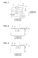
- FIG. 1 is a top view of the microchip related to the present invention.
- Fig. 2 is a cross-section of a portion of the microchip related to the present invention and a II-II section of Fig. 1.
- Fig. 3 is a cross-section of a portion of the microchip related to the present invention and a III-III section of Fig. 1 .
- Fig. 4 is a cross-section of a portion of the microchip related to the present invention and a IV-IV section of Fig. 1.
- Fig. 2 and Fig. 3 are cross-sectional views and Fig. 4 is a cross-sectional view of the through hole at a largest diameter.
- the microchip 1 related to the present embodiment is provided with a resinous substrate 2 and a resinous film 10.
- a resinous substrate 2 On a surface of the resinous substrate 2 a channel groove is formed.
- the resinous film 10 representing a counterpart of bonding with the resinous substrate 2 is a member in a shape of a sheet.
- the resinous substrate 2 and the resinous film 10 are bonded with the surface on which the channel is formed (bonding surface) inside.
- the resinous film 10 serves as a cover of the channel groove and a micro-channel 3 is formed, thus a microchip 1 having the micro channel 3 formed by the channel groove inside is manufactured.
- the micro channel 3 is configured with a bottom surface and walls of the channel groove, and a lower surface of the resinous film 10.
- through holes 4 are formed to penetrate in a direction of the thickness of the substrate.
- the through holes 4 are formed at ends or in mid-course of the channel groove.
- the opening section (through hole 4) is a hole to inlet, store and discharge gel, liquid regent or buffer liquid.
- a shape of the opening section (through hole 4) can be a cylindrical shape, a square shape or various shapes.
- a tube or a nozzle provided in the analyzer is connected to the opening (through hole 4) and gel, liquid regent or buffer liquid is inlet to the micro-channel 3 or discharged from the micro-channel 3.
- a resin is used in the resinous substrate 2 and the resinous film 10.
- resin conditions of the resin there are cited a preferable formability (transferability and releasability), a high transparency, and a low self-fluorescence with respect to ultraviolet ray and visible ray.
- a thermoplastic resin is used for the resinous substrate 2 and the resinous film 10.
- thermoplastic resin for example, polycarbonate, polymethacrylate methyl, polystyrene, polyacrylnitryl, polyvinyl chloride, polyethylene terephthalate, nylon 6, nylon 66, polyvinyl acetate, polyvinylidene chloride, polypropylene polyisoprene, polyethylene, polydimethylsiloxane, cyclic polyolefin are cited. More preferably polymethacrylate methyl and cyclic polyolefin are used. Incidentally, the same material or different materials can be used for the resinous substrate 2 and the resinous film 10.
- the resinous substrate 2 and the resinous film 10 are bonded via thermal fusion bonding.
- thermal fusion bonding For example, using a heat plate, heat wind, a heat roller, ultrasonic, vibration or laser, the resinous substrate 2 and the resinous film 10 are heated and bonded.
- a heat press machine heated heat plates nip the resinous substrate 2 and resinous film 10, then pressure is applied and kept for a predetermined time, whereby the resinous substrate 2 and the resinous film 10 are bonded.
- the size and shape of the resinous substrate 10 can be discretional as far as they facilitate handling and analysis, and a rectangular shape and a square shape are preferred. For example, 10 mm square to 200 mm square is preferable, and 10 mm square to 100 mm square is also preferable.
- the shape of the micro-channel 3 is preferred to be in the range of 10 ⁇ m to 200 ⁇ m in the width and the depth without being limited thereto, in view of saving of the amount of the analysis specimen and the reagent to be used, as well as forming accuracy, transferring characteristics and mold releasability of the metal mold.
- the width and the depth of the micro-channel 3 can be decided in accordance with use of the microchip.
- the shape of the cross-section of the micro-channel can be a rectangle or a curved shape.
- the thickness of the resinous substrate 2 in which the micro-channel 3 is formed is preferred to be 0.2 mm to 5 mm in view of forming characteristic and 0.5 mm to 2 mm is more preferable.
- the thickness of the resinous film 10 (in a shape of a sheet) serving as the cover to encloses the channel groove is preferred to be 30 ⁇ m to 300 ⁇ m, and 50 ⁇ m to 150 ⁇ m is more preferable.
- a sagging angle of the resinous film 10 will be described.
- the sagging angle is defined as an angle ⁇ which is formed with a tangent line at a discretional point on the lower surface 11 of the resinous film 10 forming a side of the micro-channel 3 and a bonding surface 12 between the resinous substrate 2 and the resinous film 10.
- a possibly range of the sagging angle ⁇ is 0 to 90°(0° ⁇ 90°).
- the above sagging angle represents the sagging angle of the resinous film 10 in the cross-section in a width direction at each position of the channel.
- the sagging angle of the resinous film 10 in the cross-section in the width direction at each position of the channel is hereinafter may called " a sagging angle of the resinous film 10 in the channel".
- a sagging amount t In a cross-section in the width direction of the micro-channel 3, a distance from a discretional point at the lower surface 11 of the resinous film 10 forming a side of the micro-channel 3 to the bonding surface 12 between the resinous substrate 2 and the resinous film 10 is defined as the sagging amount.
- the above distance is a length of a vertical line from the discretional point to a plane surface when the vertical line is drawn form the discretional point on the lower surface 11 of the resinous film 10 towards the plane surface which includes the bonding surface 12.
- the above sagging amount represents the sagging amount of the resinous film 10 in the cross-section in the width direction at each position of the channel.
- the sagging amount of the resinous film 10 in the cross-section in the width direction at each position of the channel is hereinafter may called as "sagging amount of the resinous film 10 in the channel".
- the resinous substrate 2 and the resinous film 10 have square outer shapes.
- the micro-channel 3 is configured with a plurality of channels 3A parallel to a direction of a side (Y direction) ofthe microchip and a plurality of channels 3B parallel to a direction (X direction) perpendicular to the aforesaid side. Namely, a longitudinal direction of the channel 3A and the Y direction are parallel each other and a longitudinal direction of the channel 3B and the X direction are parallel each other.
- the channel 3A and the channel 3B are straight channels respectively and perpendicular to each other.
- the micro-channel 3 is disaggregated into the channel 3A which is an element parallel to the Y direction and the channel 3B which is an element parallel to the X direction.
- the channel 3A which is an element parallel to the Y direction
- the channel 3B which is an element parallel to the X direction.
- an end of the channel 3B perpendicular to the channel 3A is connected to form the micro-channel 3.
- one side is parallel to the MD direction (Machine Direction) and another side perpendicular the aforesaid side is parallel to the TD direction (Transverse Direction).
- the MD direction denotes a flow direction of the resin at manufacturing the resinous film 10
- the TD direction denotes a direction perpendicular to the MD direction.
- the present embodiment focuses on the following two points to manufacture the microchip I by bonding the resinous substrate 2 and the resinous film 10.
- the resinous substrate 2 and the resinous film 10 are bonded. Specifically, by comparing a total length X of the plurality of the channels 3B which longitudinal direction is parallel to the X direction and a total length Y of the plurality of the channels 3A which longitudinal direction is parallel to the Y direction, the TD direction of the resinous film 10 is set to coincide with the direction having the longer length, then the resinous substrate 2 and the resinous film 10 are bonded.
- the plurality of the channels 3A and the plurality of the channels 3B are formed in the microchip 1 so that the total length X of the plurality of the channels 3B is longer than the total length Y ofthe plurality of the channels 3A.
- the channels 3B represents the first channel which is parallel to the first side
- the channels 3A represents the second channel which is parallel to the second side. Since the longitudinal direction of the channels 3B is parallel to the X direction, the resinous substrate 2 and the resinous film 10 are bonded in a state that the X direction of the resinous substrate 2 and the TD direction of the resinous film 10 are parallel each other. Whereby, the X direction and the TD direction becomes parallel each other and the Y direction and the MD direction become parallel each other.
- the width direction (Y direction) of the channel 3B coincides with the MD direction of the resinous film 10. Since the width direction of the channel 3B is perpendicular to the longitudinal direction of the channel 3B (X direction, TD direction), the width direction of the channel 3B becomes parallel to the MD direction of the resinous film 10. On the other hand, as Fig. 3 shows, the width direction (X direction) of the channel 3A coincides with the TD direction of the resinous film 10. Since the width direction of the channel 3A is perpendicular to the longitudinal direction (Y direction, MD direction) of the channel 3A, the width direction ofthe channel 3A becomes parallel to the TD direction of the resinous film 10.
- the microchip 1 is manufactured by bonding the resinous substrate 2 and the resinous film 10 via thermal fusion bonding.
- the resinous film 10 in case the resinous film 10 is heated, the resinous film 10 has a characteristic that the film tends to contract readily in the MD direction than in the TD direction.
- the sagging amount the resinous film 10 in the MD direction is less than a sagging amount of the resinous film in the TD direction.
- the sagging amount of the resinous film 10 in the MD direction is relatively small, and the sagging amount of the resinous film 10 in the TD direction is relatively large.
- the sagging angle of the resinous film 10 in the MD direction becomes smaller than the sagging angle in the TD direction. Namely, the sagging angle of the resinous film 10 in the MD direction becomes relatively small and the sagging angle of the resinous film 10 in the TD direction becomes relatively large.
- the resinous substrate 2 and the resinous film 10 are bonded in a way that the longitudinal direction (X direction) of the channel 3B having the longer total length and the TD direction in which the sagging amount is large are made parallel, and the longitudinal direction (Y direction) of the channel 3A having the shorter total length and the MD direction in which the sagging amount is small are made parallel.
- the width direction of the channel 3B having the longwe total length and MD direction having the small sagging amount are made parallel each other.
- the width direction ofthe channel 3B and the MD direction having the small sagging angle are made parallel.
- the width direction of the channel 3A having the shorter total length and the TD direction having a large sagging amount become parallel.
- the width direction of the channel 3A and the TD direction in which the sagging angle is large become parallel each other.
- the sagging of the resinous film 10 in the channel 3A having the shorter total length has a small contribution to sagging of the entire micro channel 3 in accordance with the short length of the channel 3A.
- the sagging amount of the resinous film 10 in the TD direction is relatively large, the sagging amount of the resinous film 10 in the TD direction has a large contribution to the sagging of the entire micro-channel 3.
- the microchip 1 related to the present embodiment by reducing a percentage of the TD direction with respect to the width direction of the micro-channel 3, the sagging amount of the entire micro-channel is reduced.
- the percentage of the TD direction with respect to the width direction of the micro-channel 3 can be reduced.
- the percentage of the TD direction having the large sagging mount can be reduced, the sagging amount in the entire micro-channel 3 can be reduced.
- the sagging angle of the entire micro-channel 3 can be reduced.
- the sagging of the resinous film 10 in the channel 3B having the long total length has a large contribution to the sagging of the entire micro channel 3 in accordance with the longer length of the channel 3A.
- the sagging amount ofthe resinous film in the MD direction is relatively small.
- the MD direction having the small sagging amount of the resinous film 10 parallel to the width direction of the channel 3B having the longer total (length, the sagging amount of the resinous film 10 in the channel 3B having a longer total length can be reduced.
- the sagging mount of the resinous film 10 in the channel 3B having the longwe total length can be reduced, the sagging amount in the entire micro-channel 3 can be reduced.
- the sagging angle of the entire micro-channel 3 can be reduced
- the sagging amount of the entire micro channel 3 can be reduced. Also, the sagging angle ofthe entire micro-channel 3 can be reduced. By reducing the sagging amount across the entire micro-channel 3, an error of the volume of the micro-channel can be reduced, thus analysis accuracy of the liquid specimen can be improved. Also, by reducing the sagging amount across the entire micro-channel 3, since the leakage of the liquid specimen from the microchip 1 can be inhibited, thus analysis accuracy ofthe liquid specimen can be improved.
- the sagging angle is defined as a sagging angle ⁇ 1
- the sagging amount is defined as a sagging amount t1.
- the sagging angle is defined as a sagging angle ⁇ 2
- the sagging amount is defined as a sagging amount t2.
- the width direction of the channel 3B and the MD direction are parallel and the width direction of the channel 3A and the TD direction are parallel each other. Therefore, the sagging amount t1 in the channel 3B having the longer total length is smaller than the sagging amount t2 in the channel 3A having the shorter total length (t1 ⁇ t2). Also, the sagging angle ⁇ 1 in the channel 3B is smaller than the sagging angle ⁇ 2 in the channel 3A ( ⁇ 1 ⁇ 2).
- the width direction of the channel 3B and the MD become parallel each other, and the width direction of the channel 3A and the TD direction become parallel each other.
- the sagging amount of the resinous film 10 across the entire micro-channel 3 can be reduced.
- the sagging angle across the entire micro-channel 3 can be reduced.
- the total length X of the channel 3B having the longer total length is preferred to be more than two times of the total length Y of the channel 3A having the shorter total length.
- the total length can be obtained from the straight channel excluding the curved channel. Namely, excluding the curved channel, the total length X of the lengths of the channels parallel to the X direction and the total length Y of the lengths of the channels parallel to the Y direction have only to be compared.
- the sagging angles ⁇ 1 and ⁇ 2 and the sagging amounts t1 and t2 are preferred to be the following values in view points of detection of the liquid reagent and flow ofthe liquid reagent.
- the sagging angles ⁇ 1 and ⁇ 2 are preferred to be 0° to 3 0° (0° ⁇ 1 ⁇ 30° and 0° ⁇ ⁇ 2 ⁇ 30°) and 0 to 10°(0° ⁇ ⁇ 1 ⁇ 10° and 0° ⁇ ⁇ 2 ⁇ 10°) are more preferred.
- values of the sagging amounts t1 and t2 with respect to the depth d of the micro-channel 3 are preferred to be 0 to 0.1 (0 ⁇ (t1 / d) ⁇ 0.1 and 0 ⁇ (t2 /d) ⁇ 0.1), and 0 to 0.05 (0 ⁇ (t1 / d) ⁇ 0.05 and 0 ⁇ (t2/d) ⁇ 0.05) are more preferable.
- the microchip 1 After bonding the resinous substrate 2 and the resinous film 10 via thermal fusion bonding, the microchip 1 can be subject to annealing. It is considered that occurrence of sagging of the resinous film 10 at the micro-channel 3 and the through hole 4 means that by expansion of the resinous film 10 covering the channel groove and the through hole 4 or by applying pressure, the thickness of the resinous film 10 was reduced, as a result the area of the film was increased then the film was pushed into the channel groove and the through hole 4 in accordance with the increase of the area. Thus, by contracting the resinous film 10, the sagging of the resinous film 10 can be reduced.
- the resinous film 10 contracts and as a result, the sagging of the resinous film can be reduced. Since conditions of annealing such as heating temperature and heating time varies with physical characteristics of the resinous film 1 a, the thickness, the width of the channel groove and the diameter of the through hole 4, the conditions will be determined for each microchip. As an example, the sagging of the resinous film 10 can be reduced by annealing the microchip at 90°C for one hour.
- a heating method for example, a method to heat the microchip by leaving in a heated atmosphere using a constant-temperature reservoir to heat, a method to heat the surface of the microchip partially using a heat blower and a method to heat by radiating ultra violet ray onto the resinous film using a UV radiation device.
- a longer heating time is effective to correct the sagging though there is a possibility of occurrence of deterioration of the resin, deformation of the micro-channel or deformation of the resinous substrate 2.
- the annealing conditions are adjusted so as not to occur the deterioration and deformations.
- FIG. 5 is a top view of the microchip related to the modification example 1.
- a microchip 1 A related to the modification example 1 is provided with a resinous substrate 20 having a channel groove formed on the surface thereof and a resinous film.
- a micro-channel 21 is formed with the channel groove by bonding the resinous substrate 20 and the resinous film, thus a microchip 1A having the micro-channel 21 by the channel groove inside is manufactured.
- through holes 22 to penetrate the substrate in the thickness direction are formed.
- the through holes 22 are formed at ends of the channel groove or in mind-course of the channel groove.
- the resinous substrate 20 and the resinous film have rectangle outer shapes, A length (length in X direction) of one side of the microchip 1 A is longer than a length (length in Y direction) of another side perpendicular to the aforesaid side.
- the micro-channel 21 is configured with a plurality of channels 21A parallel to a direction of the side (Y direction) of the microchip 1A and a plurality of channels 21B parallel to a direction (X direction) perpendicular to the side thereof Namely, a longitudinal direction of the channel 21A is parallel to the Y direction and a longitudinal direction of the channel 21B is parallel to the X direction.
- the channel 21A and the channel 21 B are straight channels and perpendicular to each other.
- the micro-channel 21 can be disaggregated into the channel 21A representing an element parallel to the Y direction and the channel 21 B representing an element parallel to the X direction. At an end of the channel 21A, an end of the channel 21 B perpendicular to the channel 21A is connected so as to configure the micro-channel, 21.
- one side is parallel to the MD direction and another side perpendicular to the aforesaid side is parallel to TD direction.
- the TD direction of the resinous film 10 is made to coincide with the direction having a longer total length. Then the resinous substrate 20 and the resinous film are bonded.
- the plurality of the channels 21 A and the plurality of the channels 21B are formed so that the total length X of the plurality of the channels 21 B is longer than the total length Y of the plurality of the channels 21A.
- the channel 21 B represents the first channel which is parallel to the first side and the channel 21 A represents the second channel which is parallel to the second side. Since the longitudinal direction of the channel 21 B is parallel to the X direction, the resinous substrate 20 and the resinous film are bonded in a state that the X direction of the resinous substrate 20 and the TD direction of the resinous film are parallel each other. Whereby, the X direction and the TD direction become parallel each other and the Y direction and the MD direction become parallel each other.
- the width direction (Y direction) of the channel 21 B and the MD direction of the resinous film coincide.
- the width direction (X direction) of the channel 21A coincides with the MD direction of the resinous film.
- the resinous substrate 20 and the resinous film is bonded in a way that that the longitudinal direction (X direction) of the channel 21B having the longer total length and the TD direction in which the sagging amount is large are made parallel, and the longitudinal direction (Y direction) of the channel 21 A having the shorter total length and the MD direction in which the sagging amount is small are made parallel.
- the sagging amount of entire micro-channel 21 is reduced and the sagging angle across the entire micro-channel 21 can be reduced in the same manner as in the aforesaid embodiment.
- Fig. 6 is a top view of the resinous substrate related to the modification example 2.
- the microchip related to the modification example 2 is provided with a resinous substrate 30 having a channel groove 31 formed on a surface thereof and a resinous film to be bonded onto the surface on which the channel groove 31 is formed.
- the micro-channel is formed by the channel groove 31, and a microchip having the micro-channel by the channel groove inside is manufactured.
- through holes 35 penetrating the substrate in the thickness direction are formed.
- the resinous substrate 30 and the resinous film have rectangular outer shapes.
- a length (length in the X direction) of one side of the resinous substrate 30 is longer than the length (length in the Y direction) of another side perpendicular to the aforesaid side.
- the channel groove 31 is, for example, in a Y character shape.
- the channel groove 31 is configured with a channel groove 32 parallel to a direction of one side (X direction) of the resinous substrate 31 and channel grooves 33 and 34 extending obliquely from an end of the channel groove 32 with respect to the channel groove 32.
- the channel grooves 33 and 34 are formed obliquely with respect to the side of the resinous substrate 30.
- the channel grooves 33 and 34 are formed obliquely but not parallel to the X and Y directions of the resinous substrate 3 Q.
- the channel grooves 33 and 34 are disaggregated into an element of X direction and an element ofY direction parallel to respective sides of the resinous substrate 30.
- the channel groove 33 will be described as an example.
- Fig. 6 shows, the channel groove 33 is disaggregated into a groove element 33A parallel to the Y direction and a groove element 33B parallel to the X direction.
- the channel groove 34 is also disaggregated into an element parallel to the X direction and an element parallel to the Y direction in the same manner.
- a total length X of a length ofthe channel groove which longitudinal direction is parallel to the X direction and a length of the groove element parallel to the X direction is obtained.
- a total length Y of a length of the groove element which longitudinal direction is parallel to the Y direction and a length of the groove element parallel to the Y direction is obtained. Then comparing the total length X and the total length Y, the resinous substrate 30 and the resinous film are bonded so that the direction having the longer total length is coincided with the TD direction of the resinous film.
- a total length X (a total of the first channel) is obtained.
- a total length Y (a total of the second channel) is obtained. Then based on the total length X and the total length Y, a longer channel is judged. Namely, by comparing the total length X and the total length Y, the resinous substrate 30 and the resinous film are bonded so that the TD direction of the resinous film is coincided with a direction having longer total length (first side).
- the resinous substrate 30 and the resinous film are bonded in a state that the X direction is a direction parallel to the first side, and the X direction of the resinous substrate 30 and the TD direction of the resinous film are parallel.
- the X direction and the TD direction become parallel
- the Y direction and the MD direction become parallel.
- the direction X having the longer total length including the length of the groove element and the TD direction in which the sagging amount is large are parallel
- the direction Y having the shorter total length including the length of the groove element and the MD direction in which the sagging amount is small are parallel.
- the width direction of the channel (Y direction) having the longer total length which includes the length of the groove element and the MD direction in which the sagging amounts is small become parallel
- the width direction of the channel (X direction) having the shorter total length which includes the length of the groove element and the TD direction in which the sagging amount is large become parallel.
- the sagging amount across the entire micro-channel can be reduced in the same manner as the aforesaid embodiment
- Fig. 7 is a top view of the resinous substrate related to the modification example 3.
- the microchip related to the modification example 3 is provided with a resinous substrate 40 having a channel groove 41 formed on a surface thereof and a resinous film to be bonded onto the surface on which the channel groove 41 is formed.
- the micro-channel is formed by the channel groove 41, and a microchip having the micro-channel by the channel groove inside is manufactured.
- through holes 45 penetrating the substrate in the thickness direction are formed.
- the resinous substrate 40 and the resinous film have a rectangular outer shape of which corners are curved.
- the channel groove 41 is, for example, in a Y character shape.
- the channel groove 41 is configured with a channel groove 42 in a straight line shape and channel grooves 43 and 44 extending obliquely from an end of the channel groove 42 with respect to the channel groove 42.
- the outer shape of the resinous substrate 40 is not a rectangular shape but includes curved portions.
- a smallest rectangle to surround the resinous substrate 40 which contacts with the outer shape of the resinous substrate 40 in a way that the contact portion of the rectangle is the maximum.
- Fig. 7 shows, there can be obtained a virtual rectangle 40A to surround the resinous substrate 40, which contacts with the outer shape of the resinous substrate 40.
- the rectangle is obtained so that the contact portion of the rectangle 40A is the maximum.
- a length (length in the X direction) of one side of the virtual rectangle 40A is longer than a length (length in the Y direction) of another side perpendicular to the aforesaid side.
- a longitudinal direction of the channel groove 42 is parallel to a side (in the X direction) of the rectangle 40A.
- the channel grooves 43 and 44 are formed obliquely with respect to the side of the virtual rectangle 40A.
- the channel grooves 43 and 44 are not parallel to the X and Y directions of the virtual rectangle 40A and formed obliquely.
- the channel grooves 43 and 44 are disaggregated into an element of X direction and an element of Y direction.
- the channel groove 43 is disaggregated into a groove element 43A (representing the first channel) parallel to the Y direction and a groove element 43B (representing the second channel) parallel to the X direction.
- the channel groove 44 is also disaggregated into an element parallel to the X direction and an element parallel to the Y direction.
- a total length X (total length of the first channel) of a length of the channel groove which longitudinal direction is parallel to the X direction and a length of the groove element parallel to the X direction is obtained.
- a total Y (total length of the second channel) of a length of the channel groove which longitudinal direction is parallel to the Y direction and a length of the groove element parallel to the Y direction is obtained. Then comparing the total length X and the total length Y, the resinous substrate 40 and the resinous film are bonded so that the direction having the longer total length (first side) is coincided with the TD direction ofthe resinous film.
- a total length X is obtained.
- a length of the groove element 43A and a length of the element in the Y direction of the channel groove 44 a total length Y is obtained.
- a total length Y is obtained.
- which channel is longer is judged. Namely, by comparing the total length X and the total length Y, the resinous substrate 40 and the resinous film are bonded so that the TD direction of the resinous film is coincided with the direction having the longer total length.
- the resinous substrate 40 and the resinous film are bonded in a state that the X direction is a direction parallel to the first side and the X direction of the virtual rectangle 40A and the TD direction of the resinous film are parallel.
- the X direction and the TD direction become parallel
- the Y direction and the MD direction become parallel each other.
- the direction X having the longer total length which includes the length of the groove element and the TD direction in which the sagging amount is large are parallel
- the direction Y having the shorter total length which includes the length of the groove element and the MD direction in which the sagging amount is small are parallel.
- the width direction of the channel (Y direction) having the longer total length which includes the length of the groove element and the MD direction in which the sagging amount is small become parallel
- the width direction of the channel (X direction) having the shorter total length which includes the length of the groove element and the TD direction in which the sagging amount is large become parallel.
- the sagging amount across the entire micro-channel can be reduced in the same manner as the aforesaid embodiment.
- annealing can be applied to the microchip.
- the total length of the channel having a longer total length is preferred to be more than two times of the total length of the channel having shorter total length.
- the micro-channel includes curved channels, the total length is obtained from the straight channel omitting the curved area thereof
- Fig. 8 is a table showing conditions of examples and comparison examples.
- microchip 1 is subject to annealing after the resinous substrate 2 and the resinous film 10 are bonded.
- a resinous substrate of channel side was manufactured with a injection mold machine by forming a transparent resin material of methyl methacrylate (acrylic family resin) (Delpet 70NH of Asahi Kasei Corporation), in which a channel groove having a width of 30 ⁇ m and a depth of 30 ⁇ m and a plurality of through holes 4 having an inner diameter of 2 mm are formed on a plate shape member having an outer dimensions of width of 25 mm x width of 25 mm x thickness of 1 mm.
- the depth 30 ⁇ m of the channel groove is defined as a design value of the channel.
- the above resinous substrate on the channel side represents an example of the resinous substrate 2 related to the aforesaid embodiment.
- the transparent resin material ofmethyl methacrylate (acrylic family resin) (Acryplane TM of Mitsubishi Rayon Co., Ltd. thickness: 75 ⁇ m) is cut into a width of 25 mm x a width of 25 mm.
- a microchip 1 is manufactured.
- a micro-channel 3 is formed by the channel groove and the resinous film 10.
- the micro-channel 3 is configured with a channel 3B parallel to the X direction and the channel 3A parallel to the Y direction.
- the total length Y of the channel 3B was 40 mm.
- the total length X of the charmel 3B was 60 mm.
- the total length X of the channel 3B is longer than the total length Y of the channel 3A. Also, a ratio (X/Y) of the total length X of the channel 3B to the total length Y of the channel 3A is 1.5.
- the resin film 10 is laminated on a bonding surface 12 of the resinous substrate 2 on which the channel groove is formed.
- the resinous film 10 is laminated on the resinous substrate 2 so that the longitudinal direction (X direction) of the channel 3 B and the TD direction of the resinous film 10 become parallel, and the longitudinal direction (Y direction) of the channel 3A and the MD direction of the resinous film 10 become parallel.
- the resinous substrate 2 and the resinous film 10 were nipped with thermal plates heated at a pressing temperature of 82°C and applied a pressure of 38 kgf/cm 2 , then maintained for 30 sec to bond the resinous substrate 2 and the resinous film 10.
- the microchip 1 was manufactured by the above bonding.
- the sagging amount of the resinous film 10 was measured with a confocal scanning laser displacement meter LT 9000 TM of Keyence Corporation.
- the sagging amount is calculated from displacements at a channel, the opening section (through hole4) and adjacent plane thereof by focusing the laser on the outermost surface of the film with an outer shape measuring mode.
- the sagging amounts are measure at a plurality ofpoints and an average value was obtained.
- the depths of the channels 3A and 3B were measured to obtain deviations from the design value of depth (30 ⁇ m), Laser light was focused on the lower surface of the film (channel upper surface) and a bottom surface of the channel while the surfaces thereof being scanned by the laser light, and the depth was calculated from displacements of the two surfaces. The depths were measured at a plurality of points and an average value was obtained.
- the microchip 1 was annealed by keeping the microchip 1 in a constant-temperature reservoir at 90°C for one hour. After annealing, the sagging amount of the resinous film 10 in the micro-channel was measured. Also, by measuring the depths of the channels 3A and 3B, the deviation from the design value of the depth (30 ⁇ m) was obtained
- a glutirous polymer liquid (poly dimethylacrylamide, pDMA) was filled from a well (opening section). Since the substrate formed by PMMA has a hydrophilic nature, capillary action can be used for filling. The polymer liquid was filled in each well so that liquid levels are equated.
- fluorescent labeled DNA having a base pairs number of 100bp to 1,000bp was dripped into specimen filling well (opening section), then a direct current was applied to inlet and to separate. Using a cofocal laser microscope to energize and detect at a predetermined detection section, it was observed that plug (band) of the DNA was separated while forming a plug flow.
- the same electrophoresis was carried out ten times and by calculating variation of fluorescence intensity, reproducibility of detection of the analysis object (DNA) was obtained.
- the reproducibility indicates the variation of the fluorescence intensity. Namely a smaller value of reproducibility means a smaller variation of the fluorescence intensity, In the example 1, an excellent result of the reproducibility of 5 % was shown. As above, in the example 1, the variation of the fluorescence intensity was able to be reduced.
- the ratio between the total length Y of the channel 3A and the total length Y of the channel 3B was changed.
- the total length Y of the channel 3A was 20 mm.
- the total length X of the channel 3B was 100 mm.
- the resinous substrate 2 and the resinous film 10 are laminated in a way that the longitudinal direction of the channel 3B (X direction) and the TD direction of the resinous film 10 are parallel each other, and the longitudinal direction of the channel 3A (Y direction) and the MD direction of the resinous film 10 are parallel each other.
- the resinous substrate 2 and the resinous film 10 were bonded each other in the same conditions as in the example 1 and the microchip 1 was annealed in the same conditions. Then in the same manner as the example 1, the sagging amount of the resinous film 10 in the micro-channel 3 and the depth of the micro-channel 3 were measured before and after the annealing.
- An electrophoresis test was carried out under the same conditions as the example 1. The same electrophoresis was carried out ten times and by calculating variation of fluorescence intensity of the detection section, reproducibility of detecting the analysis object was obtained. An excellent result of the reproducibility of 3 % was shown. Further, compared to the example 1, higher detection sensitivity was confirmed. An experiment of the detection sensitivity was carried out with an index that how much a density of the DNA can be lowered while detection is possible.
- the total length Y of the channel 3A was 40 mm and the total length X ofthe channel 3B was 60 mm.
- a ratio (X/Y) of the total length X of the channel 3B to the total length Y of the channel 3A is 1.5.
- the total length X ofthe channel 3B is longer than the total length Y of the channel 3A. Therefore, in the comparison example 1, the resinous film 10 is laminated on the resinous substrate 2 so that the longitudinal direction (X direction) of the channel 3B and the MD direction of the resinous film 10 become parallel, and the longitudinal direction (Y direction) of the channel 3A and the TD direction ofthe resinous film 10 become parallel.
- the total length Y of the channel 3A was 20 mm and the total length X of the channel 3B was 100 mm.
- the ratio (X/Y) of the total length X of the channel 3B to the total length Y of the channel 3A was 5.
- the total length X of the channel 3B is longer than the total length Y of the channel 3A. Therefore, in the comparison example 2, the resinous film 10 is laminated on the resinous substrate 2 so that the longitudinal direction (X direction) of the channel 3B and the MD direction of the resinous film 10 become parallel, and the longitudinal direction (Y direction) of the channel 3A and the TD direction of the resinous film 10 become parallel.
- the sagging amount was possible to be reduced. Also, the error of the depth ofthe micro channel was possible to be lowered. Further as to the detection sensitivity and reproducibility of the analysis object, more preferable results were obtained than that of the comparison examples.
- the materials and the dimensions indicated in the aforesaid examples are examples without the invention being limited to the materials and the dimensions thereof
- the same results as the examples can be obtained.
- the microchips related to the modification examples 1 and 2 the same results as the examples can be obtained.
Landscapes
- Engineering & Computer Science (AREA)
- Mechanical Engineering (AREA)
- Chemical & Material Sciences (AREA)
- Physics & Mathematics (AREA)
- Health & Medical Sciences (AREA)
- Thermal Sciences (AREA)
- Manufacturing & Machinery (AREA)
- Analytical Chemistry (AREA)
- Dispersion Chemistry (AREA)
- Life Sciences & Earth Sciences (AREA)
- Molecular Biology (AREA)
- General Health & Medical Sciences (AREA)
- Chemical Kinetics & Catalysis (AREA)
- Microelectronics & Electronic Packaging (AREA)
- Biochemistry (AREA)
- Hematology (AREA)
- Electrochemistry (AREA)
- Clinical Laboratory Science (AREA)
- General Physics & Mathematics (AREA)
- Immunology (AREA)
- Pathology (AREA)
- Automatic Analysis And Handling Materials Therefor (AREA)
- Micromachines (AREA)
- Physical Or Chemical Processes And Apparatus (AREA)
Abstract
Description
- The present invention relates to a microchip manufactured by bonding a resinous substrate on which a channel groove is formed and a microchip manufacturing method.
- There are practically used devices so called a micro analysis chip, or a µTAS (Micro Total Analysis System) in which a micro-channel and a circuitry are formed on a silicon or a glass substrate via a micro technology so as to perform a chemical reaction, isolation and analysis of liquid specimens such as nucleic acid, protein and blood in a micro space. As a merit of the micro channel chip, it is considered that there is realized a space saving, portable and economical system which reduces amounts of sample and reagent used and an emission amount of waste liquid.
- The microchip is manufactured by bonding two members wherein a microstructure is formed at least one member. Conventionally, a glass substrate is used for the microchip and various forming methods of forming the micro structure are suggested. However, since the glass substrate is not suitable for mass production and very costly, development of a low cost and disposable resinous microchip has been desired.
- To manufacture the resinous microchip, a resinous substrate having a channel groove on a surface thereof and a resinous film to cover the channel groove are bonded. In the resinous substrate having the channel groove, through holes penetrating in a thickness direction of the resinous substrate are formed at ends of the channel groove and the like. The resinous substrate having the channel groove on the surface thereof is bonded with the resinous film for a cover with the channel groove inside. By the above bonding, the resinous film for the cover serves as a cover of the channel groove, thus a channel is formed with the channel groove and the resinous film. Whereby, the microchip having the channel inside is manufactured. Via the through holes formed on the resinous substrate, the channel and an outside of the microchip are connected, and liquid specimen enters and exits via the through holes.
- As the method to bond the resinous substrate and the resinous film, there are cited a method to use an adhesive, a method to dissolve the resin surface for bonding, a method to use an ultrasonic wielding, a method to use laser welding, and a method to use thermal fusion bonding via a pressure device having a role shape or a flat shape. Among the above methods, thermal fusion bonding is suitable as a bonding method, assuming mass production since it can be practiced at a low cost.
- As the above microchip, there is suggested a microchip in which onto an acryl family resinous substrate such as polymethylacrylate, the same acryl family resinous film is bonded via thermal fusion bounding.
- Patent Document 1: Unexamined Japanese Patent Application Publication No.
2000-310613 - Based on a disclosure in the
above Patent Document 1, the resinous substrate and the resinous film were bonded, however it was found that the resinous film sagged into the channel and the through hole. A cause of the resinous film bonded with sagging was revealed that the resinous film softened by heat is pushed into a space of the channel or the through hole by pressure. - In the state that the film is sagging into the channel groove, the channel formed by the channel groove and the resinous film becomes smaller that an original cross-section shape (rectangle or trapezium). Thus a flow speed of the liquid specimen flowing in the channel is reduced, and a variation of the flow speed occurs. As a result, an accurate measuring of the liquid specimen becomes difficult.
- Also, the volume of the channel varies in accordance with the nature of sagging of the resinous film into the channel, an amount of the liquid specimen filling the channel varies. By the variation of the volume of the channel, a flowing direction and the flowing speed of the liquid specimen in the channel are effected. A large variation, namely a low quantitativeness, is a serious problem to carry out analysis of the liquid specimen. Also, by the variation of the volume of the channel, there is a problem that reproducibility is deteriorated.
- Further by an increase of the sagging of the resinous film, the liquid specimen may leaks outside the microchip from a sagging portion of the resinous film in the channel. If the liquid specimen leaks out from the microchip, the quantitativeness of the liquid specimen is deteriorated and as a result, there is a problem such that analysis accuracy of the liquid specimen is deteriorated.
- As above, in the microchip related to the prior art, by the sagging of the resinous film, the volume of the channel varies, and leakage of the liquid specimen occurs. As a result, there was a problem such that the analysis accuracy is deteriorated.
- On aspect of the present invention is to resolve the above problem and an object of the present invention is to provide a microchip capable of inhibiting sagging of the resinous film and a manufacturing method of the microchip thereof
- The present invention is focused on that the resinous film has different thermal contraction ratio in a MD direction and a TD direction of the resinous film. Here, the MD direction denotes a flowing direction of the film at manufacturing the film and the TD direction denotes a direction perpendicular to the MD direction.
- A first embodiment of the present invention is a microchip in which a channel is formed having a resinous substrate having a substantially rectangular outer shape in which a channel groove is formed, and a resinous film to form the channel by being bonded onto a surface of the resinous substrate on which the channel groove is formed, wherein a total length of a first channel parallel to a first side of the resinous substrate is longer than a total length of a second channel parallel to a second side, perpendicular to the first side, of the resinous substrate, of the resinous substrate, and the resinous substrate and the resinous film are bonded in a way that the first side and a TD direction of the resinous film are parallel and the second side and a MD direction of the resinous film are parallel.
- Also a second embodiment of the present invention is a microchip in which a channel is formed having: a resinous substrate in which a channel groove is formed, and a resinous film to form the channel by being bonded onto a surface of the resinous substrate on which the channel groove is formed, wherein when the channel is disaggregated into a first channel representing an element parallel to a first side of a virtual rectangle surrounding the resinous substrate defined to be in contact with a periphery of the resinous substrate and a second channel representing an element parallel to a second channel perpendicular to the first side, a total length of the first channel is longer than a total length of the second channel, wherein the resinous substrate and the resinous film are bonded in a way that the first side and a TD direction of the resinous film are parallel and the second side and a MD direction of the resinous film are parallel.
- Further, a third embodiment of the present invention is the microchip of the first or second embodiment, wherein the total length of the first channel is more than two times of the total length of the second channel.
- Also, a fourth embodiment of the present invention is a manufacturing method of a microchip having a channel, having: bonding a resinous film via thermal fusion bonding onto a surface of a resinous substrate on which a channel groove is formed, wherein the resinous substrate in which the channel groove is formed, is in a substantially rectangular shape, wherein a total of a length of a first channel parallel to a first side of the resinous substrate is longer than a total of a length of a second channel parallel to a second side, perpendicular to the first side, of the resinous substrate, of the resinous substrate, and the resinous substrate and the resinous film are bonded in a way that the first side and a TD direction of the resinous film are parallel and the second side and a MD direction of the resinous film are parallel.
- Also, a fifth embodiment of the present invention is a manufacturing method of a microchip having a channel, having: bonding a resinous film via thermal fusion bonding onto a surface of a resinous substrate on which a channel groove is formed, wherein the channel groove is formed in the resinous substrate, wherein when the channel is disaggregated into a first channel representing an element parallel to a first side of a virtual rectangle surrounding the resinous substrate defined to be in contact with a periphery of the resinous substrate and a second channel representing an element parallel to a second channel perpendicular to the first side, a total length of the first channel is longer than a total length of the second channel, wherein the resinous substrate and the resinous film are bonded in a way that the first side and a TD direction of the resinous film are parallel and the second side and a MD direction of the resinous film are parallel.
- Also, a sixth embodiment of the present invention is the manufacturing method of the microchip of the forth or fifth embodiment, wherein the total length of the first channel is more than two times of the total length ofthe second channel.
- Also, a seventh embodiment of the present invention is the manufacturing method of the microchip of any one of the forth to sixth embodiments, wherein a sagging amount of the resinous film in a cross-section in a width direction of the first channel is smaller that a sagging amount of the resinous film in a cross-section in a width direction of the second channel.
- Also, an eight embodiment of the present invention is the manufacturing method of the microchip ofany one of the forth to seventh embodiments wherein a sagging angle of the resinous film in a cross-section in a width direction of the first channel is smaller that a sagging angle of the resinous film in a cross-section in a width direction of the second channel.
- Also, a ninth embodiment of the present invention is the manufacturing method of the microchip of any one of the forth to eighth embodiments, wherein the bonded resinous substrate and the resinous film is subject to annealing at a predetermined temperature.
- According to the present invention, the first side parallel to the first channel having a longer total length is made parallel to the TD direction of the resinous film, and the second side parallel to the second channel having a shorter total length is made parallel to the MD direction, whereby the width direction ofthe first channel and the MD direction having less sagging becomes parallel. Thus, since the sagging decreases in the width direction of the first channel having the longer total length, the sagging of the entire channel can be reduced.
-
-
Fig. 1 is a top view of a microchip related to an embodiment of the present invention. -
Fig. 2 is a cross-sectional view of a microchip related to an embodiment of the present invention and a II-II section ofFig. 1 . -
Fig. 3 is a cross-sectional view of a microchip related to an embodiment of the present invention and a II-III section ofFig. 1 . -
Fig. 4 is a cross-sectional view of a microchip related to an embodiment of the present invention and a IV-IV section ofFig. 1 . -
Fig. 5 is a top view of a microchip related to a modification example 1. -
Fig. 6 is a top view of a resinous substrate related to a modification example 2. -
Fig. 7 is a top view of a resinous substrate related to a modification example 3. -
Fig. 8 is a table showing conditions of examples and comparison examples. - A microchip related to an embodiment of the present invention will be described with reference to
Fig. 1 toFig. 4 .Fig. 1 is a top view of the microchip related to the present invention.Fig. 2 is a cross-section of a portion of the microchip related to the present invention and a II-II section ofFig. 1. Fig. 3 is a cross-section of a portion of the microchip related to the present invention and a III-III section ofFig. 1 .Fig. 4 is a cross-section of a portion of the microchip related to the present invention and a IV-IV section ofFig. 1. Fig. 2 and Fig. 3 are cross-sectional views andFig. 4 is a cross-sectional view of the through hole at a largest diameter. - As
Fig. 1 to Fig. 3 show, themicrochip 1 related to the present embodiment is provided with aresinous substrate 2 and aresinous film 10. On a surface of the resinous substrate 2 a channel groove is formed. Theresinous film 10 representing a counterpart of bonding with theresinous substrate 2 is a member in a shape of a sheet. Theresinous substrate 2 and theresinous film 10 are bonded with the surface on which the channel is formed (bonding surface) inside. Whereby, theresinous film 10 serves as a cover of the channel groove and amicro-channel 3 is formed, thus amicrochip 1 having themicro channel 3 formed by the channel groove inside is manufactured. Themicro channel 3 is configured with a bottom surface and walls of the channel groove, and a lower surface of theresinous film 10. - Also, as
Fig. 1 andFig. 4 show, in theresinous substrate 2, throughholes 4 are formed to penetrate in a direction of the thickness of the substrate. The throughholes 4 are formed at ends or in mid-course of the channel groove. By bonding theresinous substrate 2 and theresinous film 10 the through holes become opening sections which connect the micro channel with an outside. Since the throughhole 4 is connected with the channel groove, the opening section of the throughhole 4 is connected with themicro-channel 3. The opening section (through hole 4) is a hole to inlet, store and discharge gel, liquid regent or buffer liquid. A shape of the opening section (through hole 4) can be a cylindrical shape, a square shape or various shapes. A tube or a nozzle provided in the analyzer is connected to the opening (through hole 4) and gel, liquid regent or buffer liquid is inlet to themicro-channel 3 or discharged from themicro-channel 3. - A resin is used in the
resinous substrate 2 and theresinous film 10. As resin conditions of the resin, there are cited a preferable formability (transferability and releasability), a high transparency, and a low self-fluorescence with respect to ultraviolet ray and visible ray. For example, a thermoplastic resin is used for theresinous substrate 2 and theresinous film 10. As the thermoplastic resin, for example, polycarbonate, polymethacrylate methyl, polystyrene, polyacrylnitryl, polyvinyl chloride, polyethylene terephthalate, nylon 6, nylon 66, polyvinyl acetate, polyvinylidene chloride, polypropylene polyisoprene, polyethylene, polydimethylsiloxane, cyclic polyolefin are cited. More preferably polymethacrylate methyl and cyclic polyolefin are used. Incidentally, the same material or different materials can be used for theresinous substrate 2 and theresinous film 10. - The
resinous substrate 2 and theresinous film 10 are bonded via thermal fusion bonding. For example, using a heat plate, heat wind, a heat roller, ultrasonic, vibration or laser, theresinous substrate 2 and theresinous film 10 are heated and bonded. As an example, using a heat press machine, heated heat plates nip theresinous substrate 2 andresinous film 10, then pressure is applied and kept for a predetermined time, whereby theresinous substrate 2 and theresinous film 10 are bonded. - The size and shape of the
resinous substrate 10 can be discretional as far as they facilitate handling and analysis, and a rectangular shape and a square shape are preferred. For example, 10 mm square to 200 mm square is preferable, and 10 mm square to 100 mm square is also preferable. - The shape of the
micro-channel 3 is preferred to be in the range of 10 µm to 200 µm in the width and the depth without being limited thereto, in view of saving of the amount of the analysis specimen and the reagent to be used, as well as forming accuracy, transferring characteristics and mold releasability of the metal mold. Also, the width and the depth of the micro-channel 3 can be decided in accordance with use of the microchip. Incidentally, the shape of the cross-section of the micro-channel can be a rectangle or a curved shape. - The thickness of the
resinous substrate 2 in which themicro-channel 3 is formed is preferred to be 0.2 mm to 5 mm in view of forming characteristic and 0.5 mm to 2 mm is more preferable. The thickness of the resinous film 10 (in a shape of a sheet) serving as the cover to encloses the channel groove is preferred to be 30 µm to 300 µm, and 50 µm to 150 µm is more preferable. - Here, the sagging of the
resinous film 10 towards the channel groove when theresinous substrate 2 and theresinous film 10 are bonded will be described. - A sagging angle of the
resinous film 10 will be described. In the cross-section in tle width direction of themicro-channel 3, the sagging angle is defined as an angle θ which is formed with a tangent line at a discretional point on thelower surface 11 of theresinous film 10 forming a side of themicro-channel 3 and abonding surface 12 between theresinous substrate 2 and theresinous film 10. If the wall of the channel groove of theresinous substrate 2 is perpendicular to thebonding surface 12, a possibly range of the sagging angle θ is 0 to 90°(0°≤θ≤90°). Incidentally, the above sagging angle represents the sagging angle of theresinous film 10 in the cross-section in a width direction at each position of the channel. The sagging angle of theresinous film 10 in the cross-section in the width direction at each position of the channel is hereinafter may called " a sagging angle of theresinous film 10 in the channel". - Next a sagging amount t will be described. In a cross-section in the width direction of the
micro-channel 3, a distance from a discretional point at thelower surface 11 of theresinous film 10 forming a side of the micro-channel 3 to thebonding surface 12 between theresinous substrate 2 and theresinous film 10 is defined as the sagging amount. The above distance is a length of a vertical line from the discretional point to a plane surface when the vertical line is drawn form the discretional point on thelower surface 11 of theresinous film 10 towards the plane surface which includes thebonding surface 12. Incidentally, the above sagging amount represents the sagging amount of theresinous film 10 in the cross-section in the width direction at each position of the channel. The sagging amount of theresinous film 10 in the cross-section in the width direction at each position of the channel is hereinafter may called as "sagging amount of theresinous film 10 in the channel". - In the above embodiment, as
Fig. 1 shows, theresinous substrate 2 and theresinous film 10 have square outer shapes. Also, themicro-channel 3 is configured with a plurality ofchannels 3A parallel to a direction of a side (Y direction) ofthe microchip and a plurality ofchannels 3B parallel to a direction (X direction) perpendicular to the aforesaid side. Namely, a longitudinal direction of thechannel 3A and the Y direction are parallel each other and a longitudinal direction of thechannel 3B and the X direction are parallel each other. Thechannel 3A and thechannel 3B are straight channels respectively and perpendicular to each other. As above, themicro-channel 3 is disaggregated into thechannel 3A which is an element parallel to the Y direction and thechannel 3B which is an element parallel to the X direction. At an end of thechannel 3A, an end of thechannel 3B perpendicular to thechannel 3A is connected to form themicro-channel 3. - In the
resinous film 10 having the square shape, one side is parallel to the MD direction (Machine Direction) and another side perpendicular the aforesaid side is parallel to the TD direction (Transverse Direction). The MD direction denotes a flow direction of the resin at manufacturing theresinous film 10, and the TD direction denotes a direction perpendicular to the MD direction. - The present embodiment focuses on the following two points to manufacture the microchip I by bonding the
resinous substrate 2 and theresinous film 10. - (1) There is a difference in the thermal contraction ratio between the MD direction and the TD direction,
- (2) In the microchip, the micro-channel is often designed to reciprocate so as to earn the length of the micro-channel. When this occurs, in the micro-channel, in order to increase the percentage of straight portions, a percentage of the straight portions parallel to a direction is increased.
- Focusing the above tow points, the
resinous substrate 2 and theresinous film 10 are bonded. Specifically, by comparing a total length X of the plurality of thechannels 3B which longitudinal direction is parallel to the X direction and a total length Y of the plurality of thechannels 3A which longitudinal direction is parallel to the Y direction, the TD direction of theresinous film 10 is set to coincide with the direction having the longer length, then theresinous substrate 2 and theresinous film 10 are bonded. - In the
microchip 1 shown byFig. 1 , the plurality of thechannels 3A and the plurality of thechannels 3B are formed in themicrochip 1 so that the total length X of the plurality of thechannels 3B is longer than the total length Y ofthe plurality of thechannels 3A. As above, in the embodiment shown inFig. 1 , thechannels 3B represents the first channel which is parallel to the first side, and thechannels 3A represents the second channel which is parallel to the second side. Since the longitudinal direction of thechannels 3B is parallel to the X direction, theresinous substrate 2 and theresinous film 10 are bonded in a state that the X direction of theresinous substrate 2 and the TD direction of theresinous film 10 are parallel each other. Whereby, the X direction and the TD direction becomes parallel each other and the Y direction and the MD direction become parallel each other. - By bonding the
resinous substrate 2 and theresinous substrate 10 in the above manner, asFig. 2 shows, the width direction (Y direction) of thechannel 3B coincides with the MD direction of theresinous film 10. Since the width direction of thechannel 3B is perpendicular to the longitudinal direction of thechannel 3B (X direction, TD direction), the width direction of thechannel 3B becomes parallel to the MD direction of theresinous film 10. On the other hand, asFig. 3 shows, the width direction (X direction) of thechannel 3A coincides with the TD direction of theresinous film 10. Since the width direction of thechannel 3A is perpendicular to the longitudinal direction (Y direction, MD direction) of thechannel 3A, the width direction ofthechannel 3A becomes parallel to the TD direction of theresinous film 10. - The
microchip 1 is manufactured by bonding theresinous substrate 2 and theresinous film 10 via thermal fusion bonding. As above, in case theresinous film 10 is heated, theresinous film 10 has a characteristic that the film tends to contract readily in the MD direction than in the TD direction. Thus when theresinous film 10 is bonded onto theresinous substrates 2 via thermal fusion bonding, the sagging amount theresinous film 10 in the MD direction is less than a sagging amount of the resinous film in the TD direction. Namely, in case theresinous substrate 2 and theresinous film 10 are bonded via thermal fusion bonding, the sagging amount of theresinous film 10 in the MD direction is relatively small, and the sagging amount of theresinous film 10 in the TD direction is relatively large. Also, the sagging angle of theresinous film 10 in the MD direction becomes smaller than the sagging angle in the TD direction. Namely, the sagging angle of theresinous film 10 in the MD direction becomes relatively small and the sagging angle of theresinous film 10 in the TD direction becomes relatively large. - In the present embodiment, the
resinous substrate 2 and theresinous film 10 are bonded in a way that the longitudinal direction (X direction) of thechannel 3B having the longer total length and the TD direction in which the sagging amount is large are made parallel, and the longitudinal direction (Y direction) of thechannel 3A having the shorter total length and the MD direction in which the sagging amount is small are made parallel. - As above, by bonding the
resinous substrate 2 and theresinous film 2 so flat the MD direction in which the sagging amount of theresinous film 10 is small and the longitudinal direction (Y direction) of thechannel 3A having the shorter total length are made parallel, asFig. 2 shows, the width direction of thechannel 3B having the longwe total length and MD direction having the small sagging amount are made parallel each other. Also the width direction ofthechannel 3B and the MD direction having the small sagging angle are made parallel. On the other hand by bonding theresinous substrate 2 and theresinous film 10 in a way that the TD direction having large sagging amount of theresinous film 10 and the longitudinal direction (X direction) of thechannel 3B having the longer total length are made parallel, asFig. 3 shows, the width direction of thechannel 3A having the shorter total length and the TD direction having a large sagging amount become parallel. Also, the width direction of thechannel 3A and the TD direction in which the sagging angle is large become parallel each other. - The sagging of the
resinous film 10 in thechannel 3A having the shorter total length has a small contribution to sagging of the entiremicro channel 3 in accordance with the short length of thechannel 3A. On the other hand, since the sagging amount of theresinous film 10 in the TD direction is relatively large, the sagging amount of theresinous film 10 in the TD direction has a large contribution to the sagging of theentire micro-channel 3. In themicrochip 1 related to the present embodiment, by reducing a percentage of the TD direction with respect to the width direction of themicro-channel 3, the sagging amount of the entire micro-channel is reduced. For example, by making the TD direction having the large sagging amount of theresinous film 10 parallel to the width direction of thechannel 3A having the short total length, the percentage of the TD direction with respect to the width direction of the micro-channel 3 can be reduced. As above since the percentage of the TD direction having the large sagging mount can be reduced, the sagging amount in theentire micro-channel 3 can be reduced. Also, by making the TD direction in which the sagging angle is large parallel to the width direction of thechannel 3A having the longer total length, the sagging angle of theentire micro-channel 3 can be reduced. - Also, the sagging of the
resinous film 10 in thechannel 3B having the long total length has a large contribution to the sagging of the entiremicro channel 3 in accordance with the longer length of thechannel 3A. On the other hand, since the sagging amount ofthe resinous film in the MD direction is relatively small. Thus by making the MD direction having the small sagging amount of theresinous film 10 parallel to the width direction of thechannel 3B having the longer total (length, the sagging amount of theresinous film 10 in thechannel 3B having a longer total length can be reduced. As above, since the sagging mount of theresinous film 10 in thechannel 3B having the longwe total length can be reduced, the sagging amount in theentire micro-channel 3 can be reduced. Also, by making the MD direction in which the sagging angle is small parallel to the width direction of thechannel 3B having the longer total length, the sagging angle of theentire micro-channel 3 can be reduced - As above, by bonding the
resinous substrate 2 and theresinous film 10 in the way that the width direction of thechannel 3A having the shorter total length is made parallel to the TD direction of theresinous film 10, and the width direction of thechannel 3B having the longer total length is made parallel to the MD direction of theresinous film 10, the sagging amount of the entiremicro channel 3 can be reduced. Also, the sagging angle oftheentire micro-channel 3 can be reduced. By reducing the sagging amount across theentire micro-channel 3, an error of the volume of the micro-channel can be reduced, thus analysis accuracy of the liquid specimen can be improved. Also, by reducing the sagging amount across theentire micro-channel 3, since the leakage of the liquid specimen from themicrochip 1 can be inhibited, thus analysis accuracy ofthe liquid specimen can be improved. - Here the sagging angle θ and the sagging amount t of the
resinous film 10 in the channel will be described with reference toFig. 2 and Fig. 3 - As
Fig. 2 shows, in thechannel 3B, the sagging angle is defined as a sagging angle θ1, and the sagging amount is defined as a sagging amount t1. On the other hand, asFig. 3 shows, in thechannel 3A, the sagging angle is defined as a sagging angle θ2, and the sagging amount is defined as a sagging amount t2. - In the present embodiment, the width direction of the
channel 3B and the MD direction are parallel and the width direction of thechannel 3A and the TD direction are parallel each other. Therefore, the sagging amount t1 in thechannel 3B having the longer total length is smaller than the sagging amount t2 in thechannel 3A having the shorter total length (t1 < t2). Also, the sagging angle θ1 in thechannel 3B is smaller than the sagging angle θ2 in thechannel 3A (θ1<θ2). - As above, by bonding the
resinous substrate 2 and theresinous film 10 in the way that the longitudinal direction ofthechannel 3B having the longer total length is made parallel to the TD direction, and the longitudinal direction of thechannel 3A having the shorter total length is made parallel to the MD direction, the width direction of thechannel 3B and the MD become parallel each other, and the width direction of thechannel 3A and the TD direction become parallel each other. Thus the sagging amount of theresinous film 10 across theentire micro-channel 3 can be reduced. Also, the sagging angle across theentire micro-channel 3 can be reduced. - The total length X of the
channel 3B having the longer total length is preferred to be more than two times of the total length Y of thechannel 3A having the shorter total length. By making the total length more than two times, the percentage of the TD direction is reduced, thus the contribution to the sagging of theresinous film 10 in the TD direction is reduced As the result, the sagging amount across theentire micro-channel 3 is reduced and the sagging angle can be reduced. - Incidentally, in case the micro-channel includes a curved channel, the total length can be obtained from the straight channel excluding the curved channel. Namely, excluding the curved channel, the total length X of the lengths of the channels parallel to the X direction and the total length Y of the lengths of the channels parallel to the Y direction have only to be compared.
- Incidentally, the sagging angles θ1 and θ2 and the sagging amounts t1 and t2 are preferred to be the following values in view points of detection of the liquid reagent and flow ofthe liquid reagent. The sagging angles θ1 and θ2 are preferred to be 0° to 3 0° (0°≤θ1 < 30° and 0°≤ θ2 < 30°) and 0 to 10°(0°≤ θ1 < 10° and 0°≤ θ2 < 10°) are more preferred. Also values of the sagging amounts t1 and t2 with respect to the depth d of the micro-channel 3 (
channels - To measure the sagging angle and the sagging amount, a confocal scanning laser microscopy OLS 3000™ of Olympus Corporation was used. With a laser source of wave length λ=408 nm, a confocal optical system and a precision scanning mechanism, a highly accurate measuring is possible.
- In case of measuring the sagging angle of the lower surface of the
resinous film 10 forming a portion of themicro-channel 3, by radiating a laser light from an upper surface side of theresinous film 10, thelower surface 11 and thebonding surface 12 of theresinous film 10 were scanned by a laser focus and a three-dimensional shape of thelower surface 11 of theresinous film 10 was obtained. Then based on the three-dimensional shape, the sagging angle and the sagging amount of each position of the cross-section were obtained. - After bonding the
resinous substrate 2 and theresinous film 10 via thermal fusion bonding, themicrochip 1 can be subject to annealing. It is considered that occurrence of sagging of theresinous film 10 at themicro-channel 3 and the throughhole 4 means that by expansion of theresinous film 10 covering the channel groove and the throughhole 4 or by applying pressure, the thickness of theresinous film 10 was reduced, as a result the area of the film was increased then the film was pushed into the channel groove and the throughhole 4 in accordance with the increase of the area. Thus, by contracting theresinous film 10, the sagging of theresinous film 10 can be reduced. For example by heating themicrochip 1 up to around a glass transition temperature, theresinous film 10 contracts and as a result, the sagging of the resinous film can be reduced. Since conditions of annealing such as heating temperature and heating time varies with physical characteristics of the resinous film 1 a, the thickness, the width of the channel groove and the diameter of the throughhole 4, the conditions will be determined for each microchip. As an example, the sagging of theresinous film 10 can be reduced by annealing the microchip at 90°C for one hour. - As a heating method, for example, a method to heat the microchip by leaving in a heated atmosphere using a constant-temperature reservoir to heat, a method to heat the surface of the microchip partially using a heat blower and a method to heat by radiating ultra violet ray onto the resinous film using a UV radiation device. Also, a longer heating time is effective to correct the sagging though there is a possibility of occurrence of deterioration of the resin, deformation of the micro-channel or deformation of the
resinous substrate 2. Thus the annealing conditions are adjusted so as not to occur the deterioration and deformations. - Next a modification example of the above embodiment will be described with reference to
Fig. 5. Fig. 5 is a top view of the microchip related to the modification example 1. - A
microchip 1 A related to the modification example 1 is provided with aresinous substrate 20 having a channel groove formed on the surface thereof and a resinous film. By bonding theresinous substrate 20 and the resinous film with the surface on which the channel groove (bonding surface) is formed inside, a micro-channel 21 is formed with the channel groove by bonding theresinous substrate 20 and the resinous film, thus amicrochip 1A having the micro-channel 21 by the channel groove inside is manufactured. - Also, in the
resinous substrate 20, throughholes 22 to penetrate the substrate in the thickness direction are formed. The through holes 22 are formed at ends of the channel groove or in mind-course of the channel groove. By bonding theresinous substrate 20 and the resinous film, the through hole serves as an opening section to connect the micro-channel 21 with an outside. - In the modification example1, the
resinous substrate 20 and the resinous film have rectangle outer shapes, A length (length in X direction) of one side of themicrochip 1 A is longer than a length (length in Y direction) of another side perpendicular to the aforesaid side. The micro-channel 21 is configured with a plurality ofchannels 21A parallel to a direction of the side (Y direction) of themicrochip 1A and a plurality of channels 21B parallel to a direction (X direction) perpendicular to the side thereof Namely, a longitudinal direction of thechannel 21A is parallel to the Y direction and a longitudinal direction of the channel 21B is parallel to the X direction. Thechannel 21A and the channel 21 B are straight channels and perpendicular to each other. As above, the micro-channel 21 can be disaggregated into thechannel 21A representing an element parallel to the Y direction and the channel 21 B representing an element parallel to the X direction. At an end of thechannel 21A, an end of the channel 21 B perpendicular to thechannel 21A is connected so as to configure the micro-channel, 21. - In the resinous film having the rectangular outer shape, one side is parallel to the MD direction and another side perpendicular to the aforesaid side is parallel to TD direction.
- In the same manner as the
microchip 1 relate to the aforesaid embodiment, by comparing a total length X of the plurality of the channels 21B which longitudinal direction is parallel to the X direction and a total length Y of the plurality of thechannels 21A which longitudinal direction is parallel to the Y direction, the TD direction of theresinous film 10 is made to coincide with the direction having a longer total length. Then theresinous substrate 20 and the resinous film are bonded. - In the
microchip 1A related to the modification example 1, the plurality of thechannels 21 A and the plurality of the channels 21B are formed so that the total length X of the plurality of the channels 21 B is longer than the total length Y of the plurality of thechannels 21A. As above, in the modified example 1, the channel 21 B represents the first channel which is parallel to the first side and thechannel 21 A represents the second channel which is parallel to the second side. Since the longitudinal direction of the channel 21 B is parallel to the X direction, theresinous substrate 20 and the resinous film are bonded in a state that the X direction of theresinous substrate 20 and the TD direction of the resinous film are parallel each other. Whereby, the X direction and the TD direction become parallel each other and the Y direction and the MD direction become parallel each other. - As above by bonding the
resinous substrate 20 and the resinous substrate, the width direction (Y direction) of the channel 21 B and the MD direction of the resinous film coincide. On the other hand, the width direction (X direction) of thechannel 21A coincides with the MD direction of the resinous film. In the modification example 1, theresinous substrate 20 and the resinous film is bonded in a way that that the longitudinal direction (X direction) of the channel 21B having the longer total length and the TD direction in which the sagging amount is large are made parallel, and the longitudinal direction (Y direction) of thechannel 21 A having the shorter total length and the MD direction in which the sagging amount is small are made parallel. - As above, by bonding the
resinous substrate 20 and the resinous film so that the width direction of thechannel 21 A having the shorter total length is made parallel to the TD direction of the resin film, and the width direction of the channel 21 B having the longer total length is made parallel to the MD direction of the resin film, the sagging amount ofentire micro-channel 21 is reduced and the sagging angle across theentire micro-channel 21 can be reduced in the same manner as in the aforesaid embodiment. - Next, a modification example 2 of the above embodiment will be described with reference to the
Fig. 6. Fig. 6 is a top view of the resinous substrate related to the modification example 2. - As
Fig. 6 shows, the microchip related to the modification example 2 is provided with aresinous substrate 30 having achannel groove 31 formed on a surface thereof and a resinous film to be bonded onto the surface on which thechannel groove 31 is formed. The micro-channel is formed by thechannel groove 31, and a microchip having the micro-channel by the channel groove inside is manufactured. In theresinous substrate 30, throughholes 35 penetrating the substrate in the thickness direction are formed. - In the modification example 2, the
resinous substrate 30 and the resinous film have rectangular outer shapes. A length (length in the X direction) of one side of theresinous substrate 30 is longer than the length (length in the Y direction) of another side perpendicular to the aforesaid side. Thechannel groove 31 is, for example, in a Y character shape. Specifically, thechannel groove 31 is configured with achannel groove 32 parallel to a direction of one side (X direction) of theresinous substrate 31 andchannel grooves channel groove 32 with respect to thechannel groove 32. As above, thechannel grooves resinous substrate 30. - As above in the modification example. 2, the
channel grooves resinous substrate 3 Q. In the above case, thechannel grooves resinous substrate 30. Thechannel groove 33 will be described as an example. AsFig. 6 shows, thechannel groove 33 is disaggregated into agroove element 33A parallel to the Y direction and agroove element 33B parallel to the X direction. Thechannel groove 34 is also disaggregated into an element parallel to the X direction and an element parallel to the Y direction in the same manner. - Then, a total length X of a length ofthe channel groove which longitudinal direction is parallel to the X direction and a length of the groove element parallel to the X direction is obtained. In the same manner, a total length Y of a length of the groove element which longitudinal direction is parallel to the Y direction and a length of the groove element parallel to the Y direction is obtained. Then comparing the total length X and the total length Y, the
resinous substrate 30 and the resinous film are bonded so that the direction having the longer total length is coincided with the TD direction of the resinous film. - For example, by adding a length of the
channel groove 32, a length of thegroove element 33B, and a length ofthe element of the X direction of thechannel groove 34, a total length X (a total of the first channel) is obtained. Also, by adding a length of thegroove element 33A and a length ofthe element in the Y direction ofthechannel groove 34, a total length Y (a total ofthe second channel) is obtained. Then based on the total length X and the total length Y, a longer channel is judged. Namely, by comparing the total length X and the total length Y, theresinous substrate 30 and the resinous film are bonded so that the TD direction of the resinous film is coincided with a direction having longer total length (first side). In the modification example 2, since the total length X is longer than the total length Y, theresinous substrate 30 and the resinous film are bonded in a state that the X direction is a direction parallel to the first side, and the X direction of theresinous substrate 30 and the TD direction of the resinous film are parallel. Whereby, the X direction and the TD direction become parallel, and the Y direction and the MD direction become parallel. - By bonding the
resinous substrate 30 and the resinous film in the above manner, the direction X having the longer total length including the length of the groove element and the TD direction in which the sagging amount is large are parallel, and the direction Y having the shorter total length including the length of the groove element and the MD direction in which the sagging amount is small are parallel. Namely, the width direction of the channel (Y direction) having the longer total length which includes the length of the groove element and the MD direction in which the sagging amounts is small become parallel, and the width direction of the channel (X direction) having the shorter total length which includes the length of the groove element and the TD direction in which the sagging amount is large become parallel. - As above, by bonding the
resinous substrate 30 and the resinous film so that the width direction of the channel having the shorter total length which includes the length of the groove element and the TD direction in which the sagging amount is large become parallel, and the width direction of the channel having the longer total length which includes the length of the groove element and the MD direction in which the sagging amount is small become parallel, the sagging amount across the entire micro-channel can be reduced in the same manner as the aforesaid embodiment - Next, a modification example 3 of the above embodiment will be described with reference to
Fig. 7. Fig. 7 is a top view of the resinous substrate related to the modification example 3. - As
Fig.7 shows, the microchip related to the modification example 3 is provided with aresinous substrate 40 having achannel groove 41 formed on a surface thereof and a resinous film to be bonded onto the surface on which thechannel groove 41 is formed. The micro-channel is formed by thechannel groove 41, and a microchip having the micro-channel by the channel groove inside is manufactured. In theresinous substrate 40, throughholes 45 penetrating the substrate in the thickness direction are formed. - In the modification example 3, the
resinous substrate 40 and the resinous film have a rectangular outer shape of which corners are curved. Thechannel groove 41 is, for example, in a Y character shape. Specifically, thechannel groove 41 is configured with achannel groove 42 in a straight line shape andchannel grooves channel groove 42 with respect to thechannel groove 42. - As above, in the modification example 3, the outer shape of the
resinous substrate 40 is not a rectangular shape but includes curved portions. In this case, there is supposed a smallest rectangle to surround theresinous substrate 40, which contacts with the outer shape of theresinous substrate 40 in a way that the contact portion of the rectangle is the maximum. For example, asFig. 7 shows, there can be obtained avirtual rectangle 40A to surround theresinous substrate 40, which contacts with the outer shape of theresinous substrate 40. In the above case, the rectangle is obtained so that the contact portion of therectangle 40A is the maximum. A length (length in the X direction) of one side of thevirtual rectangle 40A is longer than a length (length in the Y direction) of another side perpendicular to the aforesaid side. - In case the
virtual rectangle 40A is defined as above, a longitudinal direction of thechannel groove 42 is parallel to a side (in the X direction) of therectangle 40A. On the other hand, thechannel grooves virtual rectangle 40A. - As above, the
channel grooves virtual rectangle 40A and formed obliquely. In the above case, in the same manner as the modification example 2, thechannel grooves Fig. 7 shows, thechannel groove 43 is disaggregated into a groove element 43A (representing the first channel) parallel to the Y direction and agroove element 43B (representing the second channel) parallel to the X direction. In the same manner, thechannel groove 44 is also disaggregated into an element parallel to the X direction and an element parallel to the Y direction. - Then, a total length X (total length of the first channel) of a length of the channel groove which longitudinal direction is parallel to the X direction and a length of the groove element parallel to the X direction is obtained. In the same manner, a total Y (total length of the second channel) of a length of the channel groove which longitudinal direction is parallel to the Y direction and a length of the groove element parallel to the Y direction is obtained. Then comparing the total length X and the total length Y, the
resinous substrate 40 and the resinous film are bonded so that the direction having the longer total length (first side) is coincided with the TD direction ofthe resinous film. - For example, by adding a length of the
channel groove 42, a length of thegroove element 43B, and a length of the element in the X direction of thechannel groove 44, a total length X is obtained. Also, by adding a length of the groove element 43A and a length of the element in the Y direction of thechannel groove 44, a total length Y is obtained. Then, in the same manner as the modification example 2, based on the total length X and the total length Y, which channel is longer is judged. Namely, by comparing the total length X and the total length Y, theresinous substrate 40 and the resinous film are bonded so that the TD direction of the resinous film is coincided with the direction having the longer total length. In the modification example 3, since the total length X is longer than the total length Y, theresinous substrate 40 and the resinous film are bonded in a state that the X direction is a direction parallel to the first side and the X direction of thevirtual rectangle 40A and the TD direction of the resinous film are parallel. Whereby, the X direction and the TD direction become parallel, and the Y direction and the MD direction become parallel each other. - By bonding the
resinous substrate 40 and the resinous film in the above manner, the direction X having the longer total length which includes the length of the groove element and the TD direction in which the sagging amount is large are parallel, and the direction Y having the shorter total length which includes the length of the groove element and the MD direction in which the sagging amount is small are parallel. Namely, the width direction of the channel (Y direction) having the longer total length which includes the length of the groove element and the MD direction in which the sagging amount is small become parallel, and the width direction of the channel (X direction) having the shorter total length which includes the length of the groove element and the TD direction in which the sagging amount is large become parallel. - As above, by bonding the
resinous substrate 40 and the resinous film so that the width direction of the charmel having the shorter total length which includes the length of the groove element and the TD direction in which the sagging amount is large become parallel, and the width direction of the channel having the longer total length which includes the length of the groove element and the MD direction in which the sagging amount is small become parallel, the sagging amount across the entire micro-channel can be reduced in the same manner as the aforesaid embodiment. - Incidentally, in the modification examples 1, 2 and 3, annealing can be applied to the microchip. Also, the total length of the channel having a longer total length is preferred to be more than two times of the total length of the channel having shorter total length. Also, in case the micro-channel includes curved channels, the total length is obtained from the straight channel omitting the curved area thereof
- Next, a specific example of the above embodiment will be described with reference to
Fig. 8 which is a table showing conditions of examples and comparison examples. - Each example will be described as follow. Each of the examples is case that the
microchip 1 is subject to annealing after theresinous substrate 2 and theresinous film 10 are bonded. - A resinous substrate of channel side was manufactured with a injection mold machine by forming a transparent resin material of methyl methacrylate (acrylic family resin) (Delpet 70NH of Asahi Kasei Corporation), in which a channel groove having a width of 30 µm and a depth of 30 µm and a plurality of through
holes 4 having an inner diameter of 2 mm are formed on a plate shape member having an outer dimensions of width of 25 mm x width of 25 mm x thickness of 1 mm. Here, thedepth 30 µm of the channel groove is defined as a design value of the channel. The above resinous substrate on the channel side represents an example of theresinous substrate 2 related to the aforesaid embodiment. - As a
resinous film 10, the transparent resin material ofmethyl methacrylate (acrylic family resin) (Acryplane™ of Mitsubishi Rayon Co., Ltd. thickness: 75 µm) is cut into a width of 25 mm x a width of 25 mm. - By bonding the
resinous substrate 2 and theresinous film 10, amicrochip 1 is manufactured. Amicro-channel 3 is formed by the channel groove and theresinous film 10. - The
micro-channel 3 is configured with achannel 3B parallel to the X direction and thechannel 3A parallel to the Y direction. - In the example 1, the total length Y of the
channel 3B was 40 mm. - Also, the total length X of the
charmel 3B was 60 mm. - As above, the total length X of the
channel 3B is longer than the total length Y of thechannel 3A. Also, a ratio (X/Y) of the total length X of thechannel 3B to the total length Y of thechannel 3A is 1.5. - The
resin film 10 is laminated on abonding surface 12 of theresinous substrate 2 on which the channel groove is formed. In the example 1, since the total length X of thechannel 3B is longer than the total length B of thechannel 3A, theresinous film 10 is laminated on theresinous substrate 2 so that the longitudinal direction (X direction) of thechannel 3 B and the TD direction of theresinous film 10 become parallel, and the longitudinal direction (Y direction) of thechannel 3A and the MD direction of theresinous film 10 become parallel. - In the above state, using a thermal press machine, the
resinous substrate 2 and theresinous film 10 were nipped with thermal plates heated at a pressing temperature of 82°C and applied a pressure of 38 kgf/cm2, then maintained for 30 sec to bond theresinous substrate 2 and theresinous film 10. Whereby, themicrochip 1 was manufactured by the above bonding. - After bonding, the sagging amount of the
resinous film 10 was measured with a confocal scanning laser displacement meter LT 9000™ of Keyence Corporation. The sagging amount is calculated from displacements at a channel, the opening section (through hole4) and adjacent plane thereof by focusing the laser on the outermost surface of the film with an outer shape measuring mode. The sagging amounts are measure at a plurality ofpoints and an average value was obtained. - Also, using the confocal scanning laser displacement meter LT 9000™ of Keyence Corporation, the depths of the
channels - Next, the
microchip 1 was annealed by keeping themicrochip 1 in a constant-temperature reservoir at 90°C for one hour. After annealing, the sagging amount of theresinous film 10 in the micro-channel was measured. Also, by measuring the depths of thechannels - First, a glutirous polymer liquid (poly dimethylacrylamide, pDMA) was filled from a well (opening section). Since the substrate formed by PMMA has a hydrophilic nature, capillary action can be used for filling. The polymer liquid was filled in each well so that liquid levels are equated. Next, fluorescent labeled DNA having a base pairs number of 100bp to 1,000bp was dripped into specimen filling well (opening section), then a direct current was applied to inlet and to separate. Using a cofocal laser microscope to energize and detect at a predetermined detection section, it was observed that plug (band) of the DNA was separated while forming a plug flow. The same electrophoresis was carried out ten times and by calculating variation of fluorescence intensity, reproducibility of detection of the analysis object (DNA) was obtained. The reproducibility indicates the variation of the fluorescence intensity. Namely a smaller value of reproducibility means a smaller variation of the fluorescence intensity, In the example 1, an excellent result of the reproducibility of 5 % was shown. As above, in the example 1, the variation of the fluorescence intensity was able to be reduced.
- In an example 2, the ratio between the total length Y of the
channel 3A and the total length Y of thechannel 3B was changed. - Specifically, the total length Y of the
channel 3A was 20 mm. - Also, the total length X of the
channel 3B was 100 mm. - Whereby, the ration between the total length X of the
channel 3B and the total length Y of thechannel 3A(X/Y) was 5. - In the example 2, since the total length X of the
channel 3B is longer than the total length Y of thechannel 3A, theresinous substrate 2 and theresinous film 10 are laminated in a way that the longitudinal direction of thechannel 3B (X direction) and the TD direction of theresinous film 10 are parallel each other, and the longitudinal direction of thechannel 3A (Y direction) and the MD direction of theresinous film 10 are parallel each other. In the above state theresinous substrate 2 and theresinous film 10 were bonded each other in the same conditions as in the example 1 and themicrochip 1 was annealed in the same conditions. Then in the same manner as the example 1, the sagging amount of theresinous film 10 in themicro-channel 3 and the depth of the micro-channel 3 were measured before and after the annealing. - Then, an average value of the sagging amounts before and after annealing and the deviations from designed depth value (3 µm) were obtained.
- An electrophoresis test was carried out under the same conditions as the example 1. The same electrophoresis was carried out ten times and by calculating variation of fluorescence intensity of the detection section, reproducibility of detecting the analysis object was obtained. An excellent result of the reproducibility of 3 % was shown. Further, compared to the example 1, higher detection sensitivity was confirmed. An experiment of the detection sensitivity was carried out with an index that how much a density of the DNA can be lowered while detection is possible.
- Next, comparison examples with respect to the above examples 1 and 2 will be described. In the comparison example, the direction of laminating the
resinous film 10 is set in an opposite direction with respect to the examples 1 and 2. - In the comparison example 1, in the same manner as example 1, the total length Y of the
channel 3A was 40 mm and the total length X ofthechannel 3B was 60 mm. A ratio (X/Y) of the total length X of thechannel 3B to the total length Y of thechannel 3A is 1.5. - In the comparison example 1, the total length X ofthe
channel 3B is longer than the total length Y of thechannel 3A. Therefore, in the comparison example 1, theresinous film 10 is laminated on theresinous substrate 2 so that the longitudinal direction (X direction) of thechannel 3B and the MD direction of theresinous film 10 become parallel, and the longitudinal direction (Y direction) of thechannel 3A and the TD direction oftheresinous film 10 become parallel. - An electrophoresis test was carried out under the same conditions as the aforesaid examples. The same electrophoresis was carried out ten times and by calculating variation of fluorescence intensity, reproducibility of detecting the analysis object (DNA) was obtained. The reproducibility became 7 %. As above, according to the comparison example 1, compared to the examples 1 and 2, the reproducibility was deteriorated. Namely, in the comparison example 1 the variation of the fluorescence intensity increased. The above reproducibility has a sufficient value to be used depending on usage of analysis, however, it cannot be applied for a field such as medical analysis where a high reproducibility is required. Also the detection sensitivity resulted in a low value.
- In the comparison example 2, in the same manner as example 2, the total length Y of the
channel 3A was 20 mm and the total length X of thechannel 3B was 100 mm. The ratio (X/Y) of the total length X of thechannel 3B to the total length Y of thechannel 3A was 5. - In the comparison example 2, the total length X of the
channel 3B is longer than the total length Y of thechannel 3A. Therefore, in the comparison example 2, theresinous film 10 is laminated on theresinous substrate 2 so that the longitudinal direction (X direction) of thechannel 3B and the MD direction of theresinous film 10 become parallel, and the longitudinal direction (Y direction) of thechannel 3A and the TD direction of theresinous film 10 become parallel. - An electrophoresis test was carried out under the same conditions as the aforesaid example. The same electrophoresis was carried out ten times and by calculating variation of fluorescence intensity at the detection section, reproducibility of detecting the analysis object (DNA) was obtained. The reproducibility became 15%. As above, according to the comparison example 2, compared to the examples 1 and 2, the reproducibility was deteriorated. The above, the reproducibility will occur a problem in practice that labeling of DNA having close molecular mass each other or separation of protein becomes difficult. Also, the detection sensitivity resulted in a low value.
- As above, according to the examples of the present invention, compared to the comparison examples, the sagging amount was possible to be reduced. Also, the error of the depth ofthe micro channel was possible to be lowered. Further as to the detection sensitivity and reproducibility of the analysis object, more preferable results were obtained than that of the comparison examples.
- Incidentally, the materials and the dimensions indicated in the aforesaid examples are examples without the invention being limited to the materials and the dimensions thereof For example, in case the resins cited in the aforesaid embodiment are used, the same results as the examples can be obtained. Also, as to the microchips related to the modification examples 1 and 2, the same results as the examples can be obtained.
-
- 1 and 1A: microchip
- 2, 20, 30 and 40: resinous substrate.
- 3: micro-channel
- 3A, 3B, 21, 21A and 21B: channel
- 4, 22, 35 and 45: through hole
- 10: resinous film
- 11: lower surface
- 12: bonding surface
- 31,32,33,34,41,42,43 and 44: channel groove
Claims (9)
- A microchip in which a channel is formed comprising
a resinous substrate having a substantially rectangular outer shape in which a channel groove is formed, and
a resinous film to form the channel by being bonded onto a surface of the resinous substrate on which the channel groove is formed,
wherein a total length of a first channel parallel to a first side of the resinous substrate is longer than a total length of a second channel parallel to a second side, perpendicular to the first side, of the resinous substrate, of the resinous substrate, and the resinous substrate and the resinous film are bonded in a way that the first side and a TD direction of the resinous film are parallel and the second side and a MD direction of the resinous film are parallel. - A microchip in which a channel is formed comprising:a resinous substrate in which a channel groove is formed, anda resinous film to form the channel by being bonded onto a surface of the resinous substrate on which the channel groove is formed,wherein when the channel is disaggregated into a first channel representing an element parallel to a first side of a virtual rectangle surrounding the resinous substrate defined to be in contact with a periphery of the resinous substrate and a second channel representing an element parallel to a second channel perpendicular to the first side, a total length of the first channel is longer than a total length of the second channel, wherein the resinous substrate and the resinous film are bonded in a way that the first side and a TD direction of the resinous film are parallel and the second side and a MD direction of the resinous film are parallel.
- The microchip of claim 1 or 2, wherein the total length of the first channel is more than two times of the total length of the second channel.
- A manufacturing method of a microchip having a channel, comprising:bonding a resinous film via thermal fusion bonding onto a surface of a resinous substrate on which a channel groove is formed, wherein the resinous substrate in which the channel groove is formed, is in a substantially rectangular shape,wherein a total of a length of a first channel parallel to a first side of the resinous substrate is longer than a total of a length of a second channel parallel to a second side, perpendicular to the first side, of the resinous substrate, of the resinous substrate, and the resinous substrate and the resinous film are bonded in a way that the first side and a TD direction of the resinous film are parallel and the second side and a MD direction of the resinous film are parallel.
- A manufacturing method of a microchip having a channel, comprising:bonding a resinous film via thermal fusion bonding onto a surface of a resinous substrate on which a channel groove is formed, wherein the channel groove is formed in the resinous substrate,wherein when the channel is disaggregated into a first channel representing an element parallel to a first side of a virtual rectangle surrounding the resinous substrate defined to be in contact with a periphery of the resinous substrate and a second channel representing an element parallel to a second channel perpendicular to the first side, a total length of the first channel is longer than a total length of the second channel, wherein the resinous substrate and the resinous film are bonded in a way that the first side and a TD direction of the resinous film are parallel and the second side and a MD direction of the resinous film are parallel.
- The manufacturing method of the microchip of claim 4 or 5, wherein the total length of the first channel is more than two times of the total length of the second channel.
- The manufacturing method of the microchip of any one of claims 4 to 6. wherein a sagging amount of the resinous film in a cross-section in a width direction of the first channel is smaller that a sagging amount of the resinous film in a cross-seetion in a width direction of the second channel.
- The manufacturing method of the microchip of any one of claims 4 to 7, wherein a sagging angle of the resinous film in a cross-section in a width direction of the first channel is smaller that a sagging angle of the resinous film in a cross-section in a width direction of the second channel.
- The manufacturing method of the microchip of any one of claims 4 to 8, wherein the bonded resinous substrate and the resinous film is subject to annealing at a predetermined temperature.
Applications Claiming Priority (2)
| Application Number | Priority Date | Filing Date | Title |
|---|---|---|---|
| JP2008213572 | 2008-08-22 | ||
| PCT/JP2009/064119 WO2010021263A1 (en) | 2008-08-22 | 2009-08-10 | Microchip and process for producing microchip |
Publications (3)
| Publication Number | Publication Date |
|---|---|
| EP2315037A1 true EP2315037A1 (en) | 2011-04-27 |
| EP2315037A4 EP2315037A4 (en) | 2014-10-29 |
| EP2315037B1 EP2315037B1 (en) | 2019-04-03 |
Family
ID=41707141
Family Applications (1)
| Application Number | Title | Priority Date | Filing Date |
|---|---|---|---|
| EP09808199.5A Active EP2315037B1 (en) | 2008-08-22 | 2009-08-10 | Microchip and microchip manufacturing method |
Country Status (4)
| Country | Link |
|---|---|
| US (1) | US8383063B2 (en) |
| EP (1) | EP2315037B1 (en) |
| JP (1) | JP5182374B2 (en) |
| WO (1) | WO2010021263A1 (en) |
Cited By (1)
| Publication number | Priority date | Publication date | Assignee | Title |
|---|---|---|---|---|
| WO2016139042A1 (en) * | 2015-03-05 | 2016-09-09 | Sony Dadc Austria Ag | Microfluidic device and method of manufacture of microfluidic device |
Families Citing this family (4)
| Publication number | Priority date | Publication date | Assignee | Title |
|---|---|---|---|---|
| JP2012007920A (en) * | 2010-06-23 | 2012-01-12 | Sumitomo Bakelite Co Ltd | Manufacturing method of micro flow channel device |
| JP2015199187A (en) * | 2014-03-31 | 2015-11-12 | 住友ベークライト株式会社 | Production method of resin micro channel device and micro channel device |
| JP2021121414A (en) * | 2020-01-31 | 2021-08-26 | 住友ベークライト株式会社 | Micro flow path chip |
| JP7789694B2 (en) * | 2020-11-27 | 2025-12-22 | Zacros株式会社 | Manufacturing method for microchips for blood coagulation tests |
Family Cites Families (10)
| Publication number | Priority date | Publication date | Assignee | Title |
|---|---|---|---|---|
| JP2562902B2 (en) * | 1987-07-13 | 1996-12-11 | 大日本印刷株式会社 | Ultra high molecular weight polyethylene molded article and method for producing the same |
| JPS6418612U (en) * | 1987-07-24 | 1989-01-30 | ||
| JPH07290902A (en) * | 1994-04-27 | 1995-11-07 | Bridgestone Corp | Resin wheel and manufacture thereof |
| JP4178653B2 (en) | 1999-02-26 | 2008-11-12 | 日立化成工業株式会社 | Electrophoresis chip and method for producing the same, electrophoresis apparatus using the electrophoresis chip, and method for separating charged substance |
| JP2000316013A (en) | 1999-04-30 | 2000-11-14 | Toshiba Corp | Wireless packet communication system, wireless packet communication method, and wireless base station |
| JP2004290968A (en) * | 2003-03-07 | 2004-10-21 | Tosoh Corp | Microchannel structure, member for manufacturing the same, and manufacturing method |
| EP1620205A2 (en) * | 2003-04-04 | 2006-02-01 | Tecan Trading AG | Elastomeric tools for fabricating of polymeric devices and uses thereof |
| JP2005140762A (en) * | 2003-10-17 | 2005-06-02 | Mitsuboshi Belting Ltd | Method for manufacturing chip for micro analysis |
| JP4496934B2 (en) * | 2004-11-19 | 2010-07-07 | スターライト工業株式会社 | Manufacturing method of micro chemical device |
| JP2006234600A (en) * | 2005-02-25 | 2006-09-07 | Sumitomo Bakelite Co Ltd | Plastic microchip and manufacturing method thereof |
-
2009
- 2009-08-10 WO PCT/JP2009/064119 patent/WO2010021263A1/en not_active Ceased
- 2009-08-10 EP EP09808199.5A patent/EP2315037B1/en active Active
- 2009-08-10 US US13/059,370 patent/US8383063B2/en active Active
- 2009-08-10 JP JP2010525662A patent/JP5182374B2/en active Active
Cited By (1)
| Publication number | Priority date | Publication date | Assignee | Title |
|---|---|---|---|---|
| WO2016139042A1 (en) * | 2015-03-05 | 2016-09-09 | Sony Dadc Austria Ag | Microfluidic device and method of manufacture of microfluidic device |
Also Published As
| Publication number | Publication date |
|---|---|
| JP5182374B2 (en) | 2013-04-17 |
| EP2315037B1 (en) | 2019-04-03 |
| WO2010021263A1 (en) | 2010-02-25 |
| EP2315037A4 (en) | 2014-10-29 |
| US8383063B2 (en) | 2013-02-26 |
| JPWO2010021263A1 (en) | 2012-01-26 |
| US20110142716A1 (en) | 2011-06-16 |
Similar Documents
| Publication | Publication Date | Title |
|---|---|---|
| US9453255B2 (en) | Sample analysis chip, sample analysis method and gene analysis method | |
| CN102206573B (en) | Automatic sample introduction device for microarray chip and automatic sample introduction hybridization microarray chip | |
| US20030012697A1 (en) | Assembly microchip using microfluidic breadboard | |
| US20020015147A1 (en) | Optical alignment in capillary detection using capillary wall scatter | |
| EP2315037B1 (en) | Microchip and microchip manufacturing method | |
| CN101960314B (en) | Microchip and method of manufacturing same | |
| JPWO2004036194A1 (en) | Analysis chip and analyzer | |
| CN107597219A (en) | A kind of micro-fluidic chip sample introduction and its bonding techniques | |
| US11325119B2 (en) | Universal approach for decoupling sensitivity and dynamic range of a sensor | |
| CN102207511B (en) | Micro-channel chip and micro-analysis system | |
| TW201017171A (en) | Microchip | |
| US9539571B2 (en) | Method to increase detection efficiency of real time PCR microarray by quartz material | |
| CN101581660B (en) | Channel substrate | |
| US8470110B2 (en) | Sample chamber and method for the production thereof | |
| Park et al. | An integrated, optofluidic system with aligned optical waveguides, microlenses, and coupling prisms for fluorescence sensing | |
| US20090291025A1 (en) | Microchip And Method Of Using The Same | |
| EP2416163A1 (en) | Microchip | |
| Hsiung et al. | Microcapillary electrophoresis chips utilizing controllable micro‐lens structures and buried optical fibers for on‐line optical detection | |
| JP2019158520A (en) | Micro flow passage chip and method for forming the same | |
| JP2010247056A (en) | Microchip | |
| CN219621176U (en) | Chip | |
| WO2024196269A1 (en) | A method for manufacturing microfluidic systems for medical diagnostics in thin-layered polyester materials and a microfluidic system for medical diagnostics manufactured by the method | |
| Nemati et al. | Solvent immersion imprint lithography: A high-performance, semi-automated procedure | |
| Hsiung et al. | A controllable micro-lens structure for bio-analytical applications | |
| JP2009192421A (en) | Method of manufacturing microchip and microchip |
Legal Events
| Date | Code | Title | Description |
|---|---|---|---|
| PUAI | Public reference made under article 153(3) epc to a published international application that has entered the european phase |
Free format text: ORIGINAL CODE: 0009012 |
|
| 17P | Request for examination filed |
Effective date: 20110209 |
|
| AK | Designated contracting states |
Kind code of ref document: A1 Designated state(s): AT BE BG CH CY CZ DE DK EE ES FI FR GB GR HR HU IE IS IT LI LT LU LV MC MK MT NL NO PL PT RO SE SI SK SM TR |
|
| AX | Request for extension of the european patent |
Extension state: AL BA RS |
|
| DAX | Request for extension of the european patent (deleted) | ||
| A4 | Supplementary search report drawn up and despatched |
Effective date: 20140926 |
|
| RIC1 | Information provided on ipc code assigned before grant |
Ipc: G01N 35/08 20060101AFI20140922BHEP Ipc: G01N 37/00 20060101ALI20140922BHEP Ipc: B81C 3/00 20060101ALI20140922BHEP Ipc: B81B 1/00 20060101ALI20140922BHEP Ipc: B29C 65/02 20060101ALI20140922BHEP Ipc: B01J 19/00 20060101ALI20140922BHEP |
|
| RAP1 | Party data changed (applicant data changed or rights of an application transferred) |
Owner name: WAKO PURE CHEMICAL INDUSTRIES, LTD. Owner name: KONICA MINOLTA, INC. |
|
| STAA | Information on the status of an ep patent application or granted ep patent |
Free format text: STATUS: EXAMINATION IS IN PROGRESS |
|
| 17Q | First examination report despatched |
Effective date: 20170619 |
|
| GRAP | Despatch of communication of intention to grant a patent |
Free format text: ORIGINAL CODE: EPIDOSNIGR1 |
|
| STAA | Information on the status of an ep patent application or granted ep patent |
Free format text: STATUS: GRANT OF PATENT IS INTENDED |
|
| INTG | Intention to grant announced |
Effective date: 20180404 |
|
| GRAJ | Information related to disapproval of communication of intention to grant by the applicant or resumption of examination proceedings by the epo deleted |
Free format text: ORIGINAL CODE: EPIDOSDIGR1 |
|
| STAA | Information on the status of an ep patent application or granted ep patent |
Free format text: STATUS: EXAMINATION IS IN PROGRESS |
|
| INTC | Intention to grant announced (deleted) | ||
| RAP1 | Party data changed (applicant data changed or rights of an application transferred) |
Owner name: FUJIFILM WAKO PURE CHEMICAL CORPORATION Owner name: KONICA MINOLTA, INC. |
|
| GRAP | Despatch of communication of intention to grant a patent |
Free format text: ORIGINAL CODE: EPIDOSNIGR1 |
|
| STAA | Information on the status of an ep patent application or granted ep patent |
Free format text: STATUS: GRANT OF PATENT IS INTENDED |
|
| INTG | Intention to grant announced |
Effective date: 20181012 |
|
| GRAS | Grant fee paid |
Free format text: ORIGINAL CODE: EPIDOSNIGR3 |
|
| GRAA | (expected) grant |
Free format text: ORIGINAL CODE: 0009210 |
|
| STAA | Information on the status of an ep patent application or granted ep patent |
Free format text: STATUS: THE PATENT HAS BEEN GRANTED |
|
| AK | Designated contracting states |
Kind code of ref document: B1 Designated state(s): AT BE BG CH CY CZ DE DK EE ES FI FR GB GR HR HU IE IS IT LI LT LU LV MC MK MT NL NO PL PT RO SE SI SK SM TR |
|
| REG | Reference to a national code |
Ref country code: GB Ref legal event code: FG4D |
|
| REG | Reference to a national code |
Ref country code: CH Ref legal event code: EP Ref country code: AT Ref legal event code: REF Ref document number: 1116379 Country of ref document: AT Kind code of ref document: T Effective date: 20190415 |
|
| REG | Reference to a national code |
Ref country code: DE Ref legal event code: R096 Ref document number: 602009057754 Country of ref document: DE |
|
| REG | Reference to a national code |
Ref country code: IE Ref legal event code: FG4D |
|
| REG | Reference to a national code |
Ref country code: NL Ref legal event code: MP Effective date: 20190403 |
|
| REG | Reference to a national code |
Ref country code: LT Ref legal event code: MG4D |
|
| REG | Reference to a national code |
Ref country code: AT Ref legal event code: MK05 Ref document number: 1116379 Country of ref document: AT Kind code of ref document: T Effective date: 20190403 |
|
| PG25 | Lapsed in a contracting state [announced via postgrant information from national office to epo] |
Ref country code: NL Free format text: LAPSE BECAUSE OF FAILURE TO SUBMIT A TRANSLATION OF THE DESCRIPTION OR TO PAY THE FEE WITHIN THE PRESCRIBED TIME-LIMIT Effective date: 20190403 |
|
| PG25 | Lapsed in a contracting state [announced via postgrant information from national office to epo] |
Ref country code: SE Free format text: LAPSE BECAUSE OF FAILURE TO SUBMIT A TRANSLATION OF THE DESCRIPTION OR TO PAY THE FEE WITHIN THE PRESCRIBED TIME-LIMIT Effective date: 20190403 Ref country code: PT Free format text: LAPSE BECAUSE OF FAILURE TO SUBMIT A TRANSLATION OF THE DESCRIPTION OR TO PAY THE FEE WITHIN THE PRESCRIBED TIME-LIMIT Effective date: 20190803 Ref country code: FI Free format text: LAPSE BECAUSE OF FAILURE TO SUBMIT A TRANSLATION OF THE DESCRIPTION OR TO PAY THE FEE WITHIN THE PRESCRIBED TIME-LIMIT Effective date: 20190403 Ref country code: CZ Free format text: LAPSE BECAUSE OF FAILURE TO SUBMIT A TRANSLATION OF THE DESCRIPTION OR TO PAY THE FEE WITHIN THE PRESCRIBED TIME-LIMIT Effective date: 20190403 Ref country code: NO Free format text: LAPSE BECAUSE OF FAILURE TO SUBMIT A TRANSLATION OF THE DESCRIPTION OR TO PAY THE FEE WITHIN THE PRESCRIBED TIME-LIMIT Effective date: 20190703 Ref country code: HR Free format text: LAPSE BECAUSE OF FAILURE TO SUBMIT A TRANSLATION OF THE DESCRIPTION OR TO PAY THE FEE WITHIN THE PRESCRIBED TIME-LIMIT Effective date: 20190403 Ref country code: LT Free format text: LAPSE BECAUSE OF FAILURE TO SUBMIT A TRANSLATION OF THE DESCRIPTION OR TO PAY THE FEE WITHIN THE PRESCRIBED TIME-LIMIT Effective date: 20190403 Ref country code: ES Free format text: LAPSE BECAUSE OF FAILURE TO SUBMIT A TRANSLATION OF THE DESCRIPTION OR TO PAY THE FEE WITHIN THE PRESCRIBED TIME-LIMIT Effective date: 20190403 |
|
| PG25 | Lapsed in a contracting state [announced via postgrant information from national office to epo] |
Ref country code: GR Free format text: LAPSE BECAUSE OF FAILURE TO SUBMIT A TRANSLATION OF THE DESCRIPTION OR TO PAY THE FEE WITHIN THE PRESCRIBED TIME-LIMIT Effective date: 20190704 Ref country code: BG Free format text: LAPSE BECAUSE OF FAILURE TO SUBMIT A TRANSLATION OF THE DESCRIPTION OR TO PAY THE FEE WITHIN THE PRESCRIBED TIME-LIMIT Effective date: 20190703 Ref country code: PL Free format text: LAPSE BECAUSE OF FAILURE TO SUBMIT A TRANSLATION OF THE DESCRIPTION OR TO PAY THE FEE WITHIN THE PRESCRIBED TIME-LIMIT Effective date: 20190403 Ref country code: LV Free format text: LAPSE BECAUSE OF FAILURE TO SUBMIT A TRANSLATION OF THE DESCRIPTION OR TO PAY THE FEE WITHIN THE PRESCRIBED TIME-LIMIT Effective date: 20190403 |
|
| PG25 | Lapsed in a contracting state [announced via postgrant information from national office to epo] |
Ref country code: AT Free format text: LAPSE BECAUSE OF FAILURE TO SUBMIT A TRANSLATION OF THE DESCRIPTION OR TO PAY THE FEE WITHIN THE PRESCRIBED TIME-LIMIT Effective date: 20190403 Ref country code: IS Free format text: LAPSE BECAUSE OF FAILURE TO SUBMIT A TRANSLATION OF THE DESCRIPTION OR TO PAY THE FEE WITHIN THE PRESCRIBED TIME-LIMIT Effective date: 20190803 |
|
| REG | Reference to a national code |
Ref country code: DE Ref legal event code: R097 Ref document number: 602009057754 Country of ref document: DE |
|
| PG25 | Lapsed in a contracting state [announced via postgrant information from national office to epo] |
Ref country code: DK Free format text: LAPSE BECAUSE OF FAILURE TO SUBMIT A TRANSLATION OF THE DESCRIPTION OR TO PAY THE FEE WITHIN THE PRESCRIBED TIME-LIMIT Effective date: 20190403 Ref country code: EE Free format text: LAPSE BECAUSE OF FAILURE TO SUBMIT A TRANSLATION OF THE DESCRIPTION OR TO PAY THE FEE WITHIN THE PRESCRIBED TIME-LIMIT Effective date: 20190403 Ref country code: RO Free format text: LAPSE BECAUSE OF FAILURE TO SUBMIT A TRANSLATION OF THE DESCRIPTION OR TO PAY THE FEE WITHIN THE PRESCRIBED TIME-LIMIT Effective date: 20190403 Ref country code: SK Free format text: LAPSE BECAUSE OF FAILURE TO SUBMIT A TRANSLATION OF THE DESCRIPTION OR TO PAY THE FEE WITHIN THE PRESCRIBED TIME-LIMIT Effective date: 20190403 |
|
| PLBE | No opposition filed within time limit |
Free format text: ORIGINAL CODE: 0009261 |
|
| STAA | Information on the status of an ep patent application or granted ep patent |
Free format text: STATUS: NO OPPOSITION FILED WITHIN TIME LIMIT |
|
| PG25 | Lapsed in a contracting state [announced via postgrant information from national office to epo] |
Ref country code: SM Free format text: LAPSE BECAUSE OF FAILURE TO SUBMIT A TRANSLATION OF THE DESCRIPTION OR TO PAY THE FEE WITHIN THE PRESCRIBED TIME-LIMIT Effective date: 20190403 Ref country code: IT Free format text: LAPSE BECAUSE OF FAILURE TO SUBMIT A TRANSLATION OF THE DESCRIPTION OR TO PAY THE FEE WITHIN THE PRESCRIBED TIME-LIMIT Effective date: 20190403 |
|
| 26N | No opposition filed |
Effective date: 20200106 |
|
| PG25 | Lapsed in a contracting state [announced via postgrant information from national office to epo] |
Ref country code: TR Free format text: LAPSE BECAUSE OF FAILURE TO SUBMIT A TRANSLATION OF THE DESCRIPTION OR TO PAY THE FEE WITHIN THE PRESCRIBED TIME-LIMIT Effective date: 20190403 |
|
| PG25 | Lapsed in a contracting state [announced via postgrant information from national office to epo] |
Ref country code: CH Free format text: LAPSE BECAUSE OF NON-PAYMENT OF DUE FEES Effective date: 20190831 Ref country code: MC Free format text: LAPSE BECAUSE OF FAILURE TO SUBMIT A TRANSLATION OF THE DESCRIPTION OR TO PAY THE FEE WITHIN THE PRESCRIBED TIME-LIMIT Effective date: 20190403 Ref country code: LI Free format text: LAPSE BECAUSE OF NON-PAYMENT OF DUE FEES Effective date: 20190831 Ref country code: SI Free format text: LAPSE BECAUSE OF FAILURE TO SUBMIT A TRANSLATION OF THE DESCRIPTION OR TO PAY THE FEE WITHIN THE PRESCRIBED TIME-LIMIT Effective date: 20190403 Ref country code: LU Free format text: LAPSE BECAUSE OF NON-PAYMENT OF DUE FEES Effective date: 20190810 |
|
| REG | Reference to a national code |
Ref country code: BE Ref legal event code: MM Effective date: 20190831 |
|
| PG25 | Lapsed in a contracting state [announced via postgrant information from national office to epo] |
Ref country code: IE Free format text: LAPSE BECAUSE OF NON-PAYMENT OF DUE FEES Effective date: 20190810 |
|
| PG25 | Lapsed in a contracting state [announced via postgrant information from national office to epo] |
Ref country code: BE Free format text: LAPSE BECAUSE OF NON-PAYMENT OF DUE FEES Effective date: 20190831 |
|
| PG25 | Lapsed in a contracting state [announced via postgrant information from national office to epo] |
Ref country code: CY Free format text: LAPSE BECAUSE OF FAILURE TO SUBMIT A TRANSLATION OF THE DESCRIPTION OR TO PAY THE FEE WITHIN THE PRESCRIBED TIME-LIMIT Effective date: 20190403 |
|
| PG25 | Lapsed in a contracting state [announced via postgrant information from national office to epo] |
Ref country code: MT Free format text: LAPSE BECAUSE OF FAILURE TO SUBMIT A TRANSLATION OF THE DESCRIPTION OR TO PAY THE FEE WITHIN THE PRESCRIBED TIME-LIMIT Effective date: 20190403 Ref country code: HU Free format text: LAPSE BECAUSE OF FAILURE TO SUBMIT A TRANSLATION OF THE DESCRIPTION OR TO PAY THE FEE WITHIN THE PRESCRIBED TIME-LIMIT; INVALID AB INITIO Effective date: 20090810 |
|
| PG25 | Lapsed in a contracting state [announced via postgrant information from national office to epo] |
Ref country code: MK Free format text: LAPSE BECAUSE OF FAILURE TO SUBMIT A TRANSLATION OF THE DESCRIPTION OR TO PAY THE FEE WITHIN THE PRESCRIBED TIME-LIMIT Effective date: 20190403 |
|
| REG | Reference to a national code |
Ref country code: DE Ref legal event code: R081 Ref document number: 602009057754 Country of ref document: DE Owner name: FUJIFILM CORP., JP Free format text: FORMER OWNERS: FUJIFILM WAKO PURE CHEMICAL CORPORATION, OSAKA, JP; KONICA MINOLTA, INC., TOKYO, JP |
|
| REG | Reference to a national code |
Ref country code: GB Ref legal event code: 732E Free format text: REGISTERED BETWEEN 20221208 AND 20221215 |
|
| REG | Reference to a national code |
Ref country code: GB Ref legal event code: 732E Free format text: REGISTERED BETWEEN 20230810 AND 20230816 |
|
| PGFP | Annual fee paid to national office [announced via postgrant information from national office to epo] |
Ref country code: GB Payment date: 20240627 Year of fee payment: 16 |
|
| PGFP | Annual fee paid to national office [announced via postgrant information from national office to epo] |
Ref country code: DE Payment date: 20240702 Year of fee payment: 16 |
|
| PGFP | Annual fee paid to national office [announced via postgrant information from national office to epo] |
Ref country code: FR Payment date: 20240702 Year of fee payment: 16 |
|
| REG | Reference to a national code |
Ref country code: DE Ref legal event code: R119 Ref document number: 602009057754 Country of ref document: DE |