EP2312864B1 - Picture sensor and operation method - Google Patents
Picture sensor and operation method Download PDFInfo
- Publication number
- EP2312864B1 EP2312864B1 EP10013479A EP10013479A EP2312864B1 EP 2312864 B1 EP2312864 B1 EP 2312864B1 EP 10013479 A EP10013479 A EP 10013479A EP 10013479 A EP10013479 A EP 10013479A EP 2312864 B1 EP2312864 B1 EP 2312864B1
- Authority
- EP
- European Patent Office
- Prior art keywords
- image sensor
- line
- column
- test
- switch
- Prior art date
- Legal status (The legal status is an assumption and is not a legal conclusion. Google has not performed a legal analysis and makes no representation as to the accuracy of the status listed.)
- Active
Links
- 238000000034 method Methods 0.000 title claims description 10
- 238000012360 testing method Methods 0.000 claims description 115
- 238000007781 pre-processing Methods 0.000 claims description 27
- 238000011156 evaluation Methods 0.000 claims description 15
- 238000012545 processing Methods 0.000 claims description 5
- 230000001105 regulatory effect Effects 0.000 claims description 4
- 230000000875 corresponding effect Effects 0.000 description 10
- 230000007547 defect Effects 0.000 description 5
- 238000004519 manufacturing process Methods 0.000 description 4
- 230000004913 activation Effects 0.000 description 2
- 230000003321 amplification Effects 0.000 description 2
- 238000004458 analytical method Methods 0.000 description 2
- 230000001276 controlling effect Effects 0.000 description 2
- 238000001514 detection method Methods 0.000 description 2
- 230000000694 effects Effects 0.000 description 2
- 238000005259 measurement Methods 0.000 description 2
- 238000012544 monitoring process Methods 0.000 description 2
- 238000003199 nucleic acid amplification method Methods 0.000 description 2
- 238000011511 automated evaluation Methods 0.000 description 1
- 230000005540 biological transmission Effects 0.000 description 1
- 230000015572 biosynthetic process Effects 0.000 description 1
- 238000011109 contamination Methods 0.000 description 1
- 230000002596 correlated effect Effects 0.000 description 1
- 230000002950 deficient Effects 0.000 description 1
- 230000001419 dependent effect Effects 0.000 description 1
- 238000013461 design Methods 0.000 description 1
- 238000002592 echocardiography Methods 0.000 description 1
- 238000003702 image correction Methods 0.000 description 1
- 230000003287 optical effect Effects 0.000 description 1
- 238000005070 sampling Methods 0.000 description 1
- 238000004088 simulation Methods 0.000 description 1
- 230000003068 static effect Effects 0.000 description 1
- 230000000007 visual effect Effects 0.000 description 1
Images


Classifications
-
- H—ELECTRICITY
- H04—ELECTRIC COMMUNICATION TECHNIQUE
- H04N—PICTORIAL COMMUNICATION, e.g. TELEVISION
- H04N17/00—Diagnosis, testing or measuring for television systems or their details
- H04N17/002—Diagnosis, testing or measuring for television systems or their details for television cameras
-
- H—ELECTRICITY
- H04—ELECTRIC COMMUNICATION TECHNIQUE
- H04N—PICTORIAL COMMUNICATION, e.g. TELEVISION
- H04N25/00—Circuitry of solid-state image sensors [SSIS]; Control thereof
- H04N25/60—Noise processing, e.g. detecting, correcting, reducing or removing noise
- H04N25/68—Noise processing, e.g. detecting, correcting, reducing or removing noise applied to defects
-
- H—ELECTRICITY
- H04—ELECTRIC COMMUNICATION TECHNIQUE
- H04N—PICTORIAL COMMUNICATION, e.g. TELEVISION
- H04N25/00—Circuitry of solid-state image sensors [SSIS]; Control thereof
- H04N25/70—SSIS architectures; Circuits associated therewith
- H04N25/76—Addressed sensors, e.g. MOS or CMOS sensors
Definitions
- the present invention relates to an image sensor, in particular CMOS image sensor, for electronic cameras, comprising a plurality of photosensitive pixels arranged in rows and columns, wherein all or at least a part of the pixels of a column are connected to a respective common column line, and wherein the image sensor for one or more of the column lines has a respective signal preprocessing device to process generated by the pixels and switchable to the respective column line useful signals.
- the invention further relates to an image sensor unit.
- Known electronic cameras include an image sensor comprising a plurality of light-sensitive elements or pixels arranged in rows and columns, which convert light falling through a lens of the camera into electrical signals. To read an image, each of the pixels is addressed, and a signal proportional to a charge of the pixel collected by an exposure is passed to an output of the image sensor and converted to a digital signal.
- the pixels are addressed line by line by means of a common row line and output via arranged at the end of the column lines signal preprocessing and digitized using existing on the sensor or external analog-to-digital converter.
- FPN fixed pattern noise
- two values are read out of each pixel, namely a signal value generated when the pixel is exposed, and a reference value which is unexposed and reset Pixel is generated and represents an offset signal.
- Signal value and reference value are fed to a differential amplifier, which is part of the signal preprocessing device.
- the actual image signal is obtained from the difference between signal and reference value and can then be further processed.
- Such a method is also referred to as Correlated Double Sampling (CDS).
- the correct function of an electronic camera is verified by filmed with the camera defined templates.
- These typically contain a variety of calibrated color charts, high-contrast originals, and homogeneously illuminated areas.
- an Ulbricht sphere with large format templates is used, which is filmed in a darkened room.
- document DE 19626427 A1 discloses an image sensor array in which a reset FET is driven at a controllable voltage to set the reverse voltage across the photodiode to an adjustable level of a test voltage.
- an image sensor with the features of claim 1 and in particular by an image sensor, in particular CMOS image sensor, for electronic cameras with a plurality of arranged in rows and columns photosensitive pixels, all or at least a portion of the pixels of a column a respective common column line are connected, and wherein the image sensor for one or more of the column lines has a respective signal preprocessing means for processing useful signals generated by the pixels and switchable to the respective column line.
- the image sensor is configured to selectively connect one of at least two test input signals to the column lines, the image sensor having at least one first and one second voltage source for generating the test input signals, and wherein the respective voltage source is a voltage source regulated independently of the supply voltage of the image sensor.
- the image sensor is adapted toberichtch the test input signals without significant voltage drop on the column lines, ie the connection of the test input signals on the column lines by means of appropriately configured switches immediately without significant voltage drop.
- This causes unwanted noise sources and caused by manufacturing tolerances deviations of the actually fed test input signals between the different column lines avoided.
- the use of switches that enable transmission of the test input signals without a voltage drop ensures that the same respective test input signal is applied to the different column lines.
- more accurate measurements are possible.
- it is preferred for this purpose if the test input signals are not reduced by the respective gate-source voltage of an interconnected transistor.
- the respective voltage source used to generate the test input signals is an independent of the supply voltage of the image sensor voltage source.
- each column line is connected to a respective first switch and a respective second switch such that the respective column line can be selectively connected to at least a first test signal line or a second test signal line via the first switch and the second switch.
- the first switches are connected to a first control line for the common activation of the first switches and the second switches are connected to a second control line for the common activation of the second switches.
- the column lines can be connected to different test signal lines. This makes it possible, for example, to generate vertical lines or stripe patterns in a test pattern.
- Vertical striped patterns are particularly important for detecting echoes or ghosting.
- image sensors are used which have a plurality of outputs A, which in a respective read cycle parallel - and thus faster - can be read out.
- the columns may be divided into column groups each having a plurality of columns, the number of columns in each of the column groups corresponding to the number of outputs A.
- the columns are assigned to the outputs of the image sensor in the manner of juxtaposed unitary matrices, so that the columns with the numbers N, N + A, N + 2A, etc. are each assigned to the output with the number N, the columns and the outputs respectively consecutively numbered.
- the first column of the image sensor which corresponds to the first column of the first column group, associated with the first output.
- the second column of the image sensor corresponding to the second column of the first column group is associated with the second output and so on up to the 32nd column of the image sensor corresponding to the 32nd column of the first column group associated with the 32nd output.
- the 33rd column of the image sensor which corresponds to the first column of the second column group, is again assigned to the first output
- the 34th column of the image sensor which corresponds to the second column of the second column group, again assigned to the second output USW.
- Each of the outputs of the image sensor has its own output amplifier, whereby the output amplifiers amplify the signals of the pixels for subsequent digitization.
- the respective signal currently present at an output amplifier always has a small proportion, for example, in the per thousand range, of the signal directly through the respective output amplifier previously amplified signal contains, which proportion is caused for example by thermal effects and / or effects on the power supply.
- the disturbing influence of the signal of the predecessor pixel in a single-output image sensor with large differences between two immediately successively amplified signals generates a kind of blurring in the image that is imperceptible to the eye
- the proportion is increased the signal of the respective predecessor pixel - that is, the proportion of the immediately previously amplified signal - noticeable in the amplification of the signal of that pixel, which is located by the number of outputs A from the predecessor pixel.
- a visual echo of the candle flame is generated which is laterally offset from the original candle flame.
- Such an echo-like picture disturbance is called ghosting.
- the echo is offset 32 pixels from the original.
- any vertical stripe patterns can now be generated with which such disturbances in the signal processing chain can be detected.
- a register For a connection of the column lines to different test signal lines, a register may be provided which is designed to separately control the first and second switches for each column line so that the respective column line is selectively connected to the first test signal line, the second test signal line or no test signal line.
- a pattern can be stored, which controls the connection of the test input signals. This pattern can be static, ie be the same for all lines or line by line different or changeable.
- the image sensor can have at least one evaluation device, which is connected to a common output of the signal preprocessing devices, wherein the evaluation device is designed to evaluate the test input signals after their processing in the signal preprocessing devices.
- the evaluation device is designed to evaluate the test input signals after their processing in the signal preprocessing devices.
- the image sensor may also be configured to selectively connect one of more than two test input signals (e.g., one of four test input signals) to the column lines.
- a corresponding number of switches, test signal lines and / or voltage sources is preferably provided.
- an image sensor unit having the features of claim 12.
- Such an image sensor unit comprises an image sensor of the type described above and at least a first external voltage source and a second external voltage source for generating said test input signals, wherein the external voltage sources are connected to associated terminals of the image sensor, and wherein the respective external voltage source is an independent is dependent on the supply voltage of the image sensor regulated voltage source.
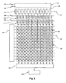
- the in Fig. 1 to 3 The image sensor shown can be used in both still and motion picture cameras, and has a plurality of photosensitive pixels 101 arranged in lines (shown horizontally here) and in columns (shown vertically here).
- the pixels 101 of each column are connected to a respective column line 103. All pixels of a row are connected to a respective row line 102.
- a row select circuit 104 allows the selection of a particular row line 102 so that all pixels of the respective row over the respective column lines 103 are connected to a respective signal preprocessor which in particular comprises column amplifiers.
- the signal preprocessing means present for each column line 103 are not shown individually here, but are part of a signal preprocessing unit 105, which in addition may also comprise sample-hold elements and / or analog-to-digital converters for digitizing the signals generated by the column amplifiers.
- the column lines 103 can each be connected via first switches 110 to a first test signal line 106.
- the column lines 103 can each be connected via second switches 111 to a second test signal line 107.
- Test input signals can be applied to the column lines 103 via the first test signal line 106 and the second test signal line 107.
- the signal pre-processing means of the signal preprocessing unit 105 are adapted to process not only the electrical signals (i.e., the wanted signals) generated by the pixels 101 and connected to the respective column line 103, but also the said test input signals.
- the three embodiments differ essentially by the control of the switches 110, 111, which will be explained in more detail below.
- the signal preprocessing unit 105 has a common output of the signal preprocessing devices, to which an evaluation unit 120 for the evaluation of the test input signals is connected.
- a first control line 108 for jointly controlling the first switches 110 and a second control line 109 for jointly controlling the second switches 111 are provided.
- a control signal to apply the test signals, either the first or the second control line 108 or 109 is supplied with a control signal.
- a first voltage source is applied to the first test signal line 106 and a second voltage source is applied to the second test signal line 107.
- the voltage sources may be both internal voltage sources integrated on the image sensor and external voltage sources.
- the first voltage source supplies a voltage of 2 V and the second voltage source supplies a voltage of 1.5 V.
- the regulation of the voltage sources must be designed so that the test voltages are stable and low-noise even under load.
- the first switches 110 are actuated, so that now the first voltage source with a voltage of 2 V is applied to the column lines 103. Subsequently, the image sensor is read so that the voltage of 2 V is read as a reference value in the respective signal preprocessing and buffered.
- connection of the column line 103 is interrupted with the first test signal line and by actuation of the second switch 111 by means of the second control line 109 connects to the second voltage source (1.5 V).
- This voltage is read into the respective signal preprocessing devices as a signal value and buffered.
- the voltage of 2 V corresponds to a reference value and the voltage of 1.5 V corresponds to a signal value.
- a test difference signal corresponding to the difference (0.5 V) of the two test input signals is produced at the output of the respective signal processing device (for example after amplification).
- the test difference signals generated in the individual signal preprocessing devices are digitized and output to the evaluation unit 120.
- a first test image can be generated, which corresponds to a bright input image.
- This first test image can be analyzed by the evaluation unit 120. For example, the digitized test difference signals can be compared with a predetermined reference value.
- the procedure described above is repeated, except that the first test voltage of 2 V is used for both the generation of the reference value and the signal value, that is, in the first passage.
- the column lines 103 are connected to the first test signal line 106 via the first switches 110. Due to the difference formation, the test difference signal in this case is 0 V, which is likewise digitized and output to the evaluation unit 120.
- the thus generated second test pattern corresponds to a black input image. This second test image can be analyzed separately in the evaluation unit 120 or compared with the first test image.
- test images By a line by line different control of the switches 110, 111 can be generated test images, which have horizontal lines.
- the 2V applied to the first test signal line 106 is used for both the reference value and the signal value, a test image is formed where every tenth line is bright, while all nine lines in between are dark.
- the second embodiment ( Fig. 2 ) differs from the first embodiment ( Fig. 1 ) in that the first and second switches 110, 111 are not driven via common control lines 108, 109, but that it can be separately selected for each column whether the associated column line 103 is to be connected to the first test signal line 106 or the second test signal line 107 , With others Words is the image sensor according to Fig. 2 adapted to considerablyrier the test input signals column by column variable on the column lines 103, ie without fixed pre-assignment, for example, due to a corresponding interconnection of associated transistors.
- a register 115 with a data input 113 is provided, via which data patterns can be loaded into the register 115.
- the size of the register 115 is determined by the column and row number of the image sensor.
- the data pattern stored in register 115 defines which of the two test signal lines 106, 107 should be connected to a specific column line 103.
- the register 115 thus serves as a control register.
- the register 115 has a number of register outputs 116 corresponding to the number of columns, the respective state of which can be determined by the data pattern and which are connected to a respective control logic 112.
- the control logics 112 are connected to a common control line 117. If a signal is present at this common control line 117, each control logic 112 actuates either a first switch 110 or a second switch 111 depending on the state of the associated register output 116.
- the register 115 also has a clock input 114, so that a different line of the data pattern is used to control the register outputs 116 for each test image line.
- corresponding data patterns in addition to test patterns with vertical stripe patterns, it is also possible to produce rectangular patterns or any other patterns.
- a register 115 can be used, which is designed only for storing single-line data patterns. After reading one or more lines with a particular data pattern, another data pattern can be loaded into the register 115 via the data input 113 so that test images with horizontal and vertical structures can also be generated with a single-line register.
- the third embodiment ( Fig. 3 ) largely corresponds to the second embodiment ( Fig. 2 ) and differs in that the control logics 112 are connected to two control lines 108, 109 instead of the common control line 117.
- Control line 108 Control line 109 Test signal line connected to the column lines 103: 0 0 no test signal line 1 0 first test signal line 106 0 1 second test signal line 107 1 1 Test signal line according to data pattern
- the feeding of the test voltages from the central test signal lines 106, 107 ensures in all embodiments that all column lines 103 connected to a respective test signal line 106, 107 are supplied with exactly the same test voltage. This avoids artifacts compared to solutions in which test signals are generated individually for each column and thus slightly differ from each other despite nominally the same voltage due to component tolerances.
- the switches 110, 111 ensure a direct, largely voltage-free and noise-free feeding of the test voltages into the column lines 103.
- a continuous monitoring of the image sensor in particular during regular operation of the camera can be done if one or two test images are generated in the manner described above between the reading of two useful signal images.
- the pixels of the image sensor can be deactivated.
- an automated evaluation of the test image (s) for the detection of defects or image defects can then take place, for example by an analysis by means of suitable methods on the basis of a Fourier analysis or a comparison with stored reference images.
- an optical or acoustic signal can be output to the operator of the camera.
Description
Die vorliegende Erfindung betrifft einen Bildsensor, insbesondere CMOS-Bildsensor, für elektronische Kameras, mit einer Vielzahl von in Zeilen und Spalten angeordneten lichtempfindlichen Pixeln, wobei alle oder zumindest ein Teil der Pixel einer Spalte mit einer jeweiligen gemeinsamen Spaltenleitung verbunden sind, und wobei der Bildsensor für eine oder mehrere der Spaltenleitungen eine jeweilige Signalvorverarbeitungseinrichtung aufweist, um von den Pixeln erzeugte und auf die jeweilige Spaltenleitung schaltbare Nutzsignale zu verarbeiten. Die Erfindung betrifft ferner eine Bildsensoreinheit.The present invention relates to an image sensor, in particular CMOS image sensor, for electronic cameras, comprising a plurality of photosensitive pixels arranged in rows and columns, wherein all or at least a part of the pixels of a column are connected to a respective common column line, and wherein the image sensor for one or more of the column lines has a respective signal preprocessing device to process generated by the pixels and switchable to the respective column line useful signals. The invention further relates to an image sensor unit.
Bekannte elektronische Kameras enthalten einen Bildsensor, der eine Vielzahl von in Zeilen und Spalten angeordneten lichtempfindlichen Elementen bzw. Pixel umfasst, welche durch ein Objektiv der Kamera fallendes Licht in elektrische Signale umwandeln. Zum Auslesen eines Bildes wird jedes der Pixel adressiert, und ein Signal, das zu einer durch eine Belichtung gesammelten Ladung des Pixels proportional ist, wird zu einem Ausgang des Bildsensors geleitet und in ein digitales Signal umgewandelt.Known electronic cameras include an image sensor comprising a plurality of light-sensitive elements or pixels arranged in rows and columns, which convert light falling through a lens of the camera into electrical signals. To read an image, each of the pixels is addressed, and a signal proportional to a charge of the pixel collected by an exposure is passed to an output of the image sensor and converted to a digital signal.
Zum Auslesen eines Bildes werden die Pixel zeilenweise mittels einer gemeinsamen Zeilenleitung adressiert und über am Ende der Spaltenleitungen angeordnete Signalvorverarbeitungseinrichtungen ausgegeben und mit Hilfe von auf dem Sensor vorhandener oder externer Analog-DigitalWandler digitalisiert.To read out an image, the pixels are addressed line by line by means of a common row line and output via arranged at the end of the column lines signal preprocessing and digitized using existing on the sensor or external analog-to-digital converter.
Üblicherweise werden zur Reduzierung des Einflusses unterschiedlicher Offset-Pegel der Pixel, auch als Fixed Pattern Noise (FPN) bezeichnet, zwei Werte aus jedem Pixel ausgelesen, nämlich ein Signalwert, welcher bei belichtetem Pixel erzeugt wird, und ein Referenzwert, welcher bei unbelichtetem und zurückgesetztem Pixel erzeugt wird und ein Offset-Signal darstellt. Signalwert und Referenzwert werden einem Differenzverstärker zugeführt, welcher Bestandteil der Signalvorverarbeitungseinrichtung ist. Das eigentliche Bildsignal wird aus der Differenz von Signal- und Referenzwert gewonnen und kann anschließend weiterverarbeitet werden. Ein derartiges Verfahren wird auch als Correlated-Double-Sampling (CDS) bezeichnet.Typically, to reduce the influence of different offset levels of the pixels, also referred to as fixed pattern noise (FPN), two values are read out of each pixel, namely a signal value generated when the pixel is exposed, and a reference value which is unexposed and reset Pixel is generated and represents an offset signal. Signal value and reference value are fed to a differential amplifier, which is part of the signal preprocessing device. The actual image signal is obtained from the difference between signal and reference value and can then be further processed. Such a method is also referred to as Correlated Double Sampling (CDS).
Elektronische Kameras werden heute zunehmend bei der Produktion von Kinofilmen eingesetzt. Bei dieser Anwendung treten regelmäßig sehr hohe Kosten für Schauspieler und die Produktionsmitarbeiter auf. Daher ist es besonders wichtig, dass die eingesetzten Kameras fehlerfrei funktionieren.Electronic cameras are increasingly used today in the production of motion picture films. In this application, very high costs for actors and the production staff regularly occur. It is therefore particularly important that the cameras used work flawlessly.
Bei defekten elektronischen Kameras sind vor allem solche Fehler besonders nachteilig, die nicht sofort erkannt werden. Während ein Totalausfall einer elektronischen Kamera ohne weiteres erkennbar ist und die betreffende Kamera ausgetauscht wird, bleiben Fehler, die nur geringfügige Bildstörungen verursachen und z.B. auf Verschmutzung des Sensors, Veränderung der Kennlinien von elektronischen Bauteilen oder erhöhtes Rauschen zurückzuführen sind, möglicherweise zunächst unerkannt.In the case of defective electronic cameras, especially those errors that are not recognized immediately are particularly disadvantageous. While a total failure of an electronic camera is readily apparent and the camera in question is replaced, errors that cause only minor image disturbances and e.g. due to contamination of the sensor, changes in the characteristics of electronic components or increased noise, may initially be unrecognized.
Dennoch können derartige Bildstörungen bei einer Projektion des Kinofilms auf einer großen Leinwand deutlich sichtbar werden und durch nachträgliche, bei der Postproduktion vorgenommene Bildkorrekturen sogar noch verstärkt werden.Nevertheless, when the movie is projected onto a large screen, such image disturbances can become clearly visible and even exacerbated by post-production image corrections.
Beim Auftreten von Bildstörungen müssen die betroffenen Bilder aufwendig manuell retuschiert werden. Im schlimmsten Fall muss die Filmaufnahme wiederholt werden, was mit erheblichen Mehrkosten verbunden ist.If image interference occurs, the affected images must be manually retouched. In the worst case, the film recording must be repeated, which is associated with significant additional costs.
Gewöhnlich wird die korrekte Funktion einer elektronischen Kamera verifiziert, indem mit der Kamera definierte Vorlagen abgefilmt werden. Diese enthalten typischerweise verschiedene kalibrierte Farbtafeln, Vorlagen mit hohem Kontrastumfang sowie homogen ausgeleuchtete Flächen. Beispielsweise wird eine Ulbricht-Kugel mit großformatigen Vorlagen verwendet, die in einem abgedunkelten Raum abgefilmt wird.Usually, the correct function of an electronic camera is verified by filmed with the camera defined templates. These typically contain a variety of calibrated color charts, high-contrast originals, and homogeneously illuminated areas. For example, an Ulbricht sphere with large format templates is used, which is filmed in a darkened room.
Eine derartige Ausrüstung ist jedoch häufig zu sperrig, um sie am Drehort zu verwenden. Zudem ist für die Auswertung der aufgenommenen Testdaten eine spezielle Analysesoftware nötig, die für ihren Betrieb das Vorhandensein eines Computers und besonderes Fachwissen der Bedienperson erfordert.However, such equipment is often too bulky to use at the location of shooting. In addition, a special analysis software is required for the evaluation of the recorded test data, which requires for their operation the presence of a computer and special expertise of the operator.
Dokument
Dokument
Es ist die Aufgabe der Erfindung, einen Bildsensor und eine Bildsensoreinheit anzugeben, welche eine Funktionsüberwachung einer elektronischen Kamera insbesondere im laufenden Betrieb ermöglichen.It is the object of the invention to provide an image sensor and an image sensor unit, which enable a functional monitoring of an electronic camera, in particular during operation.
Diese Aufgabe wird durch einen Bildsensor mit den Merkmalen des Anspruchs 1 gelöst und insbesondere durch einen Bildsensor, insbesondere CMOS-Bildsensor, für elektronische Kameras mit einer Vielzahl von in Zeilen und Spalten angeordneten lichtempfindlichen Pixeln, wobei alle oder zumindest ein Teil der Pixel einer Spalte mit einer jeweiligen gemeinsamen Spaltenleitung verbunden sind, und wobei der Bildsensor für eine oder mehrere der Spaltenleitungen eine jeweilige Signalvorverarbeitungseinrichtung aufweist, um von den Pixeln erzeugte und auf die jeweilige Spaltenleitung schaltbare Nutzsignale zu verarbeiten. Der Bildsensor ist dazu ausgebildet, wahlweise eines von zumindest zwei Testeingangssignalen auf die Spaltenleitungen aufzuschalten, wobei der Bildsensor zumindest eine erste und eine zweite Spannungsquelle zur Erzeugung der Testeingangssignale aufweist, und wobei die jeweilige Spannungsquelle eine unabhängig von der Versorgungsspannung des Bildsensors geregelte Spannungsquelle ist.This object is achieved by an image sensor with the features of claim 1 and in particular by an image sensor, in particular CMOS image sensor, for electronic cameras with a plurality of arranged in rows and columns photosensitive pixels, all or at least a portion of the pixels of a column a respective common column line are connected, and wherein the image sensor for one or more of the column lines has a respective signal preprocessing means for processing useful signals generated by the pixels and switchable to the respective column line. The image sensor is configured to selectively connect one of at least two test input signals to the column lines, the image sensor having at least one first and one second voltage source for generating the test input signals, and wherein the respective voltage source is a voltage source regulated independently of the supply voltage of the image sensor.
Durch das Aufschalten der Testeingangssignale kann für jedes Pixel eine durch die Größe der Testeingangssignale vorgegebene Simulation bestimmter Belichtungssituationen erreicht werden. Es werden hierbei definierte Ausgangssignale der Pixel nachgebildet. Dadurch kann überprüft werden, ob Defekte oder Unregelmäßigkeiten zum Beispiel im Bereich der sensorinternen Leitungen, beispielsweise der Spaltenleitungen, oder im Bereich der nachfolgenden Signalvorverarbeitung vorliegen, etwa bei einzelnen Verstärkern, Abtast-Halte-Gliedern oder Analog-Digital-Wandlern.By switching on the test input signals, a simulation of specific exposure situations predetermined by the size of the test input signals can be achieved for each pixel. In this case, defined output signals of the pixels are reproduced. This makes it possible to check whether defects or irregularities are present, for example, in the region of the sensor-internal lines, for example the column lines, or in the area of the subsequent signal preprocessing, for example with individual amplifiers, sample-and-hold elements or analog-to-digital converters.
Vorzugsweise ist der Bildsensor dazu ausgebildet, die Testeingangssignale ohne wesentlichen Spannungsabfall auf die Spaltenleitungen aufzuschalten, d.h. das Aufschalten der Testeingangssignale auf die Spaltenleitungen erfolgt mittels entsprechend konfigurierter Schalter unmittelbar ohne wesentlichen Spannungsabfall. Hierdurch werden unerwünschte Rauschquellen und durch Fertigungstoleranzen bedingte Abweichungen der tatsächlich eingespeisten Testeingangssignale zwischen den verschiedenen Spaltenleitungen vermieden. Mit anderen Worten wird durch die Verwendung von Schaltern, die eine Übertragung der Testeingangssignale ohne Spannungsabfall ermöglichen, gewährleistet, dass an den verschiedenen Spaltenleitungen dasselbe jeweilige Testeingangssignal anliegt. Hierdurch sind genauere Messungen möglich. Insbesondere ist es hierfür bevorzugt, wenn die Testeingangssignale nicht um die jeweilige Gate-Source-Spannung eines zwischengeschalteten Transistors vermindert werden.Preferably, the image sensor is adapted to aufzuschalten the test input signals without significant voltage drop on the column lines, ie the connection of the test input signals on the column lines by means of appropriately configured switches immediately without significant voltage drop. This causes unwanted noise sources and caused by manufacturing tolerances deviations of the actually fed test input signals between the different column lines avoided. In other words, the use of switches that enable transmission of the test input signals without a voltage drop ensures that the same respective test input signal is applied to the different column lines. As a result, more accurate measurements are possible. In particular, it is preferred for this purpose if the test input signals are not reduced by the respective gate-source voltage of an interconnected transistor.
Um besonders genaue Messergebnisse zu erhalten, ist die zur Erzeugung der Testeingangssignale verwendete jeweilige Spannungsquelle eine unabhängig von der Versorgungsspannung des Bildsensors geregelte Spannungsquelle.In order to obtain particularly accurate measurement results, the respective voltage source used to generate the test input signals is an independent of the supply voltage of the image sensor voltage source.
Gemäß einer bevorzugten Ausführungsform ist jede Spaltenleitung derart mit einem jeweiligen ersten Schalter und einem jeweiligen zweiten Schalter verbunden, dass die jeweilige Spaltenleitung über den ersten Schalter und den zweiten Schalter wahlweise mit zumindest einer ersten Testsignalleitung oder einer zweiten Testsignalleitung verbunden werden kann. Dadurch kann auf einfache Weise eine Zuordnung verschiedener Testeingangssignale zu den Spaltenleitungen erreicht werden.According to a preferred embodiment, each column line is connected to a respective first switch and a respective second switch such that the respective column line can be selectively connected to at least a first test signal line or a second test signal line via the first switch and the second switch. As a result, an assignment of different test input signals to the column lines can be achieved in a simple manner.
Gemäß einer bevorzugten Ausführungsform sind die ersten Schalter mit einer ersten Steuerleitung zur gemeinsamen Ansteuerung der ersten Schalter verbunden und die zweiten Schalter mit einer zweiten Steuerleitung zur gemeinsamen Ansteuerung der zweiten Schalter verbunden. Mit dieser Anordnung kann zu einem bestimmten Zeitpunkt auf jede Spaltenleitung das gleiche Testeingangssignal aufgeschaltet werden.According to a preferred embodiment, the first switches are connected to a first control line for the common activation of the first switches and the second switches are connected to a second control line for the common activation of the second switches. With this arrangement, the same test input signal can be applied to each column line at a certain time.
Gemäß einer weiteren Ausführungsform der Erfindung sind die Spaltenleitungen mit verschiedenen Testsignalleitungen verbindbar. Dadurch ist es beispielsweise möglich, in einem Testbild vertikale Linien oder Streifenmuster zu erzeugen.According to a further embodiment of the invention, the column lines can be connected to different test signal lines. This makes it possible, for example, to generate vertical lines or stripe patterns in a test pattern.
Vertikale Streifenmuster sind insbesondere wichtig, um Echos oder Geisterbilder erkennen zu können. So werden bei Kameras, die gleichzeitig eine hohe Anzahl von lichtempfindlichen Elementen oder eine hohe Bildrate besitzen, Bildsensoren verwendet, die mehrere Ausgänge A aufweisen, welche in einem jeweiligen Auslesezyklus parallel - und somit schneller - ausgelesen werden können. Zusätzlich können die Spalten in Spaltengruppen eingeteilt sein, welche jeweils mehrere Spalten aufweisen, wobei die Anzahl der Spalten in einer jeden der Spaltengruppen der Anzahl der Ausgänge A entspricht. Dabei sind die Spalten den Ausgängen des Bildsensors nach Art nebeneinander liegender Einheitsmatrizen zugeordnet, so dass die Spalten mit den Nummern N, N+A, N+2A usw. jeweils dem Ausgang mit der Nummer N zugeordnet sind, wobei die Spalten und die Ausgänge jeweils fortlaufend nummeriert sind.Vertical striped patterns are particularly important for detecting echoes or ghosting. Thus, in cameras which simultaneously have a high number of photosensitive elements or a high frame rate, image sensors are used which have a plurality of outputs A, which in a respective read cycle parallel - and thus faster - can be read out. In addition, the columns may be divided into column groups each having a plurality of columns, the number of columns in each of the column groups corresponding to the number of outputs A. In this case, the columns are assigned to the outputs of the image sensor in the manner of juxtaposed unitary matrices, so that the columns with the numbers N, N + A, N + 2A, etc. are each assigned to the output with the number N, the columns and the outputs respectively consecutively numbered.
So ist beispielsweise bei einem Bildsensor mit 32 Ausgängen und mit einer Unterteilung der Spalten in Spaltengruppen in einem ersten Auslösezyklus die erste Spalte des Bildsensors, welche der ersten Spalte der ersten Spaltengruppe entspricht, dem ersten Ausgang zugeordnet. Die zweite Spalte des Bildsensors, welche der zweiten Spalte der ersten Spaltengruppe entspricht, ist dem zweiten Ausgang zugeordnet usw. bis zu der 32. Spalte des Bildsensors, welche der 32. Spalte der ersten Spaltengruppe entspricht, die dem 32. Ausgang zugeordnet ist. In dem nachfolgenden Auslesezyklus ist die 33. Spalte des Bildsensors, welche der ersten Spalte der zweiten Spaltengruppe entspricht, wieder dem ersten Ausgang zugeordnet, die 34. Spalte des Bildsensors, welche der zweiten Spalte der zweiten Spaltengruppe entspricht, wieder dem zweiten Ausgang zugeordnet USW.For example, in an image sensor with 32 outputs and with a subdivision of the columns in column groups in a first trip cycle, the first column of the image sensor, which corresponds to the first column of the first column group, associated with the first output. The second column of the image sensor corresponding to the second column of the first column group is associated with the second output and so on up to the 32nd column of the image sensor corresponding to the 32nd column of the first column group associated with the 32nd output. In the subsequent read cycle, the 33rd column of the image sensor, which corresponds to the first column of the second column group, is again assigned to the first output, the 34th column of the image sensor, which corresponds to the second column of the second column group, again assigned to the second output USW.
Jeder der Ausgänge des Bildsensors weist einen eigenen Ausgangsverstärker auf, wobei durch die Ausgangsverstärker die Signale der Pixel verstärkt werden, um anschließend digitalisiert zu werden.Each of the outputs of the image sensor has its own output amplifier, whereby the output amplifiers amplify the signals of the pixels for subsequent digitization.
Es ist bekannt, dass das jeweils aktuell an einem Ausgangsverstärker anliegende Signal immer einen kleinen, beispielsweise im Promillebereich liegenden Anteil des durch den jeweiligen Ausgangsverstärker unmittelbar zuvor verstärkten Signals enthält, welcher Anteil beispielsweise durch thermische Effekte und/oder Rückwirkungen auf die Spannungsversorgung verursacht wird. Während der störende Einfluss des Signals des Vorgängerpixels bei einem Bildsensor mit einem einzigen Ausgang bei großen Unterschieden zwischen zwei unmittelbar nacheinander verstärkten Signalen zwar eine Art Unschärfe im Bild erzeugt, die mit dem Auge nicht wahrnehmbar ist, macht sich bei einem Bildsensor mit mehreren Ausgängen der Anteil des Signals des jeweiligen Vorgängerpixels - also der Anteil des unmittelbar zuvor verstärkten Signals - bei der Verstärkung des Signals desjenigen Pixels bemerkbar, das um die Anzahl der Ausgänge A von dem Vorgängerpixel entfernt angeordnet ist.It is known that the respective signal currently present at an output amplifier always has a small proportion, for example, in the per thousand range, of the signal directly through the respective output amplifier previously amplified signal contains, which proportion is caused for example by thermal effects and / or effects on the power supply. While the disturbing influence of the signal of the predecessor pixel in a single-output image sensor with large differences between two immediately successively amplified signals generates a kind of blurring in the image that is imperceptible to the eye, in a multi-output image sensor the proportion is increased the signal of the respective predecessor pixel - that is, the proportion of the immediately previously amplified signal - noticeable in the amplification of the signal of that pixel, which is located by the number of outputs A from the predecessor pixel.
Beispielsweise wird so in einem Bild, welches eine helle Kerzenflamme in einem ansonsten dunklen Raum zeigt, ein visuelles Echo der Kerzenflamme erzeugt, welches seitlich zu der Original-Kerzenflamme versetzt ist. Eine derartige echoartige Bildstörung wird als Geisterbild bezeichnet. So ist bei dem vorstehend beschriebenen Bildsensor mit 32 Ausgängen das Echo um 32 Pixel von dem Original versetzt.For example, in an image showing a bright candle flame in an otherwise dark room, a visual echo of the candle flame is generated which is laterally offset from the original candle flame. Such an echo-like picture disturbance is called ghosting. Thus, in the 32-output image sensor described above, the echo is offset 32 pixels from the original.
Mit Hilfe der vorliegenden Erfindung können nun beliebige vertikale Streifenmuster erzeugt werden, mit denen derartige Störungen in der Signalverarbeitungskette erkannt werden können.With the aid of the present invention, any vertical stripe patterns can now be generated with which such disturbances in the signal processing chain can be detected.
Für eine Verbindung der Spaltenleitungen mit verschiedenen Testsignalleitungen kann ein Register vorgesehen sein, welches ausgebildet ist, die ersten und zweiten Schalter für jede Spaltenleitung separat anzusteuern, so dass die jeweilige Spaltenleitung wahlweise mit der ersten Testsignalleitung, der zweiten Testsignalleitung oder keiner Testsignalleitung verbunden ist. In dem Register kann ein Muster abgelegt werden, welches die Aufschaltung der Testeingangssignale steuert. Dieses Muster kann statisch, d.h. für alle Zeilen gleich oder auch zeilenweise unterschiedlich oder veränderbar sein.For a connection of the column lines to different test signal lines, a register may be provided which is designed to separately control the first and second switches for each column line so that the respective column line is selectively connected to the first test signal line, the second test signal line or no test signal line. In the register, a pattern can be stored, which controls the connection of the test input signals. This pattern can be static, ie be the same for all lines or line by line different or changeable.
Ferner kann der Bildsensor wenigstens eine Auswerteeinrichtung aufweisen, die mit einem gemeinsamen Ausgang der Signalvorverarbeitungseinrichtungen verbunden ist, wobei die Auswerteeinrichtung dazu ausgebildet ist, die Testeingangssignale nach deren Verarbeitung in den Signalvorverarbeitungseinrichtungen auszuwerten. Hierdurch können die so erzeugten Testdifferenzsignale oder Testbilder zeitnah, insbesondere während des laufenden Betriebs, ausgewertet werden. Durch die Unterbringung auf dem Sensor wird eine Platz sparende Bauweise erreicht, und eine Verfälschung der Testsignale durch große Leitungslängen wird vermieden.Furthermore, the image sensor can have at least one evaluation device, which is connected to a common output of the signal preprocessing devices, wherein the evaluation device is designed to evaluate the test input signals after their processing in the signal preprocessing devices. As a result, the test difference signals or test images generated in this way can be evaluated in a timely manner, in particular during ongoing operation. By accommodating on the sensor space-saving design is achieved, and a falsification of the test signals by long line lengths is avoided.
Der Bildsensor kann auch dazu ausgebildet sein, wahlweise eines von mehr als zwei Testeingangssignalen (z.B. eines von vier Testeingangssignalen) auf die Spaltenleitungen aufzuschalten. In diesem Fall ist vorzugsweise eine entsprechende Anzahl von Schaltern, Testsignalleitungen und/oder Spannungsquellen vorgesehen.The image sensor may also be configured to selectively connect one of more than two test input signals (e.g., one of four test input signals) to the column lines. In this case, a corresponding number of switches, test signal lines and / or voltage sources is preferably provided.
Die Aufgabe der Erfindung wird ferner durch eine Bildsensoreinheit mit den Merkmalen des Anspruchs 12 gelöst. Eine derartige Bildsensoreinheit umfasst einen Bildsensor der vorstehend erläuterten Art und zumindest eine erste externe Spannungsquelle und eine zweite externe Spannungsquelle zur Erzeugung der genannten Testeingangssignale, wobei die externen Spannungsquellen mit zugeordneten Anschlüssen des Bildsensors verbunden sind, und wobei die jeweilige externe Spannungsquelle eine unab- hängig von der Versorgungsspannung des Bildsensors geregelte Spannungsquelle ist.The object of the invention is further achieved by an image sensor unit having the features of claim 12. Such an image sensor unit comprises an image sensor of the type described above and at least a first external voltage source and a second external voltage source for generating said test input signals, wherein the external voltage sources are connected to associated terminals of the image sensor, and wherein the respective external voltage source is an independent is dependent on the supply voltage of the image sensor regulated voltage source.
Weitere vorteilhafte Ausgestaltungen der Erfindung sind in den Unteransprüchen, der Beschreibung und der Zeichnung angegeben.Further advantageous embodiments of the invention are specified in the subclaims, the description and the drawing.
Die Erfindung wird nachfolgend anhand von Ausführungsbeispielen mit Bezug auf die Zeichnung beschrieben.The invention will now be described by way of example with reference to the drawings.
Es zeigen, jeweils in schematischer Darstellung:
- Fig. 1
- eine erste Ausführungsform eines erfindungsgemäßen Bildsensors,
- Fig. 2
- eine zweite Ausführungsform eines erfindungsgemäßen Bildsensors, und
- Fig. 3
- eine dritte Ausführungsform eines erfindungsgemäßen Bildsensors.
- Fig. 1
- A first embodiment of an image sensor according to the invention,
- Fig. 2
- a second embodiment of an image sensor according to the invention, and
- Fig. 3
- A third embodiment of an image sensor according to the invention.
Der in
Die für jede Spaltenleitung 103 vorhandenen Signalvorverarbeitungseinrichtungen sind hier nicht einzeln dargestellt, sondern Bestandteil einer Signalvorverarbeitungseinheit 105, welche darüber hinaus auch Abtast-Halte-Glieder und/oder Analog-Digital-Wandler zur Digitalisierung der von den Spaltenverstärkern erzeugten Signale umfassen kann.The signal preprocessing means present for each
Die Spaltenleitungen 103 sind jeweils über erste Schalter 110 mit einer ersten Testsignalleitung 106 verbindbar. Darüber hinaus sind die Spaltenleitungen 103 jeweils über zweite Schalter 111 mit einer zweiten Testsignalleitung 107 verbindbar. Über die erste Testsignalleitung 106 und die zweite Testsignalleitung 107 können Testeingangssignale auf die Spaltenleitungen 103 aufgeschaltet werden. Die Signalvorverarbeitungseinrichtungen der Signalvorverarbeitungseinheit 105 sind dazu ausgebildet, nicht nur die von den Pixeln 101 erzeugten und auf die jeweilige Spaltenleitung 103 geschalteten elektrischen Signale (d.h. die Nutzsignale) zu verarbeiten, sondern auch die genannten Testeingangssignale.The column lines 103 can each be connected via
Die drei Ausführungsbeispiele unterscheiden sich im Wesentlichen durch die Ansteuerung der Schalter 110, 111, welche nachfolgend noch näher erläutert wird.The three embodiments differ essentially by the control of the
Die Signalvorverarbeitungseinheit 105 weist einen gemeinsamen Ausgang der Signalvorverarbeitungseinrichtungen auf, an dem eine Auswerteeinheit 120 zur Auswertung der Testeingangssignale angeschlossen ist.The
Obwohl für den hier dargestellten Bildsensor nur eine einzige Signalvorverarbeitungseinheit 105 dargestellt ist, ist es selbstverständlich auch möglich, in bekannter Weise anstelle einer einzigen Signalvorverarbeitungseinheit mehrere parallel arbeitende Signalvorverarbeitungseinheiten vorzusehen, um ein schnelleres Auslesen des Bildsensors zu ermöglichen. Entsprechend sind dann die gemeinsamen Ausgänge der mehreren Signalvorverarbeitungseinheiten mit der Auswerteeinheit 120 verbunden.Although only a single
Nachfolgend wird nun der Betrieb des erfindungsgemäßen Bildsensors gemäß dem ersten Ausführungsbeispiel beschrieben.The operation of the image sensor according to the invention according to the first embodiment will now be described below.
Bei dem ersten Ausführungsbeispiel gemäß
Wie eingangs erwähnt wurde, werden beim CDS-Verfahren aus jedem Pixel zwei Werte ausgelesen, nämlich ein Signalwert und ein Referenzwert. Die Differenz dieser beiden Werte wird dann verstärkt und in einem Analog-Digital-Wandler digitalisiert. Demnach müssen auch zwei entsprechende Testsignalwerte bereitgestellt werden.As mentioned in the beginning, two values are read from each pixel in the CDS method, namely a signal value and a reference value. The difference between these two values is then amplified and digitized in an analog-to-digital converter. Accordingly, two corresponding test signal values must also be provided.
Zur Durchführung einer beispielhaften Bildsensorüberprüfung wird eine erste Spannungsquelle an die erste Testsignalleitung 106 und eine zweite Spannungsquelle an die zweite Testsignalleitung 107 angelegt. Bei den nicht dargestellten Spannungsquellen kann es sich sowohl um interne, auf dem Bildsensor integrierte Spannungsquellen als auch um externe Spannungsquellen handeln. Beispielsweise liefert die erste Spannungsquelle eine Spannung von 2 V und die zweite Spannungsquelle eine Spannung von 1,5 V. Die Regelung der Spannungsquellen ist so auszulegen, dass die Testspannungen auch unter Last stabil und rauscharm sind.To perform an exemplary image sensor check, a first voltage source is applied to the first
Durch entsprechende Ansteuerung über die erste Steuerleitung 108 werden die ersten Schalter 110 betätigt, so dass nun die erste Spannungsquelle mit einer Spannung von 2 V an den Spaltenleitungen 103 anliegt. Nachfolgend wird der Bildsensor so ausgelesen, dass die Spannung von 2 V als Referenzwert in die jeweiligen Signalvorverarbeitungseinrichtungen eingelesen und zwischengespeichert wird.By appropriate control via the
Anschließend wird die Verbindung der Spaltenleitung 103 mit der ersten Testsignalleitung unterbrochen und durch eine Betätigung der zweiten Schalter 111 mittels der zweiten Steuerleitung 109 eine Verbindung mit der zweiten Spannungsquelle (1,5 V) hergestellt. Diese Spannung wird in die jeweiligen Signalvorverarbeitungseinrichtungen als Signalwert eingelesen und zwischengespeichert.Subsequently, the connection of the
Hier entspricht also die Spannung von 2 V einem Referenzwert und die Spannung von 1,5 V einem Signalwert. Aus der Differenz dieser beiden Werte ergibt sich am Ausgang der jeweiligen Signalverarbeitungseinrichtung (z.B. nach Verstärkung) ein Testdifferenzsignal, das der Differenz (0,5 V) der beiden Testeingangssignale entspricht. Die in den einzelnen Signalvorverarbeitungseinrichtungen erzeugten Testdifferenzsignale werden digitalisiert und an die Auswerteeinheit 120 ausgegeben.Here, therefore, the voltage of 2 V corresponds to a reference value and the voltage of 1.5 V corresponds to a signal value. From the difference between these two values, a test difference signal corresponding to the difference (0.5 V) of the two test input signals is produced at the output of the respective signal processing device (for example after amplification). The test difference signals generated in the individual signal preprocessing devices are digitized and output to the
Diese Schritte werden entsprechend der Zeilenanzahl des Bildsensors wiederholt, so dass letztlich aus den Testdifferenzsignalen ein erstes Testbild erzeugt werden kann, das einem hellen Eingangsbild entspricht. Dieses erste Testbild kann von der Auswerteeinheit 120 analysiert werden. Beispielsweise können die digitalisierten Testdifferenzsignale mit einem vorgegebenen Referenzwert verglichen werden.These steps are repeated according to the number of lines of the image sensor, so that ultimately from the test difference signals, a first test image can be generated, which corresponds to a bright input image. This first test image can be analyzed by the
Vorzugsweise wird der vorstehend beschriebene Vorgang wiederholt, wobei in Abweichung vom ersten Durchgang die erste Testspannung von 2 V sowohl für die Erzeugung des Referenzwerts als auch des Signalwerts verwendet wird, d.h. die Spaltenleitungen 103 sind in beiden Fällen über die ersten Schalter 110 mit der ersten Testsignalleitung 106 verbunden. Aufgrund der Differenzbildung beträgt das Testdifferenzsignal in diesem Fall 0 V, welches ebenfalls digitalisiert und an die Auswerteeinheit 120 ausgegeben wird. Das derart erzeugte zweite Testbild entspricht einem schwarzen Eingangsbild. Dieses zweite Testbild kann in der Auswerteeinheit 120 separat analysiert werden oder mit dem ersten Testbild verglichen werden.Preferably, the procedure described above is repeated, except that the first test voltage of 2 V is used for both the generation of the reference value and the signal value, that is, in the first passage. In both cases, the column lines 103 are connected to the first
Durch eine zeilenweise unterschiedliche Ansteuerung der Schalter 110, 111 lassen sich Testbilder erzeugen, welche horizontale Linien aufweisen. Wenn also eine Testbildzeile mit einem Referenzwert von 2 V und einem Signalwert von 1,5 V erzeugt, während bei den nachfolgenden neun Testbildzeilen die an der ersten Testsignalleitung 106 anliegenden 2 V sowohl für den Referenzwert als auch für den Signalwert verwendet werden, entsteht ein Testbild, bei dem jede zehnte Zeile hell ist, während alle dazwischen liegenden neun Zeilen dunkel sind.By a line by line different control of the
Das zweite Ausführungsbeispiel (
Dazu ist ein Register 115 mit einem Dateneingang 113 vorgesehen, über den Datenmuster in das Register 115 geladen werden können. Die Größe des Registers 115 bestimmt sich aus der Spalten- und Zeilenanzahl des Bildsensors. Das im Register 115 abgelegte Datenmuster definiert, welche der beiden Testsignalleitungen 106, 107 mit einer bestimmten Spaltenleitung 103 verbunden werden soll. Das Register 115 dient also als Steuerregister.For this purpose, a
Das Register 115 weist eine der Spaltenzahl entsprechende Anzahl von Registerausgängen 116 auf, deren jeweiliger Zustand durch das Datenmuster bestimmbar ist und die mit einer jeweiligen Steuerlogik 112 verbunden sind. Die Steuerlogiken 112 sind mit einer gemeinsamen Steuerleitung 117 verbunden. Liegt nun an dieser gemeinsamen Steuerleitung 117 ein Signal an, betätigt jede Steuerlogik 112 in Abhängigkeit von dem Zustand des zugeordneten Registerausgangs 116 entweder einen ersten Schalter 110 oder einen zweiten Schalter 111.The
Das Register 115 verfügt ferner über einen Takteingang 114, so dass für jede Testbildzeile eine andere Zeile des Datenmusters zur Ansteuerung der Registerausgänge 116 herangezogen wird. Durch entsprechende Datenmuster lassen sich neben Testbildern mit vertikalen Streifenmustern auch rechteckförmige Muster oder beliebige andere Muster erzeugen.The
Alternativ kann auch ein Register 115 verwendet werden, das nur zur Speicherung einzeiliger Datenmuster ausgelegt ist. Nach dem Auslesen einer oder mehrerer Zeilen mit einem bestimmten Datenmuster kann ein anderes Datenmuster über den Dateneingang 113 in das Register 115 geladen werden, sodass auch mit einem einzeiligen Register Testbilder mit horizontalen und vertikalen Strukturen erzeugt werden können.Alternatively, a
Das dritte Ausführungsbeispiel (
Dazu erfolgt eine entsprechende Auswertung der Zustände der beiden Steuerleitungen 108, 109 in den Steuerlogiken 112. Zum Beispiel kann die Codierung gemäß nachstehender Tabelle erfolgen:
Die Einspeisung der Testspannungen aus den zentralen Testsignalleitungen 106, 107 stellt bei allen Ausführungsformen sicher, dass alle mit einer jeweiligen Testsignalleitung 106, 107 verbundenen Spaltenleitungen 103 mit genau derselben Testspannung beaufschlagt werden. Damit werden Artefakte gegenüber Lösungen vermieden, bei denen Testsignale individuell für jede Spalte erzeugt werden und somit trotz nominell gleicher Spannung aufgrund von Bauteiltoleranzen geringfügig voneinander abweichen. Die Schalter 110, 111 gewährleisten eine direkte, weitgehend spannungsabfallfreie und rauschfreie Einspeisung der Testspannungen in die Spaltenleitungen 103.The feeding of the test voltages from the central
Bei allen Ausführungsbeispielen kann eine fortlaufende Überwachung des Bildsensors insbesondere während des regulären Betriebs der Kamera erfolgen, wenn zwischen dem Auslesen von zwei Nutzsignal-Bildern ein oder zwei Testbilder auf die vorstehend beschriebene Weise erzeugt werden. Während des Auslesens der Testbilder können die Pixel des Bildsensors deaktiviert werden.In all embodiments, a continuous monitoring of the image sensor, in particular during regular operation of the camera can be done if one or two test images are generated in the manner described above between the reading of two useful signal images. During the reading out of the test images, the pixels of the image sensor can be deactivated.
In der Auswerteeinheit 120 kann dann eine automatisierte Auswertung des oder der Testbilder zur Erkennung von Defekten oder Bildfehlern erfolgen, beispielsweise durch eine Analyse mittels geeigneter Verfahren auf der Grundlage einer Fourier-Analyse oder einem Vergleich mit abgespeicherten Referenzbildern.In the
Bei einer Erkennung von Defekten oder Bildfehlern kann ein optisches oder akustisches Signal an die Bedienperson der Kamera ausgegeben werden.Upon detection of defects or image defects, an optical or acoustic signal can be output to the operator of the camera.
Analog zu der Verwendung von zwei Testspannungen ist es bei den vorstehend erläuterten Ausführungsbeispielen natürlich auch möglich, mehr als zwei Testspannungen zu verwenden, d.h. mehr als zwei Testspannungen wahlweise auf die Spaltenleitungen 103 aufzuschalten. Wenn beispielsweise vier Testspannungen verwendet werden, so werden in dem Register 115 gemäß
- 101101
- Pixelpixel
- 102102
- Zeilenleitungrow line
- 103103
- Spaltenleitungcolumn line
- 104104
- ZeilenauswahlschaltungRow selection circuit
- 105105
- Signalvorverarbeitungseinheitsignal preprocessing
- 106106
- erste Testsignalleitungfirst test signal line
- 107107
- zweite Testsignalleitungsecond test signal line
- 108108
- erste Steuerleitungfirst control line
- 109109
- zweite Steuerleitungsecond control line
- 110110
- erster Schalterfirst switch
- 111111
- zweiter Schaltersecond switch
- 112112
- Steuerlogikcontrol logic
- 113113
- Dateneingangdata input
- 114114
- Takteingangclock input
- 115115
- Registerregister
- 116116
- Registerausgangregister output
- 117117
- gemeinsame Steuerleitungcommon control line
- 120120
- Auswerteeinheitevaluation
Claims (13)
- An image sensor, in particular a CMOS image sensor, for electronic cameras, having a plurality of light-sensitive pixels (101) arranged in rows and columns, wherein all or at least some of the pixels (101) of a column are connected to a respective common column line (103), wherein the image sensor has a respective signal preprocessing device (105) for one or more of the column lines (103) to process wanted signals which are generated by the pixels and which can be switched to the respective column line (103), wherein the image sensor is designed selectively to switch one of at least two test input signals to the column line (103), and wherein the image sensor has at least one first voltage source and one second voltage source for generating the test input signals,
characterised in that
the respective voltage source is a voltage source regulated independently of the supply voltage of the image sensor. - An image sensor in accordance with claim 1,
characterised in that
the image sensor is designed to switch the test input signals onto the column lines (103) without any voltage drop. - An image sensor in accordance with claim 1 or claim 2,
characterised in that
each column line (103) is connected to at least one respective first switch (110) and to one respective second switch (111) such that the respective column line (103) can be connected via the first switch (110) and the second switch (111) selectively to at least one first test signal line (106) or one second test signal line (107). - An image sensor in accordance with claim 3,
characterised in that
the first switches (110) are provided between the first test signal line (106) and the respective column line (103); and
in that the second switches (111) are provided between the second test signal line (107) the respective column line (103). - An image sensor in accordance with claim 3 or claim 4,
characterised in that
the first switches (110) are connected to a first control line (108) for the common control of the first switches (110); and
in that the second switches (111) are connected to a second control line (109) for the common control of the second switches (111). - An image sensor in accordance with claim 3 or claim 4,
characterised in that
a register (115) is provided which is made to control the first and second switches (110, 111) for each column line (103) separately so that the respective column line (103) is selectively connected to the first test signal line (106), to the second test signal line (107) or to neither test signal line. - An image sensor in accordance with claim 6,
characterised in that
a respective control logic (112) is provided between the register (115) and the first and second switches (110, 111) of each column line (103); wherein the control logic (112) at the input side is connected to a respective register output (116) and to a common control line (117); and wherein the control logics (112) are made to actuate in dependence on a control signal at the common control line (117) either the respective first switch (110) or the respective second switch (111) in dependence on the condition of the respective register output (116);
or
in that a respective control logic (112) is provided between the register (115) and the first and second switches (110, 111) of each column line (103); wherein the control logics (112) at the input side are connected to a respective register output (116) and to a first common control line (108) and to a second common control line (109); and wherein the control logics (112) are made to actuate in dependence on control signals at the first control line (108) and at the second control line (109) either the respective first switch (110) or the respective second switch (111) in dependence on the condition of the respective register output (116) or to actuate all first switches (110) or all second switches (111) independently of the condition of the respective register output (116). - An image sensor in accordance with any one of the claims 3 to 7,
characterised in that
the switches (110, 111) are integrated in the image sensor. - An image sensor in accordance with any one of the claims 3 to 8,
characterised in that
the first voltage source is connected or connectable to the first test signal line (106) and the second voltage source is connected or connectable to the second test signal line (107). - An image sensor in accordance with any one of the preceding claims,
characterised in that
the column lines (103) are connectable to different test signal lines (106, 107);
and/or
in that the column lines (103) can be acted on row-wise by different test input signals. - An image sensor in accordance with any one of the preceding claims,
characterised in that
the signal preprocessing devices (105) are designed also to process the test input signals switched onto the column lines (103);
and/or
in that the respective signal preprocessing device (105) includes at least one column amplifier and/or one sample and hold member; and/or
in that the image sensor (103) has at least one evaluation device (120) which is connected to an output of the signal preprocessing device (105), wherein the evaluation device (120) is made to evaluate the test input signals after their processing in the signal preprocessing devices (105). - An image sensor unit for electronic cameras, having an image sensor which has a plurality of pixels (101) arranged in rows and columns, wherein all or at least some of the pixels (101) of a column are connected to a respective column line (103); and wherein the image sensor has a respective signal preprocessing device (105) for one or more of the column lines (103) to process wanted signals which are generated by the pixels and which can be switched to the respective column line (103); and wherein the image sensor is made selectively to switch one of at least two test input signals to the column lines (103),
characterised in that
the image sensor unit furthermore has at least one first voltage source and one second voltage source for generating the named test input signals, with the voltage sources being connected to associated connectors of the image sensor, and with the respective voltage source being a voltage source regulated independently of the supply voltage of the image sensor. - An image sensor unit in accordance with claim 12,
characterised in that
each column line (103) of the image sensor is connected to at least one respective first switch (110) and to one respective second switch (111) such that the respective column line (103) can be connected via the first switch (110) and the second switch (111) selectively to at least one first test signal line (106) or one second test signal line (107); and
in that the first voltage source is connected or connectable to the first test signal line (106) and the second voltage source is connected or connectable to the second test signal line (107).
Applications Claiming Priority (1)
| Application Number | Priority Date | Filing Date | Title |
|---|---|---|---|
| DE102009049201A DE102009049201A1 (en) | 2009-10-13 | 2009-10-13 | Image sensor and operating method |
Publications (2)
| Publication Number | Publication Date |
|---|---|
| EP2312864A1 EP2312864A1 (en) | 2011-04-20 |
| EP2312864B1 true EP2312864B1 (en) | 2012-09-19 |
Family
ID=43333037
Family Applications (1)
| Application Number | Title | Priority Date | Filing Date |
|---|---|---|---|
| EP10013479A Active EP2312864B1 (en) | 2009-10-13 | 2010-10-08 | Picture sensor and operation method |
Country Status (3)
| Country | Link |
|---|---|
| US (1) | US8531566B2 (en) |
| EP (1) | EP2312864B1 (en) |
| DE (1) | DE102009049201A1 (en) |
Families Citing this family (7)
| Publication number | Priority date | Publication date | Assignee | Title |
|---|---|---|---|---|
| US8921855B2 (en) * | 2011-03-09 | 2014-12-30 | Canon Kabushiki Kaisha | Test circuit for testing signal receiving unit, image pickup apparatus, method of testing signal receiving unit, and method of testing image pickup apparatus |
| US9052497B2 (en) | 2011-03-10 | 2015-06-09 | King Abdulaziz City For Science And Technology | Computing imaging data using intensity correlation interferometry |
| US9099214B2 (en) | 2011-04-19 | 2015-08-04 | King Abdulaziz City For Science And Technology | Controlling microparticles through a light field having controllable intensity and periodicity of maxima thereof |
| US8953047B2 (en) * | 2012-05-02 | 2015-02-10 | Aptina Imaging Corporation | Imaging systems with signal chain verification circuitry |
| US9584800B2 (en) * | 2014-03-31 | 2017-02-28 | Semiconductor Components Industries, Llc | Imaging systems with pixel array verification circuitry |
| RU2673454C1 (en) * | 2018-01-23 | 2018-11-27 | Вячеслав Михайлович Смелков | Ring photo-receiver for panoramic television-computer scanning of monochrome image |
| EP4037308A1 (en) * | 2021-01-29 | 2022-08-03 | Stmicroelectronics (Grenoble 2) Sas | Image sensors |
Family Cites Families (9)
| Publication number | Priority date | Publication date | Assignee | Title |
|---|---|---|---|---|
| US4843473A (en) * | 1988-03-21 | 1989-06-27 | Polaroid Corporation | Charge injection device with low noise readout |
| GB8921561D0 (en) | 1989-09-23 | 1989-11-08 | Univ Edinburgh | Designs and procedures for testing integrated circuits containing sensor arrays |
| US5654537A (en) | 1995-06-30 | 1997-08-05 | Symbios Logic Inc. | Image sensor array with picture element sensor testability |
| US6504572B2 (en) | 1997-11-05 | 2003-01-07 | Stmicroelectronics, Inc. | Circuit for detecting leaky access switches in CMOS imager pixels |
| US6366312B1 (en) * | 1998-06-09 | 2002-04-02 | Intel Corporation | Testing components in digital imaging devices |
| US6734897B1 (en) * | 1999-08-10 | 2004-05-11 | Agilent Technologies, Inc | Digital imaging circuit and method |
| US6797933B1 (en) | 2001-06-29 | 2004-09-28 | Vanguard International Semiconductor Corporation | On-chip design-for-testing structure for CMOS APS (active pixel sensor) image sensor |
| US7714266B2 (en) * | 2007-01-12 | 2010-05-11 | Aptina Imaging Corporation | Method and apparatus for measuring source follower gain in an image sensor array |
| DE102009004409A1 (en) | 2009-01-13 | 2010-07-15 | Arnold & Richter Cine Technik Gmbh & Co. Betriebs Kg | image sensor |
-
2009
- 2009-10-13 DE DE102009049201A patent/DE102009049201A1/en not_active Withdrawn
-
2010
- 2010-10-07 US US12/900,115 patent/US8531566B2/en active Active
- 2010-10-08 EP EP10013479A patent/EP2312864B1/en active Active
Also Published As
| Publication number | Publication date |
|---|---|
| EP2312864A1 (en) | 2011-04-20 |
| US8531566B2 (en) | 2013-09-10 |
| US20110242375A1 (en) | 2011-10-06 |
| DE102009049201A1 (en) | 2011-04-28 |
Similar Documents
| Publication | Publication Date | Title |
|---|---|---|
| EP2312864B1 (en) | Picture sensor and operation method | |
| DE3347645C1 (en) | Method and device for opto-electronic testing of a surface pattern on an object | |
| DE3632487C2 (en) | ||
| DE2902134C2 (en) | Error compensation device for a solid-state image pickup device | |
| DE3248928C2 (en) | ||
| DE2830846A1 (en) | DEVICE FOR DETECTING DEFECTS IN FLAT PATTERNS, IN PARTICULAR IN PHOTOMASKS | |
| DE3632488A1 (en) | TEMPERATURE-DEPENDENT DEFECT CORRECTION FOR SEMICONDUCTOR IMAGE TRANSDUCERS | |
| DE2648641B2 (en) | Electronic arrangement for reading characters | |
| DE3432176C2 (en) | ||
| DE3604964C2 (en) | ||
| EP0365786B1 (en) | Method for determining a video camera transfer function | |
| DE60004595T2 (en) | Filtering defective picture elements in digital imaging devices | |
| DE3501572C2 (en) | Method for detecting image information related to a photographic image | |
| DE3620525A1 (en) | METHOD AND DEVICE FOR SPECTROGRAFICALLY MEASURING THE DENSITY OF A COLOR NEGATIVE FILM | |
| DE102005010986B4 (en) | Method and device for taking a thermal image | |
| DE10216806B4 (en) | Method and device for FPN correction of image signal values of an image sensor | |
| DE19926129A1 (en) | Photo receiver array testing method, writing charges into integration capacitors of selected photo receivers, reading charges, and comparing corresponding digital values with expected values | |
| DE3009907C2 (en) | Memory address signal generator for an automatic adjustment device of a television camera | |
| DE2555293B2 (en) | Method and circuit arrangement for adjusting the black level | |
| DE19543488A1 (en) | Image value correction for optoelectronic converters having defective sensor elements | |
| DE3309949C2 (en) | ||
| DE10121811A1 (en) | Error detection and correction in reference strips for the calibration of scanning devices | |
| EP0342318A1 (en) | Automatic sharpness adjustment for picture tubes | |
| EP1537652B1 (en) | Photodetector arrangement and method for stray light compensation | |
| DE3010559C2 (en) | Facilities for detecting errors in regular patterns |
Legal Events
| Date | Code | Title | Description |
|---|---|---|---|
| PUAI | Public reference made under article 153(3) epc to a published international application that has entered the european phase |
Free format text: ORIGINAL CODE: 0009012 |
|
| AK | Designated contracting states |
Kind code of ref document: A1 Designated state(s): AL AT BE BG CH CY CZ DE DK EE ES FI FR GB GR HR HU IE IS IT LI LT LU LV MC MK MT NL NO PL PT RO RS SE SI SK SM TR |
|
| AX | Request for extension of the european patent |
Extension state: BA ME |
|
| 17P | Request for examination filed |
Effective date: 20111020 |
|
| GRAP | Despatch of communication of intention to grant a patent |
Free format text: ORIGINAL CODE: EPIDOSNIGR1 |
|
| GRAS | Grant fee paid |
Free format text: ORIGINAL CODE: EPIDOSNIGR3 |
|
| GRAA | (expected) grant |
Free format text: ORIGINAL CODE: 0009210 |
|
| AK | Designated contracting states |
Kind code of ref document: B1 Designated state(s): AL AT BE BG CH CY CZ DE DK EE ES FI FR GB GR HR HU IE IS IT LI LT LU LV MC MK MT NL NO PL PT RO RS SE SI SK SM TR |
|
| REG | Reference to a national code |
Ref country code: GB Ref legal event code: FG4D Free format text: NOT ENGLISH |
|
| REG | Reference to a national code |
Ref country code: CH Ref legal event code: EP |
|
| REG | Reference to a national code |
Ref country code: IE Ref legal event code: FG4D Free format text: LANGUAGE OF EP DOCUMENT: GERMAN |
|
| REG | Reference to a national code |
Ref country code: AT Ref legal event code: REF Ref document number: 576515 Country of ref document: AT Kind code of ref document: T Effective date: 20121015 |
|
| REG | Reference to a national code |
Ref country code: DE Ref legal event code: R096 Ref document number: 502010001275 Country of ref document: DE Effective date: 20121115 |
|
| PG25 | Lapsed in a contracting state [announced via postgrant information from national office to epo] |
Ref country code: HR Free format text: LAPSE BECAUSE OF FAILURE TO SUBMIT A TRANSLATION OF THE DESCRIPTION OR TO PAY THE FEE WITHIN THE PRESCRIBED TIME-LIMIT Effective date: 20120919 Ref country code: FI Free format text: LAPSE BECAUSE OF FAILURE TO SUBMIT A TRANSLATION OF THE DESCRIPTION OR TO PAY THE FEE WITHIN THE PRESCRIBED TIME-LIMIT Effective date: 20120919 Ref country code: NO Free format text: LAPSE BECAUSE OF FAILURE TO SUBMIT A TRANSLATION OF THE DESCRIPTION OR TO PAY THE FEE WITHIN THE PRESCRIBED TIME-LIMIT Effective date: 20121219 Ref country code: LT Free format text: LAPSE BECAUSE OF FAILURE TO SUBMIT A TRANSLATION OF THE DESCRIPTION OR TO PAY THE FEE WITHIN THE PRESCRIBED TIME-LIMIT Effective date: 20120919 |
|
| REG | Reference to a national code |
Ref country code: NL Ref legal event code: VDEP Effective date: 20120919 |
|
| REG | Reference to a national code |
Ref country code: LT Ref legal event code: MG4D Effective date: 20120919 |
|
| PG25 | Lapsed in a contracting state [announced via postgrant information from national office to epo] |
Ref country code: SI Free format text: LAPSE BECAUSE OF FAILURE TO SUBMIT A TRANSLATION OF THE DESCRIPTION OR TO PAY THE FEE WITHIN THE PRESCRIBED TIME-LIMIT Effective date: 20120919 Ref country code: SE Free format text: LAPSE BECAUSE OF FAILURE TO SUBMIT A TRANSLATION OF THE DESCRIPTION OR TO PAY THE FEE WITHIN THE PRESCRIBED TIME-LIMIT Effective date: 20120919 Ref country code: LV Free format text: LAPSE BECAUSE OF FAILURE TO SUBMIT A TRANSLATION OF THE DESCRIPTION OR TO PAY THE FEE WITHIN THE PRESCRIBED TIME-LIMIT Effective date: 20120919 Ref country code: GR Free format text: LAPSE BECAUSE OF FAILURE TO SUBMIT A TRANSLATION OF THE DESCRIPTION OR TO PAY THE FEE WITHIN THE PRESCRIBED TIME-LIMIT Effective date: 20121220 |
|
| BERE | Be: lapsed |
Owner name: ARNOLD&RICHTER CINE TECHNIK GMBH&CO. BETRIEBS K.G. Effective date: 20121031 |
|
| PG25 | Lapsed in a contracting state [announced via postgrant information from national office to epo] |
Ref country code: ES Free format text: LAPSE BECAUSE OF FAILURE TO SUBMIT A TRANSLATION OF THE DESCRIPTION OR TO PAY THE FEE WITHIN THE PRESCRIBED TIME-LIMIT Effective date: 20121230 Ref country code: RO Free format text: LAPSE BECAUSE OF FAILURE TO SUBMIT A TRANSLATION OF THE DESCRIPTION OR TO PAY THE FEE WITHIN THE PRESCRIBED TIME-LIMIT Effective date: 20120919 Ref country code: NL Free format text: LAPSE BECAUSE OF FAILURE TO SUBMIT A TRANSLATION OF THE DESCRIPTION OR TO PAY THE FEE WITHIN THE PRESCRIBED TIME-LIMIT Effective date: 20120919 Ref country code: EE Free format text: LAPSE BECAUSE OF FAILURE TO SUBMIT A TRANSLATION OF THE DESCRIPTION OR TO PAY THE FEE WITHIN THE PRESCRIBED TIME-LIMIT Effective date: 20120919 Ref country code: CZ Free format text: LAPSE BECAUSE OF FAILURE TO SUBMIT A TRANSLATION OF THE DESCRIPTION OR TO PAY THE FEE WITHIN THE PRESCRIBED TIME-LIMIT Effective date: 20120919 Ref country code: IS Free format text: LAPSE BECAUSE OF FAILURE TO SUBMIT A TRANSLATION OF THE DESCRIPTION OR TO PAY THE FEE WITHIN THE PRESCRIBED TIME-LIMIT Effective date: 20130119 |
|
| PG25 | Lapsed in a contracting state [announced via postgrant information from national office to epo] |
Ref country code: PT Free format text: LAPSE BECAUSE OF FAILURE TO SUBMIT A TRANSLATION OF THE DESCRIPTION OR TO PAY THE FEE WITHIN THE PRESCRIBED TIME-LIMIT Effective date: 20130121 Ref country code: MC Free format text: LAPSE BECAUSE OF NON-PAYMENT OF DUE FEES Effective date: 20121031 Ref country code: SK Free format text: LAPSE BECAUSE OF FAILURE TO SUBMIT A TRANSLATION OF THE DESCRIPTION OR TO PAY THE FEE WITHIN THE PRESCRIBED TIME-LIMIT Effective date: 20120919 Ref country code: PL Free format text: LAPSE BECAUSE OF FAILURE TO SUBMIT A TRANSLATION OF THE DESCRIPTION OR TO PAY THE FEE WITHIN THE PRESCRIBED TIME-LIMIT Effective date: 20120919 |
|
| REG | Reference to a national code |
Ref country code: IE Ref legal event code: MM4A |
|
| PLBE | No opposition filed within time limit |
Free format text: ORIGINAL CODE: 0009261 |
|
| REG | Reference to a national code |
Ref country code: FR Ref legal event code: ST Effective date: 20130628 |
|
| STAA | Information on the status of an ep patent application or granted ep patent |
Free format text: STATUS: NO OPPOSITION FILED WITHIN TIME LIMIT |
|
| PG25 | Lapsed in a contracting state [announced via postgrant information from national office to epo] |
Ref country code: DK Free format text: LAPSE BECAUSE OF FAILURE TO SUBMIT A TRANSLATION OF THE DESCRIPTION OR TO PAY THE FEE WITHIN THE PRESCRIBED TIME-LIMIT Effective date: 20120919 Ref country code: BE Free format text: LAPSE BECAUSE OF NON-PAYMENT OF DUE FEES Effective date: 20121031 Ref country code: RS Free format text: LAPSE BECAUSE OF FAILURE TO SUBMIT A TRANSLATION OF THE DESCRIPTION OR TO PAY THE FEE WITHIN THE PRESCRIBED TIME-LIMIT Effective date: 20120919 Ref country code: IE Free format text: LAPSE BECAUSE OF NON-PAYMENT OF DUE FEES Effective date: 20121008 Ref country code: BG Free format text: LAPSE BECAUSE OF FAILURE TO SUBMIT A TRANSLATION OF THE DESCRIPTION OR TO PAY THE FEE WITHIN THE PRESCRIBED TIME-LIMIT Effective date: 20121219 |
|
| 26N | No opposition filed |
Effective date: 20130620 |
|
| PG25 | Lapsed in a contracting state [announced via postgrant information from national office to epo] |
Ref country code: IT Free format text: LAPSE BECAUSE OF FAILURE TO SUBMIT A TRANSLATION OF THE DESCRIPTION OR TO PAY THE FEE WITHIN THE PRESCRIBED TIME-LIMIT Effective date: 20120919 Ref country code: FR Free format text: LAPSE BECAUSE OF NON-PAYMENT OF DUE FEES Effective date: 20121119 |
|
| REG | Reference to a national code |
Ref country code: DE Ref legal event code: R097 Ref document number: 502010001275 Country of ref document: DE Effective date: 20130620 |
|
| PG25 | Lapsed in a contracting state [announced via postgrant information from national office to epo] |
Ref country code: AL Free format text: LAPSE BECAUSE OF FAILURE TO SUBMIT A TRANSLATION OF THE DESCRIPTION OR TO PAY THE FEE WITHIN THE PRESCRIBED TIME-LIMIT Effective date: 20120919 Ref country code: CY Free format text: LAPSE BECAUSE OF FAILURE TO SUBMIT A TRANSLATION OF THE DESCRIPTION OR TO PAY THE FEE WITHIN THE PRESCRIBED TIME-LIMIT Effective date: 20120919 Ref country code: MT Free format text: LAPSE BECAUSE OF FAILURE TO SUBMIT A TRANSLATION OF THE DESCRIPTION OR TO PAY THE FEE WITHIN THE PRESCRIBED TIME-LIMIT Effective date: 20120919 |
|
| PG25 | Lapsed in a contracting state [announced via postgrant information from national office to epo] |
Ref country code: TR Free format text: LAPSE BECAUSE OF FAILURE TO SUBMIT A TRANSLATION OF THE DESCRIPTION OR TO PAY THE FEE WITHIN THE PRESCRIBED TIME-LIMIT Effective date: 20120919 |
|
| PG25 | Lapsed in a contracting state [announced via postgrant information from national office to epo] |
Ref country code: SM Free format text: LAPSE BECAUSE OF FAILURE TO SUBMIT A TRANSLATION OF THE DESCRIPTION OR TO PAY THE FEE WITHIN THE PRESCRIBED TIME-LIMIT Effective date: 20120919 Ref country code: LU Free format text: LAPSE BECAUSE OF NON-PAYMENT OF DUE FEES Effective date: 20121008 |
|
| PG25 | Lapsed in a contracting state [announced via postgrant information from national office to epo] |
Ref country code: HU Free format text: LAPSE BECAUSE OF FAILURE TO SUBMIT A TRANSLATION OF THE DESCRIPTION OR TO PAY THE FEE WITHIN THE PRESCRIBED TIME-LIMIT Effective date: 20101008 |
|
| REG | Reference to a national code |
Ref country code: CH Ref legal event code: PL |
|
| PG25 | Lapsed in a contracting state [announced via postgrant information from national office to epo] |
Ref country code: MK Free format text: LAPSE BECAUSE OF FAILURE TO SUBMIT A TRANSLATION OF THE DESCRIPTION OR TO PAY THE FEE WITHIN THE PRESCRIBED TIME-LIMIT Effective date: 20120919 Ref country code: CH Free format text: LAPSE BECAUSE OF NON-PAYMENT OF DUE FEES Effective date: 20141031 Ref country code: LI Free format text: LAPSE BECAUSE OF NON-PAYMENT OF DUE FEES Effective date: 20141031 |
|
| REG | Reference to a national code |
Ref country code: AT Ref legal event code: MM01 Ref document number: 576515 Country of ref document: AT Kind code of ref document: T Effective date: 20151008 |
|
| PG25 | Lapsed in a contracting state [announced via postgrant information from national office to epo] |
Ref country code: AT Free format text: LAPSE BECAUSE OF NON-PAYMENT OF DUE FEES Effective date: 20151008 |
|
| PGFP | Annual fee paid to national office [announced via postgrant information from national office to epo] |
Ref country code: GB Payment date: 20231025 Year of fee payment: 14 |
|
| PGFP | Annual fee paid to national office [announced via postgrant information from national office to epo] |
Ref country code: DE Payment date: 20231018 Year of fee payment: 14 |