EP2312701A1 - Shield cover, shield case, and circuit board module - Google Patents
Shield cover, shield case, and circuit board module Download PDFInfo
- Publication number
- EP2312701A1 EP2312701A1 EP10251553A EP10251553A EP2312701A1 EP 2312701 A1 EP2312701 A1 EP 2312701A1 EP 10251553 A EP10251553 A EP 10251553A EP 10251553 A EP10251553 A EP 10251553A EP 2312701 A1 EP2312701 A1 EP 2312701A1
- Authority
- EP
- European Patent Office
- Prior art keywords
- circuit board
- shield
- cover
- electronic component
- metal shell
- Prior art date
- Legal status (The legal status is an assumption and is not a legal conclusion. Google has not performed a legal analysis and makes no representation as to the accuracy of the status listed.)
- Granted
Links
- 239000002184 metal Substances 0.000 claims abstract description 55
- 239000011347 resin Substances 0.000 claims description 14
- 229920005989 resin Polymers 0.000 claims description 14
- 238000007789 sealing Methods 0.000 abstract description 14
- 238000005476 soldering Methods 0.000 abstract description 9
- 239000004020 conductor Substances 0.000 description 2
- 238000002347 injection Methods 0.000 description 2
- 239000007924 injection Substances 0.000 description 2
- 230000013011 mating Effects 0.000 description 2
- 230000005540 biological transmission Effects 0.000 description 1
- 239000000919 ceramic Substances 0.000 description 1
- 230000005489 elastic deformation Effects 0.000 description 1
- 239000000463 material Substances 0.000 description 1
- 230000004048 modification Effects 0.000 description 1
- 238000012986 modification Methods 0.000 description 1
- 239000000243 solution Substances 0.000 description 1
- 239000010409 thin film Substances 0.000 description 1
Images




Classifications
-
- H—ELECTRICITY
- H01—ELECTRIC ELEMENTS
- H01R—ELECTRICALLY-CONDUCTIVE CONNECTIONS; STRUCTURAL ASSOCIATIONS OF A PLURALITY OF MUTUALLY-INSULATED ELECTRICAL CONNECTING ELEMENTS; COUPLING DEVICES; CURRENT COLLECTORS
- H01R13/00—Details of coupling devices of the kinds covered by groups H01R12/70 or H01R24/00 - H01R33/00
- H01R13/66—Structural association with built-in electrical component
- H01R13/665—Structural association with built-in electrical component with built-in electronic circuit
- H01R13/6658—Structural association with built-in electrical component with built-in electronic circuit on printed circuit board
-
- H—ELECTRICITY
- H01—ELECTRIC ELEMENTS
- H01R—ELECTRICALLY-CONDUCTIVE CONNECTIONS; STRUCTURAL ASSOCIATIONS OF A PLURALITY OF MUTUALLY-INSULATED ELECTRICAL CONNECTING ELEMENTS; COUPLING DEVICES; CURRENT COLLECTORS
- H01R13/00—Details of coupling devices of the kinds covered by groups H01R12/70 or H01R24/00 - H01R33/00
- H01R13/648—Protective earth or shield arrangements on coupling devices, e.g. anti-static shielding
- H01R13/658—High frequency shielding arrangements, e.g. against EMI [Electro-Magnetic Interference] or EMP [Electro-Magnetic Pulse]
- H01R13/6581—Shield structure
- H01R13/6582—Shield structure with resilient means for engaging mating connector
Definitions
- the present invention relates to a shield cover capable of covering at least a first electronic component mounted on a first surface of a circuit board.
- the invention also relates a shield case and a circuit board module provided with the shield cover.
- a conventional shield case as disclosed in Japanese Unexamined Patent Publication No. 2009-123500 covers a whole circuit board with a connecter (electronic component) mounted thereon in order to enhance electromagnetic interference (EMI) characteristics.
- This shield case has a contact portion to be connected to the top surface of a metal shell of the connector by soldering or by screwing.
- the shield case may be of large height because of the configuration that the contact portion is connected to the top surface of the metal shell of the connector.
- the present invention provides a shield cover, a shield case, and a circuit board module that can obviate soldering work and screw clamp work, and that are reduced in height.
- a shield cover of the present invention is adapted to cover at least a first electronic component mounted on a first surface of a circuit board.
- the first electronic component has a metal shell or has a ground/earth terminal on a lateral surface thereof.
- the shield cover has a contact portion being elastically contactable with a lateral surface of the metal shell or the ground/earth terminal of the first electronic component.
- the contact portion is elastically contactable with the lateral surface of the metal shell or the ground/earth terminal of the first electronic component, obviating soldering or screwing work for connecting the contact portion to the metal shell or the ground/earth terminal. Consequently, the connection work of the contact portion becomes remarkably simplified, leading to reduced cost.
- the contact portion, elastically contactable with the lateral surface of the metal shell or with the ground/earth terminal provided on the lateral surface of the first electronic component a top plate of the shield cover can be disposed close to the first electronic component. Consequently, the shield cover can be minimized in height dimension.
- the shield cover may have a pair of the contact portions, which may be elastically contactable with opposite lateral surfaces of the metal shell or with the ground/earth terminal from opposite sides of the first electronic component.
- the contact portions elastically contact with the lateral surfaces of the metal shell or with the ground/earth terminals from opposite sides of the first electronic component to sandwich the first electronic component, the electric connection of the contact portions with the lateral surfaces of the metal shell or with the ground/earth terminal of the first electronic component is improved in stability and reliability.
- the shield cover may further have a cover body of a generally U shape in cross-sectional view.
- the cover body may include a pair of side walls, each of which has first and second ends, and a top plate bridging between the first ends of the side walls.
- the contact portion may be a plate spring extended from the second end of one of the side walls of the cover body and folded back toward the top plate of the cover body.
- This aspect of the invention having the contact portion being a plate spring extended from the second end of one of the side walls of the cover body is advantageous over the prior art, particularly compared to a case where the contact portion is formed by cutting out and raising a portion of the cover body such that a cutout portion is formed in the cover body, because electromagnetic waves occurring from the first electronic component or other components are less likely to leak from the shield cover.
- the shield cover may have a shape adapted to cover the first surface of the circuit board.
- a first shield case of the present invention includes the above-described shield cover, and a shield member adapted to cover a second surface of the circuit board, the second surface being an opposite surface to the first surface of the circuit board.
- a second shield case of the present invention includes the above-described shield cover, and a shield member adapted to cover at least a second electronic component mounted on a second surface of the circuit board, the second surface being an opposite surface to the first surface of the circuit board.
- the first or second shield case may further includes locking means for locking the shield cover to the shield member with the circuit board sandwiched therebetween.
- a first circuit board module of the present invention includes the above-described shield cover or the above-described first shield case, the first electronic component having the metal shell or having the ground/earth terminal on the lateral surface thereof, and the circuit board having the first surface on which the first electronic component is mounted.
- a second circuit board module of the present invention includes the above-described second shield case, the first electronic component having the metal shell or having the ground/earth terminal on the lateral surface thereof, the second electronic component, and the circuit board having the first surface on which the first electronic component is mounted and the second surface on which the second electronic component is mounted, the second surface being an opposite surface to the first surface of the circuit board.
- a female or male connector may be used as the first electronic component.
- the first or second circuit board module may further include a cable.
- the cable may be connected to the first electronic component or may be connected to the first electronic component via a conductive line on the circuit board.
- one of the first electronic components may be a female connector, and the other first electronic component may be a male connector.
- the shield case may be covered by a case made of insulating resin.
- the circuit board module shown in Figs. 1 to 4 is a relay device for inputting and outputting digital signals at a high transmission frequency in the range of several tens of MHz to several GHz).
- the circuit board module is proof against electromagnetic interference (EMI).
- This circuit board module includes a circuit board 100, a female connector 200 (first electronic component), a shield case 300, a cable 400, a male connector 500 and a resin case 600. These respective components will be described in detail below.
- the circuit board 100 is a well-known printed circuit board having a first surface 101 and a second surface 102, as shown in Figs. 2A to 4 .
- the first surface 101 of the circuit board 100 is mounted on the first surface 101 of the circuit board 100.
- the first surface 101 is further provided with a plurality of input/output terminals, conductive lines to transmit digital signals, and an IC and other electronic devices.
- the second surface 102 of the circuit board 100 is the back side of the first surface 101.
- the conductive lines connect between the input/output terminals and contacts 220a, 220b of the female connector 200.
- the cable 400 is a well-known cable (e.g. bulk cable) having a plurality of lead wires to transmit the above-described digital signals, as shown in Figs. 1 , 2A and 2B .
- their lead wires are striped to take out their core wires.
- the core wires are connected to the input/output terminals by soldering.
- the other lengthwise end of the cable 400 is connected to the male connector 500.
- the above-described digital signals are inputted to the male connector 500.
- the female connector 200 is designed to output digital signals. As shown in Figs. 3A, 3B and 4 , the female connector 200 has a body 210, the plurality of first and second contacts 220a, 220b, and a metal shell 230.
- the body 210 injection molded in insulating resin, has a base 211 and a projected portion 212.
- the projected portion 212 of a plate shape projects from the front of the base 211.
- the first and second contacts 220a, 220b each have an intermediate portion of a generally upside-down L shape, a distal end portion linearly extending continuously from an end of the intermediate portion, and a proximal end portion continued from the other end of the intermediate portion and folded at a right angle relative to the intermediate portion.
- the first contacts 220a are arranged such that their distal end portions are arrayed at intervals along an upper surface of the projected portion 212, that their intermediate portions are buried in the base 211, and that their proximal end portions are projected from the base 211.
- the second contacts 220b are arranged such that their distal end portions are arrayed at intervals along a lower surface of the projected portion 212, their intermediate portions are buried in the base 211, and their proximal end portions are projected from the base 211.
- the first contacts 220a and the second contacts 220b are disposed with their phases shifted as shown in Fig. 5 .
- the distal end portions of the first contacts 220a and the second contacts 220b are arranged in a zigzag manner when seen from the front.
- Figs. 3A, 3B , 4 and 5 show only the distal end portions of the first and second contacts 220a, 220b.
- the metal shell 230 is fabricated by press-forming a conductive metal plate. As shown in Figs. 3A, 3B and 4 , the metal shell 230 has a rectangular tuboid shell body 231 and pairs of first and second locking pieces 232, 233 projecting downward from opposite ends of the shell body 231.
- the shell body 231 fittingly receives the base 211 of the body 210 from a rear-side opening of the shell body 231. In this fitted state, the projected portion 212 of the body 210 is located inside the shell body 231.
- the second locking pieces 233 are bent inward at their proximal end portions such that the distal end portions are located inwardly with respect to the first locking pieces 232.
- the first and second locking pieces 232, 233 are locked in first and second pairs of locking holes (not shown) formed through the circuit board 100 in the thickness direction.
- the proximal end portions of the first and second contacts 220a, 220b are connected by soldering to respective electrodes (not shown) that are provided on the first surface 101 of the circuit board 100 and connected to ends of the conductive lines.
- the female connector 200 is thus mounted on the first surface 101 of the circuit board 100.
- the shell body 231 has a frontside opening that serves as a connection port to fit over a mating male connector (not shown). When the mating male connector is fitted into the shell body 231, the shell body 231 comes into contact with a metal shell of the male connector to establish ground connection.
- Lateral surfaces 231a at opposite ends of the shell body 231 are recited as "lateral surfaces of a metal shell" in the claims.
- the shield case 300 has a shield cover 310 for covering the first surface 101 of the circuit board 100 and a shield member 320 for covering the second surface 102 of the circuit board 100.
- the shield cover 310 is fabricated by press-forming a conductive metal plate.
- the shield cover 310 has a cover body 311 of a generally U shape in cross-sectional view, a pair of contact portions 312, a sealing plate 313, and a pair of sealing pieces 314.
- the cover body 311 has a pair of plate-like side walls 311a and a plate-like top plate 311b bridging between upper ends (first ends) of the side walls 311a.
- the distance between outer surfaces of the side walls 311a is substantially the same as a width dimension of the circuit board 100. Moreover, each length dimension of the side walls 311a and the top plate 311b is larger than a length dimension of the circuit board 100. Furthermore, a height dimension of the side walls 311a is slightly larger than a height dimension of the female connector 200. That is, the side walls 311a and the top plate 311b (forming the cover body 311 in combination) cover the first surface 101 of the circuit board 100 and the female connector 200. The top plate 311b is disposed close to the metal shell 230 of the female connector 200 with a slight clearance therebetween.
- the rear surface of the top plate 311b is provided continuously with the sealing plate 313, which is a plate body bent downward.
- the sealing plate 313 covers the rear side of the cover body 311.
- the sealing plate 313a is provided with a semi-cylindrical lead-out portion 313a.
- the lead-out portion 313a together with a semi-cylindrical lead-out portion of the shield member 320, constitutes a cylindrical lead path to lead the cable 400 out the shield case 300.
- the lead path contacts and connects with an external conductor covering the lead wires at the end of the cable 400.
- the sealing pieces 314 are provided continuously on rear ends of the side walls 311a.
- the sealing pieces 314 are plate bodies bent inward to abut an outer surface of the sealing plate 313.
- Fig. 4 shows a state before the sealing pieces 314 are bent.
- the pair of plate-like contact portions 312 is continuously provided at front end portions of lower ends (second ends) of the side walls 311a of the cover body 311.
- the contact portions 312 are folded back toward the top plate 311b.
- Distal end portions of the contact portions 312 are bent inward into generally V shapes.
- the distance between the apexes of the distal end portions is smaller than a width dimension of the shell body 231 of the metal shell 230 (i.e., a distance between the lateral surfaces 231a of the shell body 231).
- the apexes of the distal end portions of the contact portions 312 come into elastic contact with the lateral surfaces 231a of the shell body 231 of the metal shell 230 and sandwich them. That is, the contact portions 312 are plate springs to elastically contact with the lateral surfaces 231a of the shell body 231 of the metal shell 230.
- the side walls 311a have a pair of first locking holes 311a1 in their front end portions and a pair of second locking holes 311a2 in their rear end portions.
- the shield member 320 fabricated by press-forming a conductive metal plate, has a main body 321 of a generally U shape in cross-sectional view, a front plate 322, and a back plate (not shown).
- the main body 321 has a pair of plate-like side walls 321a, and a plate-like bottom plate 321b bridging between lower ends of the side walls 321a.
- a distance between outer surfaces of the side walls 321a is substantially the same as the distance between the outer surfaces of the side walls 311a of the shield cover 310.
- each length dimension of the side walls 321a and the bottom plate 321b is substantially the same as each length dimension of the side walls 311a and the top plate 311b.
- the side walls 321a have rectangular cutouts 321a1 as shown in Fig. 2A .
- Each depth dimension of the cutouts 321a1 is the same as a thickness dimension of the circuit board 100, and each length dimension of the cutouts 321a1 is slightly larger than the length dimension of the circuit board 100.
- the cutouts 321a1 fittingly receives widthwise ends of the circuit board 100, so that the main body 321 covers the second surface 102 of the circuit board 100.
- the front plate 322 is a plate body extends continuously from the front end of the bottom plate 321b and bent upward.
- a height dimension of the front plate 322 is substantially the same as a distance from the top plate 311b of the shield cover 310 to the bottom plate 321b of the shield member 320.
- a central portion of an upper end portion of the front plate 322 is cut out.
- This cutout portion 322a conforms to the shape of the connection port of the connector 200. That is, the front plate 322 covers the front side of the main body 321, a front surface of the circuit board 100, and a portion of the connector 200 excluding the connection port.
- the connection port is allowed to be exposed through the cutout portion 322a.
- the back plate is a plate body extending continuously from the rear end of the bottom plate 321b and bent upward.
- the back plate covers the rear side of the main body 321 and a rear surface of the circuit board 100.
- the back plate is provided with the a semi-cylindrical lead-out portion.
- Widthwise ends of the front plate 322 are provided with a pair of first locking projections 322b projecting outward.
- Rear ends of the side walls 321a are provided with a pair of second locking projections 321a2 projecting outward.
- the first and second locking projections 322b, 321a2 are locked in the first and second locking holes 311a1, 311a2 of the side walls 311a of the shield cover 310. With these projections thus locked in the holes, the shield cover 310 and the shield member 320 are held together sandwiching the circuit board 100 therebetween.
- the shield cover 310 and the shield member 320 are locked to each other, in a state where the shield cover 310 covers the first surface 101 of the circuit board 100 and the shield member 320 covers the second surface 102 of the circuit board 100.
- the first and second locking projections 322b, 321a2 and the first and second locking holes 311a1, 311a2 are recited as "locking means" in the claims.
- the resin case 600 has upper and lower cases 610, 620, as shown in Fig. 1 .
- the upper and lower cases 610, 620 are injection molded in insulating resin and cover the shield case 300 when combined with each other.
- a front surface of the upper case 610 has an opening 611 to expose the connection port of the connector 200.
- a back surface of the upper case 610 has a lead-out hole (not shown) to lead out the cable 400.
- the circuit board module having the above-described configuration is assembled in the following steps. First, the connector 200 is mounted on the first surface 101 of the circuit board 100, and the core wires of the cable 400 are connected by soldering to the respective input/output terminals on the first surface 101. The widthwise ends of the circuit board 100 are then placed into the cutouts 321a1 of the shield member 320. This allows the main body 321 of the shield member 320 to cover the second surface 102 of the circuit board 100, the front plate 322 of the shield member 320 to cover the front surface of the circuit board 100 and the surrounding area of the connection port of the connector 200, and the back plate of the shield member 320 to cover the rear surface of the circuit board 100. At the same time, the cable 400 is inserted into the lead-out portion of the back plate.
- the shield cover 310 is placed over the circuit board 100, and the first and second locking holes 311a1, 311a2 of the side walls 311a of the shield cover 310 receive the first and second locking projections 322b, 321a2 of the shield member 320.
- the shield cover 310 is locked to the shield member 320 in the state where the shield cover 310 covers the first surface 101 of the circuit board 100 and the shield member 320 covers the second surface 102 of the circuit board 100.
- the combined shield cover 310 and shield member 320 form the shield case 300 that surrounds the whole circuit board 100.
- the metal shell 230 of the connector 200 mounted on the first surface 101 of the circuit board 100 is inserted between the pair of contact portions 312 of the shield cover 310, so that the lateral surfaces 231a of the metal shell 230 urge the contact portions 312 outward into elastic deformation (that is, the contact portions 312 are brought into elastic contact with the lateral surfaces 231a of the metal shell 230).
- the lead-out portion 313a of the sealing plate 313 of the shield cover 310 is combined with the lead-out portion of the shield member 320 so as to cover a portion of the cable 400.
- the lead-out portion 313a of the shield cover 310 and the lead-out portion of the shield member 320 are caulked and brought into contact and electrical connection with the external conductor of the cable 400.
- the sealing pieces 314 are bent inward into abutment with the outer surface of the sealing plate 313.
- the shield case 300 is placed inside the lower case 620.
- the lower case 620 is then combined with the upper case 610.
- the combined upper and lower cases, i.e. the resin case 600 thus accommodate the circuit board 100, the connector 200, and the shield case 300.
- the connection port of the metal shell 230 of the connector 200 is exposed through the opening 611 of the upper case 610, and the cable 400 is led out through the lead hole of the resin case 600.
- the circuit board module as described above has many advantageous features over the conventional art.
- the contact portions 312 are adapted to elastically contact with the lateral surfaces 231a of the metal shell 230 to sandwich the metal shell 230, so that electric connection between the contact portions 312 and the metal shell 230 is improved in stability and reliability.
- the top plate 311b of the shield cover 310 can be disposed close to the female connector 200, contributing to reduction in height dimension of the circuit board module.
- the circuit board module is also advantageous because of the minimized number of components. More particularly, the shield cover 310 and the shield member 320 are adapted to be locked to each other, with the circuit board 100 sandwiched therebetween, simply by locking the first and second locking projections 322b, 321a2 of the shield member 320 into the first and second locking holes 311a1, 311a2 of the side walls 311a of the shield cover 310. It is thus possible to omit additional locking means for locking the shield cover 310 and the shield member 320 to the circuit board 100, reducing the number of components and resulting in reduced cost of the circuit board module.
- circuit board 100 has no locking holes or the like for locking the shield cover 310 and the shield member 320 to the circuit board 100, it should obviate the need to reserve the space for forming the locking holes or the like in the circuit board 100. Consequently, the circuit board 100 can be downsized, and the circuit board module can be accordingly downsized.
- the contact portions 312 being plate springs that are extended from the lower ends of the side walls 311a of the cover body 311 of the shield cover 310 and folded back toward the top plate 311b, has another advantageous feature over the conventional art.
- the circuit board module having the above described contact portions 312 is less likely to leak electromagnetic waves occurring from the female connector 200 and other components from the shield cover 310.
- circuit board module is not limited to the above embodiment but may be modified in design as desired within the range of the claims. Modification examples will be described in detail below.
- the shield case 300 of the above embodiment has the shield cover 310 and the shield member 320, but the present invention is not limited thereto.
- the invention only requires a shield cover that covers the first surface 101 of the circuit board 100 if the electronic components, such as the female connector 200 and an IC, and the conductive lines are provided only on the first surface 101 of the circuit board 100.
- the above-described shield cover 310 is shaped to cover the first surface 101 of the circuit board 100, but the shield cover may be modified in shape as needed, as long as it has such a shape as to cover at least the first electronic component such as the female connector 200 on the first surface 101 of the circuit board 100.
- the shield member 320 has such a shape as to cover the second surface 102 of the circuit board 100, but the present invention is not limited thereto.
- the shield member may have such a shape as to cover at least the second electronic component.
- the shield cover 310 and the shield member 320 of the above embodiment are each formed by press-forming a conductive metal plate, but the present invention is not limited thereto.
- the shield cover and/or the shield member may be fabricated based on a housing made of insulating resin or ceramics, on inner surfaces of which a conductive thin film may be formed or conductive metal may be deposited.
- the shield cover and/or the shield member may be cast in conductive metal.
- the locking means for locking the shield cover 310 to the shield member 320 may or may not be the first and second locking holes 311a1, 311a2 and the first and second locking projections 322b, 321a2 used in the above embodiment.
- the first and second locking projections 322b, 321a2 may be provided on the side walls 311a of the shield cover 310, and the first and second locking holes 311a1, 311a2 may be provided in the side walls 321a of the shield member 320.
- the side walls 311a and the side walls 321a may be formed with locking holes communicating to each other to receive pins or screws therethrough.
- the shield cover 310 and the shield member 320 may be locked to the circuit board 100 as the metal shell 230 is.
- the shield cover 310 has the pair of contact portions 312 in the above embodiment, but it only needs to have at least one contact portion 312.
- the contact portion 312 is not limited to a plate spring extended from the lower end of a side wall 311a of the cover body 311 and folded back, but the contact portion may be modified in design as needed as long as it is elastically contactable from a side with a lateral surface 231a of the metal shell 230.
- the contact portion may be a circular arc-shaped metal plate, a coil spring, a body made of conductive elastic resin or the like, and it may be attached to an inner side surface of a side wall 311a of the cover body 311.
- the contact portion in any one of the above configurations may be brought into elastic contact with the metal shell, which forms an outer shell of the first electronic component, but it may be brought into elastic contact with a ground/earth terminal provided on a lateral surface of the first electronic component.
- the first electronic component may be a transistor or other electronic components.
- the female connector 200 in the above embodiment is adapted to output digital signals
- the female connector 200 (first electronic component) may be a female or male connector adapted to input or input/output signals.
- the female connector 200 is mounted on the first surface 101 of the circuit board 100, but the invention is not limited thereto and two or more types of first electronic components may be mounted.
- Fig. 6 illustrates a modified module, wherein a female connector 200' is mounted on a front end portion of the first surface 101 of the circuit board 100, and a male connector 200" is mounted on a rear end portion of the first surface 101.
- a shield cover 310' covers the first surface 101 of the circuit board 100, and first and second contact portions 312a', 312b' of the shield cover 310' are brought into elastic contact with lateral surfaces of a metal shell 230' of the female connector 200' and a metal shell 230" of the male connector 200", respectively.
- the first and second contact portions 312a', 312b' may also be provided in pairs to sandwich the lateral surfaces of the metal shell 230' of the female connector 200' and the lateral surfaces of the metal shell 230" of the male connector 200" , respectively. It is also possible to provide a plurality of first electronic components of the same type to be mounted on the first surface 101 of the circuit board 100.
- cables 400 (led out from the respective first electronic components) may be connected to the circuit board 100.
- the core wires of the cable 400 may be connected to the input/output terminals of the circuit board 100, but they may be connected directly to the first electronic component such as the female connector 200.
- the cable 400 and the male connector 500 may be omitted as in the case shown in Fig. 6 .
- the resin case 600 may also be omitted, especially in the case where the first electronic component, such as the connector of the present circuit board module, is used as an interface for electronic equipment or the like.
Landscapes
- Engineering & Computer Science (AREA)
- Microelectronics & Electronic Packaging (AREA)
- Details Of Connecting Devices For Male And Female Coupling (AREA)
- Shielding Devices Or Components To Electric Or Magnetic Fields (AREA)
- Details Of Aerials (AREA)
Abstract
Description
- The present invention relates to a shield cover capable of covering at least a first electronic component mounted on a first surface of a circuit board. The invention also relates a shield case and a circuit board module provided with the shield cover.
- A conventional shield case as disclosed in Japanese Unexamined Patent Publication No.
2009-123500 -
- Patent Literature 1: Japanese Unexamined Patent Publication No.
2009-123500 - However, in order to connect the contact portion of the shield case to the top surface of the metal shell of the connector by soldering or by a screw, it is inevitable to do bothersome work of soldering or screwing, which leads to increased costs. Moreover, the shield case may be of large height because of the configuration that the contact portion is connected to the top surface of the metal shell of the connector.
- In view of the above circumstances, the present invention provides a shield cover, a shield case, and a circuit board module that can obviate soldering work and screw clamp work, and that are reduced in height.
- In order to solve the above-described problems, a shield cover of the present invention is adapted to cover at least a first electronic component mounted on a first surface of a circuit board. The first electronic component has a metal shell or has a ground/earth terminal on a lateral surface thereof. The shield cover has a contact portion being elastically contactable with a lateral surface of the metal shell or the ground/earth terminal of the first electronic component.
- In this aspect of the invention, the contact portion is elastically contactable with the lateral surface of the metal shell or the ground/earth terminal of the first electronic component, obviating soldering or screwing work for connecting the contact portion to the metal shell or the ground/earth terminal. Consequently, the connection work of the contact portion becomes remarkably simplified, leading to reduced cost. Moreover, the contact portion, elastically contactable with the lateral surface of the metal shell or with the ground/earth terminal provided on the lateral surface of the first electronic component, a top plate of the shield cover can be disposed close to the first electronic component. Consequently, the shield cover can be minimized in height dimension.
- The shield cover may have a pair of the contact portions, which may be elastically contactable with opposite lateral surfaces of the metal shell or with the ground/earth terminal from opposite sides of the first electronic component. In this case, since the contact portions elastically contact with the lateral surfaces of the metal shell or with the ground/earth terminals from opposite sides of the first electronic component to sandwich the first electronic component, the electric connection of the contact portions with the lateral surfaces of the metal shell or with the ground/earth terminal of the first electronic component is improved in stability and reliability.
- The shield cover may further have a cover body of a generally U shape in cross-sectional view. The cover body may include a pair of side walls, each of which has first and second ends, and a top plate bridging between the first ends of the side walls. The contact portion may be a plate spring extended from the second end of one of the side walls of the cover body and folded back toward the top plate of the cover body. This aspect of the invention having the contact portion being a plate spring extended from the second end of one of the side walls of the cover body is advantageous over the prior art, particularly compared to a case where the contact portion is formed by cutting out and raising a portion of the cover body such that a cutout portion is formed in the cover body, because electromagnetic waves occurring from the first electronic component or other components are less likely to leak from the shield cover.
- The shield cover may have a shape adapted to cover the first surface of the circuit board.
- A first shield case of the present invention includes the above-described shield cover, and a shield member adapted to cover a second surface of the circuit board, the second surface being an opposite surface to the first surface of the circuit board. A second shield case of the present invention includes the above-described shield cover, and a shield member adapted to cover at least a second electronic component mounted on a second surface of the circuit board, the second surface being an opposite surface to the first surface of the circuit board.
- The first or second shield case may further includes locking means for locking the shield cover to the shield member with the circuit board sandwiched therebetween.
- A first circuit board module of the present invention includes the above-described shield cover or the above-described first shield case, the first electronic component having the metal shell or having the ground/earth terminal on the lateral surface thereof, and the circuit board having the first surface on which the first electronic component is mounted.
- A second circuit board module of the present invention includes the above-described second shield case, the first electronic component having the metal shell or having the ground/earth terminal on the lateral surface thereof, the second electronic component, and the circuit board having the first surface on which the first electronic component is mounted and the second surface on which the second electronic component is mounted, the second surface being an opposite surface to the first surface of the circuit board.
- A female or male connector may be used as the first electronic component. The first or second circuit board module may further include a cable. The cable may be connected to the first electronic component or may be connected to the first electronic component via a conductive line on the circuit board.
- In the case where at least two first electronic components are mounted on the first surface of the circuit board, one of the first electronic components may be a female connector, and the other first electronic component may be a male connector.
- The shield case may be covered by a case made of insulating resin.
-
-
Fig. 1 is a schematic perspective view of a circuit board module according to an embodiment of the present invention. -
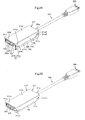
Fig. 2A is a schematic perspective view of the circuit board module with its resin case removed, andFig. 2B is a schematic perspective view of the circuit board module with its shield member further removed. -
Fig.3A is a schematic front view of the circuit board module with its resin case removed, andFig. 3B is a schematic front view of the circuit board module with its shield member further removed. -
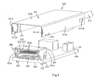
Fig. 4 is an exploded perspective view a circuit board, on which a connector is mounted, and a shield cover of the circuit board module. -
Fig. 5 is a schematic front view of a modified circuit board module, on a circuit board of which a second electronic component is mounted. -
Fig. 6 is a schematic side view of another modified circuit board module, on a circuit board of which two types of connectors are mounted. - Hereinafter, a circuit board module according to an embodiment of the present invention will be described with reference to
Figs. 1 to 4 . The circuit board module shown inFigs. 1 to 4 is a relay device for inputting and outputting digital signals at a high transmission frequency in the range of several tens of MHz to several GHz). The circuit board module is proof against electromagnetic interference (EMI). This circuit board module includes acircuit board 100, a female connector 200 (first electronic component), ashield case 300, acable 400, amale connector 500 and aresin case 600. These respective components will be described in detail below. - The
circuit board 100 is a well-known printed circuit board having afirst surface 101 and asecond surface 102, as shown inFigs. 2A to 4 . On thefirst surface 101 of thecircuit board 100 is mounted thefemale connector 200. Although not shown, thefirst surface 101 is further provided with a plurality of input/output terminals, conductive lines to transmit digital signals, and an IC and other electronic devices. Thesecond surface 102 of thecircuit board 100 is the back side of thefirst surface 101. The conductive lines connect between the input/output terminals andcontacts female connector 200. - The
cable 400 is a well-known cable (e.g. bulk cable) having a plurality of lead wires to transmit the above-described digital signals, as shown inFigs. 1 ,2A and 2B . At an lengthwise end of thecable 400, their lead wires are striped to take out their core wires. The core wires are connected to the input/output terminals by soldering. The other lengthwise end of thecable 400 is connected to themale connector 500. The above-described digital signals are inputted to themale connector 500. - The
female connector 200 is designed to output digital signals. As shown inFigs. 3A, 3B and4 , thefemale connector 200 has abody 210, the plurality of first andsecond contacts metal shell 230. Thebody 210, injection molded in insulating resin, has abase 211 and a projectedportion 212. The projectedportion 212 of a plate shape projects from the front of thebase 211. The first andsecond contacts first contacts 220a are arranged such that their distal end portions are arrayed at intervals along an upper surface of the projectedportion 212, that their intermediate portions are buried in thebase 211, and that their proximal end portions are projected from thebase 211. Thesecond contacts 220b are arranged such that their distal end portions are arrayed at intervals along a lower surface of the projectedportion 212, their intermediate portions are buried in thebase 211, and their proximal end portions are projected from thebase 211. Thefirst contacts 220a and thesecond contacts 220b, are disposed with their phases shifted as shown inFig. 5 . In other words, the distal end portions of thefirst contacts 220a and thesecond contacts 220b are arranged in a zigzag manner when seen from the front.Figs. 3A, 3B ,4 and5 show only the distal end portions of the first andsecond contacts - The
metal shell 230 is fabricated by press-forming a conductive metal plate. As shown inFigs. 3A, 3B and4 , themetal shell 230 has a rectangulartuboid shell body 231 and pairs of first andsecond locking pieces shell body 231. Theshell body 231 fittingly receives thebase 211 of thebody 210 from a rear-side opening of theshell body 231. In this fitted state, the projectedportion 212 of thebody 210 is located inside theshell body 231. Thesecond locking pieces 233 are bent inward at their proximal end portions such that the distal end portions are located inwardly with respect to thefirst locking pieces 232. The first andsecond locking pieces circuit board 100 in the thickness direction. The proximal end portions of the first andsecond contacts first surface 101 of thecircuit board 100 and connected to ends of the conductive lines. Thefemale connector 200 is thus mounted on thefirst surface 101 of thecircuit board 100. Theshell body 231 has a frontside opening that serves as a connection port to fit over a mating male connector (not shown). When the mating male connector is fitted into theshell body 231, theshell body 231 comes into contact with a metal shell of the male connector to establish ground connection.Lateral surfaces 231a at opposite ends of theshell body 231 are recited as "lateral surfaces of a metal shell" in the claims. - The
shield case 300, as shown inFigs. 2A to 4 , has ashield cover 310 for covering thefirst surface 101 of thecircuit board 100 and ashield member 320 for covering thesecond surface 102 of thecircuit board 100. Theshield cover 310 is fabricated by press-forming a conductive metal plate. Theshield cover 310 has acover body 311 of a generally U shape in cross-sectional view, a pair ofcontact portions 312, a sealingplate 313, and a pair of sealingpieces 314. Thecover body 311 has a pair of plate-like side walls 311a and a plate-liketop plate 311b bridging between upper ends (first ends) of theside walls 311a. The distance between outer surfaces of theside walls 311a is substantially the same as a width dimension of thecircuit board 100. Moreover, each length dimension of theside walls 311a and thetop plate 311b is larger than a length dimension of thecircuit board 100. Furthermore, a height dimension of theside walls 311a is slightly larger than a height dimension of thefemale connector 200. That is, theside walls 311a and thetop plate 311b (forming thecover body 311 in combination) cover thefirst surface 101 of thecircuit board 100 and thefemale connector 200. Thetop plate 311b is disposed close to themetal shell 230 of thefemale connector 200 with a slight clearance therebetween. - Moreover, the rear surface of the
top plate 311b is provided continuously with the sealingplate 313, which is a plate body bent downward. The sealingplate 313 covers the rear side of thecover body 311. The sealingplate 313a is provided with a semi-cylindrical lead-outportion 313a. The lead-outportion 313a, together with a semi-cylindrical lead-out portion of theshield member 320, constitutes a cylindrical lead path to lead thecable 400 out theshield case 300. The lead path contacts and connects with an external conductor covering the lead wires at the end of thecable 400. Moreover, the sealingpieces 314 are provided continuously on rear ends of theside walls 311a. The sealingpieces 314 are plate bodies bent inward to abut an outer surface of the sealingplate 313.Fig. 4 shows a state before the sealingpieces 314 are bent. - Moreover, the pair of plate-
like contact portions 312 is continuously provided at front end portions of lower ends (second ends) of theside walls 311a of thecover body 311. Thecontact portions 312 are folded back toward thetop plate 311b. Distal end portions of thecontact portions 312 are bent inward into generally V shapes. The distance between the apexes of the distal end portions is smaller than a width dimension of theshell body 231 of the metal shell 230 (i.e., a distance between thelateral surfaces 231a of the shell body 231). Accordingly, when themetal shell 230 is inserted between the distal end portions of thecontact portions 312, the apexes of the distal end portions of thecontact portions 312 come into elastic contact with thelateral surfaces 231a of theshell body 231 of themetal shell 230 and sandwich them. That is, thecontact portions 312 are plate springs to elastically contact with thelateral surfaces 231a of theshell body 231 of themetal shell 230. Moreover, theside walls 311a have a pair of first locking holes 311a1 in their front end portions and a pair of second locking holes 311a2 in their rear end portions. - The
shield member 320, fabricated by press-forming a conductive metal plate, has amain body 321 of a generally U shape in cross-sectional view, afront plate 322, and a back plate (not shown). Themain body 321 has a pair of plate-like side walls 321a, and a plate-like bottom plate 321b bridging between lower ends of theside walls 321a. A distance between outer surfaces of theside walls 321a is substantially the same as the distance between the outer surfaces of theside walls 311a of theshield cover 310. Moreover, each length dimension of theside walls 321a and thebottom plate 321b is substantially the same as each length dimension of theside walls 311a and thetop plate 311b. Theside walls 321a have rectangular cutouts 321a1 as shown inFig. 2A . Each depth dimension of the cutouts 321a1 is the same as a thickness dimension of thecircuit board 100, and each length dimension of the cutouts 321a1 is slightly larger than the length dimension of thecircuit board 100. The cutouts 321a1 fittingly receives widthwise ends of thecircuit board 100, so that themain body 321 covers thesecond surface 102 of thecircuit board 100. - The
front plate 322 is a plate body extends continuously from the front end of thebottom plate 321b and bent upward. A height dimension of thefront plate 322 is substantially the same as a distance from thetop plate 311b of theshield cover 310 to thebottom plate 321b of theshield member 320. A central portion of an upper end portion of thefront plate 322 is cut out. Thiscutout portion 322a conforms to the shape of the connection port of theconnector 200. That is, thefront plate 322 covers the front side of themain body 321, a front surface of thecircuit board 100, and a portion of theconnector 200 excluding the connection port. The connection port is allowed to be exposed through thecutout portion 322a. The back plate is a plate body extending continuously from the rear end of thebottom plate 321b and bent upward. The back plate covers the rear side of themain body 321 and a rear surface of thecircuit board 100. As mentioned above, the back plate is provided with the a semi-cylindrical lead-out portion. - Widthwise ends of the
front plate 322 are provided with a pair offirst locking projections 322b projecting outward. Rear ends of theside walls 321a are provided with a pair of second locking projections 321a2 projecting outward. The first andsecond locking projections 322b, 321a2 are locked in the first and second locking holes 311a1, 311a2 of theside walls 311a of theshield cover 310. With these projections thus locked in the holes, theshield cover 310 and theshield member 320 are held together sandwiching thecircuit board 100 therebetween. In other words, theshield cover 310 and theshield member 320 are locked to each other, in a state where theshield cover 310 covers thefirst surface 101 of thecircuit board 100 and theshield member 320 covers thesecond surface 102 of thecircuit board 100. The first andsecond locking projections 322b, 321a2 and the first and second locking holes 311a1, 311a2 are recited as "locking means" in the claims. - The
resin case 600 has upper andlower cases Fig. 1 . The upper andlower cases shield case 300 when combined with each other. A front surface of theupper case 610 has anopening 611 to expose the connection port of theconnector 200. A back surface of theupper case 610 has a lead-out hole (not shown) to lead out thecable 400. - The circuit board module having the above-described configuration is assembled in the following steps. First, the
connector 200 is mounted on thefirst surface 101 of thecircuit board 100, and the core wires of thecable 400 are connected by soldering to the respective input/output terminals on thefirst surface 101. The widthwise ends of thecircuit board 100 are then placed into the cutouts 321a1 of theshield member 320. This allows themain body 321 of theshield member 320 to cover thesecond surface 102 of thecircuit board 100, thefront plate 322 of theshield member 320 to cover the front surface of thecircuit board 100 and the surrounding area of the connection port of theconnector 200, and the back plate of theshield member 320 to cover the rear surface of thecircuit board 100. At the same time, thecable 400 is inserted into the lead-out portion of the back plate. - Thereafter, the
shield cover 310 is placed over thecircuit board 100, and the first and second locking holes 311a1, 311a2 of theside walls 311a of theshield cover 310 receive the first andsecond locking projections 322b, 321a2 of theshield member 320. As a result, theshield cover 310 is locked to theshield member 320 in the state where theshield cover 310 covers thefirst surface 101 of thecircuit board 100 and theshield member 320 covers thesecond surface 102 of thecircuit board 100. The combinedshield cover 310 andshield member 320 form theshield case 300 that surrounds thewhole circuit board 100. It should be noted that themetal shell 230 of theconnector 200 mounted on thefirst surface 101 of thecircuit board 100 is inserted between the pair ofcontact portions 312 of theshield cover 310, so that thelateral surfaces 231a of themetal shell 230 urge thecontact portions 312 outward into elastic deformation (that is, thecontact portions 312 are brought into elastic contact with thelateral surfaces 231a of the metal shell 230). Also, the lead-outportion 313a of the sealingplate 313 of theshield cover 310 is combined with the lead-out portion of theshield member 320 so as to cover a portion of thecable 400. Thereafter, the lead-outportion 313a of theshield cover 310 and the lead-out portion of theshield member 320 are caulked and brought into contact and electrical connection with the external conductor of thecable 400. Thereafter, the sealingpieces 314 are bent inward into abutment with the outer surface of the sealingplate 313. - Thereafter, the
shield case 300 is placed inside thelower case 620. Thelower case 620 is then combined with theupper case 610. The combined upper and lower cases, i.e. theresin case 600, thus accommodate thecircuit board 100, theconnector 200, and theshield case 300. At this time, the connection port of themetal shell 230 of theconnector 200 is exposed through theopening 611 of theupper case 610, and thecable 400 is led out through the lead hole of theresin case 600. - The circuit board module as described above has many advantageous features over the conventional art. First, it is possible to connect the
metal shell 230 of thefemale connector 200, theshield cover 310 and theshield member 320 at a time, simply by placing theshield cover 310 over thecircuit board 100, locking the first andsecond locking projections 322b, 321a2 of theshield member 320 into the first and second locking holes 311a1, 311a2 of theside walls 311a of theshield cover 310, and bringing the pair ofcontact portions 312 of theshield cover 310 into elastic contact with thelateral surfaces 231a of themetal shell 230 of thefemale connector 200 mounted on thecircuit board 100. This configuration remarkably simplifies the connection work of thecontact portions 312 with themetal shell 230, leading to reduced assembly cost of the circuit board module. Second, thecontact portions 312 are adapted to elastically contact with thelateral surfaces 231a of themetal shell 230 to sandwich themetal shell 230, so that electric connection between thecontact portions 312 and themetal shell 230 is improved in stability and reliability. Third, as thecontact portions 312 make elastic contact with thelateral surfaces 231a of themetal shell 230, thetop plate 311b of theshield cover 310 can be disposed close to thefemale connector 200, contributing to reduction in height dimension of the circuit board module. - The circuit board module is also advantageous because of the minimized number of components. More particularly, the
shield cover 310 and theshield member 320 are adapted to be locked to each other, with thecircuit board 100 sandwiched therebetween, simply by locking the first andsecond locking projections 322b, 321a2 of theshield member 320 into the first and second locking holes 311a1, 311a2 of theside walls 311a of theshield cover 310. It is thus possible to omit additional locking means for locking theshield cover 310 and theshield member 320 to thecircuit board 100, reducing the number of components and resulting in reduced cost of the circuit board module. Further, as thecircuit board 100 has no locking holes or the like for locking theshield cover 310 and theshield member 320 to thecircuit board 100, it should obviate the need to reserve the space for forming the locking holes or the like in thecircuit board 100. Consequently, thecircuit board 100 can be downsized, and the circuit board module can be accordingly downsized. - Lastly, the
contact portions 312, being plate springs that are extended from the lower ends of theside walls 311a of thecover body 311 of theshield cover 310 and folded back toward thetop plate 311b, has another advantageous feature over the conventional art. Particularly, compared to a conventional case where the contact portions are formed by cutting out and raising portions of the cover body such that cutout portions are formed in the cover body, the circuit board module having the above describedcontact portions 312 is less likely to leak electromagnetic waves occurring from thefemale connector 200 and other components from theshield cover 310. - The above-described circuit board module is not limited to the above embodiment but may be modified in design as desired within the range of the claims. Modification examples will be described in detail below.
- The
shield case 300 of the above embodiment has theshield cover 310 and theshield member 320, but the present invention is not limited thereto. The invention only requires a shield cover that covers thefirst surface 101 of thecircuit board 100 if the electronic components, such as thefemale connector 200 and an IC, and the conductive lines are provided only on thefirst surface 101 of thecircuit board 100. The above-describedshield cover 310 is shaped to cover thefirst surface 101 of thecircuit board 100, but the shield cover may be modified in shape as needed, as long as it has such a shape as to cover at least the first electronic component such as thefemale connector 200 on thefirst surface 101 of thecircuit board 100. Moreover, theshield member 320 has such a shape as to cover thesecond surface 102 of thecircuit board 100, but the present invention is not limited thereto. For example, in a case as shown inFig. 5 where a secondelectronic component 700 is mounted on thesecond surface 102 of thecircuit board 100, the shield member may have such a shape as to cover at least the second electronic component. - Moreover, the
shield cover 310 and theshield member 320 of the above embodiment are each formed by press-forming a conductive metal plate, but the present invention is not limited thereto. For example, the shield cover and/or the shield member may be fabricated based on a housing made of insulating resin or ceramics, on inner surfaces of which a conductive thin film may be formed or conductive metal may be deposited. Alternatively, the shield cover and/or the shield member may be cast in conductive metal. - The locking means for locking the
shield cover 310 to theshield member 320 may or may not be the first and second locking holes 311a1, 311a2 and the first andsecond locking projections 322b, 321a2 used in the above embodiment. For example, the first andsecond locking projections 322b, 321a2 may be provided on theside walls 311a of theshield cover 310, and the first and second locking holes 311a1, 311a2 may be provided in theside walls 321a of theshield member 320. Alternatively, theside walls 311a and theside walls 321a may be formed with locking holes communicating to each other to receive pins or screws therethrough. Moreover, theshield cover 310 and theshield member 320 may be locked to thecircuit board 100 as themetal shell 230 is. - The
shield cover 310 has the pair ofcontact portions 312 in the above embodiment, but it only needs to have at least onecontact portion 312. Moreover, thecontact portion 312 is not limited to a plate spring extended from the lower end of aside wall 311a of thecover body 311 and folded back, but the contact portion may be modified in design as needed as long as it is elastically contactable from a side with alateral surface 231a of themetal shell 230. For example, the contact portion may be a circular arc-shaped metal plate, a coil spring, a body made of conductive elastic resin or the like, and it may be attached to an inner side surface of aside wall 311a of thecover body 311. The contact portion in any one of the above configurations may be brought into elastic contact with the metal shell, which forms an outer shell of the first electronic component, but it may be brought into elastic contact with a ground/earth terminal provided on a lateral surface of the first electronic component. In the latter case, the first electronic component may be a transistor or other electronic components. - The
female connector 200 in the above embodiment is adapted to output digital signals, the female connector 200 (first electronic component) may be a female or male connector adapted to input or input/output signals. Moreover, in the circuit board module of the above embodiment, only thefemale connector 200 is mounted on thefirst surface 101 of thecircuit board 100, but the invention is not limited thereto and two or more types of first electronic components may be mounted. For example,Fig. 6 illustrates a modified module, wherein a female connector 200' is mounted on a front end portion of thefirst surface 101 of thecircuit board 100, and amale connector 200" is mounted on a rear end portion of thefirst surface 101. In this modified module as well, a shield cover 310' covers thefirst surface 101 of thecircuit board 100, and first andsecond contact portions 312a', 312b' of the shield cover 310' are brought into elastic contact with lateral surfaces of a metal shell 230' of the female connector 200' and ametal shell 230" of themale connector 200", respectively. Obviously, the first andsecond contact portions 312a', 312b' may also be provided in pairs to sandwich the lateral surfaces of the metal shell 230' of the female connector 200' and the lateral surfaces of themetal shell 230" of themale connector 200" , respectively. It is also possible to provide a plurality of first electronic components of the same type to be mounted on thefirst surface 101 of thecircuit board 100. If a plurality of or a plurality of types of first electronic components are mounted on thecircuit board 100, cables 400 (led out from the respective first electronic components) may be connected to thecircuit board 100. Moreover, the core wires of thecable 400 may be connected to the input/output terminals of thecircuit board 100, but they may be connected directly to the first electronic component such as thefemale connector 200. - The
cable 400 and themale connector 500 may be omitted as in the case shown inFig. 6 . Moreover, theresin case 600 may also be omitted, especially in the case where the first electronic component, such as the connector of the present circuit board module, is used as an interface for electronic equipment or the like. - Materials, shapes, numbers, dimensions and the like constructing the respective portions of the circuit board module in the above embodiment have been described only as examples, and they may be modified as desired as long as they can realize similar functions. Moreover, the present invention is not limited to the relay device as in the above embodiment, but the invention can be applied to various circuit board modules, such as the above-described interface for electronic equipment.
-
- 100
- circuit board
101 first surface
102 second surface - 200
- female connector (first electronic component)
210 body
220a first contact
220b second contact
230 metal shell
231a lateral surface - 300
- shield case
310 shield cover
311 cover body
311a side wall portion
311a1 first locking hole (locking means)
311a2 second locking hole (locking means)
311b top plate
312 contact portion
320 shield member
321a2 second locking projected portion (locking means)
322b first locking projected portion (locking means) - 400
- cable
- 500
- male connector
- 600
- resin case
Claims (13)
- A shield cover (310) adapted to cover at least a first electronic component (200) mounted on a first surface (101) of a circuit board (100), the first electronic component having a metal shell (230) or having a ground/earth terminal on a lateral surface (231a) thereof, the shield cover comprising:a contact portion (312) being elastically contactable with a lateral surface (231a) of the metal shell (230) or the ground/earth terminal of the first electronic component.
- The shield cover according to claim 1, which includes a pair of contact portions (312),
wherein the contact portions are elastically contactable with opposite lateral surfaces (231a) of the metal shell or with the ground/earth terminal from opposite sides of the first electronic component (200). - The shield cover according to claim 1 or 2, further comprising a cover body (311) of a generally U shape in cross-sectional view, wherein
the cover body includes a pair of side walls (311a), each of which has first and second ends, and a top plate (311b) bridging between the first ends of the side walls,
the contact portion comprises a plate spring extended from the second end of one of the side walls of the cover body and folded back toward the top plate of the cover body. - The shield cover according to any one of claims 1 to 3, having a shape adapted to cover the first surface (101) of the circuit board (100).
- A shield case comprising:the shield cover according to any one of claims 1 to 4; anda shield member (320) adapted to cover a second surface (102) of the circuit board, the second surface being an opposite surface to the first surface (101) of the circuit board.
- A shield case comprising:the shield cover according to any one of claims 1 to 4; anda shield member (320) adapted to cover at least a second electronic component mounted on a second surface (102) of the circuit board, the second surface being an opposite surface to the first surface (101) of the circuit board.
- The shield case according to claim 5 or claim 6, further comprising locking means (311a1, 311a2) for locking the shield cover to the shield member with the circuit board sandwiched therebetween.
- A circuit board module comprising:the shield cover according to any one of claims 1 to 4, or the shield case according to claim 5;a first electronic component (200) having the metal shell or having the ground/earth terminal on the lateral surface thereof; anda circuit board (100) having the first surface (101) on which the first electronic component is mounted.
- A circuit board module comprising:the shield case according to claim 6;a first electronic component (200) having the metal shell (230) or having the ground/earth terminal on the lateral surface thereof;a second electronic component; anda circuit board (100) having the first surface (101) on which the first electronic component is mounted and the second surface (102) on which the second electronic component is mounted, the second surface being an opposite surface to the first surface of the circuit board.
- The circuit board module according to claim 8 or claim 9, wherein the first electronic component (200) is a female or male connector.
- The circuit board module according to claim 10, further comprising a cable (400), the cable being connected to the first electronic component or connected to the first electronic component via a conductive line on the circuit board.
- The circuit board module according to claim 8 or 9, wherein
the first electronic component comprises at least two first electronic components that are mounted on the first surface (101) of the circuit board, and
one of the first electronic components is a female connector, and the other first electronic component is a male connector. - The circuit board module according to any one of claims 8 to 12, further comprising a case (600) made of insulating resin and adapted to cover the shield case.
Applications Claiming Priority (1)
| Application Number | Priority Date | Filing Date | Title |
|---|---|---|---|
| JP2009235899A JP5525227B2 (en) | 2009-10-13 | 2009-10-13 | Board module |
Publications (2)
| Publication Number | Publication Date |
|---|---|
| EP2312701A1 true EP2312701A1 (en) | 2011-04-20 |
| EP2312701B1 EP2312701B1 (en) | 2016-02-17 |
Family
ID=43446394
Family Applications (1)
| Application Number | Title | Priority Date | Filing Date |
|---|---|---|---|
| EP10251553.3A Not-in-force EP2312701B1 (en) | 2009-10-13 | 2010-09-03 | Printed circuit board module |
Country Status (6)
| Country | Link |
|---|---|
| US (1) | US8503191B2 (en) |
| EP (1) | EP2312701B1 (en) |
| JP (1) | JP5525227B2 (en) |
| KR (1) | KR101811874B1 (en) |
| CN (1) | CN102044802B (en) |
| TW (1) | TWI513125B (en) |
Families Citing this family (18)
| Publication number | Priority date | Publication date | Assignee | Title |
|---|---|---|---|---|
| CN103042560A (en) * | 2011-10-13 | 2013-04-17 | 亚旭电子科技(江苏)有限公司 | Substrate module transfer method and magnetic board applying to same |
| CN103124484B (en) * | 2011-11-21 | 2017-01-25 | 富泰华工业(深圳)有限公司 | Electronic device |
| US20150264840A1 (en) * | 2013-01-10 | 2015-09-17 | Mitsubishi Electric Corporation | Electronic device |
| DE102013101731A1 (en) | 2013-02-21 | 2014-09-04 | Epcos Ag | Pressure Sensor System |
| DE102013101732A1 (en) * | 2013-02-21 | 2014-08-21 | Epcos Ag | sensor system |
| CN204243363U (en) | 2014-02-21 | 2015-04-01 | 番禺得意精密电子工业有限公司 | electrical connector |
| CN107146981B (en) * | 2014-05-26 | 2019-03-22 | 富士康(昆山)电脑接插件有限公司 | Socket connector |
| WO2015196913A1 (en) * | 2014-06-27 | 2015-12-30 | 深圳市得润电子股份有限公司 | Cable connector assembly, plate-end connector assembly, and electric connector combination thereof |
| CN204216285U (en) | 2014-07-15 | 2015-03-18 | 番禺得意精密电子工业有限公司 | Electric connector |
| CN109149279B (en) * | 2017-06-16 | 2024-07-16 | 泰科电子(上海)有限公司 | Connector components |
| CN107567274B (en) * | 2017-11-03 | 2020-03-31 | 成都芯通科技股份有限公司 | PCB signal unit shielding grounding device |
| CN108490384B (en) * | 2018-03-30 | 2024-08-02 | 深圳海岸语音技术有限公司 | Small-sized space sound source azimuth detection device and method thereof |
| USD888675S1 (en) * | 2018-08-29 | 2020-06-30 | Samsung Electronics Co., Ltd. | Case for a circuit board |
| USD888676S1 (en) * | 2018-08-29 | 2020-06-30 | Samsung Electronics Co., Ltd. | Case for a circuit board |
| CN111211452B (en) * | 2018-11-21 | 2021-07-13 | 启碁科技股份有限公司 | electronic device |
| JP2021086985A (en) * | 2019-11-29 | 2021-06-03 | 日立Astemo株式会社 | Electronic control device |
| JP2022049268A (en) * | 2020-09-16 | 2022-03-29 | セイコーエプソン株式会社 | Electronic apparatus and spectroscopic camera |
| US12010825B2 (en) | 2022-03-15 | 2024-06-11 | Snap Inc. | Eyewear with RF shielding having grounding springs |
Citations (7)
| Publication number | Priority date | Publication date | Assignee | Title |
|---|---|---|---|---|
| EP0998178A1 (en) * | 1998-10-30 | 2000-05-03 | Framatome Connectors International | Device for fixing a jack connector on a mobile phone circuit board |
| US20020142656A1 (en) * | 2001-03-28 | 2002-10-03 | Chih-Kai Chang | Connector and metal grounding shell arrangement |
| US20020191384A1 (en) * | 2001-06-19 | 2002-12-19 | Shin-Fu Wei | Metal housing grounding mechanism |
| US20080070439A1 (en) * | 2006-09-20 | 2008-03-20 | Fujitsu Limited | Connector mounting structure |
| US20080166918A1 (en) * | 2007-01-08 | 2008-07-10 | Speed Tech Corp. | Three-in-one connector set |
| JP2009123500A (en) | 2007-11-14 | 2009-06-04 | Hosiden Corp | Base board assembly |
| US7547217B1 (en) * | 2008-09-12 | 2009-06-16 | U.D. Electronic Corp. | Structure of electrical connector |
Family Cites Families (20)
| Publication number | Priority date | Publication date | Assignee | Title |
|---|---|---|---|---|
| JPH07112639B2 (en) | 1989-06-28 | 1995-12-06 | 義一 久世 | Die set type automatic press machine manufacturing method |
| JPH0332498U (en) * | 1989-08-08 | 1991-03-29 | ||
| JPH0668347U (en) * | 1993-02-26 | 1994-09-22 | ミツミ電機株式会社 | Electrical signal filter |
| JPH0727194U (en) * | 1993-10-04 | 1995-05-19 | 東京コスモス電機株式会社 | Printed circuit board shielding structure |
| JP3331421B2 (en) * | 1994-07-11 | 2002-10-07 | マスプロ電工株式会社 | Electronic device case |
| US5603620A (en) * | 1995-08-04 | 1997-02-18 | Delco Electronics Corp. | Integrated printed circuit connector and ground clip assembly |
| US6089882A (en) * | 1996-11-27 | 2000-07-18 | The Whitaker Corporation | Memory card connector with grounding clip |
| US6139365A (en) * | 1998-11-10 | 2000-10-31 | Hon Hai Precision Ind. Co., Ltd. | Centronic connector assembly |
| TW435873U (en) * | 1998-12-08 | 2001-05-16 | Hon Hai Prec Ind Co Ltd | Cable connector assembly |
| US6095862A (en) * | 1999-02-04 | 2000-08-01 | Molex Incorporated | Adapter frame assembly for electrical connectors |
| US6276965B1 (en) * | 1999-05-25 | 2001-08-21 | 3Com Corporation | Shielded I/O connector for compact communications device |
| JP2002271080A (en) * | 2001-03-09 | 2002-09-20 | Toshiba Corp | High frequency device |
| CN2483851Y (en) * | 2001-05-04 | 2002-03-27 | 莫列斯公司 | Electric connector |
| US7113410B2 (en) * | 2004-04-01 | 2006-09-26 | Lucent Technologies, Inc. | Electromagnetic shield assembly with opposed hook flanges |
| JP2008027975A (en) * | 2006-07-18 | 2008-02-07 | Teac Corp | Noise shielding mechanism |
| US7581967B2 (en) * | 2006-08-16 | 2009-09-01 | Sandisk Corporation | Connector with ESD protection |
| US7572145B1 (en) * | 2008-06-27 | 2009-08-11 | Hon Hai Precision Ind. Co., Ltd. | Cable assembly having reinforcement structure protecting interior shielding structure |
| CN201323333Y (en) * | 2008-12-11 | 2009-10-07 | 富士康(昆山)电脑接插件有限公司 | Cable connector component |
| CN101752723B (en) * | 2008-12-11 | 2012-11-28 | 富士康(昆山)电脑接插件有限公司 | Electric coupler |
| JP4436436B2 (en) * | 2009-07-14 | 2010-03-24 | カネソウ株式会社 | Water-flow covering device for grooves |
-
2009
- 2009-10-13 JP JP2009235899A patent/JP5525227B2/en not_active Expired - Fee Related
-
2010
- 2010-06-25 TW TW099120824A patent/TWI513125B/en not_active IP Right Cessation
- 2010-08-03 KR KR1020100074967A patent/KR101811874B1/en not_active Expired - Fee Related
- 2010-08-23 US US12/861,186 patent/US8503191B2/en not_active Expired - Fee Related
- 2010-09-03 EP EP10251553.3A patent/EP2312701B1/en not_active Not-in-force
- 2010-10-12 CN CN201010506577.1A patent/CN102044802B/en not_active Expired - Fee Related
Patent Citations (7)
| Publication number | Priority date | Publication date | Assignee | Title |
|---|---|---|---|---|
| EP0998178A1 (en) * | 1998-10-30 | 2000-05-03 | Framatome Connectors International | Device for fixing a jack connector on a mobile phone circuit board |
| US20020142656A1 (en) * | 2001-03-28 | 2002-10-03 | Chih-Kai Chang | Connector and metal grounding shell arrangement |
| US20020191384A1 (en) * | 2001-06-19 | 2002-12-19 | Shin-Fu Wei | Metal housing grounding mechanism |
| US20080070439A1 (en) * | 2006-09-20 | 2008-03-20 | Fujitsu Limited | Connector mounting structure |
| US20080166918A1 (en) * | 2007-01-08 | 2008-07-10 | Speed Tech Corp. | Three-in-one connector set |
| JP2009123500A (en) | 2007-11-14 | 2009-06-04 | Hosiden Corp | Base board assembly |
| US7547217B1 (en) * | 2008-09-12 | 2009-06-16 | U.D. Electronic Corp. | Structure of electrical connector |
Also Published As
| Publication number | Publication date |
|---|---|
| KR20110041980A (en) | 2011-04-22 |
| TWI513125B (en) | 2015-12-11 |
| US8503191B2 (en) | 2013-08-06 |
| TW201125237A (en) | 2011-07-16 |
| JP5525227B2 (en) | 2014-06-18 |
| CN102044802B (en) | 2016-03-02 |
| EP2312701B1 (en) | 2016-02-17 |
| US20110085317A1 (en) | 2011-04-14 |
| KR101811874B1 (en) | 2017-12-22 |
| JP2011086644A (en) | 2011-04-28 |
| CN102044802A (en) | 2011-05-04 |
Similar Documents
| Publication | Publication Date | Title |
|---|---|---|
| EP2312701B1 (en) | Printed circuit board module | |
| KR101413531B1 (en) | Electric connector | |
| KR101471283B1 (en) | Electrical connector for use with a circuit board | |
| US9559469B2 (en) | Connector | |
| CN109845047B (en) | connector structure | |
| USRE44448E1 (en) | Electrical connector with ESD protection | |
| JP2539197Y2 (en) | Shielded electrical connector assembly | |
| US9343835B2 (en) | Terminal and connector having the same | |
| US7651372B2 (en) | Electric connector with shields on mating housings | |
| US10819071B2 (en) | Connector structure that is reconfigurable to accommodate either an STP cable or a UTP cable | |
| US5516294A (en) | Coaxial interconnection system | |
| EP3411928B1 (en) | Plug connector with integrated galvanic separation and shielding element | |
| US10403995B2 (en) | Electrical connector, electronic component, and assembly method | |
| US6623301B2 (en) | Plug connector for electronic devices | |
| US12500363B2 (en) | Electrical connector, manufacturing method, and connector assembly with improved reliability | |
| US9385487B2 (en) | Active plug connector and method for assembling the same | |
| US9231352B2 (en) | Module, and connection structure of module and mating connector | |
| CN113169471B (en) | Electrical connector assembly and installation structure of the electrical connector assembly | |
| US11791593B2 (en) | Connector-equipped multicore cable | |
| US12237638B2 (en) | Connector | |
| JP2026040913A (en) | connector | |
| CN120569858A (en) | Connector with a plurality of connectors |
Legal Events
| Date | Code | Title | Description |
|---|---|---|---|
| PUAI | Public reference made under article 153(3) epc to a published international application that has entered the european phase |
Free format text: ORIGINAL CODE: 0009012 |
|
| AK | Designated contracting states |
Kind code of ref document: A1 Designated state(s): AL AT BE BG CH CY CZ DE DK EE ES FI FR GB GR HR HU IE IS IT LI LT LU LV MC MK MT NL NO PL PT RO SE SI SK SM TR |
|
| AX | Request for extension of the european patent |
Extension state: BA ME RS |
|
| 17P | Request for examination filed |
Effective date: 20111007 |
|
| 17Q | First examination report despatched |
Effective date: 20120910 |
|
| GRAP | Despatch of communication of intention to grant a patent |
Free format text: ORIGINAL CODE: EPIDOSNIGR1 |
|
| INTG | Intention to grant announced |
Effective date: 20151001 |
|
| GRAS | Grant fee paid |
Free format text: ORIGINAL CODE: EPIDOSNIGR3 |
|
| GRAA | (expected) grant |
Free format text: ORIGINAL CODE: 0009210 |
|
| AK | Designated contracting states |
Kind code of ref document: B1 Designated state(s): AL AT BE BG CH CY CZ DE DK EE ES FI FR GB GR HR HU IE IS IT LI LT LU LV MC MK MT NL NO PL PT RO SE SI SK SM TR |
|
| REG | Reference to a national code |
Ref country code: GB Ref legal event code: FG4D |
|
| REG | Reference to a national code |
Ref country code: CH Ref legal event code: EP |
|
| REG | Reference to a national code |
Ref country code: IE Ref legal event code: FG4D |
|
| REG | Reference to a national code |
Ref country code: AT Ref legal event code: REF Ref document number: 776017 Country of ref document: AT Kind code of ref document: T Effective date: 20160315 |
|
| REG | Reference to a national code |
Ref country code: DE Ref legal event code: R096 Ref document number: 602010030659 Country of ref document: DE |
|
| REG | Reference to a national code |
Ref country code: NL Ref legal event code: MP Effective date: 20160217 |
|
| REG | Reference to a national code |
Ref country code: LT Ref legal event code: MG4D |
|
| REG | Reference to a national code |
Ref country code: AT Ref legal event code: MK05 Ref document number: 776017 Country of ref document: AT Kind code of ref document: T Effective date: 20160217 |
|
| PG25 | Lapsed in a contracting state [announced via postgrant information from national office to epo] |
Ref country code: ES Free format text: LAPSE BECAUSE OF FAILURE TO SUBMIT A TRANSLATION OF THE DESCRIPTION OR TO PAY THE FEE WITHIN THE PRESCRIBED TIME-LIMIT Effective date: 20160217 Ref country code: NO Free format text: LAPSE BECAUSE OF FAILURE TO SUBMIT A TRANSLATION OF THE DESCRIPTION OR TO PAY THE FEE WITHIN THE PRESCRIBED TIME-LIMIT Effective date: 20160517 Ref country code: FI Free format text: LAPSE BECAUSE OF FAILURE TO SUBMIT A TRANSLATION OF THE DESCRIPTION OR TO PAY THE FEE WITHIN THE PRESCRIBED TIME-LIMIT Effective date: 20160217 Ref country code: GR Free format text: LAPSE BECAUSE OF FAILURE TO SUBMIT A TRANSLATION OF THE DESCRIPTION OR TO PAY THE FEE WITHIN THE PRESCRIBED TIME-LIMIT Effective date: 20160518 Ref country code: IT Free format text: LAPSE BECAUSE OF FAILURE TO SUBMIT A TRANSLATION OF THE DESCRIPTION OR TO PAY THE FEE WITHIN THE PRESCRIBED TIME-LIMIT Effective date: 20160217 |
|
| REG | Reference to a national code |
Ref country code: FR Ref legal event code: PLFP Year of fee payment: 7 |
|
| PG25 | Lapsed in a contracting state [announced via postgrant information from national office to epo] |
Ref country code: LT Free format text: LAPSE BECAUSE OF FAILURE TO SUBMIT A TRANSLATION OF THE DESCRIPTION OR TO PAY THE FEE WITHIN THE PRESCRIBED TIME-LIMIT Effective date: 20160217 Ref country code: AT Free format text: LAPSE BECAUSE OF FAILURE TO SUBMIT A TRANSLATION OF THE DESCRIPTION OR TO PAY THE FEE WITHIN THE PRESCRIBED TIME-LIMIT Effective date: 20160217 Ref country code: LV Free format text: LAPSE BECAUSE OF FAILURE TO SUBMIT A TRANSLATION OF THE DESCRIPTION OR TO PAY THE FEE WITHIN THE PRESCRIBED TIME-LIMIT Effective date: 20160217 Ref country code: SE Free format text: LAPSE BECAUSE OF FAILURE TO SUBMIT A TRANSLATION OF THE DESCRIPTION OR TO PAY THE FEE WITHIN THE PRESCRIBED TIME-LIMIT Effective date: 20160217 Ref country code: NL Free format text: LAPSE BECAUSE OF FAILURE TO SUBMIT A TRANSLATION OF THE DESCRIPTION OR TO PAY THE FEE WITHIN THE PRESCRIBED TIME-LIMIT Effective date: 20160217 Ref country code: PL Free format text: LAPSE BECAUSE OF FAILURE TO SUBMIT A TRANSLATION OF THE DESCRIPTION OR TO PAY THE FEE WITHIN THE PRESCRIBED TIME-LIMIT Effective date: 20160217 Ref country code: PT Free format text: LAPSE BECAUSE OF FAILURE TO SUBMIT A TRANSLATION OF THE DESCRIPTION OR TO PAY THE FEE WITHIN THE PRESCRIBED TIME-LIMIT Effective date: 20160617 |
|
| PG25 | Lapsed in a contracting state [announced via postgrant information from national office to epo] |
Ref country code: EE Free format text: LAPSE BECAUSE OF FAILURE TO SUBMIT A TRANSLATION OF THE DESCRIPTION OR TO PAY THE FEE WITHIN THE PRESCRIBED TIME-LIMIT Effective date: 20160217 Ref country code: DK Free format text: LAPSE BECAUSE OF FAILURE TO SUBMIT A TRANSLATION OF THE DESCRIPTION OR TO PAY THE FEE WITHIN THE PRESCRIBED TIME-LIMIT Effective date: 20160217 |
|
| PGFP | Annual fee paid to national office [announced via postgrant information from national office to epo] |
Ref country code: GB Payment date: 20160831 Year of fee payment: 7 Ref country code: DE Payment date: 20160831 Year of fee payment: 7 |
|
| REG | Reference to a national code |
Ref country code: DE Ref legal event code: R097 Ref document number: 602010030659 Country of ref document: DE |
|
| PG25 | Lapsed in a contracting state [announced via postgrant information from national office to epo] |
Ref country code: RO Free format text: LAPSE BECAUSE OF FAILURE TO SUBMIT A TRANSLATION OF THE DESCRIPTION OR TO PAY THE FEE WITHIN THE PRESCRIBED TIME-LIMIT Effective date: 20160217 Ref country code: CZ Free format text: LAPSE BECAUSE OF FAILURE TO SUBMIT A TRANSLATION OF THE DESCRIPTION OR TO PAY THE FEE WITHIN THE PRESCRIBED TIME-LIMIT Effective date: 20160217 Ref country code: SM Free format text: LAPSE BECAUSE OF FAILURE TO SUBMIT A TRANSLATION OF THE DESCRIPTION OR TO PAY THE FEE WITHIN THE PRESCRIBED TIME-LIMIT Effective date: 20160217 Ref country code: SK Free format text: LAPSE BECAUSE OF FAILURE TO SUBMIT A TRANSLATION OF THE DESCRIPTION OR TO PAY THE FEE WITHIN THE PRESCRIBED TIME-LIMIT Effective date: 20160217 |
|
| PGFP | Annual fee paid to national office [announced via postgrant information from national office to epo] |
Ref country code: FR Payment date: 20160816 Year of fee payment: 7 |
|
| PLBE | No opposition filed within time limit |
Free format text: ORIGINAL CODE: 0009261 |
|
| STAA | Information on the status of an ep patent application or granted ep patent |
Free format text: STATUS: NO OPPOSITION FILED WITHIN TIME LIMIT |
|
| PG25 | Lapsed in a contracting state [announced via postgrant information from national office to epo] |
Ref country code: BE Free format text: LAPSE BECAUSE OF FAILURE TO SUBMIT A TRANSLATION OF THE DESCRIPTION OR TO PAY THE FEE WITHIN THE PRESCRIBED TIME-LIMIT Effective date: 20160217 |
|
| 26N | No opposition filed |
Effective date: 20161118 |
|
| PG25 | Lapsed in a contracting state [announced via postgrant information from national office to epo] |
Ref country code: BG Free format text: LAPSE BECAUSE OF FAILURE TO SUBMIT A TRANSLATION OF THE DESCRIPTION OR TO PAY THE FEE WITHIN THE PRESCRIBED TIME-LIMIT Effective date: 20160517 Ref country code: SI Free format text: LAPSE BECAUSE OF FAILURE TO SUBMIT A TRANSLATION OF THE DESCRIPTION OR TO PAY THE FEE WITHIN THE PRESCRIBED TIME-LIMIT Effective date: 20160217 |
|
| PG25 | Lapsed in a contracting state [announced via postgrant information from national office to epo] |
Ref country code: MC Free format text: LAPSE BECAUSE OF FAILURE TO SUBMIT A TRANSLATION OF THE DESCRIPTION OR TO PAY THE FEE WITHIN THE PRESCRIBED TIME-LIMIT Effective date: 20160217 |
|
| REG | Reference to a national code |
Ref country code: CH Ref legal event code: PL |
|
| REG | Reference to a national code |
Ref country code: IE Ref legal event code: MM4A |
|
| PG25 | Lapsed in a contracting state [announced via postgrant information from national office to epo] |
Ref country code: LI Free format text: LAPSE BECAUSE OF NON-PAYMENT OF DUE FEES Effective date: 20160930 Ref country code: CH Free format text: LAPSE BECAUSE OF NON-PAYMENT OF DUE FEES Effective date: 20160930 Ref country code: IE Free format text: LAPSE BECAUSE OF NON-PAYMENT OF DUE FEES Effective date: 20160903 |
|
| PG25 | Lapsed in a contracting state [announced via postgrant information from national office to epo] |
Ref country code: LU Free format text: LAPSE BECAUSE OF NON-PAYMENT OF DUE FEES Effective date: 20160903 |
|
| REG | Reference to a national code |
Ref country code: DE Ref legal event code: R119 Ref document number: 602010030659 Country of ref document: DE |
|
| GBPC | Gb: european patent ceased through non-payment of renewal fee |
Effective date: 20170903 |
|
| PG25 | Lapsed in a contracting state [announced via postgrant information from national office to epo] |
Ref country code: HU Free format text: LAPSE BECAUSE OF FAILURE TO SUBMIT A TRANSLATION OF THE DESCRIPTION OR TO PAY THE FEE WITHIN THE PRESCRIBED TIME-LIMIT; INVALID AB INITIO Effective date: 20100903 Ref country code: CY Free format text: LAPSE BECAUSE OF FAILURE TO SUBMIT A TRANSLATION OF THE DESCRIPTION OR TO PAY THE FEE WITHIN THE PRESCRIBED TIME-LIMIT Effective date: 20160217 |
|
| PG25 | Lapsed in a contracting state [announced via postgrant information from national office to epo] |
Ref country code: TR Free format text: LAPSE BECAUSE OF FAILURE TO SUBMIT A TRANSLATION OF THE DESCRIPTION OR TO PAY THE FEE WITHIN THE PRESCRIBED TIME-LIMIT Effective date: 20160217 Ref country code: MT Free format text: LAPSE BECAUSE OF NON-PAYMENT OF DUE FEES Effective date: 20160930 Ref country code: MK Free format text: LAPSE BECAUSE OF FAILURE TO SUBMIT A TRANSLATION OF THE DESCRIPTION OR TO PAY THE FEE WITHIN THE PRESCRIBED TIME-LIMIT Effective date: 20160217 Ref country code: HR Free format text: LAPSE BECAUSE OF FAILURE TO SUBMIT A TRANSLATION OF THE DESCRIPTION OR TO PAY THE FEE WITHIN THE PRESCRIBED TIME-LIMIT Effective date: 20160217 Ref country code: IS Free format text: LAPSE BECAUSE OF FAILURE TO SUBMIT A TRANSLATION OF THE DESCRIPTION OR TO PAY THE FEE WITHIN THE PRESCRIBED TIME-LIMIT Effective date: 20160217 |
|
| REG | Reference to a national code |
Ref country code: FR Ref legal event code: ST Effective date: 20180531 |
|
| PG25 | Lapsed in a contracting state [announced via postgrant information from national office to epo] |
Ref country code: DE Free format text: LAPSE BECAUSE OF NON-PAYMENT OF DUE FEES Effective date: 20180404 Ref country code: GB Free format text: LAPSE BECAUSE OF NON-PAYMENT OF DUE FEES Effective date: 20170903 |
|
| PG25 | Lapsed in a contracting state [announced via postgrant information from national office to epo] |
Ref country code: FR Free format text: LAPSE BECAUSE OF NON-PAYMENT OF DUE FEES Effective date: 20171002 |
|
| PG25 | Lapsed in a contracting state [announced via postgrant information from national office to epo] |
Ref country code: AL Free format text: LAPSE BECAUSE OF FAILURE TO SUBMIT A TRANSLATION OF THE DESCRIPTION OR TO PAY THE FEE WITHIN THE PRESCRIBED TIME-LIMIT Effective date: 20160217 |