EP2312688A2 - Wireless communication device and method of using the same - Google Patents
Wireless communication device and method of using the same Download PDFInfo
- Publication number
- EP2312688A2 EP2312688A2 EP20100173856 EP10173856A EP2312688A2 EP 2312688 A2 EP2312688 A2 EP 2312688A2 EP 20100173856 EP20100173856 EP 20100173856 EP 10173856 A EP10173856 A EP 10173856A EP 2312688 A2 EP2312688 A2 EP 2312688A2
- Authority
- EP
- European Patent Office
- Prior art keywords
- antenna element
- top panel
- antenna
- panel
- connector
- Prior art date
- Legal status (The legal status is an assumption and is not a legal conclusion. Google has not performed a legal analysis and makes no representation as to the accuracy of the status listed.)
- Withdrawn
Links
Images


Classifications
-
- H—ELECTRICITY
- H01—ELECTRIC ELEMENTS
- H01Q—ANTENNAS, i.e. RADIO AERIALS
- H01Q1/00—Details of, or arrangements associated with, antennas
- H01Q1/12—Supports; Mounting means
- H01Q1/22—Supports; Mounting means by structural association with other equipment or articles
- H01Q1/24—Supports; Mounting means by structural association with other equipment or articles with receiving set
- H01Q1/241—Supports; Mounting means by structural association with other equipment or articles with receiving set used in mobile communications, e.g. GSM
- H01Q1/242—Supports; Mounting means by structural association with other equipment or articles with receiving set used in mobile communications, e.g. GSM specially adapted for hand-held use
- H01Q1/243—Supports; Mounting means by structural association with other equipment or articles with receiving set used in mobile communications, e.g. GSM specially adapted for hand-held use with built-in antennas
Definitions
- the present invention relates to a wireless communication device having an antenna element accommodating a wide frequency band with a high gain while satisfying the needs for a smaller size and a smaller thickness.
- the IEEE 802.16e standard i.e., the WiMAX communication
- WiMAX communication has been increasingly used as a standard for performing the Internet communication in a mobile device such as a computer.
- the WiMAX communication is performed while a wireless communication device (dongle) having an IC substrate, an antenna, and the like, provided therein is connected to a mobile device.
- Patent Document 1 An example of such a wireless communication device is the one described in Patent Document 1.
- the dongle described in Patent Document 1 is directed to a dongle used for the access of a guest device to a wireless home network, and includes a memory and a processing unit that are connected to the guest device using an antenna and a configuration free interface. The access of the guest device is realized via this dongle.
- a dipole antenna is a type of an antenna for performing a wireless communication in the above-described wireless communication device (dongle).
- an antenna element needs to be formed with a total width of 1/2 wavelength with each element having a 1/4 wavelength width according to the communication frequency. Therefore, it can be said that this is an antenna requiring a relatively large area.
- an antenna element 28 is provided at an end of a dongle body 27 as shown in FIG. 12 , thus reducing the effective area thereof.
- an antenna structure with a small effective area can be used for making a product dedicated to a particular frequency.
- the shape of the antenna element needs to be improved, thereby arising a need for some extra area.
- the present invention is made in view of the problems described above, and it is therefore an object of the present invention to provide a wireless communication device having an antenna element accommodating a wide frequency band with a high gain while satisfying the needs for a smaller size and a smaller thickness.
- a first aspect of the present invention is directed to a wireless communication device, including a housing and a substrate having a connector for connecting with a mobile device and a communication electronic component provided inside the housing, wherein an antenna element constituted by an antenna element ground portion and an antenna element portion is formed in a sheet shape generally across an entire surface of a top panel of the housing.
- a second aspect of the present invention is directed to a wireless communication device, including a housing of a rectangular parallelepiped shape constituted by a lower case and an upper case including a top panel and side panels extending vertically from a circumference of the top panel and a substrate having a connector for connecting with a mobile device and a communication electronic component provided inside the housing, wherein an antenna element constituted by an antenna element ground portion and an antenna element portion is formed in a sheet shape generally across an entire surface of the top panel of the upper case.
- a third aspect of the present invention is directed to an embodiment of the wireless communication device, wherein the antenna element is formed in a sheet shape generally across an entire outer surface of the top panel.
- a fourth aspect of the present invention is directed to an embodiment of the wireless communication device, wherein the antenna element is formed in a sheet shape generally across an entire inner surface of the top panel.
- a fifth aspect of the present invention is directed to an embodiment of the wireless communication device, wherein the antenna element is disposed on a flexible printed circuit, and the flexible printed circuit is provided on the outer surface or the inner surface of the top panel.
- a sixth aspect of the present invention is directed to an embodiment of the wireless communication device, wherein the flexible printed circuit is further extended across the side panel and bonded thereto, so that the antenna element is formed extending from the top panel to an outer surface or an inner surface of the side panel.
- a seventh aspect of the present invention is directed to an embodiment of the wireless communication device, wherein the antenna element portion is disposed on one side of the flexible printed circuit formed by a predetermined dielectric material, and the antenna element ground portion is disposed on the other side of the flexible printed circuit.
- An eighth aspect of the present invention is directed to an embodiment of the wireless communication device, wherein the antenna element is integrally molded with the top panel, and the antenna element is disposed on each of an inner side and an outer side of the top panel at different positions in a thickness direction of the top panel.
- a ninth aspect of the present invention is directed to an embodiment of the wireless communication device, wherein the antenna element is formed by punching and bending a conductive metal, and at least a portion of the antenna element that is furthest away by planar distance among the antenna element portion and the antenna element ground portion is disposed on the outer side of the top panel.
- a tenth aspect of the present invention is directed to an embodiment of the wireless communication device, wherein the antenna element and the top panel are integrally molded while a predetermined dielectric material is fixed to one of the antenna element ground portion and the antenna element portion and the dielectric material is closely in contact with the other of the antenna element ground portion and the antenna element portion.
- An eleventh aspect of the present invention is directed an embodiment of the wireless communication device, wherein a dielectric layer is disposed so as to be in contact with an upper surface of one of the antenna element ground portion and the antenna element portion and a lower surface of the other of the antenna element ground portion and the antenna element portion, whereby the dielectric layer is provided between the antenna element ground portion and the antenna element portion.
- a twelfth aspect of the present invention is directed to an embodiment of the wireless communication device, wherein the antenna element is formed by subjecting the top panel of the upper case to a plating process.
- a thirteenth aspect of the present invention is directed to an embodiment of the wireless communication device, wherein a portion of the antenna element formed by the plating process is extended from the top panel to the side panel.
- a fourteenth aspect of the present invention is directed to an embodiment of the wireless communication device, wherein a protruding portion is provided in the top panel by outwardly deforming a portion of the outer surface of the top panel, and at least a portion of the antenna element that is furthest away from among the antenna element portion and the antenna element ground portion is provided in the protruding portion.
- a fifteenth aspect of the present invention is directed to an embodiment of the wireless communication device, wherein a depressed portion is provided by depressing a portion of the inner surface of the top panel, and at least a portion of the antenna element that is furthest away from among the antenna element portion and the antenna element ground portion is provided in the depressed portion.
- a sixteenth aspect of the present invention is directed to an embodiment of the wireless communication device, wherein the antenna element ground portion and the antenna element portion partially overlap with each other in a planar view.
- a seventeenth aspect of the present invention is directed to an embodiment of the wireless communication device, wherein the antenna element is connected to an antenna electrode provided in the substrate via a capacitive coupling element.
- An eighteenth aspect of the present invention is directed to an embodiment of the wireless communication device, wherein the antenna element is connected to an antenna electrode provided in the substrate via an electrical connector.
- a nineteenth aspect of the present invention is directed to an embodiment of the wireless communication device, wherein: the housing is of a rectangular parallelepiped shape and has a quadrangular top panel and a quadrangular bottom panel parallel to each other and four side panels vertically extending from a circumference of the top panel; the antenna element is provided on the top panel; the connector is provided on one of the side panels; and the antenna element is positioned horizontally when the bottom panel is placed at a bottom surface, and the antenna element is positioned vertically when another one of the side panels perpendicular to the side panel at which the connector is provided is placed at a bottom surface, with the connector being fitted into a counterpart connector connected to a mobile device via a cable.
- a twentieth aspect of the present invention is directed to a method of using a wireless communication device including: a housing of a rectangular parallelepiped shape having a quadrangular top panel and a quadrangular bottom panel parallel to each other and four side panels vertically extending from a circumference of the top panel; a substrate having a connector for connecting with a mobile device and a communication electronic component provided inside the housing so that the connector is provided on one of the four side panels; and an antenna element constituted by an antenna element ground portion and an antenna element portion being formed in a sheet shape generally across the top panel, wherein the wireless communication device is used in an upright position such that one of the side panels perpendicular to the side panel at which the connector is provided is placed as a bottom surface with the connector being fitted into a counterpart connector connected to a mobile device via a cable.
- the antenna element is formed in a sheet shape generally across the entire surface of the top panel of the housing, thus providing a wireless communication device with an antenna element having a large effective area and accommodating a wide frequency band with a high gain while satisfying the needs for a smaller size and a smaller thickness.
- the antenna element is provided on the flexible printed circuit, and the flexible printed circuit is provided on the outer surface or the inner surface of the top panel.
- the flexible printed circuit with the antenna element formed thereon can be bonded while being curved, thereby increasing the degree of freedom in design.
- the flexible printed circuit is further extended across the side panel and bonded thereto, so that the antenna element is formed extending from the top panel to an outer surface or an inner surface of the side panel.
- the side panel is also utilized as the antenna effective area, thereby facilitating a further reduction in size as a whole.
- the antenna element portion is disposed on one side of the flexible printed circuit formed by a predetermined dielectric material, and the antenna element ground portion is disposed on the other side of the flexible printed circuit.
- the antenna element is integrally molded with the top panel, and the antenna element is disposed on each of an inner side and an outer side of the top panel at different positions in a thickness direction of the top panel.
- the antenna element portion (not the antenna element ground portion) on the outer side of the top panel, for example, the antenna element portion can be further away from the substrate.
- the integral molding increases the degree of freedom in the layout.
- the antenna element is formed by punching and bending a conductive metal, and at least a portion of the antenna element portion that is furthest away by planar distance among the antenna element portion and the antenna element ground portion is disposed on the outer side of the top panel.
- a portion of the antenna element can be disposed further away from the substrate, thereby increasing the antenna effect.
- the antenna element and the top panel are integrally molded while a predetermined dielectric material is fixed to one of the antenna element ground portion and the antenna element portion and the dielectric material is closely in contact with the other of the antenna element ground portion and the antenna element portion.
- a dielectric layer is disposed so as to be in contact with an upper surface of one of the antenna element ground portion and the antenna element portion and a lower surface of the other of the antenna element ground portion and the antenna element portion, whereby the dielectric layer is provided between the antenna clement ground portion and the antenna element portion.
- the antenna element since the antenna element is formed by subjecting the top panel of the upper case to a plating process, the antenna element can be formed directly on the upper case constituting the housing.
- a portion of the antenna element formed by the plating process is extended from the top panel to the side panel.
- the side panel can be also utilized as the effective area of the antenna, thereby allowing for a further reduction in size as a whole.
- a protruding portion is provided on the top panel by outwardly deforming a portion of the outer surface of the top panel, and at least a portion of the antenna element that is furthest away from among the antenna element portion and the antenna element ground portion is provided in the protruding portion.
- a portion of the antenna element can be disposed further away from the substrate, thereby increasing the antenna effect.
- a depressed portion is provided by depressing a portion of the inner surface of the top panel, and at least a portion of the antenna element that is furthest away from among the antenna element portion and the antenna element ground portion is provided in the depressed portion.
- a portion of the antenna element can be disposed further away from the substrate, thereby increasing the antenna effect.
- the antenna element ground portion and the antenna element portion partially overlap with each other in a planar view, thereby increasing the capacity of the antenna and thus achieving a wider bandwidth.
- the antenna element is connected to an antenna electrode provided in the substrate via a capacitive coupling element, thereby ensuring the antenna performance.
- the antenna element is connected to an antenna electrode provided in the substrate via an electrical connector, the process of soldering, or the like, is omitted, thereby simplifying the assembling step.
- the wireless communication device can be used in an upright position such that one of the side panels perpendicular to the side panel at which the connector is provided is placed as a bottom surface with the antenna element being positioned high and vertically.
- the method of using a wireless communication device that further improves the antenna sensitivity can be implemented.
- a wireless communication device of the present invention includes: a housing of a rectangular parallelepiped shape that is constituted by a lower case and an upper case having an elongated top panel and side panels circumferentially-provided around the top panel; and a substrate having a connector for connecting with a mobile device and a communication electronic component provided inside the housing.
- a pair of dipole antennas is formed in a sheet shape generally across an entire surface of the top panel of the upper case.
- MIMO Multiple Input Multiple Output
- the wireless communication device When used, the wireless communication device is placed on a flat surface with a top panel of the lower case 12 facing downward and the top panel of the upper case 11 being placed horizontally and facing upward, while a USB cable connected to, for example, a USB terminal of a mobile device is connected to the connector of the wireless communication device.
- Embodiments to be described below are different from each other in terms of the process of forming an antenna element 18 on a top panel 14 of the upper case 11 constituting the housing.
- Embodiment 1 will be described in detail. In the following embodiments, however, only the points different from those of the other embodiments in a method for forming the antenna element 18 will be described.
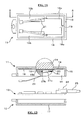
- FIGS. 1A and 1B show a wireless communication device 10 according to Embodiment 1 of the present invention.
- FIG. 1A is a plan view showing an upper case 11 constituting a housing as viewed from an inner side thereof
- FIG. 1B is a cross-sectional view of the upper case 11, a lower case 12, and a substrate 13 unassembled, as viewed from the side surface.
- the external dimensions of the wireless communication device 10 are 23 mm in length, 46.5 mm in width (see FIG. 1A ) and 13.5 mm in height (the height after the upper case 11 and the lower case 12 of FIG. 1B are assembled together).
- the thickness of a top panel 14 is 1 mm.
- the wireless communication device 10 of the present invention includes a housing constituted by the hollow upper case 11 and the hollow lower case 12 attached to each other at portions of short side panels 15 and long side panel 16.
- Each of the upper case 11 and the lower case 12 is of a generally rectangular parallelepiped shape, and the top panel 14 and a bottom panel 17 have the largest areas.
- the substrate 13 having thereon a connector 22 for connecting with a mobile device and an electronic component such as an IC which enables wireless communications such as WiMAX communication is provided on an inner side of the lower case 12 so that the connector 22 is exposed at the short side panel 15.
- An antenna element 18 is formed in a sheet shape on an inner surface of the top panel 14 of the upper case 11.
- the upper case 11 and the lower case 12 are formed by molding a resin, and the antenna element 18 is made of a conductive metal, for example.
- the "antenna element 18" used herein refers to both an antenna element portion 18a and an antenna element ground portion 18b.
- the antenna element portion 18a and the antenna element ground portion 18b are first formed on a flexible printed circuit (hereinafter referred to as an "FPC") 19 in a sheet form, and the thus-obtained structure is then bonded to the inner surface of the top panel 14 by means of an adhesive 20, as shown in FIG. 1B .
- FPC flexible printed circuit
- An antenna cable 21 is connected to the bonded antenna element 18 such that a center conductor 21 a of the antenna cable is soldered to the antenna element portion 18a and a net portion 21 b of the antenna cable is soldered to the antenna element ground portion 18b. Thereafter, a connector of the antenna cable 21 is connected to the connector of the substrate 13, and the upper case 11, the lower case 12 and the substrate 13 are assembled to obtain the wireless communication device 10.
- the wireless communication device 10 is used, for example, by connecting with a mobile device via a USB cable 23 with the USB cable 23 being connected to the connector 22.
- the antenna element 18 may include two symmetrically-arranged, L-shaped antenna element portions 18a and two symmetrically-arranged, generally I-shaped antenna element ground portions 18b as shown in FIG. 1A .
- a dipole antenna is formed by the antenna element portions 18a and antenna element ground portions 18b in such an arrangement.
- the antenna element portions 18a and antenna element ground portions 18b are respectively arranged close to the four corners of a rectangle which is a face of the top panel 14 of a generally rectangular parallelepiped shape shown in FIG. 1A so that the two pairs of antennas are widely disposed generally across the entire surface of the top panel 14.
- the antenna element 18 on the top panel 14 that has the largest area and is away from the substrate 13, it becomes possible to accommodate a wide frequency band with a high gain and to achieve further reductions in size and thickness.
- the present invention is not limited thereto.
- a technique in which a sheet of the FPC 19 with the antenna element 18 formed thereon is bonded to the inner side of the top panel 14 of the upper case 11, even when the upper case 11 has the top panel 14 of a curved shape, for example, the sheet of the FPC 19 with the antenna element 18 thereon can be bonded while being curved.
- the degree of freedom in design is increased.
- the antenna performance can be further improved by forming a protruding portion 29 that protrudes outwardly from a portion of the top panel 14 and disposing the short side portion of the L-shape of the antenna element portion 18a on an inner side of the protruding portion 29, so that the antenna element portion 18a can be further away from the substrate 13 by the height of the protrusion as shown in FIG. 7A .
- the effective portion to be provided in the protruding portion 29 is a portion furthest away from a portion connected to the antenna cable 21 (substrate connecting portion).
- the short side portion of the L-shape of the antenna element portion 18a is provided in the protruding portion 29.
- the present invention is not limited to the case where the protruding portion 29 is provided as in FIG. 7A .
- the antenna performance can be further improved by reducing the thickness of a portion of the top panel 14 within a range of the thickness thereof to form a depressed portion and by disposing the short side portion of the L-shape of the antenna element portion 18a in the depressed portion so that the portion of the antenna element portion 18a can be further away from the substrate 13 by the height of the depression.
- means to provide the antenna element 18 on the top panel 14 is not limited to the method in which the FPC 19 with the antenna element 18 thereon is bonded to the top panel 14.
- the antenna element 18 may be arranged on the top panel 14 in the similar manner to that of FIGS. 7A to 7C by using a plating process, integral molding, or the like, to be described later.
- the resonance frequency is decreased with the FPC 19, and the unfolded antenna length is shortened, thereby exhibiting the shortening effect.
- the antenna element portion 18a and the antenna element ground portion 18b which are arranged on different surfaces may be partially overlapped with each other as shown in FIG. 9A , thereby increasing the capacity thereof and thus achieving a wider bandwidth.
- Embodiment 2 is basically the same as Embodiment 1, like elements to those of Embodiment 1 will be denoted by like reference numerals and the description thereof will be omitted.
- a through hole 24 is formed running through the upper case 11 and the FPC 19, and the cable 21 is passed therethrough and soldered to the antenna element 18, for example, as shown in FIG. 2B .
- the antenna effect is increased by forming the antenna element 18 on the outer side of the top panel 14 of the upper case 11 as in Embodiment 2 so that the antenna element 18 can be away from the substrate.
- the antenna performance can be further improved by forming the protruding portion 29 that protrudes outwardly from a portion of the top panel 14 and disposing the short side portion of the L-shape of the antenna element portion 18a on the outer side of the protruding portion 29 so that the short side portion can be further away from the substrate 13 by the height of the protrusion.
- the effective portion to be provided in the protruding portion 29 is a portion furthest away from a portion connected to the antenna cable 21 (substrate connecting portion).
- the short side portion of the L-shape of the antenna element portion 18a is provided at the protruding portion 29.
- through holes 35 may be formed as shown in FIG. 7C , and the antenna element 18 may be connected to the antenna cable 21 at the inner side of the top panel 14 via the through holes 35.
- Embodiment 3 is basically the same as Embodiment 1, like elements to those of Embodiment 1 will be denoted by like reference numerals and the description thereof will be omitted.
- a portion thereof denoted by a solid line is disposed on the outer side of the upper case 11, and a portion thereof denoted by a broken line is disposed on the inner side of the upper case 11.
- the inner side portion of the antenna element 18 is connected to the outer side portion of the antenna element 18 (see FIG. 3B ).
- the upper case 11 shown in FIGS. 3A and 3B can be fabricated, for example, by forming such a bent antenna element 18 by molding in advance, and then burying the obtained antenna element 18 in the upper case 11 in the process of molding the upper case 11. Note that when it is difficult to complete the integral molding process in a single step, the primary molding process may be performed to give a partially-finished product which is finished in the following secondary molding process.
- the wireless communication device 10 is fabricated by forming the upper case 11 as shown in FIGS. 3A and 3B , connecting the connector of the antenna cable 21 that is connected to the antenna element 18 with the connector of the substrate 13, and then assembling the upper case 11, the lower case 12 and the substrate 13. As a result, the portion of the antenna element portion 18a that is formed on the outer side of the upper case 11 can be further away from the substrate 13 by an amount equal to the thickness of the top panel 14, thus increasing the antenna effect.
- the antenna element portion 18a can be further away from the substrate by an amount equal to the thickness of the top panel 14 as described above, the distance between the substrate 13 and the top panel 14 may be shortened.
- the antenna element portion 18a and the antenna element ground portion 18b can be directly connected to electrodes 31 of the substrate 13 via capacitive coupling (C coupling) elements 30.
- C coupling capacitive coupling
- Examples of the case using the capacitive coupling element 30 include a case where a chip condenser is used and a case where the connection is made via a dielectric material.
- the arrangement of the antenna element 18 same as that of FIGS. 3A and 3B can be obtained using the FPC 19.
- the antenna element can be similarly arranged by burying, in the upper case 11, the FPC 19 on which the antenna element 18 of a predetermined shape has been printed and which has been subjected to the bending process.
- the antenna element portion 18a and the antenna element ground portion 18b may be directly connected to the electrodes 31 of the substrate 13 via an electrical connector 32 as shown in FIG. 8B .
- the electrical connector 32 includes, for example, contact portions 33 for contacting the antenna element portion 18a and the antenna element ground portion 18b, and substrate connecting portions 34 electrically connected to the contact portions 33 as shown in FIG. 8C .
- connection as shown in FIG. 8A or 8B eliminates the need for using a coaxial cable, reduces the thickness of the upper case 11, and ensures the antenna performance.
- the antenna element portion 18a may be disposed on the outer side of the top panel 14 and pass through the inner surface of the top panel 14 by providing a through hole whose inner wall is plated. Then, the antenna element portion 18a is connected to the electrode 31 of the substrate 13 on the inner surface of the top panel 14 using the capacitive coupling element 30 or the electrical connector 32. Then, the connection can be made without a cable, the antenna performance can be ensured, and the fabrication can be performed easily and inexpensively.
- the antenna element portion 18a disposed on the outer side of the top panel 14 may partially overlap in a planar view with the antenna element ground portion 18b disposed on the inner side of the top panel 14. As a result, the distance between the antenna element portion 18a and the antenna element ground portion 18b in the thickness direction of the top panel 14 is reduced, and the capacitance is thus increased. Therefore, it is possible to achieve the wider bandwidth.
- the antenna element portion 18a may be connected in advance with the antenna element ground portion 18b using a coaxial cable, soldering and the like, and then integral molding can be performed as shown in FIGS. 9A and 9B .
- the antenna element ground portion 18b is provided with a hole slightly lager than the outer dimensions of the net portion 21b of the antenna cable 21, the antenna cable 21 is passed through the hole, the center conductor 21 a is soldered to the lower surface of the antenna element portion 18a, and the net portion 21b having passed through the hole is soldered to the antenna element ground portion 18b. Integral molding with the upper case 11 in such an arrangement as shown in FIG. 9B can be then performed.
- a double mold process wherein a dielectric material having a predetermined dielectric constant is molded between the antenna element portion 18a and the antenna element ground portion 18b in the primary molding process and the upper case 11 is completed in the secondary molding process by burying, in the upper case 11, the antenna element portion 18a and the antenna element ground portion 18b with the dielectric material therebetween, the resonance frequency is decreased and the unfolded antenna length is shortened, thereby exhibiting the shortening effect.
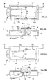
- FIGS. 4A and 4B show a wireless communication device 10 according to Embodiment 4 of the present invention.
- FIG. 4A is a bottom view showing the upper case 11 constituting a housing as viewed from an inner side thereof
- FIG. 4B is a cross-sectional view of the upper case 11 unassembled, as viewed from the side of the long side panel 16.
- the dielectric layer 25 is provided between the antenna elements 18.
- the dielectric layer 25 is formed between the antenna element portion 18a and the antenna element ground portion 18b by first forming the antenna element portion 18a on the inner side of the upper case 11 using a plating process, for example, then forming the dielectric layer 25 thereon across the entire inner surface of the upper case 11, and forming the antenna clement ground portion 18b on the dielectric layer 25 using a plating process, for example.
- the plating process can be performed by suitably using masking or a laser
- the Laser-Direct-Structuring (LSD) technique is favorable in that a plating process can be easily performed even on protruding or depressed surfaces with a laser.
- the antenna element portion 18a or the antenna element ground portion 18b can be disposed on the protruding portion or depressed portion of the upper case 11, thereby making it possible to dispose the antenna element portion 18a further away from the above-described substrate.
- the wireless communication device 10 is fabricated by forming the upper case 11 as shown in FIGS. 4A and 4B , connecting the connector of the antenna cable 21 that is connected to the antenna element 18 with the connector of the substrate 13, and then assembling the upper case 11, the lower case 12 and the substrate 13. Note that the dielectric layer 25 is provided with a solder hole 26 for soldering.
- the wavelength shortening effect of the dielectric material reduces the effective area necessary for the antenna element 18, and a further reduction in size as a whole can be thus achieved.
- FIGS. 5A and 5B show a wireless communication device 10 according to Embodiment 5 of the present invention.
- FIG. 5A is a bottom view showing the upper case 11 constituting a housing as viewed from an inner side thereof
- FIG. 5B is a cross-sectional view of the upper case 11 unassembled, as viewed from the side of the short side panel 15.
- the antenna element 18 is extended and bent so as to reach the side of the long side panel 16.
- the antenna element portion 18a and the antenna element ground portion 18b are extended and bent to reach the side of the long side panel 16 so that antenna element bent portions 18c and 18d are respectively formed.
- Examples of the specific processing method include a plating process with masking.
- the antenna element 18 is extended only to reach the side of the long side panel 16 in the example shown in FIGS. 5A and 5B , it is also possible to extend the antenna element 18 to reach the side of the short side panel 15.
- the side panel can be also utilized as the effective area of the antenna, thereby allowing for a further reduction in size as a whole.
- the antenna element portion 18a and the antenna element ground portion 18b are respectively extended and bent to reach the side of the long side panel 16 so that antenna element bent portions 18c and 18d are formed.
- the antenna element bent portions 18c and 18d may be formed.
- the method for forming the antenna element 18 may be such that a conductive metal plate that has been subjected to a pressing process so as to achieve the arrangement as described above on the upper case 11 is integrally molded with the upper case 11 or such that the FPC 19 with the antenna element formed thereon that has been subjected to a bending process may be integrally molded with the upper case 11.
- the antenna element portion 18a is provided on the outer surface of the top panel 14, the antenna element portion 18a is allowed to be drawn to the inner surface of the top panel 14 by means using the cable 21 shown in FIGS. 2A and 2B , or means using the through holes 35 shown in FIG. 7C .
- the present invention is not limited thereto.
- a capacitive coupling element 37 may be provided inside the top panel 14, and the antenna element portion 18a that is provided on the outer surface of the top panel 14 may be virtually drawn to the inner surface of the top panel 14 via the capacitive coupling element 37.
- the capacitive coupling element 37 in this case may be buried in the top panel 14 or may be fitted into a hole made through the top panel 14.
- the connector 22 is provided at the short side panel 15 in Embodiments 1 to 7, the present invention is not limited thereto.
- the connector 22 may be provided at the long side panel 16. If the connector 22 is formed at the side of the long side panel 16 and the wireless communication device 10 is connected to a mobile device 36 via the USB cable 22 having a predetermined length allowing for a bend of ⁇ 90° or more, the use of the wireless communication device 10 is not limited to such a case that the top panel of the upper case 11 with the antenna element provided thereon is placed horizontally and facing the planar surface upwardly while the top panel of the lower case 12 is used as the bottom surface as in Embodiments 1 to 7.
- the wireless communication device 10 can stand lengthwise when used with one of the two short side panels 15 being the bottom surface thereof.
- the antenna element 18 can be made to stand vertically, and one end of the antenna element portion 18a or the antenna element ground portion 18b (a portion of the antenna element between the antenna element portion and the antenna element ground portion that is farthest away from the other) can be positioned high, thereby further improving the antenna sensitivity without using a particular kind of structure such as a conventional flip structure.
- the end of the antenna element portion 18a is preferably positioned higher as shown in FIG. 10 so as to obtain a better antenna sensitivity.
- the present invention has been described using a housing of a rectangular parallelepiped shape in Embodiments 1 to 7 described above, the present invention is not limited thereto.
- the present invention can be applied also in a cylindrical housing with the top panel 14 of a circular shape, for example.
- the present invention is not limited thereto.
- the present invention is effective also in the case where one antenna element portion 18a and one antenna element ground portion 18b are disposed.
Abstract
A wireless communication device (10) having an antenna element (18) accommodating a wide frequency band with a high gain while satisfying the needs for a smaller size and a smaller thickness is provided. The wireless communication device (10) includes: a housing of a rectangular parallelepiped shape that is constituted by a lower case (12) and an upper case (11) having an elongated top panel (14) and side panels (15, 16) circumferentially-provided around the top panel (14); and a substrate (13) having a connector (22) for connecting with a mobile device and a communication electronic component provided inside the housing, wherein an antenna element (18) is formed in a sheet shape generally across an entire surface of the top panel (14) of the upper case (11).
Description
- The present invention relates to a wireless communication device having an antenna element accommodating a wide frequency band with a high gain while satisfying the needs for a smaller size and a smaller thickness.
- In recent years, the IEEE 802.16e standard, i.e., the WiMAX communication, has been increasingly used as a standard for performing the Internet communication in a mobile device such as a computer. The WiMAX communication is performed while a wireless communication device (dongle) having an IC substrate, an antenna, and the like, provided therein is connected to a mobile device.
- An example of such a wireless communication device is the one described in
Patent Document 1. The dongle described inPatent Document 1 is directed to a dongle used for the access of a guest device to a wireless home network, and includes a memory and a processing unit that are connected to the guest device using an antenna and a configuration free interface. The access of the guest device is realized via this dongle. - A dipole antenna is a type of an antenna for performing a wireless communication in the above-described wireless communication device (dongle). In the dipole antenna, an antenna element needs to be formed with a total width of 1/2 wavelength with each element having a 1/4 wavelength width according to the communication frequency. Therefore, it can be said that this is an antenna requiring a relatively large area.
- In a conventional wireless communication device, however, an
antenna element 28 is provided at an end of adongle body 27 as shown inFIG. 12 , thus reducing the effective area thereof. In order to increase the effective area of theantenna element 28 provided at the end of thedongle body 27, it is necessary to increase the size of thedongle body 27, thus failing to satisfy the needs for a smaller size. Such an antenna structure with a small effective area can be used for making a product dedicated to a particular frequency. However, in order to make a product accommodating a wide frequency band, the shape of the antenna element needs to be improved, thereby arising a need for some extra area. - The present invention is made in view of the problems described above, and it is therefore an object of the present invention to provide a wireless communication device having an antenna element accommodating a wide frequency band with a high gain while satisfying the needs for a smaller size and a smaller thickness.
- A first aspect of the present invention is directed to a wireless communication device, including a housing and a substrate having a connector for connecting with a mobile device and a communication electronic component provided inside the housing, wherein an antenna element constituted by an antenna element ground portion and an antenna element portion is formed in a sheet shape generally across an entire surface of a top panel of the housing.
- A second aspect of the present invention is directed to a wireless communication device, including a housing of a rectangular parallelepiped shape constituted by a lower case and an upper case including a top panel and side panels extending vertically from a circumference of the top panel and a substrate having a connector for connecting with a mobile device and a communication electronic component provided inside the housing, wherein an antenna element constituted by an antenna element ground portion and an antenna element portion is formed in a sheet shape generally across an entire surface of the top panel of the upper case.
- A third aspect of the present invention is directed to an embodiment of the wireless communication device, wherein the antenna element is formed in a sheet shape generally across an entire outer surface of the top panel.
- A fourth aspect of the present invention is directed to an embodiment of the wireless communication device, wherein the antenna element is formed in a sheet shape generally across an entire inner surface of the top panel.
- A fifth aspect of the present invention is directed to an embodiment of the wireless communication device, wherein the antenna element is disposed on a flexible printed circuit, and the flexible printed circuit is provided on the outer surface or the inner surface of the top panel.
- A sixth aspect of the present invention is directed to an embodiment of the wireless communication device, wherein the flexible printed circuit is further extended across the side panel and bonded thereto, so that the antenna element is formed extending from the top panel to an outer surface or an inner surface of the side panel.
- A seventh aspect of the present invention is directed to an embodiment of the wireless communication device, wherein the antenna element portion is disposed on one side of the flexible printed circuit formed by a predetermined dielectric material, and the antenna element ground portion is disposed on the other side of the flexible printed circuit.
- An eighth aspect of the present invention is directed to an embodiment of the wireless communication device, wherein the antenna element is integrally molded with the top panel, and the antenna element is disposed on each of an inner side and an outer side of the top panel at different positions in a thickness direction of the top panel.
- A ninth aspect of the present invention is directed to an embodiment of the wireless communication device, wherein the antenna element is formed by punching and bending a conductive metal, and at least a portion of the antenna element that is furthest away by planar distance among the antenna element portion and the antenna element ground portion is disposed on the outer side of the top panel.
- A tenth aspect of the present invention is directed to an embodiment of the wireless communication device, wherein the antenna element and the top panel are integrally molded while a predetermined dielectric material is fixed to one of the antenna element ground portion and the antenna element portion and the dielectric material is closely in contact with the other of the antenna element ground portion and the antenna element portion.
- An eleventh aspect of the present invention is directed an embodiment of the wireless communication device, wherein a dielectric layer is disposed so as to be in contact with an upper surface of one of the antenna element ground portion and the antenna element portion and a lower surface of the other of the antenna element ground portion and the antenna element portion, whereby the dielectric layer is provided between the antenna element ground portion and the antenna element portion.
- A twelfth aspect of the present invention is directed to an embodiment of the wireless communication device, wherein the antenna element is formed by subjecting the top panel of the upper case to a plating process.
- A thirteenth aspect of the present invention is directed to an embodiment of the wireless communication device, wherein a portion of the antenna element formed by the plating process is extended from the top panel to the side panel.
- A fourteenth aspect of the present invention is directed to an embodiment of the wireless communication device, wherein a protruding portion is provided in the top panel by outwardly deforming a portion of the outer surface of the top panel, and at least a portion of the antenna element that is furthest away from among the antenna element portion and the antenna element ground portion is provided in the protruding portion.
- A fifteenth aspect of the present invention is directed to an embodiment of the wireless communication device, wherein a depressed portion is provided by depressing a portion of the inner surface of the top panel, and at least a portion of the antenna element that is furthest away from among the antenna element portion and the antenna element ground portion is provided in the depressed portion.
- A sixteenth aspect of the present invention is directed to an embodiment of the wireless communication device, wherein the antenna element ground portion and the antenna element portion partially overlap with each other in a planar view.
- A seventeenth aspect of the present invention is directed to an embodiment of the wireless communication device, wherein the antenna element is connected to an antenna electrode provided in the substrate via a capacitive coupling element.
- An eighteenth aspect of the present invention is directed to an embodiment of the wireless communication device, wherein the antenna element is connected to an antenna electrode provided in the substrate via an electrical connector.
- A nineteenth aspect of the present invention is directed to an embodiment of the wireless communication device, wherein: the housing is of a rectangular parallelepiped shape and has a quadrangular top panel and a quadrangular bottom panel parallel to each other and four side panels vertically extending from a circumference of the top panel; the antenna element is provided on the top panel; the connector is provided on one of the side panels; and the antenna element is positioned horizontally when the bottom panel is placed at a bottom surface, and the antenna element is positioned vertically when another one of the side panels perpendicular to the side panel at which the connector is provided is placed at a bottom surface, with the connector being fitted into a counterpart connector connected to a mobile device via a cable.
- A twentieth aspect of the present invention is directed to a method of using a wireless communication device including: a housing of a rectangular parallelepiped shape having a quadrangular top panel and a quadrangular bottom panel parallel to each other and four side panels vertically extending from a circumference of the top panel; a substrate having a connector for connecting with a mobile device and a communication electronic component provided inside the housing so that the connector is provided on one of the four side panels; and an antenna element constituted by an antenna element ground portion and an antenna element portion being formed in a sheet shape generally across the top panel, wherein the wireless communication device is used in an upright position such that one of the side panels perpendicular to the side panel at which the connector is provided is placed as a bottom surface with the connector being fitted into a counterpart connector connected to a mobile device via a cable.
- In accordance with any one of the first to fourth aspects, the antenna element is formed in a sheet shape generally across the entire surface of the top panel of the housing, thus providing a wireless communication device with an antenna element having a large effective area and accommodating a wide frequency band with a high gain while satisfying the needs for a smaller size and a smaller thickness.
- In accordance with the fifth aspect, the antenna element is provided on the flexible printed circuit, and the flexible printed circuit is provided on the outer surface or the inner surface of the top panel. Thus, even when the upper case has the top panel of a curved shape, for example, the flexible printed circuit with the antenna element formed thereon can be bonded while being curved, thereby increasing the degree of freedom in design.
- In accordance with the sixth aspect, the flexible printed circuit is further extended across the side panel and bonded thereto, so that the antenna element is formed extending from the top panel to an outer surface or an inner surface of the side panel. Thus, the side panel is also utilized as the antenna effective area, thereby facilitating a further reduction in size as a whole.
- In accordance with the seventh aspect, the antenna element portion is disposed on one side of the flexible printed circuit formed by a predetermined dielectric material, and the antenna element ground portion is disposed on the other side of the flexible printed circuit. With the wavelength shortening effect of the dielectric material, the effective area necessary for the antenna element is reduced, and a further reduction in size as a whole can be thus achieved.
- In accordance with the eighth aspect, the antenna element is integrally molded with the top panel, and the antenna element is disposed on each of an inner side and an outer side of the top panel at different positions in a thickness direction of the top panel. Thus, by forming the antenna element portion (not the antenna element ground portion) on the outer side of the top panel, for example, the antenna element portion can be further away from the substrate. Also, the integral molding increases the degree of freedom in the layout.
- In accordance with the ninth aspect, the antenna element is formed by punching and bending a conductive metal, and at least a portion of the antenna element portion that is furthest away by planar distance among the antenna element portion and the antenna element ground portion is disposed on the outer side of the top panel. Thus, a portion of the antenna element can be disposed further away from the substrate, thereby increasing the antenna effect.
- In accordance with the tenth aspect, the antenna element and the top panel are integrally molded while a predetermined dielectric material is fixed to one of the antenna element ground portion and the antenna element portion and the dielectric material is closely in contact with the other of the antenna element ground portion and the antenna element portion. With the wavelength shortening effect of the dielectric material, the effective area necessary for the antenna element is reduced, and a further reduction in size as a whole can be thus achieved.
- In accordance with the eleventh aspect, a dielectric layer is disposed so as to be in contact with an upper surface of one of the antenna element ground portion and the antenna element portion and a lower surface of the other of the antenna element ground portion and the antenna element portion, whereby the dielectric layer is provided between the antenna clement ground portion and the antenna element portion. With the wavelength shortening effect of the dielectric material, the effective area necessary for the antenna element is reduced, and a further reduction in size as a whole can be thus achieved.
- In accordance with the twelfth aspect, since the antenna element is formed by subjecting the top panel of the upper case to a plating process, the antenna element can be formed directly on the upper case constituting the housing.
- In accordance with the thirteenth aspect, a portion of the antenna element formed by the plating process is extended from the top panel to the side panel. Thus, the side panel can be also utilized as the effective area of the antenna, thereby allowing for a further reduction in size as a whole.
- In accordance with the fourteenth aspect, a protruding portion is provided on the top panel by outwardly deforming a portion of the outer surface of the top panel, and at least a portion of the antenna element that is furthest away from among the antenna element portion and the antenna element ground portion is provided in the protruding portion. Thus, a portion of the antenna element can be disposed further away from the substrate, thereby increasing the antenna effect.
- In accordance with the fifteenth aspect, a depressed portion is provided by depressing a portion of the inner surface of the top panel, and at least a portion of the antenna element that is furthest away from among the antenna element portion and the antenna element ground portion is provided in the depressed portion. Thus, a portion of the antenna element can be disposed further away from the substrate, thereby increasing the antenna effect.
- In accordance with the sixteenth aspect, the antenna element ground portion and the antenna element portion partially overlap with each other in a planar view, thereby increasing the capacity of the antenna and thus achieving a wider bandwidth.
- In accordance with the seventeenth aspect, the antenna element is connected to an antenna electrode provided in the substrate via a capacitive coupling element, thereby ensuring the antenna performance.
- In accordance with the eighteenth aspect, since the antenna element is connected to an antenna electrode provided in the substrate via an electrical connector, the process of soldering, or the like, is omitted, thereby simplifying the assembling step.
- In accordance with the nineteenth and twentieth aspects, the wireless communication device can be used in an upright position such that one of the side panels perpendicular to the side panel at which the connector is provided is placed as a bottom surface with the antenna element being positioned high and vertically. Thus, the method of using a wireless communication device that further improves the antenna sensitivity can be implemented.
-
- FIG. 1A
- is a bottom view showing an upper case of a wireless communication device according to
Embodiment 1 of the present invention as viewed from an inner side thereof; - FIG. 1B
- is an exploded cross-sectional view of a housing taken along line A-A of
FIG. 1A ; - FIG. 2A
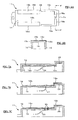
- is a plan view showing an upper case of a wireless communication device according to Embodiment 2 of the present invention as viewed from an upper side thereof;
- FIG. 2B
- is a cross-sectional view of the upper case unassembled, taken along line B-B of
FIG. 2A ; - FIG. 3A
- is a plan view showing an upper case of a wireless communication device according to Embodiment 3 of the present invention as viewed from an upper side thereof;
- FIG. 3B
- is a cross-sectional view of the upper case unassembled, taken along line C-C of
FIG. 3A ; - FIG. 4A
- is a bottom view showing an upper case of a wireless communication device according to Embodiment 4 of the present invention as viewed from an inner side thereof;
- FIG. 4B
- is a cross-sectional view of the upper case unassembled, taken along line D-D of
FIG. 4A ; - FIG. 5A
- is a bottom view showing an upper case of a wireless communication device according to Embodiment 5 of the present invention as viewed from an inner side thereof;
- FIG. 5B
- is a cross-sectional view of the upper case unassembled, taken along line E-E of
FIG. 5A ; - FIG. 6A
- is a bottom view showing an upper case of a wireless communication device according to Embodiment 6 of the present invention as viewed from an inner side thereof;
- FIG. 6B
- is a cross-sectional view of the upper case unassembled, taken along line F-F of
FIG. 6A ; - FIG. 7A
- is a cross-sectional view showing an embodiment in which a protruding
portion 29 that protrudes outwardly from a portion of atop panel 14 is formed and the short side portion of the L-shape of anantenna element portion 18a is disposed on the inner side of the protrudingportion 29; - FIG. 7B
- is a cross-sectional view showing an embodiment in which the protruding
portion 29 that protrudes outwardly from a portion of atop panel 14 is formed and the short side portion of the L-shape of theantenna element portion 18a is disposed on the outer side of the protrudingportion 29; - FIG. 7C
- is a cross-sectional view showing a case where the connection with an antenna cable is performed via through holes in the antenna arrangement same as that of
FIG. 7B ; - FIG. 8A
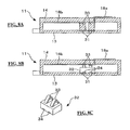
- is a cross-sectional view showing an embodiment in which an
antenna element 18 is directly connected to asubstrate 13 via capacitive coupling (C coupling)elements 30; - FIG. 8B
- is a cross-sectional view showing an embodiment in which the
antenna element 18 is directly connected to thesubstrate 13 via anelectrical connector 32; - FIG. 8C
- is a perspective view showing the
electrical connector 32; - FIG. 9A
- is a bottom view showing an inner side of an upper case illustrating a case where the
antenna element portion 18a and the antennaelement ground portion 18b partially overlap with each other; - FIG. 9B
- is a cross-sectional view showing the upper case unassembled, taken along line G-G of
FIG. 9A ; - FIG. 10
- is a perspective view showing an example of how to use in the case where a
connector 22 of awireless communication device 10 is provided at the side of thelong side panel 16; - FIG. 11
- is a cross-sectional view showing an embodiment in which the
antenna element portion 18a that is provided on the outer surface of thetop panel 14 is connected to the inner surface of thetop panel 14 via acapacitive coupling element 37; and - FIG. 12
- is a perspective view representing a conventional wireless communication device (dongle).
- A wireless communication device of the present invention includes: a housing of a rectangular parallelepiped shape that is constituted by a lower case and an upper case having an elongated top panel and side panels circumferentially-provided around the top panel; and a substrate having a connector for connecting with a mobile device and a communication electronic component provided inside the housing.
- In this wireless communication device, a pair of dipole antennas is formed in a sheet shape generally across an entire surface of the top panel of the upper case. In high-speed communication using the MIMO (Multiple Input Multiple Output) technique, the transmission and reception are performed simultaneously, and a synthesis is performed when receiving, thereby obtaining a wilder bandwidth.
- When used, the wireless communication device is placed on a flat surface with a top panel of the
lower case 12 facing downward and the top panel of theupper case 11 being placed horizontally and facing upward, while a USB cable connected to, for example, a USB terminal of a mobile device is connected to the connector of the wireless communication device. - Embodiments to be described below are different from each other in terms of the process of forming an
antenna element 18 on atop panel 14 of theupper case 11 constituting the housing.Embodiment 1 will be described in detail. In the following embodiments, however, only the points different from those of the other embodiments in a method for forming theantenna element 18 will be described. -
FIGS. 1A and 1B show awireless communication device 10 according toEmbodiment 1 of the present invention.FIG. 1A is a plan view showing anupper case 11 constituting a housing as viewed from an inner side thereof, andFIG. 1B is a cross-sectional view of theupper case 11, alower case 12, and asubstrate 13 unassembled, as viewed from the side surface. The external dimensions of thewireless communication device 10 are 23 mm in length, 46.5 mm in width (seeFIG. 1A ) and 13.5 mm in height (the height after theupper case 11 and thelower case 12 ofFIG. 1B are assembled together). The thickness of atop panel 14 is 1 mm. - As shown in
FIG. 1B , thewireless communication device 10 of the present invention includes a housing constituted by the hollowupper case 11 and the hollowlower case 12 attached to each other at portions ofshort side panels 15 andlong side panel 16. Each of theupper case 11 and thelower case 12 is of a generally rectangular parallelepiped shape, and thetop panel 14 and abottom panel 17 have the largest areas. - The
substrate 13 having thereon aconnector 22 for connecting with a mobile device and an electronic component such as an IC which enables wireless communications such as WiMAX communication is provided on an inner side of thelower case 12 so that theconnector 22 is exposed at theshort side panel 15. - An
antenna element 18 is formed in a sheet shape on an inner surface of thetop panel 14 of theupper case 11. Theupper case 11 and thelower case 12 are formed by molding a resin, and theantenna element 18 is made of a conductive metal, for example. Note that the "antenna element 18" used herein refers to both anantenna element portion 18a and an antennaelement ground portion 18b. - In
Embodiment 1, theantenna element portion 18a and the antennaelement ground portion 18b are first formed on a flexible printed circuit (hereinafter referred to as an "FPC") 19 in a sheet form, and the thus-obtained structure is then bonded to the inner surface of thetop panel 14 by means of an adhesive 20, as shown inFIG. 1B . - An
antenna cable 21 is connected to the bondedantenna element 18 such that acenter conductor 21 a of the antenna cable is soldered to theantenna element portion 18a and anet portion 21 b of the antenna cable is soldered to the antennaelement ground portion 18b. Thereafter, a connector of theantenna cable 21 is connected to the connector of thesubstrate 13, and theupper case 11, thelower case 12 and thesubstrate 13 are assembled to obtain thewireless communication device 10. Thewireless communication device 10 is used, for example, by connecting with a mobile device via aUSB cable 23 with theUSB cable 23 being connected to theconnector 22. - Various shape patterns can be used for the
antenna element 18. For example, theantenna element 18 may include two symmetrically-arranged, L-shapedantenna element portions 18a and two symmetrically-arranged, generally I-shaped antennaelement ground portions 18b as shown inFIG. 1A . A dipole antenna is formed by theantenna element portions 18a and antennaelement ground portions 18b in such an arrangement. - The
antenna element portions 18a and antennaelement ground portions 18b are respectively arranged close to the four corners of a rectangle which is a face of thetop panel 14 of a generally rectangular parallelepiped shape shown inFIG. 1A so that the two pairs of antennas are widely disposed generally across the entire surface of thetop panel 14. - In addition to this, by forming the
antenna element 18 on thetop panel 14 that has the largest area and is away from thesubstrate 13, it becomes possible to accommodate a wide frequency band with a high gain and to achieve further reductions in size and thickness. - Although the
top panel 14 is illustrated to have a completely flat surface inFIGS. 1A and 1B , the present invention is not limited thereto. By employing a technique in which a sheet of theFPC 19 with theantenna element 18 formed thereon is bonded to the inner side of thetop panel 14 of theupper case 11, even when theupper case 11 has thetop panel 14 of a curved shape, for example, the sheet of theFPC 19 with theantenna element 18 thereon can be bonded while being curved. Thus, the degree of freedom in design is increased. - The antenna performance can be further improved by forming a protruding
portion 29 that protrudes outwardly from a portion of thetop panel 14 and disposing the short side portion of the L-shape of theantenna element portion 18a on an inner side of the protrudingportion 29, so that theantenna element portion 18a can be further away from thesubstrate 13 by the height of the protrusion as shown inFIG. 7A . - The effective portion to be provided in the protruding
portion 29 is a portion furthest away from a portion connected to the antenna cable 21 (substrate connecting portion). In the embodiment shown inFIG. 7A , the short side portion of the L-shape of theantenna element portion 18a is provided in the protrudingportion 29. - The present invention is not limited to the case where the protruding
portion 29 is provided as inFIG. 7A . For example, the antenna performance can be further improved by reducing the thickness of a portion of thetop panel 14 within a range of the thickness thereof to form a depressed portion and by disposing the short side portion of the L-shape of theantenna element portion 18a in the depressed portion so that the portion of theantenna element portion 18a can be further away from thesubstrate 13 by the height of the depression. - Note that means to provide the
antenna element 18 on thetop panel 14 is not limited to the method in which theFPC 19 with theantenna element 18 thereon is bonded to thetop panel 14. Theantenna element 18 may be arranged on thetop panel 14 in the similar manner to that ofFIGS. 7A to 7C by using a plating process, integral molding, or the like, to be described later. - Moreover, by arranging the
antenna element portion 18a on one side of theFPC 19 and the antennaelement ground portion 18b on the other side thereof, and by using a material of a suitable dielectric constant for theFPC 19, the resonance frequency is decreased with theFPC 19, and the unfolded antenna length is shortened, thereby exhibiting the shortening effect. - Furthermore, as described in another embodiment, the
antenna element portion 18a and the antennaelement ground portion 18b which are arranged on different surfaces may be partially overlapped with each other as shown inFIG. 9A , thereby increasing the capacity thereof and thus achieving a wider bandwidth. - Although the sheet of the
FPC 19 with theantenna element 18 formed thereon is bonded to the inner side of thetop panel 14 of theupper case 11 inEmbodiment 1, the sheet of theFPC 19 with theantenna element 18 formed thereon may be bonded to the outer side of thetop panel 14 of theupper case 11 as shown inFIGS. 2A and 2B . Note that since Embodiment 2 is basically the same asEmbodiment 1, like elements to those ofEmbodiment 1 will be denoted by like reference numerals and the description thereof will be omitted. - In Embodiment 2, in order to connect the
antenna cable 21 to theantenna element 18, a throughhole 24 is formed running through theupper case 11 and theFPC 19, and thecable 21 is passed therethrough and soldered to theantenna element 18, for example, as shown inFIG. 2B . - The antenna effect is increased by forming the
antenna element 18 on the outer side of thetop panel 14 of theupper case 11 as in Embodiment 2 so that theantenna element 18 can be away from the substrate. - As shown in
FIG. 7B , the antenna performance can be further improved by forming the protrudingportion 29 that protrudes outwardly from a portion of thetop panel 14 and disposing the short side portion of the L-shape of theantenna element portion 18a on the outer side of the protrudingportion 29 so that the short side portion can be further away from thesubstrate 13 by the height of the protrusion. - The effective portion to be provided in the protruding
portion 29 is a portion furthest away from a portion connected to the antenna cable 21 (substrate connecting portion). In the embodiment shown inFIG. 7B , the short side portion of the L-shape of theantenna element portion 18a is provided at the protrudingportion 29. - In the case where the
antenna element 18 is formed on the outer side of thetop panel 14 as shown inFIG. 7B , throughholes 35 may be formed as shown inFIG. 7C , and theantenna element 18 may be connected to theantenna cable 21 at the inner side of thetop panel 14 via the through holes 35. - Although the sheet of the
FPC 19 with theantenna element 18 formed thereon is bonded to the inner side or outer side of thetop panel 14 of theupper case 11 inEmbodiment 1 or 2, theantenna element 18 may be integrally molded with theupper case 11 as shown inFIGS. 3A and 3B . Note that since Embodiment 3 is basically the same asEmbodiment 1, like elements to those ofEmbodiment 1 will be denoted by like reference numerals and the description thereof will be omitted. - In the
antenna element 18 shown inFIG. 3A , a portion thereof denoted by a solid line is disposed on the outer side of theupper case 11, and a portion thereof denoted by a broken line is disposed on the inner side of theupper case 11. At the boundary between the solid line and the broken line, the inner side portion of theantenna element 18 is connected to the outer side portion of the antenna element 18 (seeFIG. 3B ). - The
upper case 11 shown inFIGS. 3A and 3B can be fabricated, for example, by forming such abent antenna element 18 by molding in advance, and then burying the obtainedantenna element 18 in theupper case 11 in the process of molding theupper case 11. Note that when it is difficult to complete the integral molding process in a single step, the primary molding process may be performed to give a partially-finished product which is finished in the following secondary molding process. - The
wireless communication device 10 is fabricated by forming theupper case 11 as shown inFIGS. 3A and 3B , connecting the connector of theantenna cable 21 that is connected to theantenna element 18 with the connector of thesubstrate 13, and then assembling theupper case 11, thelower case 12 and thesubstrate 13. As a result, the portion of theantenna element portion 18a that is formed on the outer side of theupper case 11 can be further away from thesubstrate 13 by an amount equal to the thickness of thetop panel 14, thus increasing the antenna effect. - Since the
antenna element portion 18a can be further away from the substrate by an amount equal to the thickness of thetop panel 14 as described above, the distance between thesubstrate 13 and thetop panel 14 may be shortened. For example, as shown inFIG. 8A , theantenna element portion 18a and the antennaelement ground portion 18b can be directly connected toelectrodes 31 of thesubstrate 13 via capacitive coupling (C coupling)elements 30. Examples of the case using thecapacitive coupling element 30 include a case where a chip condenser is used and a case where the connection is made via a dielectric material. - The arrangement of the
antenna element 18 same as that ofFIGS. 3A and 3B can be obtained using theFPC 19. The antenna element can be similarly arranged by burying, in theupper case 11, theFPC 19 on which theantenna element 18 of a predetermined shape has been printed and which has been subjected to the bending process. - Alternatively, the
antenna element portion 18a and the antennaelement ground portion 18b may be directly connected to theelectrodes 31 of thesubstrate 13 via anelectrical connector 32 as shown inFIG. 8B . Theelectrical connector 32 includes, for example,contact portions 33 for contacting theantenna element portion 18a and the antennaelement ground portion 18b, andsubstrate connecting portions 34 electrically connected to thecontact portions 33 as shown inFIG. 8C . - The connection as shown in
FIG. 8A or 8B eliminates the need for using a coaxial cable, reduces the thickness of theupper case 11, and ensures the antenna performance. - Although a portion of the
antenna element portion 18a is disposed on the inner side of thetop panel 14 inFIG. 8A or 8B , theantenna element portion 18a may be disposed on the outer side of thetop panel 14 and pass through the inner surface of thetop panel 14 by providing a through hole whose inner wall is plated. Then, theantenna element portion 18a is connected to theelectrode 31 of thesubstrate 13 on the inner surface of thetop panel 14 using thecapacitive coupling element 30 or theelectrical connector 32. Then, the connection can be made without a cable, the antenna performance can be ensured, and the fabrication can be performed easily and inexpensively. - As shown in
FIGS. 9A and 9B , theantenna element portion 18a disposed on the outer side of thetop panel 14 may partially overlap in a planar view with the antennaelement ground portion 18b disposed on the inner side of thetop panel 14. As a result, the distance between theantenna element portion 18a and the antennaelement ground portion 18b in the thickness direction of thetop panel 14 is reduced, and the capacitance is thus increased. Therefore, it is possible to achieve the wider bandwidth. - Moreover, it is possible to suitably change the overlapping area of the
antenna element portion 18a and the antennaelement ground portion 18b or the position thereof on the planar surface of thetop panel 14, and to adjust the distance between theantenna element portion 18a and the antennaelement ground portion 18b in the thickness direction of thetop panel 14, thereby increasing the degree of freedom in the antenna design. - Note that in this case, the
antenna element portion 18a may be connected in advance with the antennaelement ground portion 18b using a coaxial cable, soldering and the like, and then integral molding can be performed as shown inFIGS. 9A and 9B . - As for the fabrication, the antenna
element ground portion 18b is provided with a hole slightly lager than the outer dimensions of thenet portion 21b of theantenna cable 21, theantenna cable 21 is passed through the hole, thecenter conductor 21 a is soldered to the lower surface of theantenna element portion 18a, and thenet portion 21b having passed through the hole is soldered to the antennaelement ground portion 18b. Integral molding with theupper case 11 in such an arrangement as shown inFIG. 9B can be then performed. - If a double mold process is performed wherein a dielectric material having a predetermined dielectric constant is molded between the
antenna element portion 18a and the antennaelement ground portion 18b in the primary molding process and theupper case 11 is completed in the secondary molding process by burying, in theupper case 11, theantenna element portion 18a and the antennaelement ground portion 18b with the dielectric material therebetween, the resonance frequency is decreased and the unfolded antenna length is shortened, thereby exhibiting the shortening effect. -
FIGS. 4A and 4B show awireless communication device 10 according to Embodiment 4 of the present invention.FIG. 4A is a bottom view showing theupper case 11 constituting a housing as viewed from an inner side thereof, andFIG. 4B is a cross-sectional view of theupper case 11 unassembled, as viewed from the side of thelong side panel 16. In Embodiment 4, thedielectric layer 25 is provided between theantenna elements 18. - As shown in
FIGS. 4A and 4B , thedielectric layer 25 is formed between theantenna element portion 18a and the antennaelement ground portion 18b by first forming theantenna element portion 18a on the inner side of theupper case 11 using a plating process, for example, then forming thedielectric layer 25 thereon across the entire inner surface of theupper case 11, and forming the antennaclement ground portion 18b on thedielectric layer 25 using a plating process, for example. - Note that although the plating process can be performed by suitably using masking or a laser, the Laser-Direct-Structuring (LSD) technique is favorable in that a plating process can be easily performed even on protruding or depressed surfaces with a laser. With this technique, the
antenna element portion 18a or the antennaelement ground portion 18b can be disposed on the protruding portion or depressed portion of theupper case 11, thereby making it possible to dispose theantenna element portion 18a further away from the above-described substrate. - The
wireless communication device 10 is fabricated by forming theupper case 11 as shown inFIGS. 4A and 4B , connecting the connector of theantenna cable 21 that is connected to theantenna element 18 with the connector of thesubstrate 13, and then assembling theupper case 11, thelower case 12 and thesubstrate 13. Note that thedielectric layer 25 is provided with asolder hole 26 for soldering. - By providing the
dielectric layer 25 between theantenna element portion 18a and the antennaelement ground portion 18b as described above, the wavelength shortening effect of the dielectric material reduces the effective area necessary for theantenna element 18, and a further reduction in size as a whole can be thus achieved. -
FIGS. 5A and 5B show awireless communication device 10 according to Embodiment 5 of the present invention.FIG. 5A is a bottom view showing theupper case 11 constituting a housing as viewed from an inner side thereof, andFIG. 5B is a cross-sectional view of theupper case 11 unassembled, as viewed from the side of theshort side panel 15. In Embodiment 5, theantenna element 18 is extended and bent so as to reach the side of thelong side panel 16. - As shown in
FIGS. 5A and 5B , when forming theantenna element portion 18a and the antennaelement ground portion 18b on the inner surface of thetop panel 14 of theupper case 11 using a plating process or the like, theantenna element portion 18a and the antennaelement ground portion 18b are extended and bent to reach the side of thelong side panel 16 so that antenna element bentportions - Although the
antenna element 18 is extended only to reach the side of thelong side panel 16 in the example shown inFIGS. 5A and 5B , it is also possible to extend theantenna element 18 to reach the side of theshort side panel 15. By extending theantenna element 18 to reach the side panel as described above, the side panel can be also utilized as the effective area of the antenna, thereby allowing for a further reduction in size as a whole. In the example shown inFIGS. 5A and 5B , it is possible to reduce the width of theshort side panel 15 as compared with that in other embodiments. - In Embodiment 5 described above, when forming the
antenna element portion 18a and the antennaelement ground portion 18b on the inner surface of thetop panel 14 of theupper case 11 using a plating process or the like, theantenna element portion 18a and the antennaelement ground portion 18b are respectively extended and bent to reach the side of thelong side panel 16 so that antenna element bentportions antenna element 18 is formed on the outer surface of thetop panel 14 of theupper case 11 as shown inFIGS. 6A and 6B , the antenna element bentportions - Note that regarding Embodiments 5 and 6, the method for forming the
antenna element 18 may be such that a conductive metal plate that has been subjected to a pressing process so as to achieve the arrangement as described above on theupper case 11 is integrally molded with theupper case 11 or such that theFPC 19 with the antenna element formed thereon that has been subjected to a bending process may be integrally molded with theupper case 11. - In the case where the
antenna element portion 18a is provided on the outer surface of thetop panel 14, theantenna element portion 18a is allowed to be drawn to the inner surface of thetop panel 14 by means using thecable 21 shown inFIGS. 2A and 2B , or means using the throughholes 35 shown inFIG. 7C . However, the present invention is not limited thereto. - For example, as shown in
FIG. 11 , acapacitive coupling element 37 may be provided inside thetop panel 14, and theantenna element portion 18a that is provided on the outer surface of thetop panel 14 may be virtually drawn to the inner surface of thetop panel 14 via thecapacitive coupling element 37. Thecapacitive coupling element 37 in this case may be buried in thetop panel 14 or may be fitted into a hole made through thetop panel 14. - Although the
connector 22 is provided at theshort side panel 15 inEmbodiments 1 to 7, the present invention is not limited thereto. Theconnector 22 may be provided at thelong side panel 16. If theconnector 22 is formed at the side of thelong side panel 16 and thewireless communication device 10 is connected to amobile device 36 via theUSB cable 22 having a predetermined length allowing for a bend of ± 90° or more, the use of thewireless communication device 10 is not limited to such a case that the top panel of theupper case 11 with the antenna element provided thereon is placed horizontally and facing the planar surface upwardly while the top panel of thelower case 12 is used as the bottom surface as inEmbodiments 1 to 7. - As shown in
FIG. 10 , thewireless communication device 10 can stand lengthwise when used with one of the twoshort side panels 15 being the bottom surface thereof. By using thewireless communication device 10 in such a manner, theantenna element 18 can be made to stand vertically, and one end of theantenna element portion 18a or the antennaelement ground portion 18b (a portion of the antenna element between the antenna element portion and the antenna element ground portion that is farthest away from the other) can be positioned high, thereby further improving the antenna sensitivity without using a particular kind of structure such as a conventional flip structure. Note that the end of theantenna element portion 18a is preferably positioned higher as shown inFIG. 10 so as to obtain a better antenna sensitivity. - Although the present invention has been described using a housing of a rectangular parallelepiped shape in
Embodiments 1 to 7 described above, the present invention is not limited thereto. The present invention can be applied also in a cylindrical housing with thetop panel 14 of a circular shape, for example. By forming theantenna element 18 on thetop panel 14 of the housing having the largest face, it becomes possible to achieve a smaller size and a smaller thickness while accommodating a wide frequency band with a high gain. - Although there are provided the two
antenna element portions 18a and the two antennaelement ground portions 18b inEmbodiments 1 to 7, the present invention is not limited thereto. The present invention is effective also in the case where oneantenna element portion 18a and one antennaelement ground portion 18b are disposed. - Patent Literature
- Patent Document 1:
- Japanese Translation of PCT International Application No.
2007-528057 - List of Reference Signs
- 11
- upper case
- 12
- lower case
- 13
- substrate
- 14
- top panel
- 15
- short side panel
- 16
- long side panel
- 17
- bottom panel
- 18
- antenna element
- 18a
- antenna element portion
- 18b
- antenna element ground portion
- 18c
- antenna element bent portion,
- 18d
- antenna element bent portion
- 19
- flexible printed circuit
- 20
- adhesive
- 21
- antenna cable
- 21a
- center conductor
- 21b
- net portion
- 22
- connector
- 23
- USB cable
- 24
- through hole
- 25
- dielectric layer
- 26
- solder hole
- 27
- dongle body
- 28
- antenna element
- 29
- protruding portion
- 30
- coupling element
- 31
- antenna electrode
- 32
- electrical connector
- 33
- contact portion
- 34
- substrate connecting portion
- 35
- through hole
- 36
- mobile device
- 37
- capacitive coupling element
Claims (20)
- A wireless communication device (10), comprising:- a housing; and- a substrate (13) having a connector (22) for connecting with a mobile device and a communication electronic component provided inside the housing,- the wireless communication device (10),characterized in that an antenna element (18) constituted by an antenna element portion (18a) and an antenna element ground portion (18b) is formed in a sheet shape generally across an entire surface of a top panel (14) of the housing.
- The device according to claim 1,
characterized in that the housing is of a rectangular parallelepiped shape constituted by a lower case (12) and an upper case (11) including a top panel (14) and side panels (15, 16) extending vertically from a circumference of the top panel (14) and adapted to accommodate the substrate (13). - The device (10) according to claim 1 or 2,
characterized in that the antenna element (18) is formed in a sheet shape generally across an entire outer surface of the top panel (14). - The device (10) according to claim 1 or 2,
characterized in that the antenna element (18) is formed in a sheet shape generally across an entire inner surface of the top panel (14). - The device (10) according to any one of claims 1 to 4,
characterized in that the antenna element (18) is disposed on a flexible printed circuit (19), and the flexible printed circuit (19) is provided on the outer surface or the inner surface of the top panel (14). - The device (10) according to claim 5,
characterized in that the flexible printed circuit (19) is further extended across the side panel (15, 16) and bonded thereto, so that the antenna element (18) is formed extending from the top panel (14) to any of an outer surface and an inner surface of the side panel (15, 16). - The device (10) according to claim 5,
characterized in that the antenna element portion (18a) is disposed on one side of the flexible printed circuit (19) formed by a predetermined dielectric material, and the antenna element ground portion (18b) is disposed on the other side of the flexible printed circuit (19). - The device (10) according to any one of claims 1 to 4,
characterized in that the antenna element (18) is integrally molded with the top panel (14), and the antenna element (18) is disposed on each of an inner side and an outer side of the top panel (14) at different positions in a thickness direction of the top panel (14). - The device (10) according to claim 8,
characterized in that the antenna element (18) is formed by punching and bending a conductive metal, and at least a portion of the antenna element (18) that is furthest away by planar distance among the antenna element portion (18a) and the antenna element ground portion (18b) is disposed on the outer side of the top panel (14). - The device (10) according to claim 8,
characterized in that the antenna element (18) and the top panel (14) are integrally molded and a predetermined dielectric material is fixed to one of the antenna element ground portion (18b) and the antenna element portion (18a) and the dielectric material is closely in contact with the other of the antenna element ground portion (18b) and the antenna element portion (18a). - The device (10) according to any one of claims 1 to 4,
characterized in that a dielectric layer (25) is disposed so as to be in contact with an upper surface of one of the antenna element portion (18a) and the antenna element ground portion (18b) and a lower surface of the other of the antenna element portion (18a) and the antenna element ground portion (18b), whereby the dielectric layed (25) is provided between the antenna element portion (18a) and the antenna element ground portion (18b). - The device (10) according to any one of claims 1 to 4,
characterized in that, wherein the antenna element (18) is formed by subjecting the top panel (14) of the upper case (11) to a plating process. - The device (10) according to claim 12, characterized in that a portion of the antenna element (18) formed by the plating process is extended from the top panel (14) to the side panel (15, 16).
- The device (10) according to any one of claims 1 to 5, 8, 11 and 12,
characterized in that a protruding portion (29) is provided in the top panel (14) by outwardly deforming a portion of the outer surface of the top panel (14), and at least a portion of the antenna element (18) that is furthest away from among the antenna element portion (18a) and the antenna element ground portion (18b) is provided in the protruding portion (29). - The device (10) according to any one of claims 1, 2, 4, 5, 8, 11 and 12,
characterized in that a depressed portion is provided by depressing a portion of the inner surface of the top panel (14), and at least a portion of the antenna element (18) that is furthest away from among the antenna element portion (18a) and the antenna element ground portion (18b) is provided in the depressed portion. - The device (10) according to any one of claims 1, 2, 5, 8, 11 and 12, characterized in that the antenna element portion (18a) and the antenna element ground portion (18b) partially overlap with each other in a planar view.
- The device (10) according to any one of claims 1, 2, 5, 8, 11 and 12,
characterized in that the antenna element (18) is connected to an antenna electrode (31) provided in the substrate (13) via a capacitive coupling element (30). - The device (10) according to any one of claims 1, 2, 5, 8, 11 and 12,
characterized in that the antenna element (18) is connected to an antenna electrode (31) provided in the substrate (13) via an electrical connector (32). - The device (10) according to any of claims 1 to 18,
characterized in that the housing is of a rectangular parallelepiped shape and has a quadrangular top panel (14) and a quadrangular bottom panel (17) parallel to each other and four side panels (15, 16) vertically extending from a circumference of the top panel (14);
in that the antenna element (18) is provided on the top panel (14); in that the connector (22) is provided on one of the side panels (15, 16); and
in that the antenna element (18) is positioned horizontally when the bottom panel (17) is placed at a bottom surface, and the antenna element (18) is positioned vertically when another one of the side panels (15, 16) perpendicular to the side panel (15, 16) at which the connector (22) is provided is placed at a bottom surface, with the connector (22) being fitted into a counterpart connector connected to a mobile device via a cable (23). - A method of using a wireless communication device (10) including:a housing of a rectangular parallelepiped shape having a quadrangular top panel (14) and a quadrangular bottom panel (17) parallel to each other and four side panels (15, 16) vertically extending from a circumference of the top panel (14);a substrate (13) having a connector (22) for connecting with a mobile device and a communication electronic component provided inside the housing so that the connector (22) is provided on one of the four side panels (15, 16); andan antenna element (18) constituted by an antenna element portion (18a) and an antenna element ground portion (18b) being formed in a sheet shape generally across the top panel (14),the method of using the wireless communication device (10) being characterized by using the wireless communication device (10) in an upright position such that one of the side panels (15, 16) perpendicular to the side panel (15, 16) at which the connector (22) is provided is placed as a bottom surface with the connector (22) being fitted into a counterpart connector connected to a mobile device via a cable (23).
Applications Claiming Priority (1)
| Application Number | Priority Date | Filing Date | Title |
|---|---|---|---|
| JP2009205298A JP2011061251A (en) | 2009-09-04 | 2009-09-04 | Radio communication apparatus, and method for using the same |
Publications (1)
| Publication Number | Publication Date |
|---|---|
| EP2312688A2 true EP2312688A2 (en) | 2011-04-20 |
Family
ID=43640124
Family Applications (1)
| Application Number | Title | Priority Date | Filing Date |
|---|---|---|---|
| EP20100173856 Withdrawn EP2312688A2 (en) | 2009-09-04 | 2010-08-24 | Wireless communication device and method of using the same |
Country Status (2)
| Country | Link |
|---|---|
| EP (1) | EP2312688A2 (en) |
| JP (1) | JP2011061251A (en) |
Cited By (2)
| Publication number | Priority date | Publication date | Assignee | Title |
|---|---|---|---|---|
| US9420735B2 (en) | 2011-08-12 | 2016-08-16 | Sharp Kabushiki Kaisha | Structure and structure manufacturing method |
| CN108199140A (en) * | 2018-02-24 | 2018-06-22 | 深圳市道通智能航空技术有限公司 | Remote controler |
Families Citing this family (2)
| Publication number | Priority date | Publication date | Assignee | Title |
|---|---|---|---|---|
| JP4861462B2 (en) * | 2009-09-30 | 2012-01-25 | Smk株式会社 | Wireless communication device |
| JP6236377B2 (en) * | 2014-11-26 | 2017-11-22 | 京セラ株式会社 | Antenna structure and electronic device |
Citations (1)
| Publication number | Priority date | Publication date | Assignee | Title |
|---|---|---|---|---|
| JP2007528057A (en) | 2004-01-29 | 2007-10-04 | コーニンクレッカ フィリップス エレクトロニクス エヌ ヴィ | Guest dongle and method of connecting guest device to wireless home network |
Family Cites Families (5)
| Publication number | Priority date | Publication date | Assignee | Title |
|---|---|---|---|---|
| JP2705392B2 (en) * | 1991-09-04 | 1998-01-28 | 日本電気株式会社 | Portable radio |
| JPH0993029A (en) * | 1995-09-21 | 1997-04-04 | Matsushita Electric Ind Co Ltd | Antenna device |
| JP4240977B2 (en) * | 2002-09-30 | 2009-03-18 | 大日本印刷株式会社 | SIM holder with USB interface and SIM |
| JP4754601B2 (en) * | 2005-01-31 | 2011-08-24 | 富士通コンポーネント株式会社 | Antenna device |
| JP4756020B2 (en) * | 2007-09-25 | 2011-08-24 | 株式会社東芝 | Housing, method for manufacturing the same, and electronic device |
-
2009
- 2009-09-04 JP JP2009205298A patent/JP2011061251A/en active Pending
-
2010
- 2010-08-24 EP EP20100173856 patent/EP2312688A2/en not_active Withdrawn
Patent Citations (1)
| Publication number | Priority date | Publication date | Assignee | Title |
|---|---|---|---|---|
| JP2007528057A (en) | 2004-01-29 | 2007-10-04 | コーニンクレッカ フィリップス エレクトロニクス エヌ ヴィ | Guest dongle and method of connecting guest device to wireless home network |
Cited By (4)
| Publication number | Priority date | Publication date | Assignee | Title |
|---|---|---|---|---|
| US9420735B2 (en) | 2011-08-12 | 2016-08-16 | Sharp Kabushiki Kaisha | Structure and structure manufacturing method |
| CN108199140A (en) * | 2018-02-24 | 2018-06-22 | 深圳市道通智能航空技术有限公司 | Remote controler |
| WO2019161673A1 (en) * | 2018-02-24 | 2019-08-29 | 深圳市道通智能航空技术有限公司 | Remote control |
| CN108199140B (en) * | 2018-02-24 | 2020-03-24 | 深圳市道通智能航空技术有限公司 | Remote controller |
Also Published As
| Publication number | Publication date |
|---|---|
| JP2011061251A (en) | 2011-03-24 |
Similar Documents
| Publication | Publication Date | Title |
|---|---|---|
| JP5162012B1 (en) | ANTENNA DEVICE AND ELECTRONIC DEVICE HAVING THE ANTENNA DEVICE | |
| US20220255238A1 (en) | Antenna module and electronic device | |
| US9917357B2 (en) | Antenna system | |
| US8339322B2 (en) | Compact multi-band antennas | |
| US9136590B2 (en) | Electronic device provided with antenna device | |
| US7126547B2 (en) | Antenna module and electronic apparatus having the same | |
| US20100141536A1 (en) | Antenna | |
| US20040196190A1 (en) | Method for fabrication of miniature lightweight antennas | |
| CN102142599B (en) | For the built-in aerial of portable terminal and the portable terminal including it | |
| US8390523B2 (en) | Planar inverted-F antenna and wireless network device having the same | |
| KR20090133072A (en) | Antenna which is formed as a single body with printed circuit board | |
| US20140049431A1 (en) | Multi-band antenna | |
| EP2312688A2 (en) | Wireless communication device and method of using the same | |
| US9024820B2 (en) | Miniature antenna | |
| CN109037908B (en) | Antenna system of mobile terminal and mobile terminal | |
| CN101677148A (en) | Multifrequency antenna | |
| US20100238076A1 (en) | Printed antenna with improved mounting structure and electronic apparatus using the same | |
| JP4955047B2 (en) | High frequency coupler | |
| US20090303151A1 (en) | Low profile gps antenna assembly | |
| KR102046549B1 (en) | A internal antenna of portable terminal processing transaction information and a portable terminal comprising it | |
| US8368600B2 (en) | Dual-band antenna and wireless network device having the same | |
| JP2009124397A (en) | Antenna device and radio unit | |
| JP2006108830A (en) | Antenna system, radio communication equipment, and manufacturing method of antenna system | |
| JP7405862B2 (en) | Antenna equipment and wireless communication equipment | |
| TWI328310B (en) | Internal antenna for mobile device |
Legal Events
| Date | Code | Title | Description |
|---|---|---|---|
| PUAI | Public reference made under article 153(3) epc to a published international application that has entered the european phase |
Free format text: ORIGINAL CODE: 0009012 |
|
| AK | Designated contracting states |
Kind code of ref document: A2 Designated state(s): AL AT BE BG CH CY CZ DE DK EE ES FI FR GB GR HR HU IE IS IT LI LT LU LV MC MK MT NL NO PL PT RO SE SI SK SM TR |
|
| AX | Request for extension of the european patent |
Extension state: BA ME RS |
|
| STAA | Information on the status of an ep patent application or granted ep patent |
Free format text: STATUS: THE APPLICATION HAS BEEN WITHDRAWN |
|
| 18W | Application withdrawn |
Effective date: 20120730 |