EP2312632A1 - System for processing analog-type electrical signals with low noise driving device - Google Patents
System for processing analog-type electrical signals with low noise driving device Download PDFInfo
- Publication number
- EP2312632A1 EP2312632A1 EP20100176594 EP10176594A EP2312632A1 EP 2312632 A1 EP2312632 A1 EP 2312632A1 EP 20100176594 EP20100176594 EP 20100176594 EP 10176594 A EP10176594 A EP 10176594A EP 2312632 A1 EP2312632 A1 EP 2312632A1
- Authority
- EP
- European Patent Office
- Prior art keywords
- terminal
- driving
- control
- analog
- switch module
- Prior art date
- Legal status (The legal status is an assumption and is not a legal conclusion. Google has not performed a legal analysis and makes no representation as to the accuracy of the status listed.)
- Withdrawn
Links
- 238000012545 processing Methods 0.000 title claims description 55
- 230000007704 transition Effects 0.000 claims abstract description 44
- 238000012546 transfer Methods 0.000 claims description 6
- 238000010586 diagram Methods 0.000 description 6
- 101100072644 Saccharomyces cerevisiae (strain ATCC 204508 / S288c) INO2 gene Proteins 0.000 description 4
- 101100454372 Saccharomyces cerevisiae (strain ATCC 204508 / S288c) LCB2 gene Proteins 0.000 description 4
- 101100489624 Saccharomyces cerevisiae (strain ATCC 204508 / S288c) RTS1 gene Proteins 0.000 description 4
- 238000004377 microelectronic Methods 0.000 description 4
- 230000036039 immunity Effects 0.000 description 3
- 230000003094 perturbing effect Effects 0.000 description 3
- 230000015556 catabolic process Effects 0.000 description 2
- 238000006243 chemical reaction Methods 0.000 description 2
- 238000006731 degradation reaction Methods 0.000 description 2
- 238000012986 modification Methods 0.000 description 2
- 230000004048 modification Effects 0.000 description 2
- 230000006978 adaptation Effects 0.000 description 1
- 230000003321 amplification Effects 0.000 description 1
- 238000013459 approach Methods 0.000 description 1
- 230000001934 delay Effects 0.000 description 1
- 230000003111 delayed effect Effects 0.000 description 1
- 230000001419 dependent effect Effects 0.000 description 1
- 230000009977 dual effect Effects 0.000 description 1
- 238000005516 engineering process Methods 0.000 description 1
- 230000002401 inhibitory effect Effects 0.000 description 1
- 238000005259 measurement Methods 0.000 description 1
- 238000003199 nucleic acid amplification method Methods 0.000 description 1
- 238000004321 preservation Methods 0.000 description 1
- 238000005070 sampling Methods 0.000 description 1
- 238000000638 solvent extraction Methods 0.000 description 1
- 239000002699 waste material Substances 0.000 description 1
Images


Classifications
-
- H—ELECTRICITY
- H03—ELECTRONIC CIRCUITRY
- H03K—PULSE TECHNIQUE
- H03K17/00—Electronic switching or gating, i.e. not by contact-making and –breaking
- H03K17/16—Modifications for eliminating interference voltages or currents
- H03K17/161—Modifications for eliminating interference voltages or currents in field-effect transistor switches
- H03K17/162—Modifications for eliminating interference voltages or currents in field-effect transistor switches without feedback from the output circuit to the control circuit
-
- H—ELECTRICITY
- H03—ELECTRONIC CIRCUITRY
- H03M—CODING; DECODING; CODE CONVERSION IN GENERAL
- H03M1/00—Analogue/digital conversion; Digital/analogue conversion
- H03M1/06—Continuously compensating for, or preventing, undesired influence of physical parameters
- H03M1/08—Continuously compensating for, or preventing, undesired influence of physical parameters of noise
- H03M1/0845—Continuously compensating for, or preventing, undesired influence of physical parameters of noise of power supply variations, e.g. ripple
-
- H—ELECTRICITY
- H03—ELECTRONIC CIRCUITRY
- H03M—CODING; DECODING; CODE CONVERSION IN GENERAL
- H03M1/00—Analogue/digital conversion; Digital/analogue conversion
- H03M1/12—Analogue/digital converters
-
- H—ELECTRICITY
- H03—ELECTRONIC CIRCUITRY
- H03M—CODING; DECODING; CODE CONVERSION IN GENERAL
- H03M1/00—Analogue/digital conversion; Digital/analogue conversion
- H03M1/66—Digital/analogue converters
Definitions
- the present invention relates to (electronic and/or micro-electronic) systems for the processing of analog-type electrical signals by means of the use of an analog circuitry and a digital circuitry, and in particular to a processing system of analog electrical signal according to the preamble of claim 1.
- a switch module In a processing (electronic and/or micro-electronic) system of analog-type electrical signals (hereinafter, for brevity's sake simply being referred to as analog signals), a switch module (switch) is typically employed, in particular applications, which is capable of enabling and inhibiting the transfer of an analog signal from a source module to a user module.
- the switch module is employed, as it is known, for the sampling function, by storing the analog signal value while the switch module results to be in the so-called "off" state.
- the switch module is also employed for the transfer of an analog signal towards an amplification stage, in predetermined time instants in which the same results to be in the so-called "on" state.
- a switch module operating on analog signals is driven by a corresponding control digital circuitry, having the task to generate control logic signals of the switch module and to provide to it, through a driving device, a driving electrical signal, on the basis of the above-mentioned control logic signals, to allow the opening (state “off”) or the closure (state “on”) of the switch module.
- Such driving device has the drawback of further perturbing the analog signal on which the switch module operates, adding noise and/or distortion to it, even in a significant amount.
- such system usually comprises two different types of it: a so-called “analog supply” circuitry, to which the system analog circuitry is electrically connected; and a so-called “digital supply” circuitry, to which the system digital circuitry is electrically connected.
- the "analog" supply is capable of providing, in a plurality of analog supply terminals, a first and a second analog supply potentials
- the "digital" supply is capable of providing, in a plurality of digital supply terminals, a first and a second digital supply potentials.
- Such first supply potentials can originate from, or coincide with, a first external supply potential, having a same nominal value one to the other.
- second supply potentials can originate from, or coincide with, a second external supply potential, having a same nominal value one to the other.
- first and second external supply potentials can be, for example, obtained from a battery.
- the "real" instantaneous values of such supply potentials can vary, departing from the nominal value.
- the digital supply is usually characterized by a higher "switch noise", associated to the switching operations of the digital components connected thereto.
- the availability of two supply circuitries is a compromise that is usually adopted among the availability of an individual supply circuitry, that would lead to a degraded performance mainly due to excessive undesired mutual influences determined by the different operating modes of the digital components and the analog components, and the availability of a number of different supply circuitries, to which single subsystems of the system would refer, which would improve the performance by minimizing the mutual influences, but would lead to unacceptable costs and space waste.
- the switch module control circuitry is connected to the digital supply.
- the corresponding driving device results to be connected to the digital supply, which constitutes the last control circuitry component before the switch module, and which directly interacts with the same switch module through said driving electrical signal.
- the driving device connected to the digital supply, has the drawback that it transfers at least partially on the switch module, and therefore on the analog signal on which it operates, the switch noise that is present on the digital supply. Particularly, such noise is present both in the periods in which the switch module is “on” and in those in which it is “off".
- a known solution to cope with such drawback is the use of a driving device that is connected to the analog supply (which, as it is known, is already available) instead of being connected to the digital supply.
- the object of the present invention is to devise and provide an improved system for the processing of analog electrical signals employing a driving device that allows to at least partially obviate the drawbacks described above with reference to the prior art.
- FIG. 1 a processing system of analog electrical signals is now described, indicated on the whole by the reference numeral 100, according to an example of the present invention.
- processing system of an analog electrical signals is meant an electronic and/or micro-electronic system, preferably manufactured by integrated technology (on "chip"), designed to carry out on such signals, by the use of an analog circuitry and a digital circuitry, one of more functions and/or operations, per se known to those of ordinary skill in the art, such as, for example, switching, signal transfer, analog-to-digital conversion, digital-to-analog conversion, and so on.
- the processing system 100 comprises a source module 300 of an analog electrical signal SA, hereinafter also simply analog signal.
- the processing system 100 further comprises a user module 400, suitable to receive, on request, the analog signal SA generated by the source module 300.
- the type of the source module 300 and of the user module 400 depends on the type of functions and/or operations that are carried out by the processing system 100.
- the processing system 100 further comprises a switch module 200, per se known, operatively connected between the source module 300 and the user module 400.
- the switch 200 comprises an input terminal 201 arranged to receive in input the analog signal SA, and an output terminal 202, to provide the analog signal SA to the user module 400, when required.
- the switch module 200 results to be so configured as to assume a first or a second states, in order to enable and inhibit, respectively, the transfer of the analog signal SA from the source module 300 to the user module 400, on the basis of a driving electrical signal SP (for brevity's sake hereinafter also referred to as driving signal), that will be described below.
- a driving electrical signal SP for brevity's sake hereinafter also referred to as driving signal
- the switch module 200 in the first state (also referred to as “switched on”, or “on”), the switch module 200 behaves as a closed switch; in the second state (also referred to as “switched off”, or “off”), the switch module 200 behaves as an open switch.
- the analog signal that is present on the output terminal 202 is identified by the reference SA'.
- the analog signal SA' is ideally equal to the analog signal SA when the switch module 200 assumes the first state, and it is equal to 0 (null signal) when the switch module 200 assumes the second state.
- such analog signal SA' departs from the above-mentioned ideal trend, because of the noise or of other disturbance types.
- the processing system 100 further comprises a driving device 500 of the switch module 200.
- the driving device 500 results to be so configured as to drive, on the basis of the driving signal SP, a control terminal TC which the switch module 200 is provided with, so as to allow it to assume the first or the second state and to carry out a first driving transition type (hereinafter for brevity's sake also referred to as "first driving transition”) from the first state to the second state, and a second driving transition type (hereinafter for brevity's sake also referred to as "second driving transition”) from the second state to the first state.
- first driving transition type hereinafter for brevity's sake also referred to as "first driving transition
- second driving transition a second driving transition type
- the first and the second transition types are intrinsically associated to the dynamic operation of the switch module 200.
- each specific occurrence of one of such driving transitions occurs in a time interval that is associated to the above-mentioned transition, within which the transition itself takes place.
- Such time interval usually has a short duration compared to the duration of the successive "on” or “off” state of the switch module 200.
- the time interval associated to a driving transition can also be regarded as a "fraction" of the "on” state or the "off” state of the switch module 200.
- driving device 500 further comprises a driving device 500 control module 510 (hereinafter, for brevity's sake, control module), so configured as to generate a plurality of driving control signals SCP, which will be described herein below, on the basis of one or more system control signals SCS.
- control module 510 hereinafter, for brevity's sake, control module
- the driving device 500 further comprises a driving stage 520 operatively interposed between the control module 510 and the switch module 200.
- the driving stage 520 results to be configured to receive the plurality of control signals SCP from the control module 510 and to generate, on the basis of said plurality, the driving signal SP.
- the driving stage 520 will be described in more detail herein below, in some embodiments thereof, with particular reference to Figs. 2 and 4 .
- the processing system 100 further comprises a system control digital circuitry 600, arranged to generate, inter alia, one or more system control signals SCS intended to control, through the control module 510, the driving stage 520, and to accordingly determine the operation of the switch module 200.
- the system control digital circuitry 600 per se known, comprises, for example, a plurality of logical ports and/or components, and can vary depending on the type of the processing system 100 for which it is designed.
- the processing system 100 further comprises a first reference terminal T1 and a second reference terminal T2 associated, respectively, to a first reference potential V1 and a second reference potential V2.
- V1, V2 advantageously have a high immunity level compared to disturbances related to the switching of the digital circuitry components with which the processing system 100 is provided.
- the processing system 100 further comprises a third reference terminal T3 and a fourth reference terminal T4 associated, respectively, to a third reference potential V3 and a fourth reference potential V4.
- V3, V4 are advantageously chosen so as to result to be electrically distinct, respectively, from the first and the second reference potentials (V1, V2).
- the processing system 100 further comprises an analog circuitry supply circuitry 10, arranged to provide a first and a second analog supply potentials (VA1, VA2), for example, on corresponding analog supply terminals (TA1, TA2).
- VA1, VA2 analog supply potentials
- TA1, TA2 analog supply terminals
- the source module 300 and the user module 400 are operatively connected, in order to be supplied, to the analog supply terminals TA1, TA2. It has to be further noticed that, usually, other analog circuitry components, with which the processing system 100 can be provided (not shown in the Figure), whether they are integrated or not in the same chip of the analog supply circuitry 10 and/or of the other processing system 100 subsystems, can be operatively connected to the analog supply terminals TA1, TA2.
- the first and the second reference terminals T1, T2 respectively coincide with the analog supply terminals TA1, TA2.
- the first and the second reference potentials V1, V2 respectively coincide with the analog supply potentials VA1, VA2.
- analog supply potentials VA1 and VA2 usually have, as required for the reference potentials V1 and V2, a high immunity level compared to the disturbances related to the switching of the processing system 100 digital circuitry components.
- the processing system 100 further comprises a digital circuitry supply circuitry 20, arranged to provide a first digital supply potential VD1 and a second digital supply potential VD2, for example, on respective digital supply terminals TD1, TD2. It shall be further noticed that other digital circuitry components which the processing system 100 can be provided with (not shown in the Figure), whether they are integrated or not in the same chip of the digital supply circuitry 20 and/or of the other processing system 100 subsystems, can be usually operatively connected to the analog supply terminals TD1, TD2.
- the digital control circuitry 600 and the control module 510 are operatively connected, in order to be supplied, to the terminals TD1 and TD2.
- analog circuitry supply circuitry 10 and to the digital circuitry supply circuitry 20 it has to be observed that, according to different embodiments of the present invention, they can be integrated in the same chip that houses the circuitries which they supply, or they can be in one or more different chips.
- the third and the fourth reference potentials V3, V4 respectively coincide with the digital supply potentials VD1, VD2.
- the digital supply potentials VD1, VD2, as required for the reference potentials V3, V4, usually result to be electrically distinct from the first and the second reference potentials (V1, V2), respectively.
- VA1, VA2 nominal values are usually equal to the digital supply potentials (VD1, VD2) nominal values, respectively, while the corresponding real and instantaneous values can differ from one another, since each of them can vary in time, because of several non-idealities (for example, noise).
- the driving stage 520 results to be operatively connected both to the pair composed of the first and the second reference terminals (T1, T2) and to the pair composed of the third and the fourth reference terminals (T3, T4) .
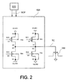
- the driving stage 520 is now described, according to an embodiment example. It is pointed out that, for clarity of description, the control module 510, operatively connected to the driving stage 520, as already illustrated before, to provide it with the plurality of driving control signals SCP, and the switch module 200 driven by the driving stage 520 through the control terminal TC, already introduced before, are schematically illustrated in Fig. 2 .
- the driving stage 520 comprises a first transistor TR1, for example, of the P-channel MOS type, provided with: a first source terminal S1 electrically connected to the first reference potential V1, i.e., to the analog supply potential VA1; a first gate terminal G1 operatively connected to the control module 510 to receive in input a first control signal SC1 belonging to the plurality of driving control signals SCP; a first drain terminal D1, operatively connected to the control terminal TC of the switch module 200.
- a first transistor TR1 for example, of the P-channel MOS type, provided with: a first source terminal S1 electrically connected to the first reference potential V1, i.e., to the analog supply potential VA1; a first gate terminal G1 operatively connected to the control module 510 to receive in input a first control signal SC1 belonging to the plurality of driving control signals SCP; a first drain terminal D1, operatively connected to the control terminal TC of the switch module 200.
- the driving stage 520 further comprises a second transistor TR2, for example, of the N-channel MOS type, provided with: a second drain terminal D2 connected to the first drain terminal D1 of the first transistor TR1, and, consequently, to the control terminal TC of the switch module 200; a second gate terminal G2 operatively connected to the control module 510 to receive in input a second control signal SC2 belonging to the plurality of driving control signals SCP; a second source terminal S2, electrically connected to the second reference potential V2, i.e., to the analog supply potential VA2.
- a second transistor TR2 for example, of the N-channel MOS type, provided with: a second drain terminal D2 connected to the first drain terminal D1 of the first transistor TR1, and, consequently, to the control terminal TC of the switch module 200; a second gate terminal G2 operatively connected to the control module 510 to receive in input a second control signal SC2 belonging to the plurality of driving control signals SCP; a second source terminal S2, electrically connected to the second reference potential V2,
- the driving stage 520 further comprises a third transistor TR3, for example, of the P-channel MOS type, provided with: a third source terminal S3 electrically connected to the third reference potential V3, i.e., to the digital supply potential VD1; a third gate terminal G3 operatively connected to the control module 510 to receive in input a third control signal SC3 belonging to the plurality of driving control signals SCP; a third drain terminal D3, also being operatively connected to the control terminal TC of the switch module 200, as well as to the first drain terminal D1 of the first transistor TR1 and to the second drain terminal D2 of the second transistor TR2.
- a third transistor TR3 for example, of the P-channel MOS type, provided with: a third source terminal S3 electrically connected to the third reference potential V3, i.e., to the digital supply potential VD1; a third gate terminal G3 operatively connected to the control module 510 to receive in input a third control signal SC3 belonging to the plurality of driving control signals SCP; a third drain
- the driving stage 520 further comprises a fourth transistor TR4, for example, of the N-channel MOS type, provided with: a fourth drain terminal D4 also operatively connected to the control terminal TC of the switch module 200, as well as to the third drain terminal D3 of the third transistor TR3, to the first drain terminal D1 of the first transistor TR1 and to the second drain terminal D2 of the second transistor TR2; a fourth gate terminal G4 operatively connected to the control module 510 to receive in input a fourth control signal SC4 belonging to the plurality of driving control signals SCP; a fourth source terminal S4 electrically connected to the fourth reference potential V4, i.e., to the digital supply potential VD2.
- a fourth transistor TR4 for example, of the N-channel MOS type, provided with: a fourth drain terminal D4 also operatively connected to the control terminal TC of the switch module 200, as well as to the third drain terminal D3 of the third transistor TR3, to the first drain terminal D1 of the first transistor TR1 and to the second drain terminal D2 of the second
- the driving stage 520 configuration ( Fig. 2 ) is such that, according to the switching on or off of the first transistor TR1, the second transistor TR2, the third transistor TR3, and the fourth transistor TR4, on the basis of the plurality of driving control signals SCP provided by the control module 510, the control terminal TC can be operatively connected to the first reference potential V1 (i.e., to the analog supply potential VA1), the second reference potential V2 (i.e., the analog supply potential VA2), the third reference potential V3 (i.e., the digital supply potential VD1), or the fourth reference potential V4 (i.e., the digital supply potential VD2).
- the first reference potential V1 i.e., to the analog supply potential VA1
- the second reference potential V2 i.e., the analog supply potential VA2
- the third reference potential V3 i.e., the digital supply potential VD1
- the fourth reference potential V4 i.e., the digital supply potential VD2
- the control module 510 is configured so that the third control signal SC3 is at a high logical level ("1"). It results that the third transistor TR3 is in the “switched off” condition and it behaves as an "open switch” between the respective source S3 and drain D3 terminals.
- the control module 510 is further configured so that the fourth control signal SC4 is at a low logical level ("0"). This implies that the fourth transistor TR4 is in the “switched off” condition and acts as an "open switch” between the respective source S4 and drain D4 terminals.
- control module 510 is configured so that the second control signal SC2 is at a low logical level ("0"). This implies the switching off of the second transistor TR2, which behaves as an "open switch", between the respective source S2 and drain D2 terminals.
- the control module 510 is configured so that the first control signal SC1 is at a low logical level ("0"). This implies that the first transistor TR1 is in the "switch on” condition and allows the electric connection between the respective source S1 and drain D1 terminals. Accordingly, the control terminal TC of the switch module 200, operatively connected to the first drain terminal D1, is electrically connected also to the first source terminal S1, therefore resulting to be electrically connected to the first reference potential V1, i.e., to the analog supply potential VA1.
- the first reference potential V1 has such a value as to correspond to a "high” logical level ("1"). Therefore, in the described configuration, also the driving signal SP, which is present at the control terminal TC of the switch module 200, results to be corresponding to a "high” logical level, with which it imposes the first state ("on”) of the switch module 200.
- the control module 510 results to be configured so that the third control signal SC3 is maintained to a high logical level ("1"); the second control signal SC2 is maintained to a low logical level ("0"); the first control signal SC1 is brought to a high logical level ("1"), in which the first transistor TR1 electrically disconnects the first drain terminal D1, and accordingly the control terminal TC, from the first source terminal S1, and therefore from the first reference potential V1; the fourth control signal SC4 is brought to a high logical level ("1"), in which the fourth transistor TR4 electrically connects the fourth drain terminal D4, and accordingly the control terminal TC, to the fourth source terminal S4, and therefore to the fourth reference potential V4, i.e., to the digital supply potential VD2.
- the transistor TR1 behaves as an "open switch”, while the transistor TR4 behaves as a "closed switch”.
- the fourth reference potential V4 has such a value as to correspond to a "low” logical level ("0"). Therefore, the driving signal SP present at the control terminal TC passes, during the first transition, from a "high” logical level to a “low” logical level, with which it imposes the corresponding transition from the first state “on” to the second state “off” to the switch module 200.
- the control module 510 is configured so that the third control signal SC3 is maintained to a high logical level ("1"); the first control signal SC1 is maintained to a high logical level ("1"). Furthermore, the control module 510 is configured so that the fourth control signal SC4 is brought to a "low” logical level ("0"), in which the fourth transistor TR4 electrically disconnects the fourth drain terminal D4, and accordingly the control terminal TC, from the fourth source terminal S4, and therefore from the fourth reference potential V4, i.e., from the digital supply potential VD2.
- control module 510 is configured so that the second control signal SC2 is brought to a "high" logical level ("1") in which the second transistor TR2 electrically connects the second drain terminal D2, and accordingly the control terminal TC, to the second source terminal S2, and therefore to the second reference potential V2, i.e., to the analog supply potential VA2.
- the fourth transistor TR4 behaves as an "open switch", while the second transistor TR2 behaves as a "closed switch”.
- the second reference potential V2 has such a value as to correspond to a "low” logical level ("0"). Therefore, in the described configuration, also the driving signal SP present at the control terminal TC of the switch module 200 results to be corresponding to a "low” logical level, with which it imposes the second state ("off") of the switch module 200.
- the control module 510 is configured so that the first control signal SC1 is maintained at a high logical level ("1"); the fourth control signal SC4 is maintained at a low logical level ("0"); the second control signal SC2 is brought to a low logical level ("0"), in which the second transistor TR2 electrically disconnects the second drain terminal D2, and accordingly the control terminal TC, from the second source terminal S2, and therefore from the second reference potential V2, i.e., from the analog supply potential VA2; the third control signal SC3 is brought to a low logical level ("0"), in which the third transistor TR3 electrically connects the third drain terminal D3, and accordingly the control terminal TC, to the third source terminal S3, and therefore to the third reference potential V3, i.e., to the digital supply potential VD1.
- the transistor TR2 behaves as an "open switch", while the transistor TR3 behaves as a "closed switch”.
- the third reference potential V3 has such a value as to correspond to a "high” logical level ("1"). Therefore, the driving signal SP present at the control terminal TC passes, during said second transition, from a "low” logical level to a "high” logical level, with which it imposes to the switch module 200 the corresponding transition from the second state "off” to the first state "on".
- the time sequence described above restarts then from a period in which the switch module 200 is maintained in its first state "on", since at the end of the time interval associated to the second "off/on” transition, the control module 510 is configured to bring the third control signal SC3 to a "high” logical level, and the first control signal SC1 to a "low” logical level, returning, actually, to the situation already described with reference to the first state "on” of the switch module 200.
- each of the time intervals associated to the first driving transition has a duration t1 and each of the time intervals associated to the second driving transition has a duration t2.
- the durations t1, t2 of such time intervals results to be much shorter compared to the duration of the time intervals in which the switch module 200 is maintained in the first state "on” or the second state "off".
- the duration values t1 and t2 are usually similar, and can also be equal one to the other.
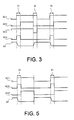
- the time sequence illustrated in Fig. 3 and described before, allows the control, through the control terminal TC, of the operation of the switch module 200, by imposing on it one or the other of the "on” and “off” states and, when necessary, one or the other of the first and second transitions.
- the driving device 500 described above ensures that, advantageously, during the "on” and “off” states, the control terminal TC is connected to the first and the second reference potentials V1 and V2, respectively, which, as already noticed, suitably have a high immunity level compared to disturbances related to the switching of the digital circuitry components of the processing system 100 itself.
- the first and second reference potentials V1 and V2 can coincide with the analog supply potentials VA1 and VA2, respectively, which are not affected by the influence of sudden digital switching operations of the processing system 100 digital circuitry, which is electrically connected to the digital supply potentials (VD1, VD2).
- the switch module 200 results to be insulated from the noise that is present on the digital supply potentials, during all the time intervals in which it is in the "on” state or the “off” state, that is, for a predominant part of its operation time. Accordingly, the switch module 200 performance will be appreciably improved, in terms of noise minimization and integrity preservation of the analog signal SA', the trend of which approaches to the ideal one, already described.
- the driving device 500 described above ensures that, in the time intervals associated to the transitions from the "on” state to the "off” state, and vice versa, the control terminal TC is instead electrically connected to the further third and fourth reference potentials V3 and V4, which are, as already known, electrically distinct from the analog supply potentials VA1, VA2.
- the third and fourth reference potentials V3, V4 coincide with the digital supply potentials VD1 and VD2, respectively, which are electrically distinct from the analog supply potentials VA1 and VA2, as required.
- the driving stage 520 allows conveniently affording the general case in which the switching currents associated both to the first and to the second transitions of the switch module 200 are "conveyed" on digital supply potentials, when the processing system 100 operation requires to avoid disturbances on both the analog supply potentials (VA1 and VA2).
- the driving device 500 of Fig. 2 is conveniently modified.
- a driving device 500' is now described, which can be used in the case in which the switching current associated to the second transition ("off/on") does not create disturbances and/or problems in the processing system 100, even when it flows through the analog supply terminal TA1, disturbing, during the transition itself, the relative analog supply potential VA1.
- the driving device 500' of Fig. 4 comprises a control module 510', a driving stage 520', and a switch module 200' (completely analogous to the switch module 200 of Fig. 2 ).
- the driving stage 520' results to be completely analogous to the driving stage 520, except for the fact that it results to be lacking in the third transistor TR3.
- the driving stage 520' comprises: a first transistor TR1', completely analogous to the first transistor TR1 employed in the driving stage 520; a second transistor TR2', completely analogous to the second transistor TR2 employed in the driving stage 520; a further transistor TR4', completely analogous to the fourth transistor TR4 employed in the driving stage 520.
- circuital connections of the respective drain (D1', D2', D4') and source (S1', S2', S4') terminals of the transistors (TR1', TR2', TR4') employed in the driving stage 520' are completely analogous to circuital connections of the drain (D1, D2, D4) and source (S1, S2, S4) terminals of the first (TR1), second (TR2), and fourth (TR4) transistors of the driving stage 520, respectively.
- control module 510' it is configured to generate a further plurality of driving control signals SCP' to be provided to the driving stage 520'.
- the further plurality of driving control signals SCP' comprises a first SC1', a second SC2', and a further SC4' driving control signals, which are provided to a first G1', second G2', further G4' gate terminals, respectively, with which the transistors TR1', TR2', TR4' are provided, respectively.
- the configuration of the driving stage 520' of Fig. 4 is such that, according to the switching on or switching off of the first transistor TR1', of the second transistor TR2', of the further transistor TR4', the control terminal TC', with which the switch module 200' is provided, can be operatively connected: to the first reference potential V1 (i.e., to the analog supply potential VA1) during the first state "on” and during the second transition "off/on” of the switch module 200'; to the second reference potential V2 (i.e., to the analog supply potential VA2) during the second state "off” of the switch module 200'; to the fourth reference potential V4 (i.e., to the digital supply potential VD2) during the first transition "on/off” of the switch module 200'.
- V1 i.e., to the analog supply potential VA1
- VA1 analog supply potential
- the switching off and on of the transistors TR1', TR2', TR4', according to the modes described above, occurs on the basis of the further plurality of driving control signals SCP' provided by the control module 510', according to the time evolution diagram illustrated in Fig. 5 .
- the driving stage 520' of Fig. 4 is satisfactory in the particular cases in which only the switch current associated to the first transition "on/off" creates disturbances and/or problems in the processing system 100, when it flows through the analog supply terminal TA2, perturbing, during the transition itself, the relative analog supply potential VA2.
- This situation can occur, for example, when the processing system 100 is an ADC converter in which analog samples voltage values of the analog signal SA' are stored after the switch module 200 (200') is "switched off” (that is, after the first transition "on/off"), referring the relative voltage measure to an analog ground potential (such as, for example, VA2).
- an analog ground potential such as, for example, VA2
- the fact of avoiding that the "analog ground” (that is, the potential VA2) is perturbed during the first transition "on/off” of the switch module 200 (200') advantageously allows minimizing distortions in the measurement of the stored voltage value.
- the embodiment of Fig. 4 meets the requirements, further resulting simpler, from a circuital point of view, compared to the embodiment of Fig. 2 .
- Such further embodiment comprises two transistors, for example, of the P-channel MOS type, the respective source terminals of which are connected to the analog supply potentials VA1 and to the digital supply potential VD1, respectively; and a further transistor, for example, of the N-channel MOS type, the source terminal of which is connected to the analog supply potential VA2.
- the driving control module (510, 510'), arranged to generate the plurality of driving control signals (SCP, SCP'), can be implemented through logical ports and/or components, according to various combinations and/or configurations, which are anyhow known to those of ordinary skill in the art.
- control module 510 after receiving a system control signal SCS1 (which is, for example, the signal commonly used in the prior art to generate the driving signal SP, for example, by an "inverter") from the digital control circuitry 600, generates, on the basis of this, the plurality of driving control signals SCP (SCP') ( Figs. 3 and 5 ).
- SCS1 which is, for example, the signal commonly used in the prior art to generate the driving signal SP, for example, by an "inverter”
- SCP' driving control signals SCP
- control module 510 (510'), accessible to those of ordinary skill in the art, can be for example provided for in the case in which the above-mentioned time values t1 and t2 are selected so as to have mutually different values (as in the example of Fig. 3 ).
- control module 510 (510') can be implemented through a network of logical ports (for example, OR, AND, NOR, NAND) to which analog and/or digital members are added to achieve the desired delays.
- logical ports for example, OR, AND, NOR, NAND
- switch module 200 preferably comprises only one analog signal pass transistor.
- the present invention applies also in the case in which the switch module comprises more "pass transistors", for example, a N-channel one and a P-channel one in parallel (for example, to operate on analog signals with higher amplitude ranges).
- a driving device could be suitably used, comprising more driving stages, bearing in mind the teachings of the present invention.
- the object of the present invention is fully achieved, since the processing system 100 can advantageously reduce in a remarkable way the noise associated to the driving of the switch module during the "on" and "off” states.
- the processing system of the invention further allows minimizing the disturbances on the entire analog circuitry of the processing system 100 during the switch module transitions from one to the other of its states.
- the processing system 100, and particularly the driving device 500 can therefore achieve a better performance compared to those that can be achieved by the known solutions.
Landscapes
- Electronic Switches (AREA)
- Analogue/Digital Conversion (AREA)
- Signal Processing Not Specific To The Method Of Recording And Reproducing (AREA)
- Control Of Indicators Other Than Cathode Ray Tubes (AREA)
Abstract
The control terminal of an analogue switch is driven by the analogue references when no transitions of the state of the switch are occurring in order to avoid switching noise of the digital circuitry to be transferred to the output of the switch, and by the digital references when transitions of the state of the switch are occurring in order to avoid distorsions on the analogue circuitry.
Description
- The present invention relates to (electronic and/or micro-electronic) systems for the processing of analog-type electrical signals by means of the use of an analog circuitry and a digital circuitry, and in particular to a processing system of analog electrical signal according to the preamble of
claim 1. - In a processing (electronic and/or micro-electronic) system of analog-type electrical signals (hereinafter, for brevity's sake simply being referred to as analog signals), a switch module (switch) is typically employed, in particular applications, which is capable of enabling and inhibiting the transfer of an analog signal from a source module to a user module.
- For example, in an Analog-to-Digital Converter system ADC, the switch module is employed, as it is known, for the sampling function, by storing the analog signal value while the switch module results to be in the so-called "off" state.
- In a Digital-to-Analog Converter system DAC, the switch module is also employed for the transfer of an analog signal towards an amplification stage, in predetermined time instants in which the same results to be in the so-called "on" state.
- An important requirement demanded to a switch module that is used in such systems is that of transferring the analog signal, on which it operates, in the most reliable way possible. In other words, it is required that the noise and/or the distortion added by the switch module to the transferred analog signal are reduced as much as possible (being ideally equal to zero).
- Typically, a switch module operating on analog signals is driven by a corresponding control digital circuitry, having the task to generate control logic signals of the switch module and to provide to it, through a driving device, a driving electrical signal, on the basis of the above-mentioned control logic signals, to allow the opening (state "off") or the closure (state "on") of the switch module.
- Such driving device has the drawback of further perturbing the analog signal on which the switch module operates, adding noise and/or distortion to it, even in a significant amount.
- This is due to the fact that such driving device takes the driving electrical signal from a supply circuitry internal to the electronic and/or micro-electronic system for the processing of analog electrical signals.
- In particular, as regards such supply circuitry, it is pointed out that such system usually comprises two different types of it: a so-called "analog supply" circuitry, to which the system analog circuitry is electrically connected; and a so-called "digital supply" circuitry, to which the system digital circuitry is electrically connected.
- As it is known, the "analog" supply is capable of providing, in a plurality of analog supply terminals, a first and a second analog supply potentials, while the "digital" supply is capable of providing, in a plurality of digital supply terminals, a first and a second digital supply potentials.
- Such first supply potentials (both analog and digital) can originate from, or coincide with, a first external supply potential, having a same nominal value one to the other. Similarly, such second supply potentials (both analog and digital) can originate from, or coincide with, a second external supply potential, having a same nominal value one to the other. Such first and second external supply potentials can be, for example, obtained from a battery.
- However, the "real" instantaneous values of such supply potentials can vary, departing from the nominal value. Particularly, the digital supply is usually characterized by a higher "switch noise", associated to the switching operations of the digital components connected thereto.
- The availability of two supply circuitries is a compromise that is usually adopted among the availability of an individual supply circuitry, that would lead to a degraded performance mainly due to excessive undesired mutual influences determined by the different operating modes of the digital components and the analog components, and the availability of a number of different supply circuitries, to which single subsystems of the system would refer, which would improve the performance by minimizing the mutual influences, but would lead to unacceptable costs and space waste.
- Typically, the switch module control circuitry is connected to the digital supply. In such scenario, also the corresponding driving device results to be connected to the digital supply, which constitutes the last control circuitry component before the switch module, and which directly interacts with the same switch module through said driving electrical signal.
- The driving device, connected to the digital supply, has the drawback that it transfers at least partially on the switch module, and therefore on the analog signal on which it operates, the switch noise that is present on the digital supply. Particularly, such noise is present both in the periods in which the switch module is "on" and in those in which it is "off".
- Therefore, the general need of employing a driving device that minimizes the noise transferred from it to the switch module is strongly felt.
- A known solution to cope with such drawback is the use of a driving device that is connected to the analog supply (which, as it is known, is already available) instead of being connected to the digital supply.
- Such solution exploits the advantage that the analog supply, as it is known, has a noticeably lower noise compared to the digital one, since the switch noise of the digital components, which are connected to the digital supply, is not present therein.
- However, such solution, while on one hand reducing the drawback due to the switch noise, has the disadvantage of introducing further distortions on the analog signal on which the switch module operates.
- This is due to the fact that the driving device switching currents, during the time intervals associated to the switch module transition from one to the other of the relative states ("on", "off"), result to be suddenly variable.
- In this scenario, such currents flow through the analog supply terminals, thus perturbing the already mentioned analog supply potential values.
- In fact, such switching currents create undesired voltages on the non-zero resistances of the internal supply paths. Furthermore, the perturbations induced by the switching currents on the analog supply, caused for example by stray phenomena, particularly related to the inductance, on the analog supply bondings, are particularly serious. In fact, besides distorting the analog signal on which the switch module operates, they affect the operation of the entire system analog circuitry, connected to such supply, thereby reducing the performance thereof.
- The object of the present invention is to devise and provide an improved system for the processing of analog electrical signals employing a driving device that allows to at least partially obviate the drawbacks described above with reference to the prior art.
- Such object is achieved by a system in accordance with
claim 1. - Further embodiments of such system are defined in the
dependent claims 2 to 12. - Further characteristics and advantages of the analog electrical signals processing system according to the invention will result from the description reported below of preferred embodiments, given by way of non-limiting example, with reference to the annexed Figures, in which:
-
Fig. 1 schematically shows an electronic system according to an example of the invention; -
Fig. 2 shows, from a circuit point of view, a driving device and a switch module that are employed in the electronic system ofFig. 1 ; -
Fig. 3 shows logic signals that are used for controlling the driving device ofFig. 2 , in a time evolution diagram; -
Fig. 4 illustrates, from a circuit point of view, a further driving device and a switch module that are used in an electronic system according to a further example of the invention; and -
Fig. 5 shows logic signals that are used for controlling the driving device ofFig. 4 , in a time evolution diagram. - With reference to
Fig. 1 , a processing system of analog electrical signals is now described, indicated on the whole by thereference numeral 100, according to an example of the present invention. - To the aims of the present description, by processing system of an analog electrical signals is meant an electronic and/or micro-electronic system, preferably manufactured by integrated technology (on "chip"), designed to carry out on such signals, by the use of an analog circuitry and a digital circuitry, one of more functions and/or operations, per se known to those of ordinary skill in the art, such as, for example, switching, signal transfer, analog-to-digital conversion, digital-to-analog conversion, and so on.
- It shall be noticed that the subsystems comprised in the processing system of analog electrical signals according to the invention, that will be described herein below, can be implemented without distinction in a single chip or by a plurality of chips. The processing system of analog electrical signals that will be described herein below is independent from the choice of the implementation partitioning of the various subsystems between one or more chips.
- The
processing system 100 comprises asource module 300 of an analog electrical signal SA, hereinafter also simply analog signal. - The
processing system 100 further comprises auser module 400, suitable to receive, on request, the analog signal SA generated by thesource module 300. - It is pointed out that the type of the
source module 300 and of theuser module 400 depends on the type of functions and/or operations that are carried out by theprocessing system 100. - The
processing system 100 further comprises aswitch module 200, per se known, operatively connected between thesource module 300 and theuser module 400. - Particularly, the
switch 200 comprises aninput terminal 201 arranged to receive in input the analog signal SA, and anoutput terminal 202, to provide the analog signal SA to theuser module 400, when required. - From an operative point of view, the
switch module 200 results to be so configured as to assume a first or a second states, in order to enable and inhibit, respectively, the transfer of the analog signal SA from thesource module 300 to theuser module 400, on the basis of a driving electrical signal SP (for brevity's sake hereinafter also referred to as driving signal), that will be described below. - It shall be noticed that in the first state (also referred to as "switched on", or "on"), the
switch module 200 behaves as a closed switch; in the second state (also referred to as "switched off", or "off"), theswitch module 200 behaves as an open switch. - Referring to
Fig. 1 , it shall be noticed that the analog signal that is present on theoutput terminal 202 is identified by the reference SA'. In the light of the mentioned operating mode of theswitch module 200, the analog signal SA' is ideally equal to the analog signal SA when theswitch module 200 assumes the first state, and it is equal to 0 (null signal) when theswitch module 200 assumes the second state. In practice, such analog signal SA' departs from the above-mentioned ideal trend, because of the noise or of other disturbance types. - The
processing system 100 further comprises adriving device 500 of theswitch module 200. In more detail, thedriving device 500 results to be so configured as to drive, on the basis of the driving signal SP, a control terminal TC which theswitch module 200 is provided with, so as to allow it to assume the first or the second state and to carry out a first driving transition type (hereinafter for brevity's sake also referred to as "first driving transition") from the first state to the second state, and a second driving transition type (hereinafter for brevity's sake also referred to as "second driving transition") from the second state to the first state. - It is pointed out that the first and the second transition types are intrinsically associated to the dynamic operation of the
switch module 200. Particularly, as it is known, each specific occurrence of one of such driving transitions occurs in a time interval that is associated to the above-mentioned transition, within which the transition itself takes place. Such time interval usually has a short duration compared to the duration of the successive "on" or "off" state of theswitch module 200. In other words, the time interval associated to a driving transition can also be regarded as a "fraction" of the "on" state or the "off" state of theswitch module 200. - Referring back to the
driving device 500 ofFig. 1 , it further comprises adriving device 500 control module 510 (hereinafter, for brevity's sake, control module), so configured as to generate a plurality of driving control signals SCP, which will be described herein below, on the basis of one or more system control signals SCS. - The
driving device 500 further comprises a drivingstage 520 operatively interposed between thecontrol module 510 and theswitch module 200. - In more detail, the driving
stage 520 results to be configured to receive the plurality of control signals SCP from thecontrol module 510 and to generate, on the basis of said plurality, the driving signal SP. - The driving
stage 520 will be described in more detail herein below, in some embodiments thereof, with particular reference toFigs. 2 and4 . - Referring again to
Fig. 1 , theprocessing system 100 further comprises a system controldigital circuitry 600, arranged to generate, inter alia, one or more system control signals SCS intended to control, through thecontrol module 510, the drivingstage 520, and to accordingly determine the operation of theswitch module 200. The system controldigital circuitry 600, per se known, comprises, for example, a plurality of logical ports and/or components, and can vary depending on the type of theprocessing system 100 for which it is designed. - The
processing system 100 further comprises a first reference terminal T1 and a second reference terminal T2 associated, respectively, to a first reference potential V1 and a second reference potential V2. - Such reference potentials (V1, V2) advantageously have a high immunity level compared to disturbances related to the switching of the digital circuitry components with which the
processing system 100 is provided. - The
processing system 100 further comprises a third reference terminal T3 and a fourth reference terminal T4 associated, respectively, to a third reference potential V3 and a fourth reference potential V4. - It is pointed out that the third and fourth reference potentials (V3, V4) are advantageously chosen so as to result to be electrically distinct, respectively, from the first and the second reference potentials (V1, V2).
- The
processing system 100 further comprises an analogcircuitry supply circuitry 10, arranged to provide a first and a second analog supply potentials (VA1, VA2), for example, on corresponding analog supply terminals (TA1, TA2). - Referring to
Fig. 1 , it shall be noticed that thesource module 300 and theuser module 400 are operatively connected, in order to be supplied, to the analog supply terminals TA1, TA2. It has to be further noticed that, usually, other analog circuitry components, with which theprocessing system 100 can be provided (not shown in the Figure), whether they are integrated or not in the same chip of theanalog supply circuitry 10 and/or of theother processing system 100 subsystems, can be operatively connected to the analog supply terminals TA1, TA2. - It shall be further noticed that, in the embodiment of the
processing system 100 ofFig. 1 , the first and the second reference terminals T1, T2 respectively coincide with the analog supply terminals TA1, TA2. Similarly, the first and the second reference potentials V1, V2 respectively coincide with the analog supply potentials VA1, VA2. - In fact, the analog supply potentials VA1 and VA2 usually have, as required for the reference potentials V1 and V2, a high immunity level compared to the disturbances related to the switching of the
processing system 100 digital circuitry components. - The
processing system 100 further comprises a digitalcircuitry supply circuitry 20, arranged to provide a first digital supply potential VD1 and a second digital supply potential VD2, for example, on respective digital supply terminals TD1, TD2. It shall be further noticed that other digital circuitry components which theprocessing system 100 can be provided with (not shown in the Figure), whether they are integrated or not in the same chip of thedigital supply circuitry 20 and/or of theother processing system 100 subsystems, can be usually operatively connected to the analog supply terminals TD1, TD2. - Referring to
Fig. 1 , it has to be observed that, for example, thedigital control circuitry 600 and thecontrol module 510 are operatively connected, in order to be supplied, to the terminals TD1 and TD2. - Referring again to the analog
circuitry supply circuitry 10 and to the digitalcircuitry supply circuitry 20, it has to be observed that, according to different embodiments of the present invention, they can be integrated in the same chip that houses the circuitries which they supply, or they can be in one or more different chips. - Referring back to the embodiment of
Fig. 1 , it shall be noticed that the third and the fourth reference terminals T3, T4 respectively coincide with the digital supply terminals TD1, TD2. - Similarly, the third and the fourth reference potentials V3, V4 respectively coincide with the digital supply potentials VD1, VD2.
- In fact, the digital supply potentials VD1, VD2, as required for the reference potentials V3, V4, usually result to be electrically distinct from the first and the second reference potentials (V1, V2), respectively.
- It has to be observed that, as it is known, the analog supply potential (VA1, VA2) nominal values are usually equal to the digital supply potentials (VD1, VD2) nominal values, respectively, while the corresponding real and instantaneous values can differ from one another, since each of them can vary in time, because of several non-idealities (for example, noise).
- Referring again to the example of
Fig. 1 , the drivingstage 520 results to be operatively connected both to the pair composed of the first and the second reference terminals (T1, T2) and to the pair composed of the third and the fourth reference terminals (T3, T4) . - With particular reference to
Fig. 2 , the drivingstage 520 is now described, according to an embodiment example. It is pointed out that, for clarity of description, thecontrol module 510, operatively connected to the drivingstage 520, as already illustrated before, to provide it with the plurality of driving control signals SCP, and theswitch module 200 driven by the drivingstage 520 through the control terminal TC, already introduced before, are schematically illustrated inFig. 2 . - The driving
stage 520 comprises a first transistor TR1, for example, of the P-channel MOS type, provided with: a first source terminal S1 electrically connected to the first reference potential V1, i.e., to the analog supply potential VA1; a first gate terminal G1 operatively connected to thecontrol module 510 to receive in input a first control signal SC1 belonging to the plurality of driving control signals SCP; a first drain terminal D1, operatively connected to the control terminal TC of theswitch module 200. - The driving
stage 520 further comprises a second transistor TR2, for example, of the N-channel MOS type, provided with: a second drain terminal D2 connected to the first drain terminal D1 of the first transistor TR1, and, consequently, to the control terminal TC of theswitch module 200; a second gate terminal G2 operatively connected to thecontrol module 510 to receive in input a second control signal SC2 belonging to the plurality of driving control signals SCP; a second source terminal S2, electrically connected to the second reference potential V2, i.e., to the analog supply potential VA2. - The driving
stage 520 further comprises a third transistor TR3, for example, of the P-channel MOS type, provided with: a third source terminal S3 electrically connected to the third reference potential V3, i.e., to the digital supply potential VD1; a third gate terminal G3 operatively connected to thecontrol module 510 to receive in input a third control signal SC3 belonging to the plurality of driving control signals SCP; a third drain terminal D3, also being operatively connected to the control terminal TC of theswitch module 200, as well as to the first drain terminal D1 of the first transistor TR1 and to the second drain terminal D2 of the second transistor TR2. - The driving
stage 520 further comprises a fourth transistor TR4, for example, of the N-channel MOS type, provided with: a fourth drain terminal D4 also operatively connected to the control terminal TC of theswitch module 200, as well as to the third drain terminal D3 of the third transistor TR3, to the first drain terminal D1 of the first transistor TR1 and to the second drain terminal D2 of the second transistor TR2; a fourth gate terminal G4 operatively connected to thecontrol module 510 to receive in input a fourth control signal SC4 belonging to the plurality of driving control signals SCP; a fourth source terminal S4 electrically connected to the fourth reference potential V4, i.e., to the digital supply potential VD2. - It shall be noticed that the driving
stage 520 configuration (Fig. 2 ) is such that, according to the switching on or off of the first transistor TR1, the second transistor TR2, the third transistor TR3, and the fourth transistor TR4, on the basis of the plurality of driving control signals SCP provided by thecontrol module 510, the control terminal TC can be operatively connected to the first reference potential V1 (i.e., to the analog supply potential VA1), the second reference potential V2 (i.e., the analog supply potential VA2), the third reference potential V3 (i.e., the digital supply potential VD1), or the fourth reference potential V4 (i.e., the digital supply potential VD2). - With particular reference to
Figs. 2 and3 , the operation of thedriving device 500 is now described according to the example ofFig. 2 . - It is assumed that the first state ("on") is initially imposed to the
switch module 200. - The
control module 510 is configured so that the third control signal SC3 is at a high logical level ("1"). It results that the third transistor TR3 is in the "switched off" condition and it behaves as an "open switch" between the respective source S3 and drain D3 terminals. - The
control module 510 is further configured so that the fourth control signal SC4 is at a low logical level ("0"). This implies that the fourth transistor TR4 is in the "switched off" condition and acts as an "open switch" between the respective source S4 and drain D4 terminals. - Furthermore, the
control module 510 is configured so that the second control signal SC2 is at a low logical level ("0"). This implies the switching off of the second transistor TR2, which behaves as an "open switch", between the respective source S2 and drain D2 terminals. - Finally, the
control module 510 is configured so that the first control signal SC1 is at a low logical level ("0"). This implies that the first transistor TR1 is in the "switch on" condition and allows the electric connection between the respective source S1 and drain D1 terminals. Accordingly, the control terminal TC of theswitch module 200, operatively connected to the first drain terminal D1, is electrically connected also to the first source terminal S1, therefore resulting to be electrically connected to the first reference potential V1, i.e., to the analog supply potential VA1. The first reference potential V1 has such a value as to correspond to a "high" logical level ("1"). Therefore, in the described configuration, also the driving signal SP, which is present at the control terminal TC of theswitch module 200, results to be corresponding to a "high" logical level, with which it imposes the first state ("on") of theswitch module 200. - With particular reference to the time diagram of
Fig. 3 , it shall be noticed that, each time that it is desired that theswitch module 200 carries out the first transition (from the first state "on" to the second state "off"), thecontrol module 510 results to be configured so that the third control signal SC3 is maintained to a high logical level ("1"); the second control signal SC2 is maintained to a low logical level ("0"); the first control signal SC1 is brought to a high logical level ("1"), in which the first transistor TR1 electrically disconnects the first drain terminal D1, and accordingly the control terminal TC, from the first source terminal S1, and therefore from the first reference potential V1; the fourth control signal SC4 is brought to a high logical level ("1"), in which the fourth transistor TR4 electrically connects the fourth drain terminal D4, and accordingly the control terminal TC, to the fourth source terminal S4, and therefore to the fourth reference potential V4, i.e., to the digital supply potential VD2. - In such configuration, the transistor TR1 behaves as an "open switch", while the transistor TR4 behaves as a "closed switch".
- Furthermore, the fourth reference potential V4 has such a value as to correspond to a "low" logical level ("0"). Therefore, the driving signal SP present at the control terminal TC passes, during the first transition, from a "high" logical level to a "low" logical level, with which it imposes the corresponding transition from the first state "on" to the second state "off" to the
switch module 200. - This advantageously allows to make the switching current, associated to the above-mentioned transition of the driving signal SP, to flow through the digital supply terminal TD2 associated to the fourth reference potential V4, i.e., to the digital supply potential VD2.
- Referring again to
Figs. 2 and3 , it is now assumed the case in which the second state ("off") is imposed to theswitch module 200. - The
control module 510 is configured so that the third control signal SC3 is maintained to a high logical level ("1"); the first control signal SC1 is maintained to a high logical level ("1"). Furthermore, thecontrol module 510 is configured so that the fourth control signal SC4 is brought to a "low" logical level ("0"), in which the fourth transistor TR4 electrically disconnects the fourth drain terminal D4, and accordingly the control terminal TC, from the fourth source terminal S4, and therefore from the fourth reference potential V4, i.e., from the digital supply potential VD2. Finally, thecontrol module 510 is configured so that the second control signal SC2 is brought to a "high" logical level ("1") in which the second transistor TR2 electrically connects the second drain terminal D2, and accordingly the control terminal TC, to the second source terminal S2, and therefore to the second reference potential V2, i.e., to the analog supply potential VA2. - In such configuration, the fourth transistor TR4 behaves as an "open switch", while the second transistor TR2 behaves as a "closed switch".
- Furthermore, the second reference potential V2 has such a value as to correspond to a "low" logical level ("0"). Therefore, in the described configuration, also the driving signal SP present at the control terminal TC of the
switch module 200 results to be corresponding to a "low" logical level, with which it imposes the second state ("off") of theswitch module 200. - With particular reference to the time diagram of
Fig. 3 , it shall be noticed that each time that it is desired that theswitch module 200 carries out the second transition (from the second state "off" to the first state "on"), thecontrol module 510 is configured so that the first control signal SC1 is maintained at a high logical level ("1"); the fourth control signal SC4 is maintained at a low logical level ("0"); the second control signal SC2 is brought to a low logical level ("0"), in which the second transistor TR2 electrically disconnects the second drain terminal D2, and accordingly the control terminal TC, from the second source terminal S2, and therefore from the second reference potential V2, i.e., from the analog supply potential VA2; the third control signal SC3 is brought to a low logical level ("0"), in which the third transistor TR3 electrically connects the third drain terminal D3, and accordingly the control terminal TC, to the third source terminal S3, and therefore to the third reference potential V3, i.e., to the digital supply potential VD1. - In such configuration, the transistor TR2 behaves as an "open switch", while the transistor TR3 behaves as a "closed switch".
- Furthermore, the third reference potential V3 has such a value as to correspond to a "high" logical level ("1"). Therefore, the driving signal SP present at the control terminal TC passes, during said second transition, from a "low" logical level to a "high" logical level, with which it imposes to the
switch module 200 the corresponding transition from the second state "off" to the first state "on". - This advantageously allows to make the switching current, associated to the above-mentioned transition of the driving signal SP, to flow through the digital supply terminal TD1 associated to the third reference potential V3, i.e., to the digital supply potential VD1.
- The time sequence described above restarts then from a period in which the
switch module 200 is maintained in its first state "on", since at the end of the time interval associated to the second "off/on" transition, thecontrol module 510 is configured to bring the third control signal SC3 to a "high" logical level, and the first control signal SC1 to a "low" logical level, returning, actually, to the situation already described with reference to the first state "on" of theswitch module 200. - With particular reference now to
Fig. 3 only, it shall be noticed that each of the time intervals associated to the first driving transition has a duration t1 and each of the time intervals associated to the second driving transition has a duration t2. Usually, the durations t1, t2 of such time intervals results to be much shorter compared to the duration of the time intervals in which theswitch module 200 is maintained in the first state "on" or the second state "off". The duration values t1 and t2 are usually similar, and can also be equal one to the other. - From an operative point of view, the time sequence, illustrated in
Fig. 3 and described before, allows the control, through the control terminal TC, of the operation of theswitch module 200, by imposing on it one or the other of the "on" and "off" states and, when necessary, one or the other of the first and second transitions. - Furthermore, the driving
device 500 described above ensures that, advantageously, during the "on" and "off" states, the control terminal TC is connected to the first and the second reference potentials V1 and V2, respectively, which, as already noticed, suitably have a high immunity level compared to disturbances related to the switching of the digital circuitry components of theprocessing system 100 itself. Particularly, as in the example shown (Fig. 2 ), the first and second reference potentials V1 and V2 can coincide with the analog supply potentials VA1 and VA2, respectively, which are not affected by the influence of sudden digital switching operations of theprocessing system 100 digital circuitry, which is electrically connected to the digital supply potentials (VD1, VD2). - This advantageously implies that the
switch module 200 results to be insulated from the noise that is present on the digital supply potentials, during all the time intervals in which it is in the "on" state or the "off" state, that is, for a predominant part of its operation time. Accordingly, theswitch module 200 performance will be appreciably improved, in terms of noise minimization and integrity preservation of the analog signal SA', the trend of which approaches to the ideal one, already described. - Going even further, the driving
device 500 described above ensures that, in the time intervals associated to the transitions from the "on" state to the "off" state, and vice versa, the control terminal TC is instead electrically connected to the further third and fourth reference potentials V3 and V4, which are, as already known, electrically distinct from the analog supply potentials VA1, VA2. - This very advantageously allows electrically insulating the analog supply potentials VA1, VA2 from the switching currents, which are relatively ample and suddenly variable, associated to the transition of the driving signal SP from a "high" logical level to a "low" one, or vice versa, during the respective first and second transitions of the
switch module 200. - Therefore, the disturbances introduced on the analog supply potentials VA1, VA2 results to be drastically reduced, (ideally reduced to zero), and the performance degradations of a part or even of the entire analog circuitry of the
processing system 100 results to be minimized accordingly, degradations which could be unacceptable for the operation of theprocessing system 100 itself. - Inter alia, it shall be noticed that, advantageously, also the distortions introduced on the analog signals SA, SA' through the
source module 300 and theuser module 400 are minimized. - It shall be noticed that, in the embodiment of the
processing system 100 ofFig. 2 , the third and fourth reference potentials V3, V4 coincide with the digital supply potentials VD1 and VD2, respectively, which are electrically distinct from the analog supply potentials VA1 and VA2, as required. - This satisfies the need of adopting the proposed solution in a processing system, usually comprising two supply circuitries (the "analog" and the "digital" one), avoiding the addition of further supply circuitries, that would be problematic in terms of cost and occupied space.
- Finally, it shall be noticed that, despite the fact that in the intervals in which the driving signal SP is connected to the digital supply potentials VD1, VD2 a relatively high noise (related to the digital supply) is present, this does not create relevant problems. In fact, the time intervals associated to the above-mentioned transitions are usually very short compared to the time intervals associated to the "on" and "off" states.
- In the embodiment illustrated in
Fig. 2 , the drivingstage 520 allows conveniently affording the general case in which the switching currents associated both to the first and to the second transitions of theswitch module 200 are "conveyed" on digital supply potentials, when theprocessing system 100 operation requires to avoid disturbances on both the analog supply potentials (VA1 and VA2). - However, there are cases in which the disturbances to be obviated originate from the switching current associated to only one of the two transitions ("on/off", "off/on").
- To this aim, the driving
device 500 ofFig. 2 is conveniently modified. - By way of example, with reference to
Fig. 4 , a driving device 500' is now described, which can be used in the case in which the switching current associated to the second transition ("off/on") does not create disturbances and/or problems in theprocessing system 100, even when it flows through the analog supply terminal TA1, disturbing, during the transition itself, the relative analog supply potential VA1. - The driving device 500' of
Fig. 4 comprises a control module 510', a driving stage 520', and a switch module 200' (completely analogous to theswitch module 200 ofFig. 2 ). - From a circuital point of view, the driving stage 520' results to be completely analogous to the driving
stage 520, except for the fact that it results to be lacking in the third transistor TR3. - Particularly, the driving stage 520' comprises: a first transistor TR1', completely analogous to the first transistor TR1 employed in the driving
stage 520; a second transistor TR2', completely analogous to the second transistor TR2 employed in the drivingstage 520; a further transistor TR4', completely analogous to the fourth transistor TR4 employed in the drivingstage 520. - The circuital connections of the respective drain (D1', D2', D4') and source (S1', S2', S4') terminals of the transistors (TR1', TR2', TR4') employed in the driving stage 520' are completely analogous to circuital connections of the drain (D1, D2, D4) and source (S1, S2, S4) terminals of the first (TR1), second (TR2), and fourth (TR4) transistors of the driving
stage 520, respectively. - As regards the control module 510', it is configured to generate a further plurality of driving control signals SCP' to be provided to the driving stage 520'.
- Particularly, the further plurality of driving control signals SCP' comprises a first SC1', a second SC2', and a further SC4' driving control signals, which are provided to a first G1', second G2', further G4' gate terminals, respectively, with which the transistors TR1', TR2', TR4' are provided, respectively.
- Referring to
Figs. 4 and5 , the operation of the driving stage 520' is now described. - It shall be noticed that the configuration of the driving stage 520' of
Fig. 4 is such that, according to the switching on or switching off of the first transistor TR1', of the second transistor TR2', of the further transistor TR4', the control terminal TC', with which the switch module 200' is provided, can be operatively connected: to the first reference potential V1 (i.e., to the analog supply potential VA1) during the first state "on" and during the second transition "off/on" of the switch module 200'; to the second reference potential V2 (i.e., to the analog supply potential VA2) during the second state "off" of the switch module 200'; to the fourth reference potential V4 (i.e., to the digital supply potential VD2) during the first transition "on/off" of the switch module 200'. - The switching off and on of the transistors TR1', TR2', TR4', according to the modes described above, occurs on the basis of the further plurality of driving control signals SCP' provided by the control module 510', according to the time evolution diagram illustrated in
Fig. 5 . - The driving stage 520' of
Fig. 4 is satisfactory in the particular cases in which only the switch current associated to the first transition "on/off" creates disturbances and/or problems in theprocessing system 100, when it flows through the analog supply terminal TA2, perturbing, during the transition itself, the relative analog supply potential VA2. - This situation can occur, for example, when the
processing system 100 is an ADC converter in which analog samples voltage values of the analog signal SA' are stored after the switch module 200 (200') is "switched off" (that is, after the first transition "on/off"), referring the relative voltage measure to an analog ground potential (such as, for example, VA2). In this case, the fact of avoiding that the "analog ground" (that is, the potential VA2) is perturbed during the first transition "on/off" of the switch module 200 (200'), advantageously allows minimizing distortions in the measurement of the stored voltage value. On the other hand, in this particular case, there are not strict requirements about the second transition "off/on" of the switch module 200 (200'). - Therefore, in a case as the one described above, the embodiment of
Fig. 4 meets the requirements, further resulting simpler, from a circuital point of view, compared to the embodiment ofFig. 2 . - Completely similarly, the further "dual" embodiment of the one in
Fig. 4 can be understood, which is not illustrated, as being easily inferable by those of ordinary skill in the art, in light of the embodiments inFigs. 2 and4 . - Such further embodiment comprises two transistors, for example, of the P-channel MOS type, the respective source terminals of which are connected to the analog supply potentials VA1 and to the digital supply potential VD1, respectively; and a further transistor, for example, of the N-channel MOS type, the source terminal of which is connected to the analog supply potential VA2.
- The operation of such embodiment can be easily inferred by those of ordinary skill in the art, mutatis mutandis, by observing the embodiment in
Figs. 2 and4 . - Referring to the different embodiments hereto described, the driving control module (510, 510'), arranged to generate the plurality of driving control signals (SCP, SCP'), can be implemented through logical ports and/or components, according to various combinations and/or configurations, which are anyhow known to those of ordinary skill in the art.
- For example, it is considered the case in which the
control module 510, after receiving a system control signal SCS1 (which is, for example, the signal commonly used in the prior art to generate the driving signal SP, for example, by an "inverter") from thedigital control circuitry 600, generates, on the basis of this, the plurality of driving control signals SCP (SCP') (Figs. 3 and 5 ). Those of ordinary skill in the art, by examining the time evolution diagrams inFig. 3 and 5 , can easily find that the control signals can be generated starting from the system control signal SCS1, through the generation of a further auxiliary signal (which is, for example, the logical inverse of the system control signal SCS1, delayed by a time value t1, in the case ofFig. 5 in which t1 is equal to t2) and through a suitable combination, through logical operations, of the system control signal SCS1 and the further auxiliary signal. - Optional modifications of the control module 510 (510'), accessible to those of ordinary skill in the art, can be for example provided for in the case in which the above-mentioned time values t1 and t2 are selected so as to have mutually different values (as in the example of
Fig. 3 ). - Therefore, to such purposes, the control module 510 (510') can be implemented through a network of logical ports (for example, OR, AND, NOR, NAND) to which analog and/or digital members are added to achieve the desired delays.
- As regards the
switch module 200, it shall be noticed that in the described examples it preferably comprises only one analog signal pass transistor. - However, the present invention applies also in the case in which the switch module comprises more "pass transistors", for example, a N-channel one and a P-channel one in parallel (for example, to operate on analog signals with higher amplitude ranges). In such case, to drive the thus-configured switch module, a driving device could be suitably used, comprising more driving stages, bearing in mind the teachings of the present invention.
- As it can be observed, the object of the present invention is fully achieved, since the
processing system 100 can advantageously reduce in a remarkable way the noise associated to the driving of the switch module during the "on" and "off" states. At the same time, the processing system of the invention further allows minimizing the disturbances on the entire analog circuitry of theprocessing system 100 during the switch module transitions from one to the other of its states. In these aspects, theprocessing system 100, and particularly thedriving device 500, can therefore achieve a better performance compared to those that can be achieved by the known solutions. - To the embodiments of the processing system described above, those of ordinary skill in the art, in order to meet contingent needs, will be able to make modifications, adaptations, and replacements of elements with functionally equivalent other ones, without departing from the scope of the following claims. Each of the characteristics described as belonging to a possible embodiment can be implemented independently from the other embodiments described.
Claims (12)
- A processing system (100) of analog electrical signals by means of the use of an analog circuitry and a digital circuitry, comprising:- an analog circuitry supply circuitry (10) arranged to provide a first (VA1) and a second (VA2) analog supply potentials;- a switch module (200; 200') configured to assume a first state or a second state, in order to enable and inhibit, respectively, the transfer of an analog electrical signal (SA, SA') from a source module (300) to a user module (400), on the basis of a driving electrical signal (SP);- a driving device (500; 500') configured to drive, on the basis of the driving electrical signal (SP), a control terminal (TC; TC') of the switch module (200; 200'), so as to allow the switch module (200; 200') to assume the first or the second state, the driving device (500; 500') further allowing the switch module (200; 200') to carry out a first driving transition from the first state to the second state and a second driving transition from the second state to the first state;said driving device (500; 500') being configured to alternately connect the control terminal (TC; TC') to a first terminal (T1) connected to a first reference potential (V1) during the first state and to a second terminal (T2) connected to a second reference potential (V2) during the second state;
characterized in that the driving device (500; 500') results to be so configured as to connect the control terminal (TC; TC') of the switch module (200; 200') to at least one further terminal (T3, T4) connected to a third reference potential (V3, V4) electrically distinct from the first (VA1) and from the second (VA2) analog supply potentials, during each of the time intervals associated to at least one of said first and second driving transitions of the switch module (200; 200'). - The processing system (100) according to claim 1, wherein the driving device (500; 500') results to be so configured as to connect the control terminal (TC) of the switch module (200) to a fourth terminal (T4) connected to a fourth reference potential (V4), electrically distinct from the first (VA1) and from the second (VA2) analog supply potentials, the control terminal (TC) being connected to the at least one further terminal (T3, T4) and to the fourth terminal (T4) during each of the time intervals associated to the first and to the second transition of the switch module 200, respectively.
- The processing system (100) according to claim 1 or 2, wherein the first reference potential (V1) and the second reference potential (V2) coincide with the first analog supply potential (VA1) and the second analog supply potential (VA2), respectively.
- The processing system (100) according to one of the preceding claims, further comprising a digital circuitry supply circuitry (20) arranged to provide a first (VD1) and a second (VD2) digital supply potentials.
- The system according to claim 4, wherein the third reference potential (V3) and the fourth reference potential (V4) coincide with the first digital supply potential (VD1) and the second digital supply potential (VD2), respectively.
- The processing system (100) according to one of the preceding claims, wherein the driving device (500; 500') comprises a driving stage (520; 520'), said driving device (500; 500') further comprising a control module (510; 510') of the driving device (500; 500').
- The processing system (100) according to claim 6, further comprising a control digital circuitry (600) configured to provide one or more system control signals (SCS) to the driving device (500; 500'), said control module (510; 510') being so configured as to generate a plurality of driving control signals (SCP; SCP'), on the basis of said one or more system control signals (SCS).
- The processing system (100) according to claim 7, wherein said driving stage (520; 520) results to be so configured as to generate the driving electrical signal (SP) on the basis of the plurality of driving control signals (SCP; SCP').
- The processing system (100) according to one of the preceding claims, wherein the driving stage (520; 520') comprises a first transistor (TR1; TR1') having a first source terminal (S1; S1') electrically connected to the first reference potential (V1); a first gate terminal (G1; G1') operatively connected to the control module (510; 510') to receive a first control signal (SC1; SC1') of the plurality of driving control signals (SCP; SCP'); a first drain terminal (D1; D1'), operatively connected to the control terminal (TC) of the switch module 200.
- The processing system (100) according to claim 9, wherein the driving stage (520; 520') further comprises a second transistor (TR2; TR2') having a second drain terminal (D2; D2') connected to the first drain terminal (D1; D1') of the first transistor (TR1; TR1'); a second gate terminal (G2; G2') operatively connected to the control module (510; 510') to receive a second control signal (SC2; SC2') of the plurality of driving control signals (SCP; SCP'); a second source terminal (S2; S2'), operatively connected to the second reference potential (V2).
- The processing system (100) according to claim 10, wherein the driving stage (520; 520') further comprises a further transistor (TR4; TR4') having a further drain terminal (D4; D4') connected to the first drain terminal (D1; D1') of the first transistor (TR1; TR1'); a further gate terminal (G4; G4') operatively connected to the control module (510; 510') to receive a further control signal (SC4; SC4') of the plurality of driving control signals (SCP; SCP'); a further source terminal (S4; S4'), operatively connected to the fourth reference potential (V4).
- The processing system (100) according to claim 11, wherein the driving stage (520; 520') further comprises a further transistor (TR3; TR3') having a further source terminal (S3; S3') connected to the third reference potential (V3); a further gate terminal (G3; G3') operatively connected to the control module (510; 510') to receive a further control signal (SC3; SC3') of the plurality of driving control signals (SCP; SCP'); a further drain terminal (D3; D3'), operatively connected to the first drain terminal (D1; D1') of the first transistor (TR1; TR1').
Applications Claiming Priority (1)
| Application Number | Priority Date | Filing Date | Title |
|---|---|---|---|
| ITMI2009A001683A IT1395939B1 (en) | 2009-09-30 | 2009-09-30 | ANALOG-TYPE ELECTRICAL SIGNAL PROCESSING SYSTEM WITH LOW NOISE PILOT DEVICE |
Publications (1)
| Publication Number | Publication Date |
|---|---|
| EP2312632A1 true EP2312632A1 (en) | 2011-04-20 |
Family
ID=42139170
Family Applications (1)
| Application Number | Title | Priority Date | Filing Date |
|---|---|---|---|
| EP20100176594 Withdrawn EP2312632A1 (en) | 2009-09-30 | 2010-09-14 | System for processing analog-type electrical signals with low noise driving device |
Country Status (3)
| Country | Link |
|---|---|
| US (1) | US8427196B2 (en) |
| EP (1) | EP2312632A1 (en) |
| IT (1) | IT1395939B1 (en) |
Families Citing this family (1)
| Publication number | Priority date | Publication date | Assignee | Title |
|---|---|---|---|---|
| TWI764813B (en) * | 2021-08-18 | 2022-05-11 | 立積電子股份有限公司 | Driving circuit |
Citations (2)
| Publication number | Priority date | Publication date | Assignee | Title |
|---|---|---|---|---|
| JP2004297165A (en) * | 2003-03-25 | 2004-10-21 | Toshiba Corp | Analog / digital conversion circuit and communication device |
| US20080043540A1 (en) * | 2006-08-15 | 2008-02-21 | Boemler Christian M | Multilevel driver |
Family Cites Families (2)
| Publication number | Priority date | Publication date | Assignee | Title |
|---|---|---|---|---|
| US8143934B1 (en) * | 2008-07-01 | 2012-03-27 | Cypress Semiconductor Corporation | Analog switching system for low cross-talk |
| US8310301B2 (en) * | 2010-02-25 | 2012-11-13 | Fairchild Semiconductor Corporation | Fully featured control pin powered analog switch |
-
2009
- 2009-09-30 IT ITMI2009A001683A patent/IT1395939B1/en active
-
2010
- 2010-09-14 EP EP20100176594 patent/EP2312632A1/en not_active Withdrawn
- 2010-09-29 US US12/893,848 patent/US8427196B2/en not_active Expired - Fee Related
Patent Citations (2)
| Publication number | Priority date | Publication date | Assignee | Title |
|---|---|---|---|---|
| JP2004297165A (en) * | 2003-03-25 | 2004-10-21 | Toshiba Corp | Analog / digital conversion circuit and communication device |
| US20080043540A1 (en) * | 2006-08-15 | 2008-02-21 | Boemler Christian M | Multilevel driver |
Also Published As
| Publication number | Publication date |
|---|---|
| US8427196B2 (en) | 2013-04-23 |
| IT1395939B1 (en) | 2012-11-02 |
| ITMI20091683A1 (en) | 2011-04-01 |
| US20110095610A1 (en) | 2011-04-28 |
Similar Documents
| Publication | Publication Date | Title |
|---|---|---|
| KR100590464B1 (en) | Sampling switch | |
| US7408330B2 (en) | Voltage up-conversion circuit using low voltage transistors | |
| US7723867B2 (en) | Power gating of circuits | |
| US20130113524A1 (en) | Flexible low power slew-rate controlled output buffer | |
| US8415985B2 (en) | Circuits and methods for sampling and holding differential input signals | |
| CN101292426A (en) | Current addition type DAC | |
| US6501064B2 (en) | Image sensor with active sensor elements | |
| US20060114033A1 (en) | Sample -hold circuit | |
| US6590516B2 (en) | Current steering type D/A converter | |
| US8076966B2 (en) | Analog switch circuit for wide frequency band | |
| WO2004112247A1 (en) | Logic circuit having suppressed leak current to differential circuit | |
| US20200044639A1 (en) | Latch circuit | |
| US6326803B1 (en) | Terminating circuit for a transmission line | |
| US8970285B2 (en) | Dual supply level shifter circuits | |
| JP2001111407A (en) | Integrated semiconductor circuit | |
| US9240785B2 (en) | Analog signal compatible CMOS switch as an integrated peripheral to a standard microcontroller | |
| US8427196B2 (en) | System for processing analog-type electrical signals with low noise driving device | |
| US20110084755A1 (en) | Analog switch | |
| US7403046B2 (en) | Sample-and-hold circuits | |
| US8604863B2 (en) | Switch control circuit, semiconductor device, and radio communication device | |
| US8866466B2 (en) | Power generating circuit and switching circuit | |
| US6578185B1 (en) | Power-supply-configurable outputs | |
| US6175256B1 (en) | Control circuit | |
| US7298403B2 (en) | Image reading device | |
| CN223744706U (en) | Cascade circuit |
Legal Events
| Date | Code | Title | Description |
|---|---|---|---|
| PUAI | Public reference made under article 153(3) epc to a published international application that has entered the european phase |
Free format text: ORIGINAL CODE: 0009012 |
|
| AK | Designated contracting states |
Kind code of ref document: A1 Designated state(s): AL AT BE BG CH CY CZ DE DK EE ES FI FR GB GR HR HU IE IS IT LI LT LU LV MC MK MT NL NO PL PT RO SE SI SK SM TR |
|
| AX | Request for extension of the european patent |
Extension state: BA ME RS |
|
| STAA | Information on the status of an ep patent application or granted ep patent |
Free format text: STATUS: THE APPLICATION IS DEEMED TO BE WITHDRAWN |
|
| 18D | Application deemed to be withdrawn |
Effective date: 20111021 |