EP2310551B1 - Method of forming a tantalum-containing layer on a substrate - Google Patents
Method of forming a tantalum-containing layer on a substrate Download PDFInfo
- Publication number
- EP2310551B1 EP2310551B1 EP09780636.8A EP09780636A EP2310551B1 EP 2310551 B1 EP2310551 B1 EP 2310551B1 EP 09780636 A EP09780636 A EP 09780636A EP 2310551 B1 EP2310551 B1 EP 2310551B1
- Authority
- EP
- European Patent Office
- Prior art keywords
- substrate
- tantalum
- group
- alkyl
- ntbu
- Prior art date
- Legal status (The legal status is an assumption and is not a legal conclusion. Google has not performed a legal analysis and makes no representation as to the accuracy of the status listed.)
- Active
Links
- 238000000034 method Methods 0.000 title claims description 63
- 239000000758 substrate Substances 0.000 title claims description 32
- 229910052715 tantalum Inorganic materials 0.000 title claims description 28
- GUVRBAGPIYLISA-UHFFFAOYSA-N tantalum atom Chemical compound [Ta] GUVRBAGPIYLISA-UHFFFAOYSA-N 0.000 title claims description 24
- 239000002243 precursor Substances 0.000 claims description 32
- QGZKDVFQNNGYKY-UHFFFAOYSA-N Ammonia Chemical compound N QGZKDVFQNNGYKY-UHFFFAOYSA-N 0.000 claims description 25
- 238000000231 atomic layer deposition Methods 0.000 claims description 24
- 229910052751 metal Inorganic materials 0.000 claims description 22
- 239000002184 metal Substances 0.000 claims description 22
- 125000000217 alkyl group Chemical group 0.000 claims description 20
- 230000008569 process Effects 0.000 claims description 19
- 238000006243 chemical reaction Methods 0.000 claims description 18
- 238000010926 purge Methods 0.000 claims description 18
- 239000000376 reactant Substances 0.000 claims description 18
- 239000003153 chemical reaction reagent Substances 0.000 claims description 17
- 239000000203 mixture Substances 0.000 claims description 17
- 125000002147 dimethylamino group Chemical group [H]C([H])([H])N(*)C([H])([H])[H] 0.000 claims description 14
- 239000010409 thin film Substances 0.000 claims description 14
- 229910052739 hydrogen Inorganic materials 0.000 claims description 13
- 125000004432 carbon atom Chemical group C* 0.000 claims description 12
- 230000001590 oxidative effect Effects 0.000 claims description 11
- GQPLMRYTRLFLPF-UHFFFAOYSA-N Nitrous Oxide Chemical compound [O-][N+]#N GQPLMRYTRLFLPF-UHFFFAOYSA-N 0.000 claims description 10
- IJGRMHOSHXDMSA-UHFFFAOYSA-N Atomic nitrogen Chemical compound N#N IJGRMHOSHXDMSA-UHFFFAOYSA-N 0.000 claims description 9
- 229910052799 carbon Inorganic materials 0.000 claims description 8
- 150000001875 compounds Chemical class 0.000 claims description 8
- 239000012634 fragment Substances 0.000 claims description 8
- JCXJVPUVTGWSNB-UHFFFAOYSA-N nitrogen dioxide Inorganic materials O=[N]=O JCXJVPUVTGWSNB-UHFFFAOYSA-N 0.000 claims description 8
- MHAJPDPJQMAIIY-UHFFFAOYSA-N Hydrogen peroxide Chemical compound OO MHAJPDPJQMAIIY-UHFFFAOYSA-N 0.000 claims description 7
- XYFCBTPGUUZFHI-UHFFFAOYSA-N Phosphine Chemical compound P XYFCBTPGUUZFHI-UHFFFAOYSA-N 0.000 claims description 7
- 229910021529 ammonia Inorganic materials 0.000 claims description 7
- 239000013110 organic ligand Substances 0.000 claims description 7
- 239000001301 oxygen Substances 0.000 claims description 7
- 229910052760 oxygen Inorganic materials 0.000 claims description 7
- CBENFWSGALASAD-UHFFFAOYSA-N Ozone Chemical compound [O-][O+]=O CBENFWSGALASAD-UHFFFAOYSA-N 0.000 claims description 6
- -1 hydrocarbyl radical Chemical class 0.000 claims description 6
- 239000004065 semiconductor Substances 0.000 claims description 6
- BLRPTPMANUNPDV-UHFFFAOYSA-N Silane Chemical compound [SiH4] BLRPTPMANUNPDV-UHFFFAOYSA-N 0.000 claims description 5
- 229910052786 argon Inorganic materials 0.000 claims description 5
- RBFQJDQYXXHULB-UHFFFAOYSA-N arsane Chemical compound [AsH3] RBFQJDQYXXHULB-UHFFFAOYSA-N 0.000 claims description 5
- PZPGRFITIJYNEJ-UHFFFAOYSA-N disilane Chemical compound [SiH3][SiH3] PZPGRFITIJYNEJ-UHFFFAOYSA-N 0.000 claims description 5
- 229910052734 helium Inorganic materials 0.000 claims description 5
- 125000001449 isopropyl group Chemical group [H]C([H])([H])C([H])(*)C([H])([H])[H] 0.000 claims description 5
- HDZGCSFEDULWCS-UHFFFAOYSA-N monomethylhydrazine Chemical compound CNN HDZGCSFEDULWCS-UHFFFAOYSA-N 0.000 claims description 5
- 238000005121 nitriding Methods 0.000 claims description 5
- 229910052757 nitrogen Inorganic materials 0.000 claims description 5
- 229910000073 phosphorus hydride Inorganic materials 0.000 claims description 5
- 125000000999 tert-butyl group Chemical group [H]C([H])([H])C(*)(C([H])([H])[H])C([H])([H])[H] 0.000 claims description 5
- XKRFYHLGVUSROY-UHFFFAOYSA-N Argon Chemical compound [Ar] XKRFYHLGVUSROY-UHFFFAOYSA-N 0.000 claims description 4
- OAKJQQAXSVQMHS-UHFFFAOYSA-N Hydrazine Chemical compound NN OAKJQQAXSVQMHS-UHFFFAOYSA-N 0.000 claims description 4
- MWUXSHHQAYIFBG-UHFFFAOYSA-N Nitric oxide Chemical compound O=[N] MWUXSHHQAYIFBG-UHFFFAOYSA-N 0.000 claims description 4
- QVGXLLKOCUKJST-UHFFFAOYSA-N atomic oxygen Chemical compound [O] QVGXLLKOCUKJST-UHFFFAOYSA-N 0.000 claims description 4
- 239000001257 hydrogen Substances 0.000 claims description 4
- 239000012495 reaction gas Substances 0.000 claims description 4
- XLYOFNOQVPJJNP-UHFFFAOYSA-N water Substances O XLYOFNOQVPJJNP-UHFFFAOYSA-N 0.000 claims description 4
- 125000001495 ethyl group Chemical group [H]C([H])([H])C([H])([H])* 0.000 claims description 3
- 239000011261 inert gas Substances 0.000 claims description 3
- 125000002496 methyl group Chemical group [H]C([H])([H])* 0.000 claims description 3
- MGWGWNFMUOTEHG-UHFFFAOYSA-N 4-(3,5-dimethylphenyl)-1,3-thiazol-2-amine Chemical compound CC1=CC(C)=CC(C=2N=C(N)SC=2)=C1 MGWGWNFMUOTEHG-UHFFFAOYSA-N 0.000 claims description 2
- UGFAIRIUMAVXCW-UHFFFAOYSA-N Carbon monoxide Chemical compound [O+]#[C-] UGFAIRIUMAVXCW-UHFFFAOYSA-N 0.000 claims description 2
- 239000005046 Chlorosilane Substances 0.000 claims description 2
- RWSOTUBLDIXVET-UHFFFAOYSA-N Dihydrogen sulfide Chemical compound S RWSOTUBLDIXVET-UHFFFAOYSA-N 0.000 claims description 2
- 150000001298 alcohols Chemical class 0.000 claims description 2
- 150000001412 amines Chemical class 0.000 claims description 2
- 229910002091 carbon monoxide Inorganic materials 0.000 claims description 2
- KOPOQZFJUQMUML-UHFFFAOYSA-N chlorosilane Chemical compound Cl[SiH3] KOPOQZFJUQMUML-UHFFFAOYSA-N 0.000 claims description 2
- 239000001307 helium Substances 0.000 claims description 2
- SWQJXJOGLNCZEY-UHFFFAOYSA-N helium atom Chemical compound [He] SWQJXJOGLNCZEY-UHFFFAOYSA-N 0.000 claims description 2
- 229910000037 hydrogen sulfide Inorganic materials 0.000 claims description 2
- 238000004519 manufacturing process Methods 0.000 claims description 2
- 239000001272 nitrous oxide Substances 0.000 claims description 2
- SPVXKVOXSXTJOY-UHFFFAOYSA-N selane Chemical compound [SeH2] SPVXKVOXSXTJOY-UHFFFAOYSA-N 0.000 claims description 2
- 229910000058 selane Inorganic materials 0.000 claims description 2
- FZHAPNGMFPVSLP-UHFFFAOYSA-N silanamine Chemical class [SiH3]N FZHAPNGMFPVSLP-UHFFFAOYSA-N 0.000 claims description 2
- 229910000077 silane Inorganic materials 0.000 claims description 2
- 150000004756 silanes Chemical class 0.000 claims description 2
- VTLHPSMQDDEFRU-UHFFFAOYSA-N tellane Chemical compound [TeH2] VTLHPSMQDDEFRU-UHFFFAOYSA-N 0.000 claims description 2
- 229910000059 tellane Inorganic materials 0.000 claims description 2
- 125000004435 hydrogen atom Chemical class [H]* 0.000 claims 2
- 239000010408 film Substances 0.000 description 15
- 238000000151 deposition Methods 0.000 description 13
- 229910000069 nitrogen hydride Inorganic materials 0.000 description 11
- 230000008021 deposition Effects 0.000 description 9
- JLTRXTDYQLMHGR-UHFFFAOYSA-N trimethylaluminium Chemical compound C[Al](C)C JLTRXTDYQLMHGR-UHFFFAOYSA-N 0.000 description 9
- 239000007789 gas Substances 0.000 description 8
- 239000002904 solvent Substances 0.000 description 7
- 150000001721 carbon Chemical group 0.000 description 6
- 239000012159 carrier gas Substances 0.000 description 5
- 239000003446 ligand Substances 0.000 description 4
- 229910052758 niobium Inorganic materials 0.000 description 4
- 230000009257 reactivity Effects 0.000 description 4
- 239000000126 substance Substances 0.000 description 4
- 229910052720 vanadium Inorganic materials 0.000 description 4
- 229910015148 B2H6 Inorganic materials 0.000 description 3
- UHOVQNZJYSORNB-UHFFFAOYSA-N Benzene Chemical compound C1=CC=CC=C1 UHOVQNZJYSORNB-UHFFFAOYSA-N 0.000 description 3
- LFQSCWFLJHTTHZ-UHFFFAOYSA-N Ethanol Chemical compound CCO LFQSCWFLJHTTHZ-UHFFFAOYSA-N 0.000 description 3
- OKKJLVBELUTLKV-UHFFFAOYSA-N Methanol Chemical compound OC OKKJLVBELUTLKV-UHFFFAOYSA-N 0.000 description 3
- 229910007245 Si2Cl6 Inorganic materials 0.000 description 3
- 229910007264 Si2H6 Inorganic materials 0.000 description 3
- 229910005096 Si3H8 Inorganic materials 0.000 description 3
- YXFVVABEGXRONW-UHFFFAOYSA-N Toluene Chemical compound CC1=CC=CC=C1 YXFVVABEGXRONW-UHFFFAOYSA-N 0.000 description 3
- 150000004703 alkoxides Chemical class 0.000 description 3
- 125000005103 alkyl silyl group Chemical group 0.000 description 3
- 229910000070 arsenic hydride Inorganic materials 0.000 description 3
- 229910000085 borane Inorganic materials 0.000 description 3
- 239000000460 chlorine Substances 0.000 description 3
- 229910052801 chlorine Inorganic materials 0.000 description 3
- 150000004985 diamines Chemical class 0.000 description 3
- HQWPLXHWEZZGKY-UHFFFAOYSA-N diethylzinc Chemical compound CC[Zn]CC HQWPLXHWEZZGKY-UHFFFAOYSA-N 0.000 description 3
- VLKZOEOYAKHREP-UHFFFAOYSA-N n-Hexane Chemical compound CCCCCC VLKZOEOYAKHREP-UHFFFAOYSA-N 0.000 description 3
- 150000002902 organometallic compounds Chemical class 0.000 description 3
- 230000000704 physical effect Effects 0.000 description 3
- 238000005240 physical vapour deposition Methods 0.000 description 3
- MZLGASXMSKOWSE-UHFFFAOYSA-N tantalum nitride Chemical group [Ta]#N MZLGASXMSKOWSE-UHFFFAOYSA-N 0.000 description 3
- 229910052723 transition metal Inorganic materials 0.000 description 3
- 150000003624 transition metals Chemical class 0.000 description 3
- LXEXBJXDGVGRAR-UHFFFAOYSA-N trichloro(trichlorosilyl)silane Chemical compound Cl[Si](Cl)(Cl)[Si](Cl)(Cl)Cl LXEXBJXDGVGRAR-UHFFFAOYSA-N 0.000 description 3
- LALRXNPLTWZJIJ-UHFFFAOYSA-N triethylborane Chemical compound CCB(CC)CC LALRXNPLTWZJIJ-UHFFFAOYSA-N 0.000 description 3
- WXRGABKACDFXMG-UHFFFAOYSA-N trimethylborane Chemical compound CB(C)C WXRGABKACDFXMG-UHFFFAOYSA-N 0.000 description 3
- IAZDPXIOMUYVGZ-UHFFFAOYSA-N Dimethylsulphoxide Chemical compound CS(C)=O IAZDPXIOMUYVGZ-UHFFFAOYSA-N 0.000 description 2
- IMNFDUFMRHMDMM-UHFFFAOYSA-N N-Heptane Chemical compound CCCCCCC IMNFDUFMRHMDMM-UHFFFAOYSA-N 0.000 description 2
- WYURNTSHIVDZCO-UHFFFAOYSA-N Tetrahydrofuran Chemical compound C1CCOC1 WYURNTSHIVDZCO-UHFFFAOYSA-N 0.000 description 2
- 230000008901 benefit Effects 0.000 description 2
- 238000005229 chemical vapour deposition Methods 0.000 description 2
- 230000001627 detrimental effect Effects 0.000 description 2
- 238000005516 engineering process Methods 0.000 description 2
- FFUAGWLWBBFQJT-UHFFFAOYSA-N hexamethyldisilazane Chemical compound C[Si](C)(C)N[Si](C)(C)C FFUAGWLWBBFQJT-UHFFFAOYSA-N 0.000 description 2
- 150000002431 hydrogen Chemical class 0.000 description 2
- 229910052747 lanthanoid Inorganic materials 0.000 description 2
- 150000002602 lanthanoids Chemical class 0.000 description 2
- 239000007788 liquid Substances 0.000 description 2
- 239000000463 material Substances 0.000 description 2
- 238000000623 plasma-assisted chemical vapour deposition Methods 0.000 description 2
- 229910052761 rare earth metal Inorganic materials 0.000 description 2
- 150000002910 rare earth metals Chemical class 0.000 description 2
- RYHBNJHYFVUHQT-UHFFFAOYSA-N 1,4-Dioxane Chemical compound C1COCCO1 RYHBNJHYFVUHQT-UHFFFAOYSA-N 0.000 description 1
- ZCYVEMRRCGMTRW-UHFFFAOYSA-N 7553-56-2 Chemical compound [I] ZCYVEMRRCGMTRW-UHFFFAOYSA-N 0.000 description 1
- WKBOTKDWSSQWDR-UHFFFAOYSA-N Bromine atom Chemical compound [Br] WKBOTKDWSSQWDR-UHFFFAOYSA-N 0.000 description 1
- KZBUYRJDOAKODT-UHFFFAOYSA-N Chlorine Chemical compound ClCl KZBUYRJDOAKODT-UHFFFAOYSA-N 0.000 description 1
- ZAMOUSCENKQFHK-UHFFFAOYSA-N Chlorine atom Chemical compound [Cl] ZAMOUSCENKQFHK-UHFFFAOYSA-N 0.000 description 1
- RYGMFSIKBFXOCR-UHFFFAOYSA-N Copper Chemical compound [Cu] RYGMFSIKBFXOCR-UHFFFAOYSA-N 0.000 description 1
- CTQNGGLPUBDAKN-UHFFFAOYSA-N O-Xylene Chemical compound CC1=CC=CC=C1C CTQNGGLPUBDAKN-UHFFFAOYSA-N 0.000 description 1
- XUIMIQQOPSSXEZ-UHFFFAOYSA-N Silicon Chemical compound [Si] XUIMIQQOPSSXEZ-UHFFFAOYSA-N 0.000 description 1
- NINIDFKCEFEMDL-UHFFFAOYSA-N Sulfur Chemical compound [S] NINIDFKCEFEMDL-UHFFFAOYSA-N 0.000 description 1
- 239000005864 Sulphur Substances 0.000 description 1
- 229910004537 TaCl5 Inorganic materials 0.000 description 1
- 125000003368 amide group Chemical group 0.000 description 1
- 239000003849 aromatic solvent Substances 0.000 description 1
- 230000004888 barrier function Effects 0.000 description 1
- 230000009286 beneficial effect Effects 0.000 description 1
- GDTBXPJZTBHREO-UHFFFAOYSA-N bromine Substances BrBr GDTBXPJZTBHREO-UHFFFAOYSA-N 0.000 description 1
- 229910052794 bromium Inorganic materials 0.000 description 1
- 125000001246 bromo group Chemical group Br* 0.000 description 1
- 239000006227 byproduct Substances 0.000 description 1
- 125000003636 chemical group Chemical group 0.000 description 1
- 125000001309 chloro group Chemical group Cl* 0.000 description 1
- 229910052802 copper Inorganic materials 0.000 description 1
- 239000010949 copper Substances 0.000 description 1
- 125000000058 cyclopentadienyl group Chemical group C1(=CC=CC1)* 0.000 description 1
- 238000000354 decomposition reaction Methods 0.000 description 1
- 238000005137 deposition process Methods 0.000 description 1
- 238000009792 diffusion process Methods 0.000 description 1
- VSLPMIMVDUOYFW-UHFFFAOYSA-N dimethylazanide;tantalum(5+) Chemical compound [Ta+5].C[N-]C.C[N-]C.C[N-]C.C[N-]C.C[N-]C VSLPMIMVDUOYFW-UHFFFAOYSA-N 0.000 description 1
- 230000000694 effects Effects 0.000 description 1
- ZSWFCLXCOIISFI-UHFFFAOYSA-N endo-cyclopentadiene Natural products C1C=CC=C1 ZSWFCLXCOIISFI-UHFFFAOYSA-N 0.000 description 1
- 230000008020 evaporation Effects 0.000 description 1
- 238000001704 evaporation Methods 0.000 description 1
- 125000001153 fluoro group Chemical group F* 0.000 description 1
- 150000004820 halides Chemical class 0.000 description 1
- UQEAIHBTYFGYIE-UHFFFAOYSA-N hexamethyldisiloxane Chemical compound C[Si](C)(C)O[Si](C)(C)C UQEAIHBTYFGYIE-UHFFFAOYSA-N 0.000 description 1
- 239000012535 impurity Substances 0.000 description 1
- 238000002347 injection Methods 0.000 description 1
- 239000007924 injection Substances 0.000 description 1
- 229910052740 iodine Inorganic materials 0.000 description 1
- 239000011630 iodine Substances 0.000 description 1
- 230000007246 mechanism Effects 0.000 description 1
- AUHZEENZYGFFBQ-UHFFFAOYSA-N mesitylene Substances CC1=CC(C)=CC(C)=C1 AUHZEENZYGFFBQ-UHFFFAOYSA-N 0.000 description 1
- 125000001827 mesitylenyl group Chemical group [H]C1=C(C(*)=C(C([H])=C1C([H])([H])[H])C([H])([H])[H])C([H])([H])[H] 0.000 description 1
- 125000004433 nitrogen atom Chemical group N* 0.000 description 1
- 230000006911 nucleation Effects 0.000 description 1
- 238000010899 nucleation Methods 0.000 description 1
- TVMXDCGIABBOFY-UHFFFAOYSA-N octane Chemical compound CCCCCCCC TVMXDCGIABBOFY-UHFFFAOYSA-N 0.000 description 1
- 238000007254 oxidation reaction Methods 0.000 description 1
- 239000002245 particle Substances 0.000 description 1
- 238000000053 physical method Methods 0.000 description 1
- 238000004321 preservation Methods 0.000 description 1
- 150000003254 radicals Chemical class 0.000 description 1
- 239000010703 silicon Substances 0.000 description 1
- 229910052710 silicon Inorganic materials 0.000 description 1
- 239000007787 solid Substances 0.000 description 1
- 239000000243 solution Substances 0.000 description 1
- 239000003381 stabilizer Substances 0.000 description 1
- 238000006557 surface reaction Methods 0.000 description 1
- PBCFLUZVCVVTBY-UHFFFAOYSA-N tantalum pentoxide Inorganic materials O=[Ta](=O)O[Ta](=O)=O PBCFLUZVCVVTBY-UHFFFAOYSA-N 0.000 description 1
- OEIMLTQPLAGXMX-UHFFFAOYSA-I tantalum(v) chloride Chemical compound Cl[Ta](Cl)(Cl)(Cl)Cl OEIMLTQPLAGXMX-UHFFFAOYSA-I 0.000 description 1
- YLQBMQCUIZJEEH-UHFFFAOYSA-N tetrahydrofuran Natural products C=1C=COC=1 YLQBMQCUIZJEEH-UHFFFAOYSA-N 0.000 description 1
- CZDYPVPMEAXLPK-UHFFFAOYSA-N tetramethylsilane Chemical compound C[Si](C)(C)C CZDYPVPMEAXLPK-UHFFFAOYSA-N 0.000 description 1
- 230000008016 vaporization Effects 0.000 description 1
- 238000009834 vaporization Methods 0.000 description 1
- 239000006200 vaporizer Substances 0.000 description 1
- 239000008096 xylene Substances 0.000 description 1
Images
Classifications
-
- C—CHEMISTRY; METALLURGY
- C23—COATING METALLIC MATERIAL; COATING MATERIAL WITH METALLIC MATERIAL; CHEMICAL SURFACE TREATMENT; DIFFUSION TREATMENT OF METALLIC MATERIAL; COATING BY VACUUM EVAPORATION, BY SPUTTERING, BY ION IMPLANTATION OR BY CHEMICAL VAPOUR DEPOSITION, IN GENERAL; INHIBITING CORROSION OF METALLIC MATERIAL OR INCRUSTATION IN GENERAL
- C23C—COATING METALLIC MATERIAL; COATING MATERIAL WITH METALLIC MATERIAL; SURFACE TREATMENT OF METALLIC MATERIAL BY DIFFUSION INTO THE SURFACE, BY CHEMICAL CONVERSION OR SUBSTITUTION; COATING BY VACUUM EVAPORATION, BY SPUTTERING, BY ION IMPLANTATION OR BY CHEMICAL VAPOUR DEPOSITION, IN GENERAL
- C23C16/00—Chemical coating by decomposition of gaseous compounds, without leaving reaction products of surface material in the coating, i.e. chemical vapour deposition [CVD] processes
- C23C16/44—Chemical coating by decomposition of gaseous compounds, without leaving reaction products of surface material in the coating, i.e. chemical vapour deposition [CVD] processes characterised by the method of coating
- C23C16/455—Chemical coating by decomposition of gaseous compounds, without leaving reaction products of surface material in the coating, i.e. chemical vapour deposition [CVD] processes characterised by the method of coating characterised by the method used for introducing gases into reaction chamber or for modifying gas flows in reaction chamber
- C23C16/45523—Pulsed gas flow or change of composition over time
- C23C16/45525—Atomic layer deposition [ALD]
- C23C16/45553—Atomic layer deposition [ALD] characterized by the use of precursors specially adapted for ALD
-
- C—CHEMISTRY; METALLURGY
- C23—COATING METALLIC MATERIAL; COATING MATERIAL WITH METALLIC MATERIAL; CHEMICAL SURFACE TREATMENT; DIFFUSION TREATMENT OF METALLIC MATERIAL; COATING BY VACUUM EVAPORATION, BY SPUTTERING, BY ION IMPLANTATION OR BY CHEMICAL VAPOUR DEPOSITION, IN GENERAL; INHIBITING CORROSION OF METALLIC MATERIAL OR INCRUSTATION IN GENERAL
- C23C—COATING METALLIC MATERIAL; COATING MATERIAL WITH METALLIC MATERIAL; SURFACE TREATMENT OF METALLIC MATERIAL BY DIFFUSION INTO THE SURFACE, BY CHEMICAL CONVERSION OR SUBSTITUTION; COATING BY VACUUM EVAPORATION, BY SPUTTERING, BY ION IMPLANTATION OR BY CHEMICAL VAPOUR DEPOSITION, IN GENERAL
- C23C16/00—Chemical coating by decomposition of gaseous compounds, without leaving reaction products of surface material in the coating, i.e. chemical vapour deposition [CVD] processes
- C23C16/06—Chemical coating by decomposition of gaseous compounds, without leaving reaction products of surface material in the coating, i.e. chemical vapour deposition [CVD] processes characterised by the deposition of metallic material
- C23C16/18—Chemical coating by decomposition of gaseous compounds, without leaving reaction products of surface material in the coating, i.e. chemical vapour deposition [CVD] processes characterised by the deposition of metallic material from metallo-organic compounds
-
- C—CHEMISTRY; METALLURGY
- C23—COATING METALLIC MATERIAL; COATING MATERIAL WITH METALLIC MATERIAL; CHEMICAL SURFACE TREATMENT; DIFFUSION TREATMENT OF METALLIC MATERIAL; COATING BY VACUUM EVAPORATION, BY SPUTTERING, BY ION IMPLANTATION OR BY CHEMICAL VAPOUR DEPOSITION, IN GENERAL; INHIBITING CORROSION OF METALLIC MATERIAL OR INCRUSTATION IN GENERAL
- C23C—COATING METALLIC MATERIAL; COATING MATERIAL WITH METALLIC MATERIAL; SURFACE TREATMENT OF METALLIC MATERIAL BY DIFFUSION INTO THE SURFACE, BY CHEMICAL CONVERSION OR SUBSTITUTION; COATING BY VACUUM EVAPORATION, BY SPUTTERING, BY ION IMPLANTATION OR BY CHEMICAL VAPOUR DEPOSITION, IN GENERAL
- C23C16/00—Chemical coating by decomposition of gaseous compounds, without leaving reaction products of surface material in the coating, i.e. chemical vapour deposition [CVD] processes
- C23C16/44—Chemical coating by decomposition of gaseous compounds, without leaving reaction products of surface material in the coating, i.e. chemical vapour deposition [CVD] processes characterised by the method of coating
- C23C16/455—Chemical coating by decomposition of gaseous compounds, without leaving reaction products of surface material in the coating, i.e. chemical vapour deposition [CVD] processes characterised by the method of coating characterised by the method used for introducing gases into reaction chamber or for modifying gas flows in reaction chamber
-
- H—ELECTRICITY
- H01—ELECTRIC ELEMENTS
- H01L—SEMICONDUCTOR DEVICES NOT COVERED BY CLASS H10
- H01L21/00—Processes or apparatus adapted for the manufacture or treatment of semiconductor or solid state devices or of parts thereof
- H01L21/02—Manufacture or treatment of semiconductor devices or of parts thereof
- H01L21/02104—Forming layers
- H01L21/02365—Forming inorganic semiconducting materials on a substrate
- H01L21/02612—Formation types
- H01L21/02617—Deposition types
- H01L21/0262—Reduction or decomposition of gaseous compounds, e.g. CVD
Definitions
- the invention relates to a method for forming a tantalum-containing layer on a substrate using an ALD (Atomic Layer Deposition) process.
- ALD Atomic Layer Deposition
- MOCVD Metal-Organic Chemical Vapor Deposition
- ALD Atomic Layer Deposition
- films deposited by MOCVD need high thermal budget and generally follow a 3D-growth mechanism described by a Volmer-Weber model. Thin films grow by clusters nucleation and such technique also leads to insufficient step coverage.
- the typical ALD process involves gaseous reactants led onto a substrate by pulses, separated by inert gas purging.
- gaseous reactants are injected simultaneously and react by thermal self-decomposition while in ALD; the loss of the ligand is thermally induced by reaction with the surface groups on the substrate.
- the surface reactions are self-limited, which allow the deposition of highly uniform and conformal films.
- Precursors must be volatile and stable enough to be easily transferred to the reaction chamber without being decomposed. Moreover, they must be reactive enough with the chemical groups of the surface to ensure reasonable growth rate.
- ALD is of particular interest for the deposition of group V (V, Nb, Ta) metal containing films.
- Interest for conductive group V (V, Nb, Ta) metal containing thin films deposited by ALD has risen in the past few years for several main applications such as: copper diffusion barrier in BEOL applications, CMOS metal gate, High-k layers in memory devices or electrodes for Metal-Insulator-Metal applications (DRAM).
- DRAM Metal-Insulator-Metal applications
- Halides such as TaCl 5 have been widely investigated such as disclosed in US 6,268,288 .
- some by-products generated during the deposition process such as HCl or Cl 2 , can cause surface/interface roughness that can be detrimental to the final properties.
- Cl or F impurities can be detrimental to the final electrical properties. It is therefore expected to find new compounds having sufficient volatility but without containing Cl, F, or Br atoms.
- Those precursors present the advantages of being frequently liquid at room temperature, like TBTDET, and having fair volatility, sufficient shelf-life and thermal stability.
- Urdahl & al, in WO02/20870 have also proposed TBTDET for the deposition of Ta 2 O 5 .
- TAIMATA has been disclosed in US 6,593,484 .
- a method for the deposition of tantalum nitride films by sequential injection of TBTDET or TAIMATA and other N source has been disclosed in US 2004/0219784 .
- a method and apparatus of generating PDMAT precursor has been disclosed in US 2004/0014320 .
- JP 2005-132756 A
- JP 2005-132757 disclosed the precursors mentioned above by introducing cyclopentadienyl based ligands, as described by the following general formulas:
- R 1 is an alkyl comprising 1 to 3 carbon atoms
- R 2 is an alkyl comprising 1 to 5 carbon atoms
- R 3 is an alkyl comprising 1 to 6 carbon atoms
- R 4 is methyl or ethyl
- m is an integer of 0 to 5 and, as for n, m+n becomes five or less
- Z is chlorine, bromine, or iodine.
- MOCVD process is the best solution in terms of interesting growth rate, so others processes have never been implemented.
- the invention relates to a method for forming a tantalum-containing layer on a substrate, the method comprising at least the steps of:
- imido ligands, NR, in an ALD process, can stabilize early transition metal in high-oxidation state by metal-nitrogen ⁇ -bonding and are playing a major role in the preservation of nitrogen atoms into the solid. They usually possess, as TBTDET or TAIMATA, very good thermal properties. (good stability and volatility).
- the vaporization of the tantalum source is realized by introducing a carrier gas into a heated container containing the said metal source.
- the container is preferably heated at a temperature allowing to get the said metal source at a sufficient vapor pressure.
- the carrier gas can be selected from Ar, He, H 2 , N 2 or mixtures of them.
- the said tantalum source can be mixed to a solvant or to another metal source or to a mixture of them in the container.
- the container can for instance be heated at temperatures in the range of 25°C-300°C, preferabbly below 150°C. Those skilled in the art will consider that the temperature of the container can be adjusted to control the amount of precursor vaporized.
- the pressure in the container can be modified. By reducing the pressure in the container, the level of vaporation of the tantalum source can be increased.
- the pressure in the container can for instance be changed in the range of 0.133 Pa until 133 kPa, preferably below 27 kPa.
- the said tantalum source can also be fed in liquid state to a vaporizer where it is vaporized.
- the said metal source can be mixed to a solvent.
- the said tantalum source can be mixed to another metal source.
- the said mixture of metal sources can be mixed to a solvent or a mixture of solvent.
- the said tantalum source can be mixed to a stabilizer.
- the said solvent can be selected in the group consisting of alcanes such as hexane, heptane, octane, aromatic solvents such as benzene, toluene, mesitylene, xylene, silicon containing solvent such as hexamethyldisiloxane, hexamethyldisilazane, tetramethylsilane, sulphur containing solvents such as dimethylsulfoxide, oxygen containing solvent such as tetrahydrofuran, dioxane.
- alcanes such as hexane, heptane, octane
- aromatic solvents such as benzene, toluene, mesitylene, xylene
- silicon containing solvent such as hexamethyldisiloxane, hexamethyldisilazane, tetramethylsilane
- sulphur containing solvents such as dimethylsulfoxide
- the said vaporized tantalum source is then introduced into a reaction chamber where it is contacted to the surface of a substrate.
- the substrate can be heated to sufficient temperature to obtain the desired film at sufficient growth rate and with desired physical state and composition. Typical temperatures range from 150°C to 600°C. Preferably the temperature is lower or equal to 450°C.
- the process can be assisted by a plasma technique. The use of plasma techniques allows ionizing the precursor vapor and/or the reactant used to form radicals and thus improve the reactivity of the said vaporized metal source and/or the reactivity of other gaseous species, used in the process.
- Example of reagent can be selected in the list: H 2 , N 2 H 2 , methylhydrazine, NH 3 , SiH 4 , Si 2 H 6 , Si 3 H 8 , TSA, Si 2 Cl 6 or any chrlorosilane or chloropolysilane, trimethylaluminium, ZnEt 2 or any metal alkyl, BH 3 , B 2 H 6 , PH 3 , AsH 3 , trimethylboron, triethylboron, CO, monoamines, diamines, mixtures of them or plasma comprising fragment of those species.
- Oxidizing reagents can be selected in the list: O 2 , O 3 , H 2 O, H 2 O 2 , NO, NO 2 , N 2 O, CH 3 OH or any alcohol, mixture of them or plasma comprising fragments of those species.
- Oxidizing species may alternatively be metal-organic compounds containing a metal-oxygen bond.
- the deposition method, of this invention improves upon known methods by allowing the use of lower temperatures and producing higher quality films.
- TaN ALD using TBTDET and NH 3 resulted in thin films with resistivity values from 1,1 to 1.4 Ohmcm in the 240°C - 280 °C temperature range, while with the precursors of the invention the film resistivity is less than 0,5 Ohmcm and thus, two to three times lower compared to the conventional TBTDET.
- the thermal stability is improved: TBTDET is decomposed at 270°C, while TBTDETCp is decomposed from 315°C.
- the ALD process will be provided with a higher temperature.
- Another advantage is that the growth rate reaches a good level with the process of the invention: 0.6 Angstrom.cycle -1 .
- the said tantalum-organic precursor reacts in a self-limited manner with the chemical bonds present onto the surface of a substrate, chosen without limitation.
- un-deposited tantalum-organic precursors molecules are removed from the reaction chamber.
- the reagent introduced reacts also in a self-limited manner.
- the purge gas can for instance be selected within N 2 , Ar, He, H 2 mixtures of them.
- the purge gas may additionally contain other gas species that do not modify the chemical reactivity of the surface.
- the purge can be realized by vacuum. This process can be repeated as many times as necessary to reach the desired film thickness.
- the reagent is selected from reducing reactants, nitriding reactants, oxidizing reactants, or a mixture of them.
- Example of reagent can be selected in the list: H 2 , N 2 H 2 , methylhydrazine, NH 3 , SiH 4 , Si 2 H 6 , Si 3 H 8 , TSA, Si 2 Cl 6 or any chrlorosilane or chloropolysilane, trimethylaluminium, ZnEt 2 or any metal alkyl, BH 3 , B 2 H 6 , PH 3 , AsH 3 , trimethylboron, triethylboron, CO, monoamines, diamines, mixtures of them or plasma comprising fragment of those species.
- Example of oxidizing reagents can be selected in the list: O 2 , O 3 , H 2 O, H 2 O 2 , NO, NO 2 , N 2 O, CH 3 OH or any alcohol, mixture of them or plasma comprising fragments of those species, preferably plasma comprising H 2 , NH 3 or O 2 .
- Oxidizing species may alternatively be metal-organic compounds containing a metal-oxygen bond.
- This another metal source being independently selected from any other element in the group II, III-A, III-B, Sulpher (S), transition metal, lanthanoids, or rare-earth metals.
- S Sulpher
- transition metal transition metal
- lanthanoids rare-earth metals.
- the said metal-organic precursors react in a self-limited manner with the chemical bonds present onto the surface of a substrate.
- un-deposited metal-organic precursors molecules are removed from the reaction chamber.
- the reagent introduced reacts also in a self-limited manner. Once all the complexes present on the surface of the substrate have reacted with the reagent, species are removed from the reaction chamber by a purge gas.
- the purge gas can for instance be selected within N 2 , Ar, He, H 2 mixtures of them.
- the purge gas may additionally contain other gas species that do not modify the chemical reactivity of the surface.
- the purge can be realized by vacuum. This process can be repeated as many times as necessary to reach the desired film thickness.
- the reagent is selected without limitation from reducing reactants, nitriding reactants, oxidizing reactants, or a mixture of them.
- Example of reagent can be selected in the list: H 2 , N 2 H 2 , methylhydrazine, NH 3 , SiH 4 , Si 2 H 6 , Si 3 H 8 , TSA, Si 2 Cl 6 or any chrlorosilane or chloropolysilane, trimethylaluminium, ZnEt 2 or any metal alkyl, BH 3 , B 2 H 6 , PH 3 , AsH 3 , trimethylboron, triethylboron, CO, monoamines, diamines, mixtures of them or plasma comprising fragment of those species.
- Oxidizing reagents can be selected in the list: O 2 , O 3 , H 2 O, H 2 O 2 , NO, NO 2 , N 2 O, CH 3 OH or any alcohol, mixture of them or plasma comprising fragments of those species.
- Oxidizing species may alternatively be metal-organic compounds containing a metal-oxygen bond.
- the container is heated at 120°C and N 2 is used as carrier gas at a flow of 50sccm.
- Ammonia (NH 3 ) is used as nitrogen source.
- the substrate is heated at 400°C.
- the method disclosed in the present invention allows to deposit tantalum carbo-nitride on structures with high aspect ratio, which was not possible with the same precursor by using conventional deposition technique.
- the container is heated at 120°C and N 2 is used as carrier gas at a flow of 50 sccm.
- Ammonia (NH 3 ) is used as nitrogen source.
- the substrate is heated at 400°C.
- a pulse of trimethyl aluminium (TMA) is then introduced into the reaction chamber during about 8 seconds, followed by a 13 seconds N 2 purge.
- a pulse of NH 3 is then introduced into the reaction chamber during 8 seconds, followed by a 13 seconds N 2 purge.
- the first step is then done again. 400 cycles are performed this way.
- a film of tantalum nitride is obtained.
- the container is heated at 120°C and N 2 is used as carrier gas at a flow of 50 sccm.
- Ozone (O 3 ) is used as oxygen source.
- the substrate is heated at 400°C.
Description
- The invention relates to a method for forming a tantalum-containing layer on a substrate using an ALD (Atomic Layer Deposition) process.
- The continuous shrink of the critical sizes in modern Integrated Circuit (IC) features associated with 3D topology architectures offers highest density at the expense of process complexity.
- According to the International Technology Roadmap for Semiconductors (ITRS), physical techniques commonly used in the semiconductor industry for the deposition of thin films are no more suitable to meet the requirements in the future technology node, notably for high aspect ratio structures. Techniques like PVD (Physical Vapor Deposition), i-PVD (ionized-Physical Vapor Deposition) or PECVD (Plasma-Enhanced Chemical Vapor Deposition), employing high energy particles, induce high sticking coefficient which leads to poor step coverage, especially along the sidewalls.
- The main industrial options to enable the deposition of highly uniform and conformal thin films with reasonable throughput in high aspect ratio structures are techniques such as MOCVD (Metal-Organic Chemical Vapor Deposition) or ALD (Atomic Layer Deposition).
- However, films deposited by MOCVD need high thermal budget and generally follow a 3D-growth mechanism described by a Volmer-Weber model. Thin films grow by clusters nucleation and such technique also leads to insufficient step coverage.
- The typical ALD process (e.g as described in RITALA M., LESKELA M., Atomic Layer Deposition, Handbook of thin films materials) involves gaseous reactants led onto a substrate by pulses, separated by inert gas purging. In MOCVD, gaseous reactants are injected simultaneously and react by thermal self-decomposition while in ALD; the loss of the ligand is thermally induced by reaction with the surface groups on the substrate. In a temperature range, the surface reactions are self-limited, which allow the deposition of highly uniform and conformal films. Precursors must be volatile and stable enough to be easily transferred to the reaction chamber without being decomposed. Moreover, they must be reactive enough with the chemical groups of the surface to ensure reasonable growth rate.
- ALD is of particular interest for the deposition of group V (V, Nb, Ta) metal containing films. Interest for conductive group V (V, Nb, Ta) metal containing thin films deposited by ALD has risen in the past few years for several main applications such as: copper diffusion barrier in BEOL applications, CMOS metal gate, High-k layers in memory devices or electrodes for Metal-Insulator-Metal applications (DRAM...).
- However, common group V (V, Nb, Ta) based metal-organic precursors are not suitable for the deposition of conductive group V (V, Nb, Ta) containing films without assisting the thermal ALD process by plasma techniques.
- Halides such as TaCl5 have been widely investigated such as disclosed in
US 6,268,288 . However, some by-products generated during the deposition process, such as HCl or Cl2, can cause surface/interface roughness that can be detrimental to the final properties. Moreover, Cl or F impurities can be detrimental to the final electrical properties. It is therefore expected to find new compounds having sufficient volatility but without containing Cl, F, or Br atoms. - Alkylamides and alkylimides, such as Ta(NMe2)5 (PDMAT), Ta(=NtBu)(NEt2)3 (TBTDET), Ta(=NiPr)(NMe2)3 (IPTDMT), Ta(=NCH2C(CH3)3)(NEt2)3 (TAIMATA), Ta(=NiPr)(NEt2)3 (IPTDET) have been considered. Those precursors present the advantages of being frequently liquid at room temperature, like TBTDET, and having fair volatility, sufficient shelf-life and thermal stability. Urdahl & al, in
WO02/20870 US 6,593,484 . A method for the deposition of tantalum nitride films by sequential injection of TBTDET or TAIMATA and other N source has been disclosed inUS 2004/0219784 . A method and apparatus of generating PDMAT precursor has been disclosed inUS 2004/0014320 . - In 2005, two Japanese patent applications
JP 2005-132756 (A JP 2005-132757 
- R1 is an alkyl comprising 1 to 3 carbon atoms, and R2 is an alkyl comprising 1 to 5 carbon atoms, R3 is an alkyl comprising 1 to 6 carbon atoms, R4 is methyl or ethyl, m is an integer of 0 to 5 and, as for n, m+n becomes five or less, Z is chlorine, bromine, or iodine. However, using such metal-organic precursors as described by MOCVD at 600°C, can not be suitable for the deposition of highly uniform and conformal thin films. Such deposition will result in a poor step coverage in high aspect ratio structures.
- Nevertheless, according to the state of the art, MOCVD process is the best solution in terms of interesting growth rate, so others processes have never been implemented.
- According to the present invention, surprisingly, it appears that in applying Atomic Layer Deposition techniques to a molecule which could have been first proposed for Chemical Vapor Deposition solves the inconvenients mentionned above. Moreover, using these precursors based chemistry by ALD allows to deposit thin films more conductive than those obtained from the conventionnal TBTDET.
- According to a first embodiment, the invention relates to a method for forming a tantalum-containing layer on a substrate, the method comprising at least the steps of:
- a) providing a vapor comprising at least one precursor compound of the formula Cp(R1)mTa(NR2 2)2(=NR3) (I):

- R1 is an organic ligand, each one independently selected in the group consisting of H, linear or branched hydrocarbyl radical comprising from 1 to 6 carbon atom;
- R2 is an organic ligand, each one independently selected in the group consisting of H, linear or branched hydrocarbyl radical comprising from 1 to 6 carbon atom;
- R3 is an organic ligand selected in the group consisting of H, linear or branched hydrocarbyl radical comprising from 1 to 6 carbon atom;
- b) reacting the vapor comprising the at least one compound of formula (I) with the substrate, according to an atomic layer deposition process, to form a layer of a tantalum-containing complex on at least one surface of said substrate. Alternatively, R1 is an organic ligand, each one independently selected in the group consisting of H, linear or branched; alkyl, alkylsilyl, alkylamides, alkylsilylamides and/or alkoxides. R2 may be chosen between an alkyl, alkylsilyl, alkylamides, alkylsilylamides and/or alkoxides. R3 may be chosen between an alkyl, alkylsilyl, alkylamides, alkylsilylamides and/or alkoxides, preferably, R3 is an alkyl with 3 or 4 carbon atoms such as isopropyl or tert-butyl.
In a specific configuration, each R1 and R2 is different from one another, which can have beneficial features on the compound physical properties. - The inventors found that, surprisingly, imido ligands, =NR, in an ALD process, can stabilize early transition metal in high-oxidation state by metal-nitrogen π-bonding and are playing a major role in the preservation of nitrogen atoms into the solid. They usually possess, as TBTDET or TAIMATA, very good thermal properties. (good stability and volatility). The increase of the thermodynamic stability of the imido complexes compared to the amido ones allows depositing TaN thin films at higher temperatures and preventing a CVD like regime which destroys the self-limiting growth. So there is a synergy effect in using imido ligands, =NR, with an ALD process.
- Furthermore, other embodiments of the invention are:
- The method according to the invention further comprising the step:
- c) reaction of the complex formed obtained in step b) with a reagent selected from another metal source, reducing reactants and/or nitriding reactants and/or oxidizing reactants.
- The method of the invention, wherein:
- R1 is selected in the group consisting of H, an alkyl comprising from 1 to 4 carbon atom, preferably, R1 is methyl or ethyl or isopropyl or tert-butyl;
- R2 is an alkyl comprising from 1 to 3 carbon atom, more preferably, R2 is an alkyl with 1 or 2 carbon atom; and
- R3 is alkyl with 3 or 4 carbon atoms, more preferably, R3 is isopropyl or tert-butyl.
- The method wherein the vapour provided in step a) further comprises one or more metal (M')-organic precursor(s) to produce thin films containing tantalum and M'. M' being independently selected from any other element in the group II, III-A, III-B, Sulpher (S), transition metal, lanthanoids, or rare-earth metals.
- The method of the invention, wherein m = 0 in the formula (I).
- The method, further comprising providing at least one reaction gas wherein the at least one reaction gas is selected from the group consisting of hydrogen, hydrogen sulfide, hydrogen selenide, hydrogen telluride, carbon monoxide, ammonia, organic amine, silane, disilane, higher silanes, silylamines, diborane, hydrazine, methylhydrazine, chlorosilane and chloropolysilane, metal alkyl, arsine, phosphine, trialkylboron, oxygen, ozone, water, hydrogen peroxide, nitrous oxide, nitrogen monoxide, nitrogen dioxide, alcohols, plasma comprising fragments of those species, and combinations thereof, preferably ozone or water.
- The method, wherein the tantalum precursor of formula (I) is selected in the group consisting of:
- (Cp)Ta(=NtBu)(NEt2)2 ;
- (Cp)Ta(=NtBu)(NMe2)2 ;
- (Cp)Ta(=NC5H11)(NMe2)2 ;
- (Cp)Ta(=NtBu)(N(EtMe)2)2 ;
- (Cp)Ta(=NiPr)(NEt2)2 ;
- (Cp)Ta(=NiPr)(NMe2)2 ;
- (MeCp)Ta(=NtBu)(NMe2)2 ;
- (MeCp)Ta(=NiPr)(NMe2)2.
- The method, wherein the temperature of the substrate is 25 °C to 450°C, preferably 380°C to 425°C, and wherein the atomic layer deposition chamber containing the substrate has a pressure of 0.133 Pa to 133 kPa, preferably below 27 kPa.
- The method, further comprising the step of purging excess vapor comprising the at least one compound of formula (I) from the substrate, with an inert gas selected from the group consisting of hydrogen, nitrogen, helium, argon, and mixtures thereof.
- The method, wherein the tantalum-containing layer has a thickness of 0 µm to 10 µm.
- A method of manufacturing a semiconductor structure, comprising the steps of the method defined in the present invention, wherein the substrate is a semiconductor substrate.
- The vaporization of the tantalum source is realized by introducing a carrier gas into a heated container containing the said metal source. The container is preferably heated at a temperature allowing to get the said metal source at a sufficient vapor pressure. The carrier gas can be selected from Ar, He, H2, N2 or mixtures of them. The said tantalum source can be mixed to a solvant or to another metal source or to a mixture of them in the container. The container can for instance be heated at temperatures in the range of 25°C-300°C, preferabbly below 150°C. Those skilled in the art will consider that the temperature of the container can be adjusted to control the amount of precursor vaporized. To control the evaporation level in the container, the pressure in the container can be modified. By reducing the pressure in the container, the level of vaporation of the tantalum source can be increased. The pressure in the container can for instance be changed in the range of 0.133 Pa until 133 kPa, preferably below 27 kPa.
- The said tantalum source can also be fed in liquid state to a vaporizer where it is vaporized. The said metal source can be mixed to a solvent. The said tantalum source can be mixed to another metal source. The said mixture of metal sources can be mixed to a solvent or a mixture of solvent. The said tantalum source can be mixed to a stabilizer. The said solvent can be selected in the group consisting of alcanes such as hexane, heptane, octane, aromatic solvents such as benzene, toluene, mesitylene, xylene, silicon containing solvent such as hexamethyldisiloxane, hexamethyldisilazane, tetramethylsilane, sulphur containing solvents such as dimethylsulfoxide, oxygen containing solvent such as tetrahydrofuran, dioxane.
- The said vaporized tantalum source is then introduced into a reaction chamber where it is contacted to the surface of a substrate. The substrate can be heated to sufficient temperature to obtain the desired film at sufficient growth rate and with desired physical state and composition. Typical temperatures range from 150°C to 600°C. Preferably the temperature is lower or equal to 450°C. The process can be assisted by a plasma technique. The use of plasma techniques allows ionizing the precursor vapor and/or the reactant used to form radicals and thus improve the reactivity of the said vaporized metal source and/or the reactivity of other gaseous species, used in the process.
- The method of the present invention is a method assisted or not by plasma techniques, for depositing a tantalum containing film on the surface of a substrate comprising at least: exposition of the surface of a substrate to a tantalum precursor described by the following general formula Cp(R1)mTa(NR2 2)2(=NR3) (I) and a reagent selected from reducing reactants, oxidizing reactants and/or nitriding reactants, to produce a tantalum containing thin film on the surface. Example of reagent can be selected in the list: H2, N2H2, methylhydrazine, NH3, SiH4, Si2H6, Si3H8, TSA, Si2Cl6 or any chrlorosilane or chloropolysilane, trimethylaluminium, ZnEt2 or any metal alkyl, BH3, B2H6, PH3, AsH3, trimethylboron, triethylboron, CO, monoamines, diamines, mixtures of them or plasma comprising fragment of those species. Example of oxidizing reagents can be selected in the list: O2, O3, H2O, H2O2, NO, NO2, N2O, CH3OH or any alcohol, mixture of them or plasma comprising fragments of those species. Oxidizing species may alternatively be metal-organic compounds containing a metal-oxygen bond.
- The deposition method, of this invention improves upon known methods by allowing the use of lower temperatures and producing higher quality films. Moreover, TaN ALD using TBTDET and NH3 resulted in thin films with resistivity values from 1,1 to 1.4 Ohmcm in the 240°C - 280 °C temperature range, while with the precursors of the invention the film resistivity is less than 0,5 Ohmcm and thus, two to three times lower compared to the conventional TBTDET. Furthermore, the thermal stability is improved: TBTDET is decomposed at 270°C, while TBTDETCp is decomposed from 315°C. The ALD process will be provided with a higher temperature.
- Another advantage is that the growth rate reaches a good level with the process of the invention: 0.6 Angstrom.cycle-1.
- In one embodiment, the method of the invention consists in introducing alternatively a tantalum-organic precursor described by the general formula (I) Cp(R1)mTa(NR2 2)2(=NR3) into a reaction chamber with a reagent. In a temperature range which depends on the precursor thermal stability and physical properties, the said tantalum-organic precursor reacts in a self-limited manner with the chemical bonds present onto the surface of a substrate, chosen without limitation. Preferably, un-deposited tantalum-organic precursors molecules are removed from the reaction chamber. The reagent introduced, reacts also in a self-limited manner.
- Once all the complexes present on the surface of the substrate have reacted with the reagent, species are removed from the reaction chamber by a purge gas. The purge gas can for instance be selected within N2, Ar, He, H2 mixtures of them. The purge gas may additionally contain other gas species that do not modify the chemical reactivity of the surface. Alternatively, the purge can be realized by vacuum. This process can be repeated as many times as necessary to reach the desired film thickness. The reagent is selected from reducing reactants, nitriding reactants, oxidizing reactants, or a mixture of them.
- Example of reagent can be selected in the list: H2, N2H2, methylhydrazine, NH3, SiH4, Si2H6, Si3H8, TSA, Si2Cl6 or any chrlorosilane or chloropolysilane, trimethylaluminium, ZnEt2 or any metal alkyl, BH3, B2H6, PH3, AsH3, trimethylboron, triethylboron, CO, monoamines, diamines, mixtures of them or plasma comprising fragment of those species. Example of oxidizing reagents can be selected in the list: O2, O3, H2O, H2O2, NO, NO2, N2O, CH3OH or any alcohol, mixture of them or plasma comprising fragments of those species, preferably plasma comprising H2, NH3 or O2. Oxidizing species may alternatively be metal-organic compounds containing a metal-oxygen bond.
- In one embodiment, the method of the invention consists in introducing alternatively first a tantalum-organic precursor described by the general formula (I) Cp(R1)mTa(NR2 2)2(=NR3) into a reaction chamber and second a reagent or another metal source. This another metal source being independently selected from any other element in the group II, III-A, III-B, Sulpher (S), transition metal, lanthanoids, or rare-earth metals. In a temperature range which depends on the precursor thermal stability and physical properties, the said metal-organic precursors react in a self-limited manner with the chemical bonds present onto the surface of a substrate. Preferably, un-deposited metal-organic precursors molecules are removed from the reaction chamber. The reagent introduced, reacts also in a self-limited manner. Once all the complexes present on the surface of the substrate have reacted with the reagent, species are removed from the reaction chamber by a purge gas. The purge gas can for instance be selected within N2, Ar, He, H2 mixtures of them. The purge gas may additionally contain other gas species that do not modify the chemical reactivity of the surface.
- Alternatively, the purge can be realized by vacuum. This process can be repeated as many times as necessary to reach the desired film thickness. The reagent is selected without limitation from reducing reactants, nitriding reactants, oxidizing reactants, or a mixture of them. Example of reagent can be selected in the list: H2, N2H2, methylhydrazine, NH3, SiH4, Si2H6, Si3H8, TSA, Si2Cl6 or any chrlorosilane or chloropolysilane, trimethylaluminium, ZnEt2 or any metal alkyl, BH3, B2H6, PH3, AsH3, trimethylboron, triethylboron, CO, monoamines, diamines, mixtures of them or plasma comprising fragment of those species. Example of oxidizing reagents can be selected in the list: O2, O3, H2O, H2O2, NO, NO2, N2O, CH3OH or any alcohol, mixture of them or plasma comprising fragments of those species. Oxidizing species may alternatively be metal-organic compounds containing a metal-oxygen bond.
- Examples of metal-organic precursors described by the general formula Cp(R1)mM(NR2 2)2(=NR3) which can be used in the present invention, include without limitation:
- (Cp)Ta(=NtBu)(NEt2)2
- (Cp)Ta(=NtBu)(NMe2)2
- (Cp)Ta(=NC5H11)(NMe2)2
- (Cp)Ta(=NtBu)(N(EtMe)2)2
- (Cp)Ta(=NiPr)(NEt2)2
- (Cp)Ta(=NiPr)(NMe2)2.
- TaCp(=NtBu)(NEt2)2 is stored into a container. The container is heated at 120°C and N2 is used as carrier gas at a flow of 50sccm. Ammonia (NH3) is used as nitrogen source. The substrate is heated at 400°C. The precursor is sequentially introduced into the reaction chamber with NH3: during the first step a pulse of TaCp(=NtBu)(NEt2)2 is introduced during about 8 seconds, followed by a 13 seconds N2 purge. A pulse of NH3 is then introduced into the reaction chamber during 8 seconds, followed by a 13 seconds N2 purge. The first step is then done again. 400 cycles are performed this way. A film of tantalum nitride is obtained.
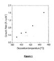
The results obtained in terms of growth rate for thin films deposited by ALD, in the 390°C - 450 °C temperature range, from (Cp)Ta(=NtBu)(NEt2)2 and ammonia are shown infigure 1 .
A step coverage of 100% is achieved for thin films deposited on substrates with 3D architectures. The bottoms such as the sidewalls are conformaly and uniformly recovered. - Therefore, the method disclosed in the present invention allows to deposit tantalum carbo-nitride on structures with high aspect ratio, which was not possible with the same precursor by using conventional deposition technique.
- TaCp(=NtBu)(NEt2)2 is stored into a container. The container is heated at 120°C and N2 is used as carrier gas at a flow of 50 sccm. Ammonia (NH3) is used as nitrogen source. The substrate is heated at 400°C. The precursor is sequentially introduced into the reaction chamber with trimethyl aluminium (TMA) and NH3: during the first step a pulse of TaCp(=NtBu)(NEt2)2 is introduced during about 8 seconds, followed by a 13 seconds N2 purge. A pulse of trimethyl aluminium (TMA) is then introduced into the reaction chamber during about 8 seconds, followed by a 13 seconds N2 purge. A pulse of NH3 is then introduced into the reaction chamber during 8 seconds, followed by a 13 seconds N2 purge. The first step is then done again. 400 cycles are performed this way. A film of tantalum nitride is obtained.
- TaCp(=NtBu)(NEt2)2 is stored into a container. The container is heated at 120°C and N2 is used as carrier gas at a flow of 50 sccm. Ozone (O3) is used as oxygen source. The substrate is heated at 400°C. The precursor is sequentially introduced into the reaction chamber with O3: during the first step a pulse of TaCp(=NtBu)(NEt2)2 is introduced during about 8 seconds, followed by a 13 seconds N2 purge. A pulse of O3 is then introduced into the reaction chamber during 8 seconds, followed by a 13 seconds N2 purge. The first step is then done again. 400 cycles are performed this way. A film of tantalum oxy-nitride is obtained.
Claims (12)
- A method for forming a tantalum-containing layer on a substrate, the method comprising at least the steps of:a) providing a vapor comprising at least one precursor compound of the formula Cp(R1)mTa(NR2 2)2(=NR3) (I):
 R1 is an organic ligand, each one independently selected in the group consisting of H, linear or branched hydrocarbyl radical comprising from 1 to 6 carbon atoms;R2 is an organic ligand, each one independently selected in the group consisting of H, linear or branched hydrocarbyl radical comprising from 1 to 6 carbon atoms;R3 is an organic ligand selected in the group consisting of H, linear or branched hydrocarbyl radical comprising from 1 to 6 carbon atoms;b) reacting the vapor comprising the at least one compound of formula (I) with the substrate, according to an atomic layer deposition process, to form a layer of a tantalum-containing complex on at least one surface of said substrate.
 - The method of claim 1 further comprising the step:c) reaction of the complex formed obtained in step b) with a reagent selected from another metal source, reducing reactants and/or nitriding reactants and/or oxidizing reactants.
- The method of one of claim 1 or 2 wherein:R1 is selected in the group consisting of H, an alkyl comprising from 1 to 4 carbon atoms, preferably, R1 is methyl or ethyl or isopropyl or tert-butyl;R2 is an alkyl comprising from 1 to 3 carbon atom, more preferably, R2 is an alkyl with 1 or 2 carbon atom; andR3 is alkyl with 3 or 4 carbon atoms, more preferably, R3 is isopropyl or tert-butyl.
- The method of one of claims 1 to 3 wherein each R1 are different from one another and each R2 are different from one another.
- The method of one of claims 1 to 4 wherein the vapour provided in step a) further comprises one or more metal (M')-organic precursor(s) to produce thin films containing tantalum and M'.
- The method of one of claims 1 to 5, wherein m = 0 in the formula (I).
- The method of one of claims 1 to 6, further comprising providing at least one reaction gas wherein the at least one reaction gas is selected from the group consisting of hydrogen, hydrogen sulfide, hydrogen selenide, hydrogen telluride, carbon monoxide, ammonia, organic amine, silane, disilane, higher silanes, silylamines, diborane, hydrazine, methylhydrazine, chlorosilane and chloropolysilane, metal alkyl, arsine, phosphine, trialkylboron, oxygen, ozone, water, hydrogen peroxide, nitrous oxide, nitrogen monoxide, nitrogen dioxide, alcohols, plasma comprising fragments of those species, and combinations thereof, preferably ozone or water.
- The method of one of claims 1 to 7, wherein the tantalum precursor of formula (I) is selected in the group consisting of:(Cp)Ta(=NtBu)(NEt2)2;(Cp)Ta(=NtBu)(NMe2)2;(Cp)Ta(=NC5H11)(NMe2)2;(Cp)Ta(=NtBu)(N(EtMe)2)2;(Cp)Ta(=NiPr)(NEt2)2;(Cp)Ta(=NiPr)(NMe2)2;(MeCp)Ta(=NtBu)(NMe2)2;(MeCp)Ta(=NiPr)(NMe2)2.
- The method of one of claims 1 to 8, wherein the temperature of the substrate is 25 °C to 450 °C, preferably 380°C to 425°C.
- The method of claim 9, wherein the atomic layer deposition chamber containing the substrate has a pressure of 0.133 Pa to 133 kPa, preferably below 27 kPa.
- The method of one of claims 1 to 9 further comprising the step of purging excess vapor comprising the at least one compound of formula (I) from the substrate, with an inert gas selected from the group consisting of hydrogen, nitrogen, helium, argon, and mixtures thereof.
- A method of manufacturing a semiconductor structure, comprising the steps of the method defined in any one of claims 1 to 10, wherein the substrate is a semiconductor substrate.
Priority Applications (1)
| Application Number | Priority Date | Filing Date | Title |
|---|---|---|---|
| EP09780636.8A EP2310551B1 (en) | 2008-08-01 | 2009-07-15 | Method of forming a tantalum-containing layer on a substrate |
Applications Claiming Priority (3)
| Application Number | Priority Date | Filing Date | Title |
|---|---|---|---|
| EP08305444 | 2008-08-01 | ||
| EP09780636.8A EP2310551B1 (en) | 2008-08-01 | 2009-07-15 | Method of forming a tantalum-containing layer on a substrate |
| PCT/EP2009/059067 WO2010012595A1 (en) | 2008-08-01 | 2009-07-15 | Method of forming a tantalum-containing layer on a substrate |
Publications (2)
| Publication Number | Publication Date |
|---|---|
| EP2310551A1 EP2310551A1 (en) | 2011-04-20 |
| EP2310551B1 true EP2310551B1 (en) | 2014-04-02 |
Family
ID=40091873
Family Applications (1)
| Application Number | Title | Priority Date | Filing Date |
|---|---|---|---|
| EP09780636.8A Active EP2310551B1 (en) | 2008-08-01 | 2009-07-15 | Method of forming a tantalum-containing layer on a substrate |
Country Status (6)
| Country | Link |
|---|---|
| US (1) | US9085823B2 (en) |
| EP (1) | EP2310551B1 (en) |
| JP (1) | JP5639055B2 (en) |
| KR (1) | KR101589777B1 (en) |
| CN (1) | CN102112654B (en) |
| WO (1) | WO2010012595A1 (en) |
Families Citing this family (7)
| Publication number | Priority date | Publication date | Assignee | Title |
|---|---|---|---|---|
| EP1916253A1 (en) * | 2006-10-26 | 2008-04-30 | L'AIR LIQUIDE, Société Anonyme pour l'Etude et l'Exploitation des Procédés Georges Claude | New group V metal containing precursors and their use for metal containing film deposition |
| EP2174942B1 (en) * | 2008-10-07 | 2011-11-30 | L'Air Liquide Société Anonyme pour l'Etude et l'Exploitation des Procédés Georges Claude | Niobium and vanadium organometallic precursors for thin film deposition |
| TWI551708B (en) * | 2011-07-22 | 2016-10-01 | 應用材料股份有限公司 | Method of atomic layer deposition using metal precursors |
| KR102627456B1 (en) * | 2015-12-21 | 2024-01-19 | 삼성전자주식회사 | Tantalum compound and methods of forming thin film and integrated circuit device |
| WO2018048124A1 (en) | 2016-09-08 | 2018-03-15 | 주식회사 유피케미칼 | Group 5 metal compound, preparation method therefor, film deposition precursor composition comprising same, and film deposition method using same |
| CN111534808A (en) * | 2020-05-19 | 2020-08-14 | 合肥安德科铭半导体科技有限公司 | Atomic layer deposition method of Ta-containing film and product thereof |
| KR102530814B1 (en) * | 2020-06-30 | 2023-05-10 | 주식회사 이지티엠 | Group 5 metal compound for thin film deposition and method of forming group 5 metal containing thin film using the same |
Family Cites Families (34)
| Publication number | Priority date | Publication date | Assignee | Title |
|---|---|---|---|---|
| IT1271025B (en) | 1994-10-20 | 1997-05-26 | Patreca Srl | VALVE FOR HIGH PRESSURE CYLINDERS WITH DEVICE FOR MAINTAINING RESIDUAL EMPTYING PRESSURE |
| US6010969A (en) | 1996-10-02 | 2000-01-04 | Micron Technology, Inc. | Method of depositing films on semiconductor devices by using carboxylate complexes |
| US6015917A (en) | 1998-01-23 | 2000-01-18 | Advanced Technology Materials, Inc. | Tantalum amide precursors for deposition of tantalum nitride on a substrate |
| US6616972B1 (en) * | 1999-02-24 | 2003-09-09 | Air Products And Chemicals, Inc. | Synthesis of metal oxide and oxynitride |
| US6268288B1 (en) | 1999-04-27 | 2001-07-31 | Tokyo Electron Limited | Plasma treated thermal CVD of TaN films from tantalum halide precursors |
| US6743473B1 (en) | 2000-02-16 | 2004-06-01 | Applied Materials, Inc. | Chemical vapor deposition of barriers from novel precursors |
| EP2293322A1 (en) * | 2000-06-08 | 2011-03-09 | Genitech, Inc. | Method for forming a metal nitride layer |
| US6491978B1 (en) | 2000-07-10 | 2002-12-10 | Applied Materials, Inc. | Deposition of CVD layers for copper metallization using novel metal organic chemical vapor deposition (MOCVD) precursors |
| WO2002020870A1 (en) | 2000-09-08 | 2002-03-14 | Applied Materials, Inc. | Chemical vapor deposition of tantalum oxide using oxygen-free liquid precursors |
| KR100814980B1 (en) | 2000-09-28 | 2008-03-18 | 프레지던트 앤드 펠로우즈 오브 하바드 칼리지 | Vapor deposition of oxides, silicates, and phosphates |
| JP3963078B2 (en) | 2000-12-25 | 2007-08-22 | 株式会社高純度化学研究所 | Tertiary amylimidotris (dimethylamido) tantalum, method for producing the same, raw material solution for MOCVD using the same, and method for forming a tantalum nitride film using the same |
| US7098131B2 (en) | 2001-07-19 | 2006-08-29 | Samsung Electronics Co., Ltd. | Methods for forming atomic layers and thin films including tantalum nitride and devices including the same |
| US7186385B2 (en) | 2002-07-17 | 2007-03-06 | Applied Materials, Inc. | Apparatus for providing gas to a processing chamber |
| WO2005002007A2 (en) | 2003-03-20 | 2005-01-06 | The Research Foundation Of State University Of Newyork | Process for producing semiconductor nanocrystal cores, core-shell, core-buffer-shell, and multiple layer systems in a non-coordinating solvent utilizing in situ surfactant generation |
| US7378129B2 (en) * | 2003-08-18 | 2008-05-27 | Micron Technology, Inc. | Atomic layer deposition methods of forming conductive metal nitride comprising layers |
| JP2005132756A (en) * | 2003-10-29 | 2005-05-26 | Tosoh Corp | Tantalum compound, method for producing the same and method for forming tantalum-containing thin film |
| JP2005132757A (en) | 2003-10-29 | 2005-05-26 | Tosoh Corp | Tantalum compound, method for producing the same and method for forming tantalum-containing thin film |
| KR20050091488A (en) * | 2004-03-12 | 2005-09-15 | 주식회사 유피케미칼 | The precursor compounds for the metal and ceramic film, and the method of synthesis |
| CN100576474C (en) * | 2004-07-20 | 2009-12-30 | 应用材料股份有限公司 | The ald that contains tantalum material with tantalum predecessor TAIMATA |
| JP5053543B2 (en) * | 2005-02-02 | 2012-10-17 | 東ソー株式会社 | Tantalum compound, production method thereof, tantalum-containing thin film, and formation method thereof |
| US20060182885A1 (en) * | 2005-02-14 | 2006-08-17 | Xinjian Lei | Preparation of metal silicon nitride films via cyclic deposition |
| US7348445B2 (en) | 2005-02-14 | 2008-03-25 | Praxair Technology, Inc. | Organoaluminum precursor compounds |
| US7314835B2 (en) | 2005-03-21 | 2008-01-01 | Tokyo Electron Limited | Plasma enhanced atomic layer deposition system and method |
| US7402517B2 (en) * | 2005-03-31 | 2008-07-22 | Battelle Memorial Institute | Method and apparatus for selective deposition of materials to surfaces and substrates |
| JP5096016B2 (en) | 2006-02-14 | 2012-12-12 | 東ソー株式会社 | Tantalum compound and method for producing the same, tantalum-containing thin film using the same and method for forming the same |
| US7959985B2 (en) | 2006-03-20 | 2011-06-14 | Tokyo Electron Limited | Method of integrating PEALD Ta-containing films into Cu metallization |
| US7482289B2 (en) | 2006-08-25 | 2009-01-27 | Battelle Memorial Institute | Methods and apparatus for depositing tantalum metal films to surfaces and substrates |
| US8795771B2 (en) * | 2006-10-27 | 2014-08-05 | Sean T. Barry | ALD of metal-containing films using cyclopentadienyl compounds |
| US8617301B2 (en) | 2007-01-30 | 2013-12-31 | Lam Research Corporation | Compositions and methods for forming and depositing metal films on semiconductor substrates using supercritical solvents |
| US20080248648A1 (en) | 2007-04-06 | 2008-10-09 | Thompson David M | Deposition precursors for semiconductor applications |
| KR100998417B1 (en) * | 2007-08-20 | 2010-12-03 | 주식회사 하이닉스반도체 | Method of forming a dielectric layer in semiconductor memory device |
| KR100884589B1 (en) | 2007-11-02 | 2009-02-19 | 주식회사 하이닉스반도체 | Multi phase clock generator and generating method |
| EP2065390A1 (en) | 2007-11-30 | 2009-06-03 | L'AIR LIQUIDE, Société Anonyme pour l'Etude et l'Exploitation des Procédés Georges Claude | Metal organic compounds containing an amidinate ligand and their use for vapour phase deposition of metal containing thin films |
| EP2707375A4 (en) * | 2011-05-13 | 2015-01-07 | Greenct Canada | Group 11 mono-metallic precursor compounds and use thereof in metal deposition |
-
2009
- 2009-07-15 JP JP2011520419A patent/JP5639055B2/en active Active
- 2009-07-15 CN CN200980130303.2A patent/CN102112654B/en active Active
- 2009-07-15 KR KR1020117002424A patent/KR101589777B1/en active IP Right Grant
- 2009-07-15 WO PCT/EP2009/059067 patent/WO2010012595A1/en active Application Filing
- 2009-07-15 US US13/056,934 patent/US9085823B2/en active Active
- 2009-07-15 EP EP09780636.8A patent/EP2310551B1/en active Active
Also Published As
| Publication number | Publication date |
|---|---|
| US9085823B2 (en) | 2015-07-21 |
| EP2310551A1 (en) | 2011-04-20 |
| JP2011530002A (en) | 2011-12-15 |
| CN102112654B (en) | 2013-03-20 |
| KR101589777B1 (en) | 2016-01-28 |
| WO2010012595A1 (en) | 2010-02-04 |
| KR20110041498A (en) | 2011-04-21 |
| CN102112654A (en) | 2011-06-29 |
| US20110244681A1 (en) | 2011-10-06 |
| JP5639055B2 (en) | 2014-12-10 |
Similar Documents
| Publication | Publication Date | Title |
|---|---|---|
| EP2174942B1 (en) | Niobium and vanadium organometallic precursors for thin film deposition | |
| TWI432597B (en) | Plasma enhanced cyclic deposition method of metal silicon nitride film | |
| EP2910665A1 (en) | Volatile dihydropyrazinyl and dihydropyrazine metal complexes | |
| EP2644741A1 (en) | Methods of preparing titanium containing thin films by atomic layer deposition using monocyclopentadienyl titanium-based precursors | |
| WO2017143246A1 (en) | Deposition of molybdenum thin films using a molybdenum carbonyl precursor | |
| KR100975687B1 (en) | Cyclic chemical vapor deposition of metal-silicon containing films | |
| EP2310551B1 (en) | Method of forming a tantalum-containing layer on a substrate | |
| US20140322924A1 (en) | Silicon containing compounds for ald deposition of metal silicate films | |
| KR101295031B1 (en) | Plasma enhanced cyclic deposition method of metal silicon nitride film | |
| EP2573096A1 (en) | Tantalum-organic compounds and their use for thin films deposition | |
| EP2808333A1 (en) | New tantalum precursors and their use | |
| WO2022226472A1 (en) | Deposition of vanadium-containing films | |
| KR20090107006A (en) | Plasma enhanced cyclic deposition method of metal silicon nitride film | |
| EP2808335A1 (en) | Vanadium precursors and their use | |
| EP2810949A1 (en) | Niobium precursors and their use | |
| EP2810950A1 (en) | Niobium-complexes and their use in a method for forming a niobium-containing layer on a substrate | |
| EP2808332A1 (en) | Tantalum precursors and their use | |
| EP2808336A1 (en) | New Vanadium precursors and their use | |
| EP2808331A1 (en) | Method for forming a tantalum-containing layer on a substrate | |
| EP2808334A1 (en) | Method for forming a vanadium-containing layer on a substrate | |
| EP2810948A1 (en) | Niobium-complexes and their use in a method for forming a niobium-containing layer on a substrate | |
| EP2902398A1 (en) | Niobium organic precursors and their use for vapor phase deposition of niobium containing films |
Legal Events
| Date | Code | Title | Description |
|---|---|---|---|
| PUAI | Public reference made under article 153(3) epc to a published international application that has entered the european phase |
Free format text: ORIGINAL CODE: 0009012 |
|
| 17P | Request for examination filed |
Effective date: 20110301 |
|
| AK | Designated contracting states |
Kind code of ref document: A1 Designated state(s): AT BE BG CH CY CZ DE DK EE ES FI FR GB GR HR HU IE IS IT LI LT LU LV MC MK MT NL NO PL PT RO SE SI SK SM TR |
|
| AX | Request for extension of the european patent |
Extension state: AL BA RS |
|
| DAX | Request for extension of the european patent (deleted) | ||
| GRAP | Despatch of communication of intention to grant a patent |
Free format text: ORIGINAL CODE: EPIDOSNIGR1 |
|
| INTG | Intention to grant announced |
Effective date: 20131023 |
|
| GRAS | Grant fee paid |
Free format text: ORIGINAL CODE: EPIDOSNIGR3 |
|
| GRAA | (expected) grant |
Free format text: ORIGINAL CODE: 0009210 |
|
| AK | Designated contracting states |
Kind code of ref document: B1 Designated state(s): AT BE BG CH CY CZ DE DK EE ES FI FR GB GR HR HU IE IS IT LI LT LU LV MC MK MT NL NO PL PT RO SE SI SK SM TR |
|
| REG | Reference to a national code |
Ref country code: GB Ref legal event code: FG4D |
|
| REG | Reference to a national code |
Ref country code: CH Ref legal event code: EP Ref country code: AT Ref legal event code: REF Ref document number: 660200 Country of ref document: AT Kind code of ref document: T Effective date: 20140415 |
|
| REG | Reference to a national code |
Ref country code: IE Ref legal event code: FG4D |
|
| REG | Reference to a national code |
Ref country code: DE Ref legal event code: R096 Ref document number: 602009022988 Country of ref document: DE Effective date: 20140515 |
|
| REG | Reference to a national code |
Ref country code: AT Ref legal event code: MK05 Ref document number: 660200 Country of ref document: AT Kind code of ref document: T Effective date: 20140402 |
|
| REG | Reference to a national code |
Ref country code: NL Ref legal event code: VDEP Effective date: 20140402 |
|
| REG | Reference to a national code |
Ref country code: LT Ref legal event code: MG4D |
|
| PG25 | Lapsed in a contracting state [announced via postgrant information from national office to epo] |
Ref country code: FI Free format text: LAPSE BECAUSE OF FAILURE TO SUBMIT A TRANSLATION OF THE DESCRIPTION OR TO PAY THE FEE WITHIN THE PRESCRIBED TIME-LIMIT Effective date: 20140402 Ref country code: CY Free format text: LAPSE BECAUSE OF FAILURE TO SUBMIT A TRANSLATION OF THE DESCRIPTION OR TO PAY THE FEE WITHIN THE PRESCRIBED TIME-LIMIT Effective date: 20140402 Ref country code: NO Free format text: LAPSE BECAUSE OF FAILURE TO SUBMIT A TRANSLATION OF THE DESCRIPTION OR TO PAY THE FEE WITHIN THE PRESCRIBED TIME-LIMIT Effective date: 20140702 Ref country code: BG Free format text: LAPSE BECAUSE OF FAILURE TO SUBMIT A TRANSLATION OF THE DESCRIPTION OR TO PAY THE FEE WITHIN THE PRESCRIBED TIME-LIMIT Effective date: 20140702 Ref country code: NL Free format text: LAPSE BECAUSE OF FAILURE TO SUBMIT A TRANSLATION OF THE DESCRIPTION OR TO PAY THE FEE WITHIN THE PRESCRIBED TIME-LIMIT Effective date: 20140402 Ref country code: IS Free format text: LAPSE BECAUSE OF FAILURE TO SUBMIT A TRANSLATION OF THE DESCRIPTION OR TO PAY THE FEE WITHIN THE PRESCRIBED TIME-LIMIT Effective date: 20140802 Ref country code: GR Free format text: LAPSE BECAUSE OF FAILURE TO SUBMIT A TRANSLATION OF THE DESCRIPTION OR TO PAY THE FEE WITHIN THE PRESCRIBED TIME-LIMIT Effective date: 20140703 Ref country code: LT Free format text: LAPSE BECAUSE OF FAILURE TO SUBMIT A TRANSLATION OF THE DESCRIPTION OR TO PAY THE FEE WITHIN THE PRESCRIBED TIME-LIMIT Effective date: 20140402 Ref country code: CZ Free format text: LAPSE BECAUSE OF FAILURE TO SUBMIT A TRANSLATION OF THE DESCRIPTION OR TO PAY THE FEE WITHIN THE PRESCRIBED TIME-LIMIT Effective date: 20140402 |
|
| PG25 | Lapsed in a contracting state [announced via postgrant information from national office to epo] |
Ref country code: ES Free format text: LAPSE BECAUSE OF FAILURE TO SUBMIT A TRANSLATION OF THE DESCRIPTION OR TO PAY THE FEE WITHIN THE PRESCRIBED TIME-LIMIT Effective date: 20140402 Ref country code: AT Free format text: LAPSE BECAUSE OF FAILURE TO SUBMIT A TRANSLATION OF THE DESCRIPTION OR TO PAY THE FEE WITHIN THE PRESCRIBED TIME-LIMIT Effective date: 20140402 Ref country code: PL Free format text: LAPSE BECAUSE OF FAILURE TO SUBMIT A TRANSLATION OF THE DESCRIPTION OR TO PAY THE FEE WITHIN THE PRESCRIBED TIME-LIMIT Effective date: 20140402 Ref country code: SE Free format text: LAPSE BECAUSE OF FAILURE TO SUBMIT A TRANSLATION OF THE DESCRIPTION OR TO PAY THE FEE WITHIN THE PRESCRIBED TIME-LIMIT Effective date: 20140402 Ref country code: HR Free format text: LAPSE BECAUSE OF FAILURE TO SUBMIT A TRANSLATION OF THE DESCRIPTION OR TO PAY THE FEE WITHIN THE PRESCRIBED TIME-LIMIT Effective date: 20140402 Ref country code: LV Free format text: LAPSE BECAUSE OF FAILURE TO SUBMIT A TRANSLATION OF THE DESCRIPTION OR TO PAY THE FEE WITHIN THE PRESCRIBED TIME-LIMIT Effective date: 20140402 |
|
| PG25 | Lapsed in a contracting state [announced via postgrant information from national office to epo] |
Ref country code: PT Free format text: LAPSE BECAUSE OF FAILURE TO SUBMIT A TRANSLATION OF THE DESCRIPTION OR TO PAY THE FEE WITHIN THE PRESCRIBED TIME-LIMIT Effective date: 20140804 |
|
| REG | Reference to a national code |
Ref country code: DE Ref legal event code: R097 Ref document number: 602009022988 Country of ref document: DE |
|
| PG25 | Lapsed in a contracting state [announced via postgrant information from national office to epo] |
Ref country code: DK Free format text: LAPSE BECAUSE OF FAILURE TO SUBMIT A TRANSLATION OF THE DESCRIPTION OR TO PAY THE FEE WITHIN THE PRESCRIBED TIME-LIMIT Effective date: 20140402 Ref country code: RO Free format text: LAPSE BECAUSE OF FAILURE TO SUBMIT A TRANSLATION OF THE DESCRIPTION OR TO PAY THE FEE WITHIN THE PRESCRIBED TIME-LIMIT Effective date: 20140402 Ref country code: EE Free format text: LAPSE BECAUSE OF FAILURE TO SUBMIT A TRANSLATION OF THE DESCRIPTION OR TO PAY THE FEE WITHIN THE PRESCRIBED TIME-LIMIT Effective date: 20140402 Ref country code: SK Free format text: LAPSE BECAUSE OF FAILURE TO SUBMIT A TRANSLATION OF THE DESCRIPTION OR TO PAY THE FEE WITHIN THE PRESCRIBED TIME-LIMIT Effective date: 20140402 Ref country code: BE Free format text: LAPSE BECAUSE OF FAILURE TO SUBMIT A TRANSLATION OF THE DESCRIPTION OR TO PAY THE FEE WITHIN THE PRESCRIBED TIME-LIMIT Effective date: 20140402 |
|
| PLBE | No opposition filed within time limit |
Free format text: ORIGINAL CODE: 0009261 |
|
| STAA | Information on the status of an ep patent application or granted ep patent |
Free format text: STATUS: NO OPPOSITION FILED WITHIN TIME LIMIT |
|
| PG25 | Lapsed in a contracting state [announced via postgrant information from national office to epo] |
Ref country code: LU Free format text: LAPSE BECAUSE OF FAILURE TO SUBMIT A TRANSLATION OF THE DESCRIPTION OR TO PAY THE FEE WITHIN THE PRESCRIBED TIME-LIMIT Effective date: 20140715 |
|
| REG | Reference to a national code |
Ref country code: CH Ref legal event code: PL |
|
| 26N | No opposition filed |
Effective date: 20150106 |
|
| GBPC | Gb: european patent ceased through non-payment of renewal fee |
Effective date: 20140715 |
|
| PG25 | Lapsed in a contracting state [announced via postgrant information from national office to epo] |
Ref country code: IT Free format text: LAPSE BECAUSE OF FAILURE TO SUBMIT A TRANSLATION OF THE DESCRIPTION OR TO PAY THE FEE WITHIN THE PRESCRIBED TIME-LIMIT Effective date: 20140402 |
|
| REG | Reference to a national code |
Ref country code: DE Ref legal event code: R097 Ref document number: 602009022988 Country of ref document: DE Effective date: 20150106 |
|
| REG | Reference to a national code |
Ref country code: IE Ref legal event code: MM4A |
|
| PG25 | Lapsed in a contracting state [announced via postgrant information from national office to epo] |
Ref country code: CH Free format text: LAPSE BECAUSE OF NON-PAYMENT OF DUE FEES Effective date: 20140731 Ref country code: LI Free format text: LAPSE BECAUSE OF NON-PAYMENT OF DUE FEES Effective date: 20140731 |
|
| PG25 | Lapsed in a contracting state [announced via postgrant information from national office to epo] |
Ref country code: GB Free format text: LAPSE BECAUSE OF NON-PAYMENT OF DUE FEES Effective date: 20140715 |
|
| PG25 | Lapsed in a contracting state [announced via postgrant information from national office to epo] |
Ref country code: SI Free format text: LAPSE BECAUSE OF FAILURE TO SUBMIT A TRANSLATION OF THE DESCRIPTION OR TO PAY THE FEE WITHIN THE PRESCRIBED TIME-LIMIT Effective date: 20140402 |
|
| PG25 | Lapsed in a contracting state [announced via postgrant information from national office to epo] |
Ref country code: IE Free format text: LAPSE BECAUSE OF NON-PAYMENT OF DUE FEES Effective date: 20140715 |
|
| PG25 | Lapsed in a contracting state [announced via postgrant information from national office to epo] |
Ref country code: MC Free format text: LAPSE BECAUSE OF FAILURE TO SUBMIT A TRANSLATION OF THE DESCRIPTION OR TO PAY THE FEE WITHIN THE PRESCRIBED TIME-LIMIT Effective date: 20140402 Ref country code: SM Free format text: LAPSE BECAUSE OF FAILURE TO SUBMIT A TRANSLATION OF THE DESCRIPTION OR TO PAY THE FEE WITHIN THE PRESCRIBED TIME-LIMIT Effective date: 20140402 |
|
| PG25 | Lapsed in a contracting state [announced via postgrant information from national office to epo] |
Ref country code: MT Free format text: LAPSE BECAUSE OF FAILURE TO SUBMIT A TRANSLATION OF THE DESCRIPTION OR TO PAY THE FEE WITHIN THE PRESCRIBED TIME-LIMIT Effective date: 20140402 |
|
| REG | Reference to a national code |
Ref country code: FR Ref legal event code: PLFP Year of fee payment: 8 |
|
| PG25 | Lapsed in a contracting state [announced via postgrant information from national office to epo] |
Ref country code: TR Free format text: LAPSE BECAUSE OF FAILURE TO SUBMIT A TRANSLATION OF THE DESCRIPTION OR TO PAY THE FEE WITHIN THE PRESCRIBED TIME-LIMIT Effective date: 20140402 Ref country code: HU Free format text: LAPSE BECAUSE OF FAILURE TO SUBMIT A TRANSLATION OF THE DESCRIPTION OR TO PAY THE FEE WITHIN THE PRESCRIBED TIME-LIMIT; INVALID AB INITIO Effective date: 20090715 |
|
| REG | Reference to a national code |
Ref country code: FR Ref legal event code: PLFP Year of fee payment: 9 |
|
| PG25 | Lapsed in a contracting state [announced via postgrant information from national office to epo] |
Ref country code: MK Free format text: LAPSE BECAUSE OF FAILURE TO SUBMIT A TRANSLATION OF THE DESCRIPTION OR TO PAY THE FEE WITHIN THE PRESCRIBED TIME-LIMIT Effective date: 20140402 |
|
| REG | Reference to a national code |
Ref country code: FR Ref legal event code: PLFP Year of fee payment: 10 |
|
| PGFP | Annual fee paid to national office [announced via postgrant information from national office to epo] |
Ref country code: FR Payment date: 20230725 Year of fee payment: 15 Ref country code: DE Payment date: 20230719 Year of fee payment: 15 |