EP2309644A1 - Large time constant steering circuit and instrumentation amplifier implementing same - Google Patents
Large time constant steering circuit and instrumentation amplifier implementing same Download PDFInfo
- Publication number
- EP2309644A1 EP2309644A1 EP11151396A EP11151396A EP2309644A1 EP 2309644 A1 EP2309644 A1 EP 2309644A1 EP 11151396 A EP11151396 A EP 11151396A EP 11151396 A EP11151396 A EP 11151396A EP 2309644 A1 EP2309644 A1 EP 2309644A1
- Authority
- EP
- European Patent Office
- Prior art keywords
- input
- current
- voltage
- output
- time constant
- Prior art date
- Legal status (The legal status is an assumption and is not a legal conclusion. Google has not performed a legal analysis and makes no representation as to the accuracy of the status listed.)
- Granted
Links
Images



Classifications
-
- H—ELECTRICITY
- H03—ELECTRONIC CIRCUITRY
- H03H—IMPEDANCE NETWORKS, e.g. RESONANT CIRCUITS; RESONATORS
- H03H1/00—Constructional details of impedance networks whose electrical mode of operation is not specified or applicable to more than one type of network
- H03H1/02—RC networks, e.g. filters
-
- A—HUMAN NECESSITIES
- A61—MEDICAL OR VETERINARY SCIENCE; HYGIENE
- A61B—DIAGNOSIS; SURGERY; IDENTIFICATION
- A61B5/00—Measuring for diagnostic purposes; Identification of persons
- A61B5/24—Detecting, measuring or recording bioelectric or biomagnetic signals of the body or parts thereof
- A61B5/30—Input circuits therefor
- A61B5/307—Input circuits therefor specially adapted for particular uses
- A61B5/31—Input circuits therefor specially adapted for particular uses for electroencephalography [EEG]
-
- H—ELECTRICITY
- H03—ELECTRONIC CIRCUITRY
- H03F—AMPLIFIERS
- H03F3/00—Amplifiers with only discharge tubes or only semiconductor devices as amplifying elements
- H03F3/38—DC amplifiers with modulator at input and demodulator at output; Modulators or demodulators specially adapted for use in such amplifiers
- H03F3/387—DC amplifiers with modulator at input and demodulator at output; Modulators or demodulators specially adapted for use in such amplifiers with semiconductor devices only
-
- H—ELECTRICITY
- H03—ELECTRONIC CIRCUITRY
- H03F—AMPLIFIERS
- H03F3/00—Amplifiers with only discharge tubes or only semiconductor devices as amplifying elements
- H03F3/45—Differential amplifiers
- H03F3/45071—Differential amplifiers with semiconductor devices only
- H03F3/45076—Differential amplifiers with semiconductor devices only characterised by the way of implementation of the active amplifying circuit in the differential amplifier
- H03F3/45179—Differential amplifiers with semiconductor devices only characterised by the way of implementation of the active amplifying circuit in the differential amplifier using MOSFET transistors as the active amplifying circuit
- H03F3/45183—Long tailed pairs
- H03F3/45188—Non-folded cascode stages
-
- H—ELECTRICITY
- H03—ELECTRONIC CIRCUITRY
- H03F—AMPLIFIERS
- H03F3/00—Amplifiers with only discharge tubes or only semiconductor devices as amplifying elements
- H03F3/45—Differential amplifiers
- H03F3/45071—Differential amplifiers with semiconductor devices only
- H03F3/45076—Differential amplifiers with semiconductor devices only characterised by the way of implementation of the active amplifying circuit in the differential amplifier
- H03F3/45475—Differential amplifiers with semiconductor devices only characterised by the way of implementation of the active amplifying circuit in the differential amplifier using IC blocks as the active amplifying circuit
-
- H—ELECTRICITY
- H03—ELECTRONIC CIRCUITRY
- H03F—AMPLIFIERS
- H03F3/00—Amplifiers with only discharge tubes or only semiconductor devices as amplifying elements
- H03F3/45—Differential amplifiers
- H03F3/45071—Differential amplifiers with semiconductor devices only
- H03F3/45479—Differential amplifiers with semiconductor devices only characterised by the way of common mode signal rejection
-
- H—ELECTRICITY
- H03—ELECTRONIC CIRCUITRY
- H03F—AMPLIFIERS
- H03F2200/00—Indexing scheme relating to amplifiers
- H03F2200/261—Amplifier which being suitable for instrumentation applications
-
- H—ELECTRICITY
- H03—ELECTRONIC CIRCUITRY
- H03F—AMPLIFIERS
- H03F2203/00—Indexing scheme relating to amplifiers with only discharge tubes or only semiconductor devices as amplifying elements covered by H03F3/00
- H03F2203/45—Indexing scheme relating to differential amplifiers
- H03F2203/45136—One differential amplifier in IC-block form being shown
-
- H—ELECTRICITY
- H03—ELECTRONIC CIRCUITRY
- H03F—AMPLIFIERS
- H03F2203/00—Indexing scheme relating to amplifiers with only discharge tubes or only semiconductor devices as amplifying elements covered by H03F3/00
- H03F2203/45—Indexing scheme relating to differential amplifiers
- H03F2203/45424—Indexing scheme relating to differential amplifiers the CMCL comprising a comparator circuit
-
- H—ELECTRICITY
- H03—ELECTRONIC CIRCUITRY
- H03F—AMPLIFIERS
- H03F2203/00—Indexing scheme relating to amplifiers with only discharge tubes or only semiconductor devices as amplifying elements covered by H03F3/00
- H03F2203/45—Indexing scheme relating to differential amplifiers
- H03F2203/45438—Indexing scheme relating to differential amplifiers the CMCL uses digital signals
-
- H—ELECTRICITY
- H03—ELECTRONIC CIRCUITRY
- H03F—AMPLIFIERS
- H03F2203/00—Indexing scheme relating to amplifiers with only discharge tubes or only semiconductor devices as amplifying elements covered by H03F3/00
- H03F2203/45—Indexing scheme relating to differential amplifiers
- H03F2203/45441—Indexing scheme relating to differential amplifiers the CMCL comprising an integrating circuit
Definitions
- the present invention relates to a large time constant steering circuit for slowly changing a voltage on a node between at least two discrete voltage levels.
- the present invention further relates to a slow steering current DAC comprising said large time constant steering circuit.
- the present invention further relates to an instrumentation amplifier device comprising a current balancing instrumentation amplifier for amplifying an input signal to an amplified output signal and a DC servo-loop for removing a DC-component from the input signal.
- the present invention further relates to an EEG acquisition ASIC comprising said instrumentation amplifier device.
- a coarse servo-loop and a fine servo-loop can be used.
- the coarse servo-loop has discrete output levels where as the fine servo-loop has a continuous output range. Therefore, the output range of the fine servo-loop in the prior implementation can be reduced while the coarse-fine servo-loop is still capable of supplying the same output range.
- the implementation of the coarse amplifier is critical such that the time constant of the output of the coarse servo-loop must be much slower than the (1/2 ⁇ f HP ), where f HP is the high-pass filter cut-off frequency of the instrumentation amplifier that is defined by the fine servo-loop.
- f HP is the high-pass filter cut-off frequency of the instrumentation amplifier that is defined by the fine servo-loop.
- the crucial need is to implement a large-time constant inside the coarse servo-loop so that the output of the coarse servo-loop changes very slowly, when it updates its output.
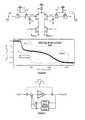
- Figure 1A uses an on-chip resistor, R1A, connected between the input, Vin1A, and the output, Vout1A, and an on-chip capacitor, C1A, connected between the output and the ground.
- R1A on-chip resistor
- C1A on-chip capacitor
- Figure 1B shows the realization of a large time constant where the resistors are implemented by using pseudo resistors [3].
- Figure 1C shows the realization of a large time constant where the resistors are implemented using the structure proposed in [4].
- Both approaches can occupy very small area, however, they suffer from the fact that the input voltage swing is only limited to less than hundred millivolts. This is due to the fact that the PMOS transistors of Figure 1B and Figure 1C operate in weak inversion, and a large input signal will increase the source-to-gate voltage of the PMOS transistors. This further turns on the transistor, leading to reduced time constant. Therefore, both the implementation of Figure 1B and Figure 1C needs the series connection of large number of transistors in order to improve their input range. This can lead to large silicon area consumption.
- DAC digital to analog conversion
- a large time constant steering circuit for slowly changing a voltage on a node between at least two discrete voltage levels.
- the circuit comprises an input node for receiving an input voltage, an output node for presenting an output voltage, a capacitive part connected at said output node for providing said output voltage and a resistive part connected between said input and output nodes for conducting a charging current from said input node to said capacitive part or a discharging current from said capacitive part to said input node depending on said input voltage.
- the resistive part comprises a semiconductor structure connectable between said input node and said capacitive part in such a way that the semiconductor structure remains in a substantially nonconducting state (i.e. an OFF state) irrespective of the input and output voltages and passes only leakage currents for charging or discharging said capacitive part. So the capacitive part is charged and discharged by leakage currents only.
- the circuit is formed by two PMOS transistors and a capacitor.
- This circuit uses only passive components, occupies minimal area, has a wide input swing and does not consume any static power.
- the substrates of the PMOS transistors are preferably connected together, which are also connected to the sources of the PMOS transistors.
- the gates of the PMOS transistors can be tied to the supply voltage to prevent switching ON. Hence, the PMOS transistors can operate in their OFF state independent of the input voltage level. This is in contrast to implementations where the transistors are operating in weak inversion like in the prior art. Therefore, the circuit of this embodiment of the present invention will have a large time constant that is independent from the input voltage swing, whereas the other implementations are very sensitive to the input voltage swing.
- the large time constant steering circuit is used to implement an intentionally slow steering current digital-to-analog converter (DAC), which may in turn be used to implement a coarse servo-loop of an instrumentation amplifier with high-pass filter characteristics, in particular an AC coupled chopper stabilized instrumentation amplifier (ACCIA).
- DAC digital-to-analog converter
- ACCIA AC coupled chopper stabilized instrumentation amplifier
- the fine servo-loop of the ACCIA is preferably implemented by a transconductance stage.
- Figures 1A-1C show examples of the realization of a large time constant in the prior art.
- Figure 2 shows a preferred embodiment of a large time constant steering circuit according to the invention.
- Figure 3 illustrates the equivalent circuit of the circuit of figure 2 .
- Figure 4 describes the mechanisms that charge and discharge the load capacitance of the circuit of figure 2 .
- Figure 5 shows the implementation of an intentionally slow steering DAC according to the invention.
- Figure 6 illustrates the measurement from a slow steering DAC according to figure 5 ..
- FIG. 7 illustrates the conceptual implementation of an AC coupled chopper stabilized instrumentation amplifier (ACCIA) according to a preferred embodiment of the invention.
- ACCIA AC coupled chopper stabilized instrumentation amplifier
- Figure 8 illustrates a complete implementation of an ACCIA according to a preferred embodiment of the invention.
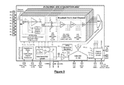
- Figure 9 illustrates an 8-channel EEG acquisition ASIC according to a preferred embodiment of the invention.
- the present invention includes a circuit that realizes a large time constant, which uses only passive components.
- the circuit occupies minimal area and does not consume any static power.
- the time constant of the circuit is minimally dependent on the input voltage swing.
- FIG. 2 A preferred embodiment of the circuit is illustrated in Figure 2 .
- the circuit comprises two PMOS transistors, M21 and M22, and a load capacitor, C2.
- the substrates of the PMOS transistors are connected together, which are also connected to the sources of the PMOS transistors.
- the gates of the PMOS transistors are tied to the supply voltage.
- the PMOS transistors are always operating in their OFF state independent of the input voltage level.
- This is in contrast to the implementations in Figure 1B and Figure 1C , where the transistors are operating in weak inversion.
- this is the main reason for the circuit of the present invention to have a large time constant that is independent from the input voltage swing, where as the implementations of Figure 1B and Figure 1C are very sensitive to the input voltage swing.
- the implementation assumes that the available technology is an n-well or a twin-well process.
- the same architecture can be implemented using NMOS transistors in a p-well or a twin-well process.
- a parasitic PNP bipolar transistor is created for each of the PMOS transistors by the drain, the n-well and the p-substrate of this PMOS transistor. Since the PMOS transistors are in OFF state, the only available path for the current to flow is through the parasitic PNP bipolar transistors, Q31 and Q32. Due to the fact that the source and the bulk connections of the PMOS transistors M31 and M32 are shorted, the bases of the parasitic PNP bipolar transistors Q31 and Q32 are also shorted. As a result, the two MOS transistors are equivalent to two base-to-base connected PNP bipolar transistors.
- Figure 4 describes the flow of current when a step voltage input is applied to the circuit that implements large time constant.
- Figure 4 describes the flow of current when a step voltage input is applied to the circuit that implements large time constant.
- the equivalent model of the implementation is presented, which is two base-to-base connected PNP bipolar transistors.
- the base-emitter diode of the PNP bipolar transistor Q41 is forward biased. This reduces the resistance between the input node and the common base of the PNP bipolar transistors Q41 and Q42.
- the base-emitter diode of the PNP bipolar transistor Q42 is reverse biased. Therefore, the only current that can charge the load capacitor C41 is the leakage current of the reverse biased base-emitter diode of the PNP bipolar transistor Q42. This charging continues till the voltage at Vout41 equals to the voltage of the common base of the bipolar transistors Q41 and Q42. This voltage is slightly lower than the input voltage due to the leakage current I leakage,BB , which is the leakage current of the reverse biased diode between the common base and the p-substrate.
- the two different leakage currents discharge the common base of the PNP bipolar transistors.
- the first leakage current is due to the reverse biased base-emitter diode of Q43, I leakage,BE
- the second current is the leakage current of the reverse biased diode between the common base of the PNP bipolar transistors and the p-substrate, I leakage,BB .
- the base-emitter diode of the PNP bipolar transistor, Q44 conducts.
- the voltage at Vout42 follows the voltage at the common base of the PNP bipolar transistors Q43 and Q44. Therefore, the load capacitance C42 is discharged by a total current of I leakage,BE +I leakage,BB .
- FIG. 5 shows the implementation of the slow steering current DAC.
- the realization consists of a current source, 15, two pass gates M51 and M52, and two cascade transistors, M53 and M54.
- the purpose of the cascade transistors is to increase the output impedance of the current DAC and to make DAC current independent of the output voltage.
- the two pass gates control the current passing through the each branch of the current DAC, namely, I DAC,L and I DAC,R , so that the tail current, 15, of the current DAC can be steered between the two branches.
- the voltages of the pass gates are each controlled by a large time constant steering circuit as described above.
- the steering time of the current DAC is defined by the large time constant implementations that involve the components M51A, M51 B and C51 for the left branch of the current DAC, and the components M52A, M52B and C52 for the right branch of the current DAC.
- the switches S51, S52, S55, and S56 control the input voltage to the large time constant implementations.
- the switches S53, S54, S57 and S58 control the gate voltages of the PMOS transistors M51A, M51 B, M52A, and M52B.
- the transistors M51A, M51 B, M52A, and M52B are connected to the supply voltage, then these transistors and the load capacitors C51 and C52 implements two large time constant circuits. If the gates of the transistors M51A, M51 B, M52A, and M52B are connected to the ground, then the transistors turn ON and fast steering of the current DAC can be realized.
- Figure 6 demonstrates the operation of the slow steering current DAC by measuring the output current difference between the left and the right braches, (l DAC,L -l DAC,R ).
- a step input with a rising edge from 1.8V to 3V is applied to the left input of the current DAC, and a step input with a falling edge from 3V to 1.8V is applied to the right input, simultaneously. Therefore, it should expected that the output current should steer from left to right, which equals to a decrease in (l DAC , L -I DAC,R ).
- the gates of the transistors M61A, M61 B, M62A, and M62B are connected to the supply voltage. Therefore, these transistors are turned OFF.
- the voltage at nodes VG61 and VG62 are controlled by the claimed large time constant implementation.
- the discharging current of the large time constant implementation is larger than the charging current, see Eq.(1). This indicates that the first phase of the DAC steering occurs mainly due to the discharge of capacitance C62 and the second phase occurs due to the charging of the capacitance C61.
- the total steering time is more than 1000 seconds when selecting C61 and C62 as 0.5pF, and the fastest part of the steering occurs in slower than 300 seconds. This proves the operation of the claimed large time constant implementation even under large input voltage swing as much as 1.2V.
- FIG. 7 illustrates the conceptual implementation of an ACCIA according to the invention.
- the high-pass filter characteristic is introduced to the ACCIA by utilizing a coarse servo-loop and a fine servo-loop.
- the fine servo-loop sets the cut-off frequency of the high-pass filter characteristics and supplies a continuous analog output.
- the coarse servo-loop has discrete output steps, where each step corresponds to the half of the output range of the fine servo-loop. Therefore, once the output of the fine servo-loop reaches its limit, the coarse DC servo-loop updates its output that sets the output of the fine servo-loop to its midrange.
- FIG. 8 illustrates the complete implementation of the ACCIA that utilizes the fine and coarse servo-loops for implementing high-pass filter characteristics.
- the core amplifier is a current balancing instrumentation amplifier (CBIA).
- CBIA current balancing instrumentation amplifier
- the operation of the core amplifier can be described as follows: the input voltage is copied to the terminals of R 1 . This voltage creates a current through R 1 that is supplied by the ACCIA. This current is sensed by the CBIA and the same current is supplied to R 2 . The current through R 2 creates the output voltage of the CBIA. Therefore, the gain of the CBIA is defined by the ratio of two resistors as R 2 /R 1 .
- a second gain stage with high-pass filter characteristics further amplifies the output of the CBIA and filters the offset voltage of the CBIA.
- the fine servo-loop and the coarse servo-loop are connected to the output of an on-chip integrator.
- the purpose of the on-chip integrator is to sense the output DC level of the amplifier.
- the fine servo-loop is implemented by a transconductance stage. If a DC input voltage is applied to the ACCIA, it is copied to the terminals of R 1 . Under steady state, the current through R 1 due to the DC input is supplied by the fine servo-loop. Since, the CBIA does not supply the current through R 1 , no current is copied to R 2 . This means that the DC input to the instrumentation amplifier is not amplified.
- the coarse DC servo-loop sense this and updates its output in such a way that the DC servo-loop can supply enough current to filter the input DC voltage to the instrumentation amplifier.
- the coarse servo-loop is implemented by using the slow steering DAC implementation of Figure 5 .
- the combination of 16 slow steering current DACs creates a 16-bit slow steering current DAC. Each bit of this current DAC is controlled by a thermometer code counter. Two comparators check weather the fine transconductance stage has reached its limit.
- the comparators of the coarse transconductance stage sense this and changes a bit of the 16-bit slow steering current DAC to increase I DAC , L and reduce I DAC,R .
- the tail current of each DAC bit is set to I fine .
- the coarse-fine combination of the transconductance stage can filter an input DC voltage of: I fine ⁇ M 2 + m DAC ⁇ I DAC ⁇ R 1 where m DAC is the number of DAC bits and I DAC is the tail current source of each DAC bit.
- the steering of the DAC is not much slower than the (1/2 ⁇ f HP ), where f hp is set by the integrator stage and the fine transconductance stage, and it must be in the rage of 0.1 Hz - 1 Hz for most of the biomedical signal acquisition applications, then the steering of the DAC would create a voltage step at the output of the instrumentation amplifier. This is undesired since it can saturate the output of the instrumentation amplifier.
- g m,fine is the transconductance of the input pair stage of the fine transconductance stage
- M is the mirror ratio of the fine transconductance stage
- a v , INT is the open loop gain of the on-chip integrator
- A is the gain of the second gain stage connected to the output of the CBIA
- f LP,INT is the low-pass corner frequency of the on-chip integrator.
- the result of this equation for the current implementation is 0.1Hz. Since even the fastest steering time of the slow steering DAC is 300 seconds, which is much slower that (1/2 ⁇ f HP ), the fine transconductance stage can prevent the step response at the output.
- the main advantage of using such fine-coarse architecture is the reduction of the current that is consumed in the fine transconductance stage. It should be noted that the current consumed in the input stage of the fine transconductance stage is wasted. On the other hand, the 16-bit slow steering current DAC actually supplies the bias current of the CBIA, therefore the increase in the DAC current also reduces the noise of the CBIA.
- this ACCIA is used as a front-end of a readout channel.
- the proposed circuit can for example be used in an EEG acquisition system.
- a complete EEG Acquisition ASIC can be designed (see Figure 9 ), where the outputs of the analog readout front-ends can be digitized using the on-chip low-power ADC. This eliminates the use of an external ADC that not only improves the power dissipation of the EEG acquisition system but also can shrink the system size.
- FIG. 9 shows the architecture of the proposed EEG acquisition ASIC.
- the main building blocks of the ASIC are: eight readout front-end channels, an 11-bit SAR ADC, a bias circuit, a 1 MHz relaxation oscillator, an electrode impedance measurement circuit, and a calibration signal generator.
- the readout front-end channels are responsible for extracting and conditioning the EEG signals from the biopotential electrodes.
- the preamplifier of a readout channel is the presented ACCIA.
- the ACCIA is followed by a chopping spike filter (CSF) stage, which includes a HPF with adjustable cut-off frequency. After the CSF stage a programmable gain stage further amplifies the extracted biopotential signals.
- the output of each channel is buffered and time-multiplexed.
- a class-AB buffer buffers the outputs of the channels and drives the input capacitance of the ADC.
- CSF chopping spike filter
- the ADC of the ASIC is implemented using the SAR-ADC architecture due to its low-power dissipation characteristics.
- the operating clock of the ADC is generated by the on-chip 1MHz relaxation oscillator.
- the operation of the relaxation oscillator is duty cycled such that it generates the 1MHz clock only when the ADC is asked to convert an analog input signal.
- the reference voltage of the ADC is generated by the bias circuit, and it is buffered by a class-AB buffer to drive the capacitive DAC of the SAR-ADC.
- the ASIC is designed for battery powered systems, where the supply voltage changes as the battery discharges. Therefore, the bias generator circuit of the ASIC uses a PTAT voltage generator to generate a temperature and supply independent reference voltage. This reference voltage is used to generate all the bias voltages and currents of the ASIC, as well as the reference voltage of the ADC. Additionally, it should be noted that the patient bias voltage that is used for the grounding of the patient is also generated by the bias generator circuit.
- the digital control circuit of the ASIC uses a 32kHz clock input from which the sample signals of the analog multiplexer is generated, and to which the operation of the ADC is synchronized.
- the sample time of the first channel of the ASIC can be used as a synchronization signal with an external microcontroller.
- the digital control circuit accepts a clock signal with 1ms pulse duration and 300s period. This clock is necessary for the operation of the coarse transconductance stage of the ACCIA.
- the coarse transconductance stage checks whether the fine transconductance stage has reached its limits. If so, the coarse transconductance stage adjusts its output accordingly.
- this slow operation of the coarse transconductance stage can make the start-up of the ACCIA circuit extremely slow. Therefore, the ASIC has a start-up mode.
- the ASIC includes an electrode impedance measurement and calibration modes, which enable the user to measure the impedances of the biopotential electrodes and to calibrate the matching of the readout front-end channels, respectively.
Landscapes
- Engineering & Computer Science (AREA)
- Power Engineering (AREA)
- Health & Medical Sciences (AREA)
- Life Sciences & Earth Sciences (AREA)
- Medical Informatics (AREA)
- Pathology (AREA)
- Biomedical Technology (AREA)
- Heart & Thoracic Surgery (AREA)
- Physics & Mathematics (AREA)
- Molecular Biology (AREA)
- Surgery (AREA)
- Animal Behavior & Ethology (AREA)
- General Health & Medical Sciences (AREA)
- Public Health (AREA)
- Veterinary Medicine (AREA)
- Biophysics (AREA)
- Amplifiers (AREA)
Abstract
Description
- The present invention relates to a large time constant steering circuit for slowly changing a voltage on a node between at least two discrete voltage levels. The present invention further relates to a slow steering current DAC comprising said large time constant steering circuit. The present invention further relates to an instrumentation amplifier device comprising a current balancing instrumentation amplifier for amplifying an input signal to an amplified output signal and a DC servo-loop for removing a DC-component from the input signal. The present invention further relates to an EEG acquisition ASIC comprising said instrumentation amplifier device.
- In order to remove the DC component of a signal or to eliminate DC offset, most integrated circuits rely on high-pass filters. Most commonly used examples of a high-pass filter are DC level shifters, DC blocking capacitors, and DC servo-loops.
- Recently, there is much interest to develop instrumentation amplifiers with low-power dissipation, low-noise, high common mode rejection, and large input impedance for example towards the field of ambulatory biomedical signal monitoring. The large DC component of the biomedical signals necessitates the implementation of high-pass filter characteristics to the instrumentation amplifier.
- These requirements lead to the usage of chopper-stabilized instrumentation amplifiers with high-pass filter characteristics [1], [2]. The most power efficient way of implementing high-pass filter characteristics to the chopper stabilized amplifiers is to use DC servo-loops [1], [2]. The DC servo-loop senses the DC level of the output and subtracts it from the input of the amplifier.
- The previous implementations of the chopper stabilized amplifiers incorporating a DC servo-loop for implementing high-pass filter characteristics either subtract voltage, [2], or current, [1], from the input signal before it is amplified by the instrumentation amplifier. However, the prior technique results in large power dissipation due to the fact that the DC servo-loop must be capable of supplying wide range of current output, and the later reduces the input impedance of the amplifier.
- In an attempt to reduce the power dissipation of a DC servo-loop that subtracts current from the input signal, a coarse servo-loop and a fine servo-loop can be used. The coarse servo-loop has discrete output levels where as the fine servo-loop has a continuous output range. Therefore, the output range of the fine servo-loop in the prior implementation can be reduced while the coarse-fine servo-loop is still capable of supplying the same output range.
- However, the implementation of the coarse amplifier is critical such that the time constant of the output of the coarse servo-loop must be much slower than the (1/2πfHP), where fHP is the high-pass filter cut-off frequency of the instrumentation amplifier that is defined by the fine servo-loop. In this case, the effect of the changing coarse servo-loop to the output of the instrumentation amplifier can be minimized by the fine servo-loop. Therefore, the crucial need is to implement a large-time constant inside the coarse servo-loop so that the output of the coarse servo-loop changes very slowly, when it updates its output.
- Large time constant implementations are presented in
Figure 1A, Figure 1B and Figure 1C. Figure 1A uses an on-chip resistor, R1A, connected between the input, Vin1A, and the output, Vout1A, and an on-chip capacitor, C1A, connected between the output and the ground. However, considering the necessity for a high-pass filter cut-off frequency in the range of 0.1 Hz to 1 Hz for most of the biomedical signal acquisition systems, the time constant of this architecture must be set much lower than 1/(2π(0.1Hz)), which leads to extremely large silicon area if implemented using architecture ofFigure 1A . -
Figure 1B shows the realization of a large time constant where the resistors are implemented by using pseudo resistors [3].Figure 1C shows the realization of a large time constant where the resistors are implemented using the structure proposed in [4]. Both approaches can occupy very small area, however, they suffer from the fact that the input voltage swing is only limited to less than hundred millivolts. This is due to the fact that the PMOS transistors ofFigure 1B and Figure 1C operate in weak inversion, and a large input signal will increase the source-to-gate voltage of the PMOS transistors. This further turns on the transistor, leading to reduced time constant. Therefore, both the implementation ofFigure 1B and Figure 1C needs the series connection of large number of transistors in order to improve their input range. This can lead to large silicon area consumption. - It is an aim of the present invention to provide a large time constant steering circuit which occupies less area.
- This aim is achieved according to a first aspect of the invention with the circuit showing the characteristics of the first independent claim.
- It is another aim of the present invention to provide a slow steering current digital to analog conversion (DAC) circuit which occupies less area.
- This aim is achieved according to a second aspect of the invention with the circuit showing the characteristics of the second independent claim.
- It is another aim of the present invention to provide an instrumentation amplifier circuit with improved high pass filtering of DC offset.
- This aim is achieved according to a third aspect of the invention with the instrumentation amplifier circuit showing the characteristics of the third independent claim.
- It is another aim of the present invention to provide an EEG acquisition ASIC with improved high pass filtering of DC offset from its input signals.
- This aim is achieved according to a fourth aspect of the invention with the circuit showing the characteristics of the fourth independent claim.
- According to the first aspect of the invention, a large time constant steering circuit is proposed for slowly changing a voltage on a node between at least two discrete voltage levels. The circuit comprises an input node for receiving an input voltage, an output node for presenting an output voltage, a capacitive part connected at said output node for providing said output voltage and a resistive part connected between said input and output nodes for conducting a charging current from said input node to said capacitive part or a discharging current from said capacitive part to said input node depending on said input voltage. The resistive part comprises a semiconductor structure connectable between said input node and said capacitive part in such a way that the semiconductor structure remains in a substantially nonconducting state (i.e. an OFF state) irrespective of the input and output voltages and passes only leakage currents for charging or discharging said capacitive part. So the capacitive part is charged and discharged by leakage currents only.
- In preferred embodiments, the circuit is formed by two PMOS transistors and a capacitor. This circuit uses only passive components, occupies minimal area, has a wide input swing and does not consume any static power. The substrates of the PMOS transistors are preferably connected together, which are also connected to the sources of the PMOS transistors. The gates of the PMOS transistors can be tied to the supply voltage to prevent switching ON. Hence, the PMOS transistors can operate in their OFF state independent of the input voltage level. This is in contrast to implementations where the transistors are operating in weak inversion like in the prior art. Therefore, the circuit of this embodiment of the present invention will have a large time constant that is independent from the input voltage swing, whereas the other implementations are very sensitive to the input voltage swing.
- In embodiments according to the invention, the large time constant steering circuit is used to implement an intentionally slow steering current digital-to-analog converter (DAC), which may in turn be used to implement a coarse servo-loop of an instrumentation amplifier with high-pass filter characteristics, in particular an AC coupled chopper stabilized instrumentation amplifier (ACCIA). The fine servo-loop of the ACCIA is preferably implemented by a transconductance stage.
- Presently preferred embodiments are described below in conjunction with the appended drawing figures, wherein like reference numerals refer to like elements in the various figures, and wherein:
-
Figures 1A-1C show examples of the realization of a large time constant in the prior art. -
Figure 2 shows a preferred embodiment of a large time constant steering circuit according to the invention. -
Figure 3 illustrates the equivalent circuit of the circuit offigure 2 . -
Figure 4 describes the mechanisms that charge and discharge the load capacitance of the circuit offigure 2 . -
Figure 5 shows the implementation of an intentionally slow steering DAC according to the invention. -
Figure 6 illustrates the measurement from a slow steering DAC according tofigure 5 .. -
Figure 7 illustrates the conceptual implementation of an AC coupled chopper stabilized instrumentation amplifier (ACCIA) according to a preferred embodiment of the invention. -
Figure 8 illustrates a complete implementation of an ACCIA according to a preferred embodiment of the invention. -
Figure 9 illustrates an 8-channel EEG acquisition ASIC according to a preferred embodiment of the invention. - The present invention will be described with respect to particular embodiments and with reference to certain drawings but the invention is not limited thereto but only by the claims. The drawings described are only schematic and are non-limiting. In the drawings, the size of some of the elements may be exaggerated and not drawn on scale for illustrative purposes. The dimensions and the relative dimensions do not necessarily correspond to actual reductions to practice of the invention.
- The present invention includes a circuit that realizes a large time constant, which uses only passive components. The circuit occupies minimal area and does not consume any static power. In addition to that, the time constant of the circuit is minimally dependent on the input voltage swing.
- A preferred embodiment of the circuit is illustrated in
Figure 2 . The circuit comprises two PMOS transistors, M21 and M22, and a load capacitor, C2. The substrates of the PMOS transistors are connected together, which are also connected to the sources of the PMOS transistors. The gates of the PMOS transistors are tied to the supply voltage. Hence, the PMOS transistors are always operating in their OFF state independent of the input voltage level. This is in contrast to the implementations inFigure 1B and Figure 1C , where the transistors are operating in weak inversion. As it will be further explained later on, this is the main reason for the circuit of the present invention to have a large time constant that is independent from the input voltage swing, where as the implementations ofFigure 1B and Figure 1C are very sensitive to the input voltage swing. Note that the implementation assumes that the available technology is an n-well or a twin-well process. The same architecture can be implemented using NMOS transistors in a p-well or a twin-well process. - A more detailed description of the circuit of
figure 2 is given byFigure 3 . A parasitic PNP bipolar transistor is created for each of the PMOS transistors by the drain, the n-well and the p-substrate of this PMOS transistor. Since the PMOS transistors are in OFF state, the only available path for the current to flow is through the parasitic PNP bipolar transistors, Q31 and Q32. Due to the fact that the source and the bulk connections of the PMOS transistors M31 and M32 are shorted, the bases of the parasitic PNP bipolar transistors Q31 and Q32 are also shorted. As a result, the two MOS transistors are equivalent to two base-to-base connected PNP bipolar transistors. -
Figure 4 describes the flow of current when a step voltage input is applied to the circuit that implements large time constant. For the clarity of the drawing, only the equivalent model of the implementation is presented, which is two base-to-base connected PNP bipolar transistors. - Assuming that a step input with a rising edge is applied to the circuit, the base-emitter diode of the PNP bipolar transistor Q41 is forward biased. This reduces the resistance between the input node and the common base of the PNP bipolar transistors Q41 and Q42. On the other hand, the base-emitter diode of the PNP bipolar transistor Q42 is reverse biased. Therefore, the only current that can charge the load capacitor C41 is the leakage current of the reverse biased base-emitter diode of the PNP bipolar transistor Q42. This charging continues till the voltage at Vout41 equals to the voltage of the common base of the bipolar transistors Q41 and Q42. This voltage is slightly lower than the input voltage due to the leakage current Ileakage,BB, which is the leakage current of the reverse biased diode between the common base and the p-substrate.
- Assuming that a step input with a falling edge is applied to the circuit that implements the large time constant, the two different leakage currents discharge the common base of the PNP bipolar transistors. The first leakage current is due to the reverse biased base-emitter diode of Q43, Ileakage,BE, and the second current is the leakage current of the reverse biased diode between the common base of the PNP bipolar transistors and the p-substrate, Ileakage,BB. Once the voltage level at the common base starts to decrease, the base-emitter diode of the PNP bipolar transistor, Q44, conducts. Thus, the voltage at Vout42 follows the voltage at the common base of the PNP bipolar transistors Q43 and Q44. Therefore, the load capacitance C42 is discharged by a total current of Ileakage,BE+Ileakage,BB.
- As a result, the charging and discharging currents of the load capacitor can be given as:

Due to that fact that the reverse bias leakage currents of both the base-emitter diode and common-base to p-substrate diode are very small, the time constant of the output voltage is very large. In addition, the reverse bias leakage has minor dependence on the reverse bias voltage, so the time constant of the implementation has minor dependence on the input voltage swing. - The present invention enables the implementation of a slow steering DAC that can be used in the coarse servo-loop of the ACCIA, but this invention is not limited thereto.
Figure 5 shows the implementation of the slow steering current DAC. The realization consists of a current source, 15, two pass gates M51 and M52, and two cascade transistors, M53 and M54. The purpose of the cascade transistors is to increase the output impedance of the current DAC and to make DAC current independent of the output voltage. The two pass gates control the current passing through the each branch of the current DAC, namely, IDAC,L and IDAC,R, so that the tail current, 15, of the current DAC can be steered between the two branches. - The voltages of the pass gates are each controlled by a large time constant steering circuit as described above. As a result, the steering time of the current DAC is defined by the large time constant implementations that involve the components M51A, M51 B and C51 for the left branch of the current DAC, and the components M52A, M52B and C52 for the right branch of the current DAC. The switches S51, S52, S55, and S56 control the input voltage to the large time constant implementations. The switches S53, S54, S57 and S58 control the gate voltages of the PMOS transistors M51A, M51 B, M52A, and M52B. If the gates of the transistors M51A, M51 B, M52A, and M52B are connected to the supply voltage, then these transistors and the load capacitors C51 and C52 implements two large time constant circuits. If the gates of the transistors M51A, M51 B, M52A, and M52B are connected to the ground, then the transistors turn ON and fast steering of the current DAC can be realized.
-
Figure 6 demonstrates the operation of the slow steering current DAC by measuring the output current difference between the left and the right braches, (lDAC,L-lDAC,R). A step input with a rising edge from 1.8V to 3V is applied to the left input of the current DAC, and a step input with a falling edge from 3V to 1.8V is applied to the right input, simultaneously. Therefore, it should expected that the output current should steer from left to right, which equals to a decrease in (lDAC,L-IDAC,R). The gates of the transistors M61A, M61 B, M62A, and M62B are connected to the supply voltage. Therefore, these transistors are turned OFF. As a result, the voltage at nodes VG61 and VG62 are controlled by the claimed large time constant implementation. The discharging current of the large time constant implementation is larger than the charging current, see Eq.(1). This indicates that the first phase of the DAC steering occurs mainly due to the discharge of capacitance C62 and the second phase occurs due to the charging of the capacitance C61. The total steering time is more than 1000 seconds when selecting C61 and C62 as 0.5pF, and the fastest part of the steering occurs in slower than 300 seconds. This proves the operation of the claimed large time constant implementation even under large input voltage swing as much as 1.2V. -
Figure 7 illustrates the conceptual implementation of an ACCIA according to the invention. The high-pass filter characteristic is introduced to the ACCIA by utilizing a coarse servo-loop and a fine servo-loop. The fine servo-loop sets the cut-off frequency of the high-pass filter characteristics and supplies a continuous analog output. On the other hand, the coarse servo-loop has discrete output steps, where each step corresponds to the half of the output range of the fine servo-loop. Therefore, once the output of the fine servo-loop reaches its limit, the coarse DC servo-loop updates its output that sets the output of the fine servo-loop to its midrange. -
Figure 8 illustrates the complete implementation of the ACCIA that utilizes the fine and coarse servo-loops for implementing high-pass filter characteristics. The core amplifier is a current balancing instrumentation amplifier (CBIA). The operation of the core amplifier can be described as follows: the input voltage is copied to the terminals of R1. This voltage creates a current through R1 that is supplied by the ACCIA. This current is sensed by the CBIA and the same current is supplied to R2. The current through R2 creates the output voltage of the CBIA. Therefore, the gain of the CBIA is defined by the ratio of two resistors as R2/R1. - A second gain stage with high-pass filter characteristics further amplifies the output of the CBIA and filters the offset voltage of the CBIA. The fine servo-loop and the coarse servo-loop are connected to the output of an on-chip integrator. The purpose of the on-chip integrator is to sense the output DC level of the amplifier.
- The fine servo-loop is implemented by a transconductance stage. If a DC input voltage is applied to the ACCIA, it is copied to the terminals of R1. Under steady state, the current through R1 due to the DC input is supplied by the fine servo-loop. Since, the CBIA does not supply the current through R1, no current is copied to R2. This means that the DC input to the instrumentation amplifier is not amplified.
- If this DC voltage input to the ACCIA is out of the range of the maximum current that can be supplied by the fine servo-loop, then the coarse DC servo-loop sense this and updates its output in such a way that the DC servo-loop can supply enough current to filter the input DC voltage to the instrumentation amplifier.
- More specifically, the fine transconductance stage can only supply enough current to filter an input DC voltage of:

where M is the current mirror ratio of the fine transconductance stage. On the other hand, the coarse servo-loop is implemented by using the slow steering DAC implementation ofFigure 5 . The combination of 16 slow steering current DACs creates a 16-bit slow steering current DAC. Each bit of this current DAC is controlled by a thermometer code counter. Two comparators check weather the fine transconductance stage has reached its limit. For instance lets assume that, the input DC voltage to the instrumentation amplifier is larger than the limit of the fine transconductance stage and the fine transconductance has reached the limit specified by Equation (2) and Ifine,L-lfine,R=+2xlfine, where Ifine is the tail current of the fine transconductance stage, and M equals to 2. Then the comparators of the coarse transconductance stage sense this and changes a bit of the 16-bit slow steering current DAC to increase IDAC,L and reduce IDAC,R. The tail current of each DAC bit is set to Ifine. As the steering of the DAC starts, Ifine,L-Ifine,R decreases from +2xIfine, and after the completion of the DAC steering, Ifine,L-Ifine,R is set to zero. Therefore, the coarse-fine combination of the transconductance stage can filter an input DC voltage of: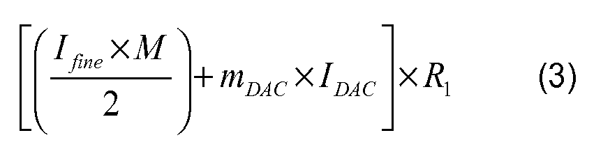
where mDAC is the number of DAC bits and IDAC is the tail current source of each DAC bit. - After this example, the importance of the slow steering DAC should become clear. Unless the steering of the DAC is not much slower than the (1/2πfHP), where fhp is set by the integrator stage and the fine transconductance stage, and it must be in the rage of 0.1 Hz - 1 Hz for most of the biomedical signal acquisition applications, then the steering of the DAC would create a voltage step at the output of the instrumentation amplifier. This is undesired since it can saturate the output of the instrumentation amplifier.
- The fHP is defined by:

where gm,fine is the transconductance of the input pair stage of the fine transconductance stage, M is the mirror ratio of the fine transconductance stage, Av,INT is the open loop gain of the on-chip integrator, A is the gain of the second gain stage connected to the output of the CBIA, and fLP,INT is the low-pass corner frequency of the on-chip integrator. The result of this equation for the current implementation is 0.1Hz. Since even the fastest steering time of the slow steering DAC is 300 seconds, which is much slower that (1/2πfHP), the fine transconductance stage can prevent the step response at the output. - The main advantage of using such fine-coarse architecture is the reduction of the current that is consumed in the fine transconductance stage. It should be noted that the current consumed in the input stage of the fine transconductance stage is wasted. On the other hand, the 16-bit slow steering current DAC actually supplies the bias current of the CBIA, therefore the increase in the DAC current also reduces the noise of the CBIA. If the figure of merit is defined by the following equation:

- In a preferred embodiment, this ACCIA is used as a front-end of a readout channel. The proposed circuit can for example be used in an EEG acquisition system. A complete EEG Acquisition ASIC can be designed (see
Figure 9 ), where the outputs of the analog readout front-ends can be digitized using the on-chip low-power ADC. This eliminates the use of an external ADC that not only improves the power dissipation of the EEG acquisition system but also can shrink the system size. -
Figure 9 shows the architecture of the proposed EEG acquisition ASIC. The main building blocks of the ASIC are: eight readout front-end channels, an 11-bit SAR ADC, a bias circuit, a 1 MHz relaxation oscillator, an electrode impedance measurement circuit, and a calibration signal generator. The readout front-end channels are responsible for extracting and conditioning the EEG signals from the biopotential electrodes. The preamplifier of a readout channel is the presented ACCIA. The ACCIA is followed by a chopping spike filter (CSF) stage, which includes a HPF with adjustable cut-off frequency. After the CSF stage a programmable gain stage further amplifies the extracted biopotential signals. The output of each channel is buffered and time-multiplexed. Finally, a class-AB buffer buffers the outputs of the channels and drives the input capacitance of the ADC. - The ADC of the ASIC is implemented using the SAR-ADC architecture due to its low-power dissipation characteristics. The operating clock of the ADC is generated by the on-chip 1MHz relaxation oscillator. The operation of the relaxation oscillator is duty cycled such that it generates the 1MHz clock only when the ADC is asked to convert an analog input signal. The reference voltage of the ADC is generated by the bias circuit, and it is buffered by a class-AB buffer to drive the capacitive DAC of the SAR-ADC.
- The ASIC is designed for battery powered systems, where the supply voltage changes as the battery discharges. Therefore, the bias generator circuit of the ASIC uses a PTAT voltage generator to generate a temperature and supply independent reference voltage. This reference voltage is used to generate all the bias voltages and currents of the ASIC, as well as the reference voltage of the ADC. Additionally, it should be noted that the patient bias voltage that is used for the grounding of the patient is also generated by the bias generator circuit.
- The digital control circuit of the ASIC uses a 32kHz clock input from which the sample signals of the analog multiplexer is generated, and to which the operation of the ADC is synchronized. The sample time of the first channel of the ASIC can be used as a synchronization signal with an external microcontroller. Additionally, the digital control circuit accepts a clock signal with 1ms pulse duration and 300s period. This clock is necessary for the operation of the coarse transconductance stage of the ACCIA. During this 1ms pulse time the coarse transconductance stage checks whether the fine transconductance stage has reached its limits. If so, the coarse transconductance stage adjusts its output accordingly. However, this slow operation of the coarse transconductance stage can make the start-up of the ACCIA circuit extremely slow. Therefore, the ASIC has a start-up mode.
- Finally, the ASIC includes an electrode impedance measurement and calibration modes, which enable the user to measure the impedances of the biopotential electrodes and to calibrate the matching of the readout front-end channels, respectively.
-
- [1] R. F. Yazicioglu, P. Merken, R. Puers, and C. Van Hoof, "60_µW 60nV/pHz readout front-end for portable biopotential acquisition systems," IEEE J. Solid-State Circuits, vol. 42, no. 5, pp. 1100-1110, May 2007.
- [2] T. Denison, K. Consoer, W. Santa, T. Avestruz, J. Cooley, and A. Kelly, "a 2µW 100nVh/√Hz Chopper-Stabilized Instrumentation Amplifier for Chronic Measurement of Neural Field Potentials," IEEE J. Solid-State Circuits, vol. 42, no. 12, Dec. 2007.
- [3] R. R. Harrison and C. Cameron, "A Low-Power Low-Noise CMOS Amplifier for Neural Recording Applications," IEEE J. Solid-State Circuits, vol. 38, no. 6, June 2003.
- [4] R. H. Olsson, M. N. Gulari, and K. D. Wise, "A Fully-Integrated Bandpass Amplifier for Extracellular Neural Recording," IEEE EMBS Conf. on Neural Eng., Italy, March 2003.
Claims (8)
- Large time constant steering circuit for slowly changing a voltage on a node between at least two discrete voltage levels, the circuit comprising an input node for receiving an input voltage, an output node for presenting an output voltage, a capacitive part connected at said output node for providing said output voltage and a resistive part connected between said input and output nodes for conducting a charging current from said input node to said capacitive part or a discharging current from said capacitive part to said input node depending on said input voltage, characterized in that said resistive part comprises a semiconductor structure connectable between said input node and said capacitive part in such a way that the semiconductor structure remains in an off state irrespective of the input and output voltages and passes only leakage currents for charging or discharging said capacitive part.
- Large time constant steering circuit according to claim 1, characterized in that said semiconductor structure comprises a first part in series with a second part, said first part being provided for remaining in said off state and passing said leakage current while charging and said second part being provided for remaining in said off state and passing said leakage current while discharging.
- Large time constant steering circuit according to claim 1 or 2, characterized in that said semiconductor structure comprises:a first transistor having a first conductive path in a first direction and a first gate for triggering said first conductive path,a second transistor having a second conductive path in a second direction and a second gate for triggering said second conductive path,said first and second conductive paths being connected in series between said input node and said capacitive part such that said first direction is opposite to said second direction,said first and second gates being connectable to a fixed voltage level for avoiding triggering of respectively said first and second conductive paths, thereby maintaining respectively said first and second transistors in said off state.
- Large time constant steering circuit according to claim 3, characterized in that said first and second transistors are provided on a common substrate.
- Large time constant steering circuit according to claim 3 or 4, characterized in that said first and second transistors are PMOS transistors with shorted source and bulk regions, said gates being jointly connectable to a supply voltage level.
- Large time constant steering circuit according to claim 3, 4 or 5, characterized in that said gates are further connectable to a ground level for fast steering purposes.
- Slow steering current DAC comprising a current source providing a current to a first branch and a second branch, characterized in that each branch comprises a pass gate connected to the output node of a large time constant steering circuit according to any one of the previous claims for controlling the current passing through each branch.
- Slow steering current DAC according to claim 7, characterized in that each branch further comprises a cascade transistor for increasing the output impedance of the current DAC.
Applications Claiming Priority (2)
| Application Number | Priority Date | Filing Date | Title |
|---|---|---|---|
| US2495408P | 2008-01-31 | 2008-01-31 | |
| EP08160365A EP2086111B1 (en) | 2008-01-31 | 2008-07-14 | Instrumentation amplifier |
Related Parent Applications (4)
| Application Number | Title | Priority Date | Filing Date |
|---|---|---|---|
| EP08160365.6 Division | 2008-07-14 | ||
| EP08160365 Previously-Filed-Application | 2008-07-14 | ||
| EP08160365A Division EP2086111B1 (en) | 2008-01-31 | 2008-07-14 | Instrumentation amplifier |
| EP08160365A Previously-Filed-Application EP2086111B1 (en) | 2008-01-31 | 2008-07-14 | Instrumentation amplifier |
Publications (2)
| Publication Number | Publication Date |
|---|---|
| EP2309644A1 true EP2309644A1 (en) | 2011-04-13 |
| EP2309644B1 EP2309644B1 (en) | 2015-09-02 |
Family
ID=40225457
Family Applications (2)
| Application Number | Title | Priority Date | Filing Date |
|---|---|---|---|
| EP08160365A Not-in-force EP2086111B1 (en) | 2008-01-31 | 2008-07-14 | Instrumentation amplifier |
| EP11151396.6A Not-in-force EP2309644B1 (en) | 2008-01-31 | 2008-07-14 | Large time constant steering circuit |
Family Applications Before (1)
| Application Number | Title | Priority Date | Filing Date |
|---|---|---|---|
| EP08160365A Not-in-force EP2086111B1 (en) | 2008-01-31 | 2008-07-14 | Instrumentation amplifier |
Country Status (4)
| Country | Link |
|---|---|
| US (2) | US7920005B2 (en) |
| EP (2) | EP2086111B1 (en) |
| AT (1) | ATE499744T1 (en) |
| DE (1) | DE602008005105D1 (en) |
Families Citing this family (17)
| Publication number | Priority date | Publication date | Assignee | Title |
|---|---|---|---|---|
| US7944251B2 (en) * | 2009-03-09 | 2011-05-17 | Broadcom Corporation | Reduced line driver output dependency on process, voltage, and temperature variations |
| EP2294978B1 (en) | 2009-09-14 | 2013-09-04 | Imec | Adaptive sampling of an electrocardiogram |
| EP2298164B1 (en) | 2009-09-14 | 2013-05-15 | Imec | Cardiac monitoring circuit with adaptive sampling |
| EP2294979B1 (en) | 2009-09-14 | 2013-12-18 | Imec | Method and electronic medical device for simultaneously measuring an impedance and a biopotential signal |
| TWI473424B (en) * | 2011-09-16 | 2015-02-11 | Univ Nat Central | Adjustable Voltage Control Virtual Resistance Architecture |
| WO2013123358A1 (en) * | 2012-02-17 | 2013-08-22 | Massachusetts Institute Of Technology | Multi-channel scalable eeg acquisition system on a chip with integrated patient specific seizure classification and recording processor |
| US9351653B1 (en) * | 2012-11-29 | 2016-05-31 | Intan Technologies, LLC | Multi-channel reconfigurable systems and methods for sensing biopotential signals |
| KR101937676B1 (en) | 2014-01-13 | 2019-01-14 | 삼성전자주식회사 | Bio signal amplifying circuit |
| US9379728B1 (en) * | 2015-06-26 | 2016-06-28 | Stmicroelectronics International N.V. | Self-calibrated digital-to-analog converter |
| TWI611659B (en) * | 2017-02-13 | 2018-01-11 | 華邦電子股份有限公司 | Pseudo resistor with tunable resistance |
| CN108429545B (en) * | 2017-02-13 | 2022-05-31 | 华邦电子股份有限公司 | Adjustable resistance type virtual resistor |
| US10574212B2 (en) * | 2017-11-21 | 2020-02-25 | Mediatek Inc. | Method and circuit for low-noise reference signal generation |
| CN109091115B (en) * | 2018-09-17 | 2023-08-08 | 电子科技大学 | Direct current suppression device applied to physiological signal acquisition |
| WO2020102305A1 (en) * | 2018-11-13 | 2020-05-22 | Rensselaer Polytechnic Institute | Reconfigurable analog front end for biosignal acquisition |
| WO2021034408A2 (en) | 2019-06-27 | 2021-02-25 | Hsu, Yu-Pin | System for sensing arterial pulse waveform |
| US11387811B2 (en) * | 2020-10-16 | 2022-07-12 | Semiconductor Components Industries, Llc | Noise filter |
| EP4479128B1 (en) * | 2022-02-17 | 2026-08-19 | Ecole Polytechnique Fédérale de Lausanne (EPFL) | A multichannel versatile brain activity classification and closed loop neuromodulation system, device and method using a highly multiplexed mixed-signal front-end |
Citations (2)
| Publication number | Priority date | Publication date | Assignee | Title |
|---|---|---|---|---|
| EP0849878A2 (en) * | 1996-12-19 | 1998-06-24 | Texas Instruments Incorporated | Improvements in or relating to integrated circuits |
| US6346851B1 (en) * | 1999-12-14 | 2002-02-12 | Texas Instruments Incorporated | Low-pass filter with improved high frequency attenuation |
Family Cites Families (9)
| Publication number | Priority date | Publication date | Assignee | Title |
|---|---|---|---|---|
| US3601676A (en) * | 1969-08-20 | 1971-08-24 | Information Storage Systems | Balance circuit for dc servos |
| US3646420A (en) * | 1969-08-20 | 1972-02-29 | Information Storage Systems | Balance circuit for dc servos |
| US5461322A (en) * | 1991-10-29 | 1995-10-24 | Geo-Centers, Inc. | Autonulling DC bridge for real-time sensor transduction and voltage measurements |
| US5793241A (en) * | 1995-11-30 | 1998-08-11 | Cherry Semiconductor Corporation | High speed active op-amp clamp |
| US5953690A (en) * | 1996-07-01 | 1999-09-14 | Pacific Fiberoptics, Inc. | Intelligent fiberoptic receivers and method of operating and manufacturing the same |
| US6262625B1 (en) * | 1999-10-29 | 2001-07-17 | Hewlett-Packard Co | Operational amplifier with digital offset calibration |
| US6621343B2 (en) * | 2001-08-07 | 2003-09-16 | Infineon Technologies Ag | Open loop variable gain amplifier using replica gain cell |
| WO2005022194A2 (en) * | 2003-08-13 | 2005-03-10 | Lettvin Jonathan D | Imaging system |
| US7795960B2 (en) * | 2007-09-14 | 2010-09-14 | Analog Devices, Inc. | Low power, low noise amplifier system |
-
2008
- 2008-07-14 EP EP08160365A patent/EP2086111B1/en not_active Not-in-force
- 2008-07-14 AT AT08160365T patent/ATE499744T1/en not_active IP Right Cessation
- 2008-07-14 EP EP11151396.6A patent/EP2309644B1/en not_active Not-in-force
- 2008-07-14 DE DE602008005105T patent/DE602008005105D1/en active Active
-
2009
- 2009-01-30 US US12/362,687 patent/US7920005B2/en not_active Expired - Fee Related
-
2011
- 2011-02-25 US US13/035,210 patent/US8466742B2/en not_active Expired - Fee Related
Patent Citations (2)
| Publication number | Priority date | Publication date | Assignee | Title |
|---|---|---|---|---|
| EP0849878A2 (en) * | 1996-12-19 | 1998-06-24 | Texas Instruments Incorporated | Improvements in or relating to integrated circuits |
| US6346851B1 (en) * | 1999-12-14 | 2002-02-12 | Texas Instruments Incorporated | Low-pass filter with improved high frequency attenuation |
Also Published As
| Publication number | Publication date |
|---|---|
| EP2086111A3 (en) | 2010-01-13 |
| EP2086111B1 (en) | 2011-02-23 |
| US7920005B2 (en) | 2011-04-05 |
| ATE499744T1 (en) | 2011-03-15 |
| US20110193623A1 (en) | 2011-08-11 |
| DE602008005105D1 (en) | 2011-04-07 |
| US8466742B2 (en) | 2013-06-18 |
| US20090195319A1 (en) | 2009-08-06 |
| EP2086111A2 (en) | 2009-08-05 |
| EP2309644B1 (en) | 2015-09-02 |
Similar Documents
| Publication | Publication Date | Title |
|---|---|---|
| EP2086111B1 (en) | Instrumentation amplifier | |
| Wu et al. | 1.2 V CMOS switched-capacitor circuits | |
| US20130169361A1 (en) | Multi-Stage Fully Differential Amplifier with Controlled Common Mode Voltage | |
| JP2019194855A (en) | Power-cycling of voltage reference | |
| EP2295944A2 (en) | Temperature sensor | |
| US20110241780A1 (en) | Amplifier circuit, signal processor circuit, and semiconductor integrated circuit device | |
| Das et al. | A novel low-noise fully differential CMOS instrumentation amplifier with 1.88 noise efficiency factor for biomedical and sensor applications | |
| CN106877830B (en) | Analog front-end circuit for detecting physiological potential signals | |
| US20220206100A1 (en) | Pseudo-resistance calibration circuit based on switched capacitor | |
| Horestani et al. | Ultra-high-resistance pseudo-resistors with small variations in a wide symmetrical input voltage swing | |
| Kim et al. | An ultra low-power low-noise neural recording analog front-end IC for implantable devices | |
| US7696791B2 (en) | High-speed amplitude detector with a digital output | |
| Abhilash et al. | A high gain, high CMRR two-stage fully differential amplifier using g m/I d technique for bio-medical applications | |
| Moulahcene et al. | A low power low noise chopper-stabilized two-stage operational amplifier for portable bio-potential acquisition systems using 90 nm technology | |
| Nolan | Demystifying Auto-Zero Amplifiers—Part | |
| Arnaud et al. | A fully integrated 0.5-7 Hz CMOS bandpass amplifier | |
| US6778005B2 (en) | High PSRR current source | |
| Taha et al. | Design of a low noise single-ended sensor interface amplifier for bio-potential applications | |
| Udupa et al. | ECG analog front-end in 180 nm CMOS technology | |
| Siemssen et al. | A Trimming-Free 3-in-1 Multi-Mode Passive Switched-Capacitor Amplifier With an Absolute Logarithmic Error of 0.5 dB up to 200° C | |
| JP2004064262A (en) | Differential amplifier circuit and reception circuit for radio controlled watch | |
| Chen et al. | A low noise CMOS charge sensitive preamplifier for MEMS capacitive accelerometer readout | |
| Diño et al. | High CMRR and Low Output Offset Current Mode Instrumentation Amplifier for Wearable Ballistocardiography Application | |
| Lee et al. | A 0.9 V rail-to-rail constant g/sub m/amplifier for implantable biomedical applications | |
| US7423460B2 (en) | Sine wave shaper with very low total harmonic distortion |
Legal Events
| Date | Code | Title | Description |
|---|---|---|---|
| PUAI | Public reference made under article 153(3) epc to a published international application that has entered the european phase |
Free format text: ORIGINAL CODE: 0009012 |
|
| AC | Divisional application: reference to earlier application |
Ref document number: 2086111 Country of ref document: EP Kind code of ref document: P |
|
| AK | Designated contracting states |
Kind code of ref document: A1 Designated state(s): AT BE BG CH CY CZ DE DK EE ES FI FR GB GR HR HU IE IS IT LI LT LU LV MC MT NL NO PL PT RO SE SI SK TR |
|
| RIN1 | Information on inventor provided before grant (corrected) |
Inventor name: MERKEN, PATRICK Inventor name: YAZICIOGLU, REFET FIRAT |
|
| RIN1 | Information on inventor provided before grant (corrected) |
Inventor name: MERKEN, PATRICK Inventor name: YAZICIOGLU, REFET FIRAT |
|
| 17P | Request for examination filed |
Effective date: 20111012 |
|
| 17Q | First examination report despatched |
Effective date: 20111102 |
|
| REG | Reference to a national code |
Ref country code: DE Ref legal event code: R079 Ref document number: 602008040012 Country of ref document: DE Free format text: PREVIOUS MAIN CLASS: H03H0001020000 Ipc: H03F0003387000 |
|
| GRAP | Despatch of communication of intention to grant a patent |
Free format text: ORIGINAL CODE: EPIDOSNIGR1 |
|
| RIC1 | Information provided on ipc code assigned before grant |
Ipc: H03F 3/387 20060101AFI20150224BHEP Ipc: H03F 3/45 20060101ALI20150224BHEP Ipc: A61B 5/0428 20060101ALI20150224BHEP Ipc: H03K 17/16 20060101ALI20150224BHEP Ipc: H03H 11/04 20060101ALI20150224BHEP Ipc: H03H 1/02 20060101ALI20150224BHEP Ipc: A61B 5/0476 20060101ALN20150224BHEP |
|
| INTG | Intention to grant announced |
Effective date: 20150310 |
|
| GRAS | Grant fee paid |
Free format text: ORIGINAL CODE: EPIDOSNIGR3 |
|
| RAP1 | Party data changed (applicant data changed or rights of an application transferred) |
Owner name: KATHOLIEKE UNIVERSITEIT LEUVEN Owner name: IMEC |
|
| GRAA | (expected) grant |
Free format text: ORIGINAL CODE: 0009210 |
|
| AC | Divisional application: reference to earlier application |
Ref document number: 2086111 Country of ref document: EP Kind code of ref document: P |
|
| AK | Designated contracting states |
Kind code of ref document: B1 Designated state(s): AT BE BG CH CY CZ DE DK EE ES FI FR GB GR HR HU IE IS IT LI LT LU LV MC MT NL NO PL PT RO SE SI SK TR |
|
| REG | Reference to a national code |
Ref country code: GB Ref legal event code: FG4D |
|
| REG | Reference to a national code |
Ref country code: AT Ref legal event code: REF Ref document number: 747158 Country of ref document: AT Kind code of ref document: T Effective date: 20150915 Ref country code: CH Ref legal event code: EP |
|
| REG | Reference to a national code |
Ref country code: IE Ref legal event code: FG4D |
|
| REG | Reference to a national code |
Ref country code: DE Ref legal event code: R096 Ref document number: 602008040012 Country of ref document: DE |
|
| REG | Reference to a national code |
Ref country code: AT Ref legal event code: MK05 Ref document number: 747158 Country of ref document: AT Kind code of ref document: T Effective date: 20150902 |
|
| PG25 | Lapsed in a contracting state [announced via postgrant information from national office to epo] |
Ref country code: NO Free format text: LAPSE BECAUSE OF FAILURE TO SUBMIT A TRANSLATION OF THE DESCRIPTION OR TO PAY THE FEE WITHIN THE PRESCRIBED TIME-LIMIT Effective date: 20151202 Ref country code: LV Free format text: LAPSE BECAUSE OF FAILURE TO SUBMIT A TRANSLATION OF THE DESCRIPTION OR TO PAY THE FEE WITHIN THE PRESCRIBED TIME-LIMIT Effective date: 20150902 Ref country code: GR Free format text: LAPSE BECAUSE OF FAILURE TO SUBMIT A TRANSLATION OF THE DESCRIPTION OR TO PAY THE FEE WITHIN THE PRESCRIBED TIME-LIMIT Effective date: 20151203 Ref country code: FI Free format text: LAPSE BECAUSE OF FAILURE TO SUBMIT A TRANSLATION OF THE DESCRIPTION OR TO PAY THE FEE WITHIN THE PRESCRIBED TIME-LIMIT Effective date: 20150902 Ref country code: LT Free format text: LAPSE BECAUSE OF FAILURE TO SUBMIT A TRANSLATION OF THE DESCRIPTION OR TO PAY THE FEE WITHIN THE PRESCRIBED TIME-LIMIT Effective date: 20150902 |
|
| REG | Reference to a national code |
Ref country code: LT Ref legal event code: MG4D Ref country code: NL Ref legal event code: MP Effective date: 20150902 |
|
| PG25 | Lapsed in a contracting state [announced via postgrant information from national office to epo] |
Ref country code: PL Free format text: LAPSE BECAUSE OF FAILURE TO SUBMIT A TRANSLATION OF THE DESCRIPTION OR TO PAY THE FEE WITHIN THE PRESCRIBED TIME-LIMIT Effective date: 20150902 Ref country code: ES Free format text: LAPSE BECAUSE OF FAILURE TO SUBMIT A TRANSLATION OF THE DESCRIPTION OR TO PAY THE FEE WITHIN THE PRESCRIBED TIME-LIMIT Effective date: 20150902 Ref country code: AT Free format text: LAPSE BECAUSE OF FAILURE TO SUBMIT A TRANSLATION OF THE DESCRIPTION OR TO PAY THE FEE WITHIN THE PRESCRIBED TIME-LIMIT Effective date: 20150902 Ref country code: SE Free format text: LAPSE BECAUSE OF FAILURE TO SUBMIT A TRANSLATION OF THE DESCRIPTION OR TO PAY THE FEE WITHIN THE PRESCRIBED TIME-LIMIT Effective date: 20150902 |
|
| PG25 | Lapsed in a contracting state [announced via postgrant information from national office to epo] |
Ref country code: EE Free format text: LAPSE BECAUSE OF FAILURE TO SUBMIT A TRANSLATION OF THE DESCRIPTION OR TO PAY THE FEE WITHIN THE PRESCRIBED TIME-LIMIT Effective date: 20150902 Ref country code: SK Free format text: LAPSE BECAUSE OF FAILURE TO SUBMIT A TRANSLATION OF THE DESCRIPTION OR TO PAY THE FEE WITHIN THE PRESCRIBED TIME-LIMIT Effective date: 20150902 Ref country code: IS Free format text: LAPSE BECAUSE OF FAILURE TO SUBMIT A TRANSLATION OF THE DESCRIPTION OR TO PAY THE FEE WITHIN THE PRESCRIBED TIME-LIMIT Effective date: 20160102 Ref country code: NL Free format text: LAPSE BECAUSE OF FAILURE TO SUBMIT A TRANSLATION OF THE DESCRIPTION OR TO PAY THE FEE WITHIN THE PRESCRIBED TIME-LIMIT Effective date: 20150902 Ref country code: IT Free format text: LAPSE BECAUSE OF FAILURE TO SUBMIT A TRANSLATION OF THE DESCRIPTION OR TO PAY THE FEE WITHIN THE PRESCRIBED TIME-LIMIT Effective date: 20150902 Ref country code: CZ Free format text: LAPSE BECAUSE OF FAILURE TO SUBMIT A TRANSLATION OF THE DESCRIPTION OR TO PAY THE FEE WITHIN THE PRESCRIBED TIME-LIMIT Effective date: 20150902 |
|
| PG25 | Lapsed in a contracting state [announced via postgrant information from national office to epo] |
Ref country code: RO Free format text: LAPSE BECAUSE OF FAILURE TO SUBMIT A TRANSLATION OF THE DESCRIPTION OR TO PAY THE FEE WITHIN THE PRESCRIBED TIME-LIMIT Effective date: 20150902 Ref country code: PT Free format text: LAPSE BECAUSE OF FAILURE TO SUBMIT A TRANSLATION OF THE DESCRIPTION OR TO PAY THE FEE WITHIN THE PRESCRIBED TIME-LIMIT Effective date: 20160104 |
|
| REG | Reference to a national code |
Ref country code: DE Ref legal event code: R097 Ref document number: 602008040012 Country of ref document: DE |
|
| REG | Reference to a national code |
Ref country code: FR Ref legal event code: PLFP Year of fee payment: 9 |
|
| PLBE | No opposition filed within time limit |
Free format text: ORIGINAL CODE: 0009261 |
|
| STAA | Information on the status of an ep patent application or granted ep patent |
Free format text: STATUS: NO OPPOSITION FILED WITHIN TIME LIMIT |
|
| 26N | No opposition filed |
Effective date: 20160603 |
|
| PG25 | Lapsed in a contracting state [announced via postgrant information from national office to epo] |
Ref country code: SI Free format text: LAPSE BECAUSE OF FAILURE TO SUBMIT A TRANSLATION OF THE DESCRIPTION OR TO PAY THE FEE WITHIN THE PRESCRIBED TIME-LIMIT Effective date: 20150902 Ref country code: DK Free format text: LAPSE BECAUSE OF FAILURE TO SUBMIT A TRANSLATION OF THE DESCRIPTION OR TO PAY THE FEE WITHIN THE PRESCRIBED TIME-LIMIT Effective date: 20150902 |
|
| PG25 | Lapsed in a contracting state [announced via postgrant information from national office to epo] |
Ref country code: BE Free format text: LAPSE BECAUSE OF FAILURE TO SUBMIT A TRANSLATION OF THE DESCRIPTION OR TO PAY THE FEE WITHIN THE PRESCRIBED TIME-LIMIT Effective date: 20150902 |
|
| REG | Reference to a national code |
Ref country code: CH Ref legal event code: PL |
|
| PG25 | Lapsed in a contracting state [announced via postgrant information from national office to epo] |
Ref country code: MC Free format text: LAPSE BECAUSE OF FAILURE TO SUBMIT A TRANSLATION OF THE DESCRIPTION OR TO PAY THE FEE WITHIN THE PRESCRIBED TIME-LIMIT Effective date: 20150902 |
|
| PG25 | Lapsed in a contracting state [announced via postgrant information from national office to epo] |
Ref country code: CH Free format text: LAPSE BECAUSE OF NON-PAYMENT OF DUE FEES Effective date: 20160731 Ref country code: LI Free format text: LAPSE BECAUSE OF NON-PAYMENT OF DUE FEES Effective date: 20160731 |
|
| REG | Reference to a national code |
Ref country code: IE Ref legal event code: MM4A |
|
| REG | Reference to a national code |
Ref country code: FR Ref legal event code: PLFP Year of fee payment: 10 |
|
| PG25 | Lapsed in a contracting state [announced via postgrant information from national office to epo] |
Ref country code: IE Free format text: LAPSE BECAUSE OF NON-PAYMENT OF DUE FEES Effective date: 20160714 |
|
| PG25 | Lapsed in a contracting state [announced via postgrant information from national office to epo] |
Ref country code: LU Free format text: LAPSE BECAUSE OF NON-PAYMENT OF DUE FEES Effective date: 20160714 |
|
| PG25 | Lapsed in a contracting state [announced via postgrant information from national office to epo] |
Ref country code: CY Free format text: LAPSE BECAUSE OF FAILURE TO SUBMIT A TRANSLATION OF THE DESCRIPTION OR TO PAY THE FEE WITHIN THE PRESCRIBED TIME-LIMIT Effective date: 20150902 Ref country code: HU Free format text: LAPSE BECAUSE OF FAILURE TO SUBMIT A TRANSLATION OF THE DESCRIPTION OR TO PAY THE FEE WITHIN THE PRESCRIBED TIME-LIMIT; INVALID AB INITIO Effective date: 20080714 |
|
| REG | Reference to a national code |
Ref country code: FR Ref legal event code: PLFP Year of fee payment: 11 |
|
| PG25 | Lapsed in a contracting state [announced via postgrant information from national office to epo] |
Ref country code: HR Free format text: LAPSE BECAUSE OF FAILURE TO SUBMIT A TRANSLATION OF THE DESCRIPTION OR TO PAY THE FEE WITHIN THE PRESCRIBED TIME-LIMIT Effective date: 20150902 Ref country code: MT Free format text: LAPSE BECAUSE OF NON-PAYMENT OF DUE FEES Effective date: 20160731 Ref country code: TR Free format text: LAPSE BECAUSE OF FAILURE TO SUBMIT A TRANSLATION OF THE DESCRIPTION OR TO PAY THE FEE WITHIN THE PRESCRIBED TIME-LIMIT Effective date: 20150902 |
|
| PG25 | Lapsed in a contracting state [announced via postgrant information from national office to epo] |
Ref country code: BG Free format text: LAPSE BECAUSE OF FAILURE TO SUBMIT A TRANSLATION OF THE DESCRIPTION OR TO PAY THE FEE WITHIN THE PRESCRIBED TIME-LIMIT Effective date: 20150902 |
|
| PGFP | Annual fee paid to national office [announced via postgrant information from national office to epo] |
Ref country code: FR Payment date: 20210623 Year of fee payment: 14 |
|
| PGFP | Annual fee paid to national office [announced via postgrant information from national office to epo] |
Ref country code: GB Payment date: 20210623 Year of fee payment: 14 |
|
| PGFP | Annual fee paid to national office [announced via postgrant information from national office to epo] |
Ref country code: DE Payment date: 20210622 Year of fee payment: 14 |
|
| REG | Reference to a national code |
Ref country code: DE Ref legal event code: R119 Ref document number: 602008040012 Country of ref document: DE |
|
| GBPC | Gb: european patent ceased through non-payment of renewal fee |
Effective date: 20220714 |
|
| PG25 | Lapsed in a contracting state [announced via postgrant information from national office to epo] |
Ref country code: FR Free format text: LAPSE BECAUSE OF NON-PAYMENT OF DUE FEES Effective date: 20220731 |
|
| PG25 | Lapsed in a contracting state [announced via postgrant information from national office to epo] |
Ref country code: GB Free format text: LAPSE BECAUSE OF NON-PAYMENT OF DUE FEES Effective date: 20220714 Ref country code: DE Free format text: LAPSE BECAUSE OF NON-PAYMENT OF DUE FEES Effective date: 20230201 |