EP2309543A1 - Method for enhancing the reliability of a P-channel semiconductor device and a P-channel semiconductor device made thereof - Google Patents
Method for enhancing the reliability of a P-channel semiconductor device and a P-channel semiconductor device made thereof Download PDFInfo
- Publication number
- EP2309543A1 EP2309543A1 EP10186985A EP10186985A EP2309543A1 EP 2309543 A1 EP2309543 A1 EP 2309543A1 EP 10186985 A EP10186985 A EP 10186985A EP 10186985 A EP10186985 A EP 10186985A EP 2309543 A1 EP2309543 A1 EP 2309543A1
- Authority
- EP
- European Patent Office
- Prior art keywords
- layer
- channel
- semiconductor
- semiconductor device
- bandgap
- Prior art date
- Legal status (The legal status is an assumption and is not a legal conclusion. Google has not performed a legal analysis and makes no representation as to the accuracy of the status listed.)
- Granted
Links
Images




Classifications
-
- H—ELECTRICITY
- H10—SEMICONDUCTOR DEVICES; ELECTRIC SOLID-STATE DEVICES NOT OTHERWISE PROVIDED FOR
- H10D—INORGANIC ELECTRIC SEMICONDUCTOR DEVICES
- H10D30/00—Field-effect transistors [FET]
- H10D30/60—Insulated-gate field-effect transistors [IGFET]
- H10D30/751—Insulated-gate field-effect transistors [IGFET] having composition variations in the channel regions
-
- H—ELECTRICITY
- H10—SEMICONDUCTOR DEVICES; ELECTRIC SOLID-STATE DEVICES NOT OTHERWISE PROVIDED FOR
- H10D—INORGANIC ELECTRIC SEMICONDUCTOR DEVICES
- H10D64/00—Electrodes of devices having potential barriers
- H10D64/60—Electrodes characterised by their materials
- H10D64/66—Electrodes having a conductor capacitively coupled to a semiconductor by an insulator, e.g. MIS electrodes
- H10D64/68—Electrodes having a conductor capacitively coupled to a semiconductor by an insulator, e.g. MIS electrodes characterised by the insulator, e.g. by the gate insulator
- H10D64/691—Electrodes having a conductor capacitively coupled to a semiconductor by an insulator, e.g. MIS electrodes characterised by the insulator, e.g. by the gate insulator comprising metallic compounds, e.g. metal oxides or metal silicates
-
- H—ELECTRICITY
- H10—SEMICONDUCTOR DEVICES; ELECTRIC SOLID-STATE DEVICES NOT OTHERWISE PROVIDED FOR
- H10D—INORGANIC ELECTRIC SEMICONDUCTOR DEVICES
- H10D30/00—Field-effect transistors [FET]
- H10D30/60—Insulated-gate field-effect transistors [IGFET]
- H10D30/791—Arrangements for exerting mechanical stress on the crystal lattice of the channel regions
- H10D30/798—Arrangements for exerting mechanical stress on the crystal lattice of the channel regions being provided in or under the channel regions
-
- H—ELECTRICITY
- H10—SEMICONDUCTOR DEVICES; ELECTRIC SOLID-STATE DEVICES NOT OTHERWISE PROVIDED FOR
- H10D—INORGANIC ELECTRIC SEMICONDUCTOR DEVICES
- H10D64/00—Electrodes of devices having potential barriers
- H10D64/60—Electrodes characterised by their materials
- H10D64/66—Electrodes having a conductor capacitively coupled to a semiconductor by an insulator, e.g. MIS electrodes
- H10D64/667—Electrodes having a conductor capacitively coupled to a semiconductor by an insulator, e.g. MIS electrodes the conductor comprising a layer of alloy material, compound material or organic material contacting the insulator, e.g. TiN workfunction layers
-
- H—ELECTRICITY
- H10—SEMICONDUCTOR DEVICES; ELECTRIC SOLID-STATE DEVICES NOT OTHERWISE PROVIDED FOR
- H10D—INORGANIC ELECTRIC SEMICONDUCTOR DEVICES
- H10D64/00—Electrodes of devices having potential barriers
- H10D64/60—Electrodes characterised by their materials
- H10D64/66—Electrodes having a conductor capacitively coupled to a semiconductor by an insulator, e.g. MIS electrodes
- H10D64/68—Electrodes having a conductor capacitively coupled to a semiconductor by an insulator, e.g. MIS electrodes characterised by the insulator, e.g. by the gate insulator
- H10D64/681—Electrodes having a conductor capacitively coupled to a semiconductor by an insulator, e.g. MIS electrodes characterised by the insulator, e.g. by the gate insulator having a compositional variation, e.g. multilayered
- H10D64/685—Electrodes having a conductor capacitively coupled to a semiconductor by an insulator, e.g. MIS electrodes characterised by the insulator, e.g. by the gate insulator having a compositional variation, e.g. multilayered being perpendicular to the channel plane
Definitions
- the present invention relates to the field of semiconductor devices, more particularly to the field of P-channel semiconductor devices.
- the present invention relates to enhancing reliability, more particularly NBTI reliability, of such devices.
- Embodiments of the present invention are particularly useful for sub-1 nm EOT devices.
- Negative bias temperature instability is a significant reliability concern for submicron CMOS technologies, particularly to the PMOS transistors therein. It is widely believed that NBTI degradation is due to generation of interface traps, which are unsaturated silicon dangling bonds.
- One of the most popular models explaining NBTI phenomenon is the reaction diffusion model. This model proposes that the generation of interface traps is because of a hole induced electrochemical reaction at the Si-SiO 2 interface. In the initial times the degradation is reaction rate controlled, however, with time the phenomenon becomes diffusion limited. In addition to this, it is also believed that a consistent part of the NBTI degradation is due to a hole-trapping mechanism, whereby a hole gets trapped in a trap state, causing a shift in the threshold voltage.
- NBTI has always been associated with the CMOS development, but it was not considered of great importance because of the low electric fields in operation. However, as there is an increasing demand for higher drive current, NBTI has become a major reliability problem for the semiconductor industry, in particular it is a key reliability issue in MOSFETs.
- NBTI When a P-channel semiconductor device, such as a PMOSFET, is biased with negative gate voltages especially at elevated temperatures, i.e. normal operating conditions, degradation of main device parameters (threshold voltage, transconductance, drive current, subthreshold slope, etc.) is observed: NBTI manifests as an increase in the threshold voltage and a consequent decrease in drain current and transconductance. The mechanism is caused by holes interacting with defect precursors in the oxide and at the oxide/semiconductor interface.
- EOT effective oxide thickness
- E ox oxide electric field
- the present invention provides a method for forming a P-channel semiconductor device with good NBTI reliability.
- the method comprises providing a P-channel semiconductor device comprising a P-channel layer, and a control electrode on the semiconductor P-channel layer comprising at least a gate dielectric layer.
- the gate dielectric layer has a conduction band and a valence band, there being an energy bandgap between the conduction band and the valence band.
- the gate dielectric layer has an exponentially-shaped distribution of defect levels E(defect) in its energy bandgap, the exponentially-shaped distribution of defect levels having a lower concentration of defect levels at the centre of the bandgap and a higher concentration of defect levels at the edges of the bandgap.
- the density of defect levels in the gate dielectric layer is exponentially decreasing as a function of energy from the band edges of an adjacent layer.
- the adjacent layer considered is the one adjacent to the gate dielectric layer at a same side of the gate dielectric layer as the P-channel layer.
- the exponentially decreasing distribution of defect levels may be expressed as function of the energy of the band edges of the semiconductor P-channel layer itself.
- the exponentially decreasing distribution of defect levels may be expressed as a function of the energy of the band edges of a capping layer between the P-channel layer and the gate dielectric layer.
- the method according to embodiments of the present invention comprises selecting at least one parameter of the P-channel semiconductor device such that the inversion carrier injection into the distribution of defect levels occurs as close as possible to the centre of the bandgap of a layer adjacent the gate dielectric layer at the side of the P-channel layer, i.e. so that the inversion carrier injection level does deviate from the energy level at the centre of the bandgap of the adjacent layer with a value not more than 49%, such as not more than 40%, for example not more than 20%, not more than 10%, even not more than 5% of that bandgap (in eV).
- the layer adjacent the gate dielectric layer at the side of the P-channel layer may be the P-channel layer itself, or optionally a capping layer.
- selecting at least one parameter of the P-channel semiconductor device such that the inversion carrier injection level does deviate from the energy level at the centre of the bandgap of the adjacent layer with a value not more than 49%, such as not more than 40%, for example not more than 20%, not more than 10%, even not more than 5% of that bandgap (in eV) may comprise selecting the thickness of the semiconductor P-channel layer between a few mono-layers and 20 nm, for example between 3 nm and 20 nm, for example between 5 nm and 20 nm, such as between 7 nm and 20 nm.
- selecting parameters of the P-channel semiconductor device such that the inversion carrier injection level does deviate from the energy level at the centre of the bandgap of the adjacent layer with a value not more than 49%, such as not more than 40%, for example not more than 20%, not more than 10%, even not more than 5% of that bandgap (in eV) may comprise selecting the concentration in the semiconductor P-channel layer of the semiconductive element with the smallest bandgap between 25% and 99%.
- a method according to the present invention may comprise selecting the concentration in the semiconductor P-channel layer of the semiconductive element with the smallest bandgap higher than 50%, for example higher than 55%, e.g. higher than 60%.
- selecting parameters of the P-channel semiconductor device such that the inversion carrier injection level does deviate from the energy level at the centre of the bandgap of the adjacent layer with a value not more than 49%, such as not more than 40%, for example not more than 20%, not more than 10%, even not more than 5% of that bandgap (in eV) may comprise selecting the thickness of the semiconductor capping layer between 0.1 nm and 5 nm.
- a method according to the present invention may comprise selecting the thickness of the semiconductor capping layer 2 nm or below, for example 1.5 nm or below, 1 nm or below, 0.65 nm or below.
- a method according to embodiments of the present invention comprises selecting at least one parameter of the P-channel semiconductor device so as to obtain, compared to prior art methods, increased thickness of the P-channel layer, e.g. SiGe layer, and/or increased content of the smallest bandgap semiconductive element in the P-channel layer, e.g. increased Ge content in a SiGe layer, and/or decreased thickness of a capping layer, e.g. Si capping layer.
- a decreased thickness of a capping layer which is only optionally present, per se already yields good results in terms of NBTI reliability.
- the present invention provides a P-channel semiconductor device comprising a semiconductor P-channel layer, and a control electrode on the semiconductor P-channel layer.
- the control electrode comprises at least a gate dielectric layer, the gate dielectric layer having an exponentially-shaped distribution of defect levels E(defect) in its energy bandgap, the exponentially-shaped distribution of defect levels having a lower concentration of defect levels at the centre of the bandgap and a higher concentration of defect levels at the edges of the bandgap.
- the density of defect levels in the gate dielectric layer is exponentially decreasing as a function of energy from the band edges of an adjacent layer.
- the adjacent layer may be the semiconductor P-channel layer itself, or alternatively the adjacent layer may be a capping layer provided between the semiconductor P-channel layer and the gate dielectric layer.
- the P-channel semiconductor device has an inversion carrier injection into the distribution of defect levels which does deviate from the energy level at the centre of the bandgap of the adjacent layer with a value not more than 49%, such as not more than 40%, for example not more than 20%, not more than 10%, even not more than 5% of that bandgap (in eV).
- the P-channel layer comprises a combination of at least two semiconductive elements.
- the P-channel layer may be a SiGe layer.
- the thickness of the semiconductor P-channel layer e.g. the thickness of the SiGe layer, is between a few mono-layers and 20 nm, preferably higher than 3 nm, for example between 3 nm and 20 nm, for example between 5 nm and 20 nm, such as between 7 nm and 20 nm.
- the concentration in the semiconductor P-channel layer of the semiconductive element with the smallest bandgap may be between 25% and 99%, for example higher than 50%, for example higher than 55%, e.g. higher than 60%.
- the P-channel semiconductor device may comprise a capping layer between the semiconductor P-channel layer and the gate dielectric layer, and the thickness of the capping layer may be 2 nm or below, for example 1.5 nm or below, 1 nm or below, 0.65 nm or below.
- a P-channel semiconductor device may have a sub-1 nm EOT.
- One way to improve FET performance is by using a strained Si channel layer which incorporates Ge.
- the NBTI reliability of, in particular, such SiGe devices is described. This is, however, intended to be an example only, and is not intended to be limiting for the invention.
- the semiconductor device 10 also called herein a P-channel semiconductor device, illustrated in FIG. 1 comprises a substrate 11, e.g. Si substrate, with a semiconductor P-channel layer 12 thereon, e.g. a SiGe P-channel layer.
- the semiconductor P-channel layer has a valence band energy level E v (channel).
- the P-channel semiconductor device 10 furthermore comprises a gate dielectric layer 14, e.g. a SiO 2 layer, on the semiconductor P-channel layer 12.
- the gate dielectric layer 14 has a valence band energy level Agate dielectric).
- the density of defect levels E t in the gate dielectric layer 14 as function of energy is assumed to be exponentially decreasing from the band edges of the adjacent layer (being the semiconductor P-channel layer 12 or optionally, if present, a capping layer 13 between the P-channel layer 12 and the gate dielectric layer 14) toward the centre of the bandgap of this adjacent layer.
- the channel-dielectric band offset ⁇ E v towards a particular defect level at which charge carriers are injected from the channel into the dielectric is defined as E v (channel) - E t .
- the semiconductor device 10 may furthermore optionally comprise a capping layer 13, e.g. a Si cap, between the P-channel layer 12 and the gate dielectric layer 14 for having a good passivation of the interface, which is advantageous for device performance, a high-k dielectric layer 15, e.g. a HfO 2 dielectric layer, and a metal gate 16.
- the corresponding energy band diagram is illustrated in FIG. 2 for an exemplary semiconductor device according to embodiments comprising a SiGe p-channel layer, a Si capping layer and a gate stack comprising a metal gate (MG), a SiO 2 dielectric layer and HfO 2 dielectric layer.
- MG metal gate
- SiO 2 dielectric layer a SiO 2 dielectric layer
- HfO 2 dielectric layer a metal gate
- the semiconductor device 10 is by purpose engineered such that the inversion carrier injection into the distribution of defect levels occurs as close as possible to the centre of the bandgap of a layer adjacent the gate dielectric layer at the side of the P-channel layer(the semiconductor P-channel layer 12 itself or optionally the capping layer 13).
- the inversion carrier injection level does deviate from the energy level at the centre of the bandgap of the adjacent layer (the semiconductor P-channel layer 12 or optionally the capping layer 13) with a value not more than 49%, such as not more than 40%, for example not more than 20%, not more than 10%, even not more than 5% of that bandgap (in eV).
- the gate dielectric defect energy level is actually decoupled from the majority carriers in the channel, which are holes as the channel under consideration is of P-type, because of the low concentration of defects at that energy level.
- parameters of the semiconductor device 10 are selected such that holes from the semiconductor P-channel layer are prevented from interacting with the gate dielectric defect energy level. This may be obtained by engineering the semiconductor device such that the inversion carrier injection into the distribution of defect levels is so as to avoid interaction between carriers and a high concentration in the distribution of defect levels. This allows reducing NBTI (holes do not "see" the defect level).
- semiconductor devices for example SiGe semiconductor devices, provides a solution to the NBTI problem, in particular also for sub-1 nm EOT devices, thus significantly increasing operating overdrive voltages while still guaranteeing 10 year device lifetime.
- selecting parameters of the P-channel semiconductor device such that the inversion carrier injection into the distribution of defect levels does deviate from the energy level at the centre of the bandgap of the adjacent layer with a value not more than 49%, such as not more than 40%, for example not more than 20%, not more than 10%, even not more than 5% of that bandgap (in eV) comprises increasing the thickness of the semiconductor P-channel layer 12.
- the energy band diagrams of this embodiment are illustrated in FIG. 3 .
- the left hand side of FIG.3 illustrates the energy band diagram of a standard SiGe semiconductor device, having a thinner semiconductor P-channel layer 12, while the right hand side of FIG.
- FIG. 3 illustrates the energy band diagram of a gate stack in accordance with embodiments of the present invention, where the thickness of the semiconductor P-channel layer 12 is increased.
- Suitable thicknesses of the semiconductor P-channel layer 12, in case the semiconductor P-channel layer is a SiGe layer, are between a few mono-layers and about 20 nm. This upper limit corresponds to the critical thickness for which the SiGe layer relaxes and loses its compressive strain.
- the defect level distribution responsible for NBTI is indicated by 30.
- This defect level distribution 30 corresponds to energy levels and corresponding defect concentrations for a specific example of a SiGe P-FET device.
- the energy bands of the gate dielectric layer 14, indicated by 32 in FIG. 3 correspond to a specific example of a SiO 2 gate dielectric layer with a valence band energy level E v (gate dielectric) of a particular example of a SiGe P-FET device.
- FIG. 4 shows graphs setting out lifetime of devices in function of
- Graphs are set out for three different SiGe semiconductor devices: a first device with a SiGe layer of 3 nm thickness (graph 40), a second device with a SiGe layer of 5 nm thickness (graph 41) and a third device with a SiGe layer of 7 nm thickness (graph 42).
- the SiGe layer comprises Germanium as a smallest bandgap semiconductive element with a concentration of 55%, the Si capping layers is 1.3 nm thick.
- the first device in order to have a lifetime of 10 years, cannot be allowed to have a
- cannot be larger than 0.92 V and for the third device, the
- selecting parameters of the P-channel semiconductor device such that the inversion carrier injection into the distribution of defect levels does deviate from the energy level at the centre of the bandgap of the adjacent layer with a value not more than 49%, such as not more than 40%, for example not more than 20%, not more than 10%, even not more than 5% of that bandgap (in eV) comprises increasing the fraction of the smallest bandgap semiconductive element of the semiconductor P-channel layer 12 in case the semiconductor P-channel layer 12 comprises a combination of semiconductive elements, e.g. the Ge concentration in the SiGe layer.
- the energy band diagrams of this embodiment are illustrated in FIG. 5 . The left hand side of FIG.
- FIG. 5 illustrates the energy band diagram of a standard semiconductor device, having a lower fraction of the smallest bandgap semiconductive element in the semiconductor P-channel layer 12, while the right hand side of FIG. 5 illustrates the energy band diagram of a semiconductor device in accordance with embodiments of the present invention, where the fraction of the semiconductive element in the semiconductor P-channel layer 12 is increased. Suitable fractions of the semiconductive element in the semiconductor P-channel layer 12 are between 25 and 99%, for example between 45 and 75%, such as between 55 and 65%.
- the defect level distribution responsible for NBTI is indicated by 50. This defect level distribution 50 corresponds to energy levels and corresponding defect concentrations for a specific example of a SiGe P-FET device.
- the energy bands of the semiconductor P-channel layer 12, indicated by 51 in FIG.5 correspond to a specific example of a SiGe semiconductor P-channel with a particular E v (channel) of a particular SiGe P-FET device.
- the energy bands of the gate dielectric layer 14, indicated by 52 in FIG. 5 correspond to a specific example of a SiO 2 gate dielectric layer with a valence band energy level E v (gate dielectric) of a particular example of a SiGe P-FET device.
- FIG. 6 shows graphs setting out lifetime of devices in function of
- Graphs are set out for three different semiconductor devices: a fourth device with a Ge content in the SiGe layer of 0% (graph 60), a fifth device with a Ge content in the SiGe layer of 45% (graph 61) and a sixth device with a Ge content in the SiGe layer of 55% (graph 62).
- the thickness of the SiGe layer is about 7 nm and the thickness of the Si capping layer is about 2 nm.
- the fourth device in order to have a lifetime of 10 years, cannot be allowed to have a
- cannot be larger than 0.8 V and for the sixth device, the
- selecting parameters of the P-channel semiconductor device such that the inversion carrier injection into the distribution of defect levels does deviate from the energy level at the centre of the bandgap of the adjacent layer with a value not more than 49%, such as not more than 40%, for example not more than 20%, not more than 10%, even not more than 5% of that bandgap (in eV) comprises decreasing the thickness of the capping layer 13 on the semiconductor P-channel layer 12, e.g. the Si capping layer thickness.
- the energy band diagrams of this embodiment are illustrated in FIG. 7 .
- the left hand side of FIG.7 illustrates the energy band diagram of a standard semiconductor device, having a thicker capping layer, while the right hand side of FIG.
- FIG. 7 illustrates the energy band diagram of a semiconductor device in accordance with embodiments of the present invention, having a thinner capping layer. Suitable thicknesses of the capping layer are between 0 nm and 5 nm, e.g. between 0.1 nm and 5 nm, such as between 0.65 nm and 3 nm.
- the defect level distribution responsible for NBTI is indicated by 70. This defect level distribution 70 corresponds to energy levels and corresponding defect concentrations for a specific example of a SiGe P-FET device.
- the energy bands of the gate dielectric layer 14, indicated by 72 in FIG. 7 correspond to a specific example of a SiO 2 gate dielectric layer with a valence band energy level E v (gate dielectric) of a particular example of a SiGe P-FET device.
- the energy bands of the capping layer 13, indicated by 73 in FIG. 7 correspond to a specific example of a Si capping layer.
- FIG. 8 shows graphs setting out lifetime of devices in function of
- Graphs are set out for four different devices: a seventh device with a Si cap thickness of 0.65 nm (graph 80), an eighth device with a Si cap thickness of 1 nm (graph 81), a ninth device with a Si cap thickness of 1.3 nm (graph 82) and a tenth device with a Si cap thickness of 2 nm (graph 83).
- the Ge content of the SiGe layer is about 55%.
- the thickness of the SiGe layer is about 5 nm.
- the tenth device in order to have a lifetime of 10 years, cannot be allowed to have a
- cannot be larger than 0.9 V
- cannot be larger than 1.08 V
- should not be larger than 1.15 V in order for these to have a lifetime of 10 years.
- the smaller the cap thickness, e.g. the thinner the Si cap the more the NBTI is reduced.
- using no Si cap when using a SiGe channel layer leads to very bad interface passivation.
- the NBTI reliability of the device would still be good, but the device performance would be poor. Hence a trade-off between device passivation and NBTI reliability needs to be made.
- An example of a P-channel semiconductor device may be a SiGe-channel P-FET comprising a Si capping layer in between the buried SiGe channel layer and a SiO 2 gate dielectric layer. More details for this example are presented hereinafter.
- NBTI stress experiments were performed on buried SiGe channel P-FETS using the extended-stress-measure technique as described by B. Kaczer et al. in Proc. IEEE IRPS, pp.20-27, 2008 .
- the gate stack of devices under test and a band diagram of this type of stack in inversion are depicted in FIG. 1 and FIG. 2 , respectively.
- Three major parameters were varied separately in order to assess their impact on NBTI reliability, i.e. the Ge concentration, the SiGe layer thickness and the Si cap thickness.
- E ox is calculated from the EOT, equivalent to the E ox that a SiO 2 dielectric with thickness equal to the EOT of the stack would experience.
- Equivalent E ox extraction is not trivial for such complex gate stacks.
- Q-V curve is obtained integrating C-V curve; a line is fitted to the linear part of the Q-V curve; the slope of the line represents the extracted C ox ;
- EOT is calculated from C ox ; finally the equivalent E ox is calculated as
- ultra-thin EOT semiconductor devices e.g. semiconductor devices with an EOT below 1 nm.
- ultra-thin EOT devices are implemented by consumption of the gate dielectric interfacial layer, e.g. SiO2 layer, which is known to be detrimental for reliability.
- the Si capping layer has a considerable impact on the NBTI reliability with thinner cappping layers enhancing the lifetime.
- EOT reduction by IL scavenging degrades the NBTI reliability faster than high-k scaling.
- there is an additional reliability deterioration on top of that caused by the electric field increase due to EOT scaling (maximum operating Eox vs. T inv would stay constant as observed for thick EOT Si devices).
- FIG. 9 illustrates that a high Ge fraction (55%) and a thick SiGe layer (6.5 nm) combined with the use of a thin Si cap (0.8 nm) boost NBTI lifetime to meet the target condition (
Landscapes
- Insulated Gate Type Field-Effect Transistor (AREA)
- Metal-Oxide And Bipolar Metal-Oxide Semiconductor Integrated Circuits (AREA)
- Junction Field-Effect Transistors (AREA)
Abstract
Description
- The present invention relates to the field of semiconductor devices, more particularly to the field of P-channel semiconductor devices. The present invention relates to enhancing reliability, more particularly NBTI reliability, of such devices. Embodiments of the present invention are particularly useful for sub-1 nm EOT devices.
- Negative bias temperature instability (NBTI) is a significant reliability concern for submicron CMOS technologies, particularly to the PMOS transistors therein. It is widely believed that NBTI degradation is due to generation of interface traps, which are unsaturated silicon dangling bonds. One of the most popular models explaining NBTI phenomenon is the reaction diffusion model. This model proposes that the generation of interface traps is because of a hole induced electrochemical reaction at the Si-SiO2 interface. In the initial times the degradation is reaction rate controlled, however, with time the phenomenon becomes diffusion limited. In addition to this, it is also believed that a consistent part of the NBTI degradation is due to a hole-trapping mechanism, whereby a hole gets trapped in a trap state, causing a shift in the threshold voltage.
- NBTI has always been associated with the CMOS development, but it was not considered of great importance because of the low electric fields in operation. However, as there is an increasing demand for higher drive current, NBTI has become a major reliability problem for the semiconductor industry, in particular it is a key reliability issue in MOSFETs.
- When a P-channel semiconductor device, such as a PMOSFET, is biased with negative gate voltages especially at elevated temperatures, i.e. normal operating conditions, degradation of main device parameters (threshold voltage, transconductance, drive current, subthreshold slope, etc.) is observed: NBTI manifests as an increase in the threshold voltage and a consequent decrease in drain current and transconductance. The mechanism is caused by holes interacting with defect precursors in the oxide and at the oxide/semiconductor interface.
- Also the reduction of effective oxide thickness (EOT), which is one of the most efficient ways to improve MOSFET performance, enhances NBTI reliability problems due to increased oxide electric field (Eox). For sub-1 nm EOT Si PFETs, 10 year lifetime can be guaranteed only at gate voltages much lower than the expected operating voltages (expected operating voltage VDD = 1 V; IVG-Vth| = 0.7 V for a |Vth| = 0.3 V).
- As such, what is desired is a system and method that can alleviate NBTI in P-channel semiconductor devices while improving circuit performance.
- It is an object of embodiments of the present invention to improve reliability for P-channel semiconductor devices.
- The above objective is accomplished by a method and device according to the present invention.
- Particular and preferred aspects of the invention are set out in the accompanying independent and dependent claims. Features from the dependent claims may be combined with features of the independent claims and with features of other dependent claims as appropriate and not merely as explicitly set out in the claims.
- In a first aspect, the present invention provides a method for forming a P-channel semiconductor device with good NBTI reliability. The method comprises providing a P-channel semiconductor device comprising a P-channel layer, and a control electrode on the semiconductor P-channel layer comprising at least a gate dielectric layer. As all solid-state materials, the gate dielectric layer has a conduction band and a valence band, there being an energy bandgap between the conduction band and the valence band. The gate dielectric layer has an exponentially-shaped distribution of defect levels E(defect) in its energy bandgap, the exponentially-shaped distribution of defect levels having a lower concentration of defect levels at the centre of the bandgap and a higher concentration of defect levels at the edges of the bandgap. Stated in other words, the density of defect levels in the gate dielectric layer is exponentially decreasing as a function of energy from the band edges of an adjacent layer. As inversion carrier injection into the distribution of defect levels takes place from the P-channel layer into the gate dielectric layer, the adjacent layer considered is the one adjacent to the gate dielectric layer at a same side of the gate dielectric layer as the P-channel layer. In particular embodiments of the present invention, the exponentially decreasing distribution of defect levels may be expressed as function of the energy of the band edges of the semiconductor P-channel layer itself. In alternative embodiments, the exponentially decreasing distribution of defect levels may be expressed as a function of the energy of the band edges of a capping layer between the P-channel layer and the gate dielectric layer.
- The method according to embodiments of the present invention comprises selecting at least one parameter of the P-channel semiconductor device such that the inversion carrier injection into the distribution of defect levels occurs as close as possible to the centre of the bandgap of a layer adjacent the gate dielectric layer at the side of the P-channel layer, i.e. so that the inversion carrier injection level does deviate from the energy level at the centre of the bandgap of the adjacent layer with a value not more than 49%, such as not more than 40%, for example not more than 20%, not more than 10%, even not more than 5% of that bandgap (in eV). The layer adjacent the gate dielectric layer at the side of the P-channel layer may be the P-channel layer itself, or optionally a capping layer.
- In accordance with embodiments of the present invention, selecting at least one parameter of the P-channel semiconductor device such that the inversion carrier injection level does deviate from the energy level at the centre of the bandgap of the adjacent layer with a value not more than 49%, such as not more than 40%, for example not more than 20%, not more than 10%, even not more than 5% of that bandgap (in eV) may comprise selecting the thickness of the semiconductor P-channel layer between a few mono-layers and 20 nm, for example between 3 nm and 20 nm, for example between 5 nm and 20 nm, such as between 7 nm and 20 nm.
- In accordance with embodiments of the present invention, where the semiconductor P-channel layer comprises a combination of at least two semiconductive elements, one of the semiconductive elements having a smaller bandgap than the others, selecting parameters of the P-channel semiconductor device such that the inversion carrier injection level does deviate from the energy level at the centre of the bandgap of the adjacent layer with a value not more than 49%, such as not more than 40%, for example not more than 20%, not more than 10%, even not more than 5% of that bandgap (in eV) may comprise selecting the concentration in the semiconductor P-channel layer of the semiconductive element with the smallest bandgap between 25% and 99%. In particular embodiments, a method according to the present invention may comprise selecting the concentration in the semiconductor P-channel layer of the semiconductive element with the smallest bandgap higher than 50%, for example higher than 55%, e.g. higher than 60%.
- In accordance with embodiments of the present invention, where the P-channel semiconductor device comprises a semiconductor capping layer in between the semiconductor P-channel layer and the gate dielectric layer, selecting parameters of the P-channel semiconductor device such that the inversion carrier injection level does deviate from the energy level at the centre of the bandgap of the adjacent layer with a value not more than 49%, such as not more than 40%, for example not more than 20%, not more than 10%, even not more than 5% of that bandgap (in eV) may comprise selecting the thickness of the semiconductor capping layer between 0.1 nm and 5 nm. In particular embodiments, a method according to the present invention may comprise selecting the thickness of the
semiconductor capping layer 2 nm or below, for example 1.5 nm or below, 1 nm or below, 0.65 nm or below. - Hence a method according to embodiments of the present invention comprises selecting at least one parameter of the P-channel semiconductor device so as to obtain, compared to prior art methods, increased thickness of the P-channel layer, e.g. SiGe layer, and/or increased content of the smallest bandgap semiconductive element in the P-channel layer, e.g. increased Ge content in a SiGe layer, and/or decreased thickness of a capping layer, e.g. Si capping layer. It is to be noted that a decreased thickness of a capping layer, which is only optionally present, per se already yields good results in terms of NBTI reliability.
- In a second aspect, the present invention provides a P-channel semiconductor device comprising a semiconductor P-channel layer, and a control electrode on the semiconductor P-channel layer. The control electrode comprises at least a gate dielectric layer, the gate dielectric layer having an exponentially-shaped distribution of defect levels E(defect) in its energy bandgap, the exponentially-shaped distribution of defect levels having a lower concentration of defect levels at the centre of the bandgap and a higher concentration of defect levels at the edges of the bandgap. The density of defect levels in the gate dielectric layer is exponentially decreasing as a function of energy from the band edges of an adjacent layer. The adjacent layer may be the semiconductor P-channel layer itself, or alternatively the adjacent layer may be a capping layer provided between the semiconductor P-channel layer and the gate dielectric layer.
- The P-channel semiconductor device has an inversion carrier injection into the distribution of defect levels which does deviate from the energy level at the centre of the bandgap of the adjacent layer with a value not more than 49%, such as not more than 40%, for example not more than 20%, not more than 10%, even not more than 5% of that bandgap (in eV).
- In embodiments of the present invention, the P-channel layer comprises a combination of at least two semiconductive elements. As an example, the P-channel layer may be a SiGe layer.
- In embodiments of the present invention, the thickness of the semiconductor P-channel layer, e.g. the thickness of the SiGe layer, is between a few mono-layers and 20 nm, preferably higher than 3 nm, for example between 3 nm and 20 nm, for example between 5 nm and 20 nm, such as between 7 nm and 20 nm.
- In embodiments of the present invention, where the P-channel layer comprises a combination of at least two semiconductive elements and one of the semiconductive elements has a smaller bandgap than the others, the concentration in the semiconductor P-channel layer of the semiconductive element with the smallest bandgap may be between 25% and 99%, for example higher than 50%, for example higher than 55%, e.g. higher than 60%.
- In embodiments of the present invention, the P-channel semiconductor device may comprise a capping layer between the semiconductor P-channel layer and the gate dielectric layer, and the thickness of the capping layer may be 2 nm or below, for example 1.5 nm or below, 1 nm or below, 0.65 nm or below.
- A P-channel semiconductor device according to embodiments of the present invention may have a sub-1 nm EOT.
- For purposes of summarizing the invention and the advantages achieved over the prior art, certain objects and advantages of the invention have been described herein above. Of course, it is to be understood that not necessarily all such objects or advantages may be achieved in accordance with any particular embodiment of the invention. Thus, for example, those skilled in the art will recognize that the invention may be embodied or carried out in a manner that achieves or optimizes one advantage or group of advantages as taught herein without necessarily achieving other objects or advantages as may be taught or suggested herein.
-
-
FIG. 1 illustrates a semiconductor device according to embodiments of the present invention. -
FIG. 2 schematically illustrates an energy band diagram corresponding to the semiconductor device illustrated inFIG. 1 . -
FIG. 3 illustrates energy band diagrams of a standard device and of a semiconductor device according to embodiments of the present invention with increased thickness of the semiconductor P-channel layer. -
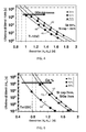
FIG. 4 shows graphs illustrating reduction of NBTI with increasing SiGe thickness. -
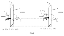
FIG. 5 illustrates energy band diagrams of a standard device and of a semiconductor device according to embodiments of the present invention with increased concentration of the semiconductive element of the semiconductor P-channel layer. -
FIG.6 shows graphs illustrating reduction of NBTI with increased concentration of the semiconductive element of the semiconductor P-channel layer. -
FIG. 7 illustrates energy band diagrams of a standard device and of a semiconductor device according to embodiments of the present invention with decreased thickness of a capping layer between the semiconductor P-channel layer and the gate dielectric. -
FIG. 8 shows graphs illustrating reduction of NBTI with decreased thickness of a capping layer between the semiconductor P-channel layer and the gate dielectric. -
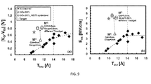
FIG. 9 illustrates principles of the present invention applied to low-EOT devices according to embodiments of the present invention. - The drawings are only schematic and are non-limiting. In the drawings, the size of some of the elements may be exaggerated and not drawn on scale for illustrative purposes.
- Any reference signs in the claims shall not be construed as limiting the scope.
- In the different drawings, the same reference signs refer to the same or analogous elements.
- One way to improve FET performance is by using a strained Si channel layer which incorporates Ge. In embodiments of the present disclosure, the NBTI reliability of, in particular, such SiGe devices is described. This is, however, intended to be an example only, and is not intended to be limiting for the invention.
- NBTI stress experiments were performed on buried SiGe channel P-FETS using the extended-stress-measure technique as described by B. Kaczer et al. in Proc. IEEE IRPS, pp.20-27, 2008. The semiconductor devices under test and a band diagram of this type of semiconductor device in inversion are depicted in
FIG. 1 and FIG. 2 , respectively. - The
semiconductor device 10, also called herein a P-channel semiconductor device, illustrated inFIG. 1 comprises asubstrate 11, e.g. Si substrate, with a semiconductor P-channel layer 12 thereon, e.g. a SiGe P-channel layer. The semiconductor P-channel layer has a valence band energy level Ev(channel). The P-channel semiconductor device 10 furthermore comprises agate dielectric layer 14, e.g. a SiO2 layer, on the semiconductor P-channel layer 12. Thegate dielectric layer 14 has a valence band energy level Agate dielectric). The density of defect levels Et in thegate dielectric layer 14 as function of energy is assumed to be exponentially decreasing from the band edges of the adjacent layer (being the semiconductor P-channel layer 12 or optionally, if present, acapping layer 13 between the P-channel layer 12 and the gate dielectric layer 14) toward the centre of the bandgap of this adjacent layer. - The channel-dielectric band offset ΔEv towards a particular defect level at which charge carriers are injected from the channel into the dielectric is defined as Ev(channel) - Et. The
semiconductor device 10 may furthermore optionally comprise acapping layer 13, e.g. a Si cap, between the P-channel layer 12 and thegate dielectric layer 14 for having a good passivation of the interface, which is advantageous for device performance, a high-k dielectric layer 15, e.g. a HfO2 dielectric layer, and ametal gate 16. - The corresponding energy band diagram is illustrated in
FIG. 2 for an exemplary semiconductor device according to embodiments comprising a SiGe p-channel layer, a Si capping layer and a gate stack comprising a metal gate (MG), a SiO2 dielectric layer and HfO2 dielectric layer. The channel-dielectric band offset ΔEv is indicated. - In accordance with embodiments of the present invention, the
semiconductor device 10 is by purpose engineered such that the inversion carrier injection into the distribution of defect levels occurs as close as possible to the centre of the bandgap of a layer adjacent the gate dielectric layer at the side of the P-channel layer(the semiconductor P-channel layer 12 itself or optionally the capping layer 13). Alternatively worded, in accordance with embodiments of the present invention, the inversion carrier injection level does deviate from the energy level at the centre of the bandgap of the adjacent layer (the semiconductor P-channel layer 12 or optionally the capping layer 13) with a value not more than 49%, such as not more than 40%, for example not more than 20%, not more than 10%, even not more than 5% of that bandgap (in eV). If this is the case, the gate dielectric defect energy level is actually decoupled from the majority carriers in the channel, which are holes as the channel under consideration is of P-type, because of the low concentration of defects at that energy level. In order to obtain this decoupling, in accordance with embodiments of the present invention, parameters of thesemiconductor device 10 are selected such that holes from the semiconductor P-channel layer are prevented from interacting with the gate dielectric defect energy level. This may be obtained by engineering the semiconductor device such that the inversion carrier injection into the distribution of defect levels is so as to avoid interaction between carriers and a high concentration in the distribution of defect levels. This allows reducing NBTI (holes do not "see" the defect level). In particular, the closer the inversion carrier injection into the distribution of defect levels is to the centre of the bandgap of the layer adjacent the gate dielectric layer at the side of the P-channel layer, the better the result in terms of NBTI reliability, as the centre of the bandgap corresponds to the lowest distribution level (concentration) of charge traps. This way, an ad hoc optimization of semiconductor devices, for example SiGe semiconductor devices, provides a solution to the NBTI problem, in particular also for sub-1 nm EOT devices, thus significantly increasing operating overdrive voltages while still guaranteeing 10 year device lifetime. - In one embodiment, selecting parameters of the P-channel semiconductor device such that the inversion carrier injection into the distribution of defect levels does deviate from the energy level at the centre of the bandgap of the adjacent layer with a value not more than 49%, such as not more than 40%, for example not more than 20%, not more than 10%, even not more than 5% of that bandgap (in eV) comprises increasing the thickness of the semiconductor P-
channel layer 12. The energy band diagrams of this embodiment are illustrated inFIG. 3 . The left hand side ofFIG.3 illustrates the energy band diagram of a standard SiGe semiconductor device, having a thinner semiconductor P-channel layer 12, while the right hand side ofFIG. 3 illustrates the energy band diagram of a gate stack in accordance with embodiments of the present invention, where the thickness of the semiconductor P-channel layer 12 is increased. Suitable thicknesses of the semiconductor P-channel layer 12, in case the semiconductor P-channel layer is a SiGe layer, are between a few mono-layers and about 20 nm. This upper limit corresponds to the critical thickness for which the SiGe layer relaxes and loses its compressive strain. InFIG. 3 , the defect level distribution responsible for NBTI is indicated by 30. Thisdefect level distribution 30 corresponds to energy levels and corresponding defect concentrations for a specific example of a SiGe P-FET device. The energy bands of the semiconductor P-channel layer 12, indicated by 31 inFIG. 3 , correspond to a specific example of a SiGe semiconductor P-channel with a particular Ev(channel) of a particular SiGe P-FET device. The energy bands of thegate dielectric layer 14, indicated by 32 inFIG. 3 , correspond to a specific example of a SiO2 gate dielectric layer with a valence band energy level Ev(gate dielectric) of a particular example of a SiGe P-FET device. - It can be seen from
FIG. 4 that increasing the thickness of the semiconductor P-channel layer 12, e.g. SiGe layer, has a positive impact on the NBTI reliability.FIG.4 shows graphs setting out lifetime of devices in function of |VG - Vth|. Lifetime is defined at that moment in time when the device exhibits a 30 mV shift in the threshold voltage Vth. - Graphs are set out for three different SiGe semiconductor devices: a first device with a SiGe layer of 3 nm thickness (graph 40), a second device with a SiGe layer of 5 nm thickness (graph 41) and a third device with a SiGe layer of 7 nm thickness (graph 42). The SiGe layer comprises Germanium as a smallest bandgap semiconductive element with a concentration of 55%, the Si capping layers is 1.3 nm thick. The first device, in order to have a lifetime of 10 years, cannot be allowed to have a |VG - Vth| larger than 0.85 V. For the second device, the |VG - Vth| cannot be larger than 0.92 V and for the third device, the |VG - Vth| should not be larger than 1.01 V in order for these to have a lifetime of 10 years. Hence, the larger the thickness of the semiconductor P-channel layer, the more the NBTI is reduced.
- In another embodiment, selecting parameters of the P-channel semiconductor device such that the inversion carrier injection into the distribution of defect levels does deviate from the energy level at the centre of the bandgap of the adjacent layer with a value not more than 49%, such as not more than 40%, for example not more than 20%, not more than 10%, even not more than 5% of that bandgap (in eV) comprises increasing the fraction of the smallest bandgap semiconductive element of the semiconductor P-
channel layer 12 in case the semiconductor P-channel layer 12 comprises a combination of semiconductive elements, e.g. the Ge concentration in the SiGe layer. The energy band diagrams of this embodiment are illustrated inFIG. 5 . The left hand side ofFIG. 5 illustrates the energy band diagram of a standard semiconductor device, having a lower fraction of the smallest bandgap semiconductive element in the semiconductor P-channel layer 12, while the right hand side ofFIG. 5 illustrates the energy band diagram of a semiconductor device in accordance with embodiments of the present invention, where the fraction of the semiconductive element in the semiconductor P-channel layer 12 is increased. Suitable fractions of the semiconductive element in the semiconductor P-channel layer 12 are between 25 and 99%, for example between 45 and 75%, such as between 55 and 65%. InFIG. 5 , the defect level distribution responsible for NBTI is indicated by 50. Thisdefect level distribution 50 corresponds to energy levels and corresponding defect concentrations for a specific example of a SiGe P-FET device. The energy bands of the semiconductor P-channel layer 12, indicated by 51 inFIG.5 , correspond to a specific example of a SiGe semiconductor P-channel with a particular Ev(channel) of a particular SiGe P-FET device. The energy bands of thegate dielectric layer 14, indicated by 52 inFIG. 5 , correspond to a specific example of a SiO2 gate dielectric layer with a valence band energy level Ev(gate dielectric) of a particular example of a SiGe P-FET device. - It can be seen from
FIG.6 that increasing the concentration of the smallest bandgap semiconductive element of the semiconductor P-channel layer 12, in the embodiment illustrated e.g. increasing the Ge content in a SiGe layer, has a positive impact on the NBTI reliability.FIG. 6 shows graphs setting out lifetime of devices in function of |VG - Vth|. Lifetime is defined at that moment in time when the device exhibits a 30 mV shift in the threshold voltage Vth. - Graphs are set out for three different semiconductor devices: a fourth device with a Ge content in the SiGe layer of 0% (graph 60), a fifth device with a Ge content in the SiGe layer of 45% (graph 61) and a sixth device with a Ge content in the SiGe layer of 55% (graph 62). The thickness of the SiGe layer is about 7 nm and the thickness of the Si capping layer is about 2 nm. The fourth device, in order to have a lifetime of 10 years, cannot be allowed to have a |VG - Vth| larger than 0.46 V. For the fifth device, the |VG - Vth| cannot be larger than 0.8 V and for the sixth device, the |VG - Vth| should not be larger than 1.01 V in order for it to have a lifetime of 10 years. Hence, the larger the fraction of the smallest bandgap semiconductive material in the semiconductor P-
channel layer 12, e.g. the larger the Ge content in the SiGe layer, the more the NBTI is reduced. - In yet another embodiment, selecting parameters of the P-channel semiconductor device such that the inversion carrier injection into the distribution of defect levels does deviate from the energy level at the centre of the bandgap of the adjacent layer with a value not more than 49%, such as not more than 40%, for example not more than 20%, not more than 10%, even not more than 5% of that bandgap (in eV) comprises decreasing the thickness of the
capping layer 13 on the semiconductor P-channel layer 12, e.g. the Si capping layer thickness. The energy band diagrams of this embodiment are illustrated inFIG. 7 . The left hand side ofFIG.7 illustrates the energy band diagram of a standard semiconductor device, having a thicker capping layer, while the right hand side ofFIG. 7 illustrates the energy band diagram of a semiconductor device in accordance with embodiments of the present invention, having a thinner capping layer. Suitable thicknesses of the capping layer are between 0 nm and 5 nm, e.g. between 0.1 nm and 5 nm, such as between 0.65 nm and 3 nm. InFIG. 7 , the defect level distribution responsible for NBTI is indicated by 70. Thisdefect level distribution 70 corresponds to energy levels and corresponding defect concentrations for a specific example of a SiGe P-FET device. The energy bands of the semiconductor P-channel layer 12, indicated by 71 inFIG. 7 , correspond to a specific example of a SiGe semiconductor P-channel with a particular Ev(channel) of a particular SiGe P-FET device. The energy bands of thegate dielectric layer 14, indicated by 72 inFIG. 7 , correspond to a specific example of a SiO2 gate dielectric layer with a valence band energy level Ev(gate dielectric) of a particular example of a SiGe P-FET device. The energy bands of thecapping layer 13, indicated by 73 inFIG. 7 , correspond to a specific example of a Si capping layer. - It can be seen from
FIG. 8 that decreasing the thickness of the cap, e.g. decreasing the Si cap thickness, has a positive impact on the NBTI reliability.FIG. 8 shows graphs setting out lifetime of devices in function of |VG - Vth|. Lifetime is defined at that moment in time when the device exhibits a 30 mV shift in the threshold voltage Vth. - Graphs are set out for four different devices: a seventh device with a Si cap thickness of 0.65 nm (graph 80), an eighth device with a Si cap thickness of 1 nm (graph 81), a ninth device with a Si cap thickness of 1.3 nm (graph 82) and a tenth device with a Si cap thickness of 2 nm (graph 83). In the embodiments illustrated, the Ge content of the SiGe layer is about 55%. The thickness of the SiGe layer is about 5 nm. The tenth device, in order to have a lifetime of 10 years, cannot be allowed to have a |VG - Vth| larger than 0.81 V. For the ninth device, the |VG - Vth| cannot be larger than 0.9 V, for the eighth device, the |VG - Vth| cannot be larger than 1.08 V and for the seventh device, the |VG - Vth| should not be larger than 1.15 V in order for these to have a lifetime of 10 years. Hence, the smaller the cap thickness, e.g. the thinner the Si cap, the more the NBTI is reduced. Nevertheless, using no Si cap when using a SiGe channel layer leads to very bad interface passivation. The NBTI reliability of the device would still be good, but the device performance would be poor. Hence a trade-off between device passivation and NBTI reliability needs to be made.
- An example of a P-channel semiconductor device according to embodiments of the present invention may be a SiGe-channel P-FET comprising a Si capping layer in between the buried SiGe channel layer and a SiO2 gate dielectric layer. More details for this example are presented hereinafter.
- NBTI stress experiments were performed on buried SiGe channel P-FETS using the extended-stress-measure technique as described by B. Kaczer et al. in Proc. IEEE IRPS, pp.20-27, 2008. The gate stack of devices under test and a band diagram of this type of stack in inversion are depicted in
FIG. 1 and FIG. 2 , respectively. Three major parameters were varied separately in order to assess their impact on NBTI reliability, i.e. the Ge concentration, the SiGe layer thickness and the Si cap thickness. Ge content varied from 0% (pure Si channel reference) up to 55%; SiGe layer thickness varied between 3 and 7 nm; Si cap thickness after oxidation, as estimated by C-V curves and TEM pictures, varied between 0.65 and 2 nm. It should be noted that the thickness of the Si cap impacts the EOT and Cox values, and hence a fixed overdrive voltage leads to different oxide electric fields Eox for different devices. This may affect interpretation of NBTI data. So, to have a more fair comparison, degradation (ΔNeff = ΔVth * Cox/q) should be compared as a function of the equivalent Eox for different Si thicknesses. Having two dielectrics (SiO2 and high-k HfO2, the electric field is different on each of these. An equivalent Eox is calculated from the EOT, equivalent to the Eox that a SiO2 dielectric with thickness equal to the EOT of the stack would experience. Equivalent Eox extraction is not trivial for such complex gate stacks. For the experiments it has been extracted with the following method in order to be on a safe side: Q-V curve is obtained integrating C-V curve; a line is fitted to the linear part of the Q-V curve; the slope of the line represents the extracted Cox; EOT is calculated from Cox; finally the equivalent Eox is calculated as |VG-Vth|/EOT. - A wide set of experiments were performed on SiGe p-FETS changing only one of the semiconductor device parameters (i.e. the concentration of the semiconductive element and/or the thickness of the channel layer and/or the thickness of the capping layer) under investigation at the time, while fixing the other two. The following observations are made:
- 1) As is shown in
FIG.6 , the introduction of semiconductive material in the channel, the semiconductive material having a bandgap smaller than the bandgap of the original channel material, e.g. introduction of Ge in a Si channel, dramatically improves the NBTI reliability. Extrapolated operating overdrive voltage for 10 years lifetime (Vop) assuming 30 mV threshold voltage shift (ΔVth) at 125°C criterion, increases from 0.46 V for the pure Si reference up to 0.92 V for 55% Ge concentration. - 2) Increasing the thickness of the P-type channel material, e.g. SiGe layer, has also a positive impact on the NBTI reliability (
FIG. 4 ): Vop increases from 0.85 V up to 1.01 V when moving from a 3 nm thick SiGe layer to a 7 nm thick one. - 3) The capping layer, e.g. Si cap, has also an important impact on NBTI reliability (
FIG. 8 ). A thicker capping layer, e.g. Si cap, clearly degrades the NBTI performance. Vop moves between 0.83 V and 1.13 V as a function of the Si cap thickness. To exclude the effect of varying EOT,FIG. 9 shows the degradation (ΔNeff = ΔVth * Cox/q) vs. Eox. It can be seen that the impact of the Si cap thickness is not an artifact due to different EOT. - Surprisingly, embodiments of the present invention apply also to ultra-thin EOT semiconductor devices, e.g. semiconductor devices with an EOT below 1 nm. This is absolutely not trivial, since ultra-thin EOT devices are implemented by consumption of the gate dielectric interfacial layer, e.g. SiO2 layer, which is known to be detrimental for reliability.
- In a particular experiment, a 6Å EOT Si0.45Ge0.55 P-FET with 10 year lifetime at operating conditions (VDD = 1 V) has been demonstrated. Ultra-thin EOT is achieved by interfacial layer (IL) scavenging. NBTI is alleviated using a high Ge fraction, a thick SiGe quantum well (QW) and a thin Si capping layer as set out above.
- In particular the Si capping layer has a considerable impact on the NBTI reliability with thinner cappping layers enhancing the lifetime. EOT reduction by IL scavenging degrades the NBTI reliability faster than high-k scaling. In particular, there is an additional reliability deterioration on top of that caused by the electric field increase due to EOT scaling (maximum operating Eox vs. Tinv would stay constant as observed for thick EOT Si devices).
-
FIG. 9 illustrates that a high Ge fraction (55%) and a thick SiGe layer (6.5 nm) combined with the use of a thin Si cap (0.8 nm) boost NBTI lifetime to meet the target condition (|VG-Vth|=0.7 V at Tinv = 10 Å, EOT ∼ 6 Å) on devices implementing aggressive IL scavenging. - While the invention has been illustrated and described in detail in the drawings and foregoing description, such illustration and description are to be considered illustrative or exemplary and not restrictive. The invention is not limited to the disclosed embodiments.
- The foregoing description details certain embodiments of the invention. It will be appreciated, however, that no matter how detailed the foregoing appears in text, the invention may be practiced in many ways. It should be noted that the use of particular terminology when describing certain features or aspects of the invention should not be taken to imply that the terminology is being re-defined herein to be restricted to include any specific characteristics of the features or aspects of the invention with which that terminology is associated.
Claims (14)
- A method for forming a P-channel semiconductor device with good NBTI reliability,
the method comprising providing a P-channel semiconductor device comprising a P-channel layer, and a control electrode on the semiconductor P-channel layer comprising at least a gate dielectric layer, the gate dielectric layer having an exponentially-shaped distribution of defect levels E(defect) in the energy bandgap, the exponentially-shaped distribution of defect levels having a lower concentration of defect levels at the centre of the bandgap and a higher concentration of defect levels at the edges of the bandgap,
wherein the method comprises selecting at least one parameter of the P-channel semiconductor device such that the inversion carrier injection into the distribution of defect levels does deviate from the energy level at the centre of the bandgap of a layer adjacent the gate dielectric layer at the same side of the gate dielectric layer as the P-channel layer, with a value not more than 49% of that bandgap in eV. - A method according to claim 1, wherein selecting at least one parameter of the P-channel semiconductor device comprises selecting the thickness of the semiconductor P-channel layer between a few mono-layers and 20 nm.
- A method according to claim 2, wherein selecting at least one parameter of the P-channel semiconductor device comprises selecting the thickness of the semiconductor P-channel layer higher than 3 nm.
- A method according to any of the previous claims, the semiconductor P-channel layer comprising a combination of at least two semiconductive elements, one of the semiconductive elements having a smaller bandgap than the others, wherein selecting parameters of the P-channel semiconductor device comprises selecting the concentration in the semiconductor P-channel layer of the semiconductive element with the smallest bandgap between 25% and 99%.
- A method according to claim 4, wherein selecting at least one parameter of the P-channel semiconductor device comprises selecting the concentration in the semiconductor P-channel layer of the semiconductive element with the smallest bandgap higher than 50%.
- A method according to any of the previous claims, the P-channel semiconductor device comprising a semiconductor capping layer in between the semiconductor P-channel layer and the gate dielectric layer, wherein selecting parameters of the P-channel semiconductor device comprises selecting the thickness of the semiconductor capping layer between 0.1 nm and 5 nm.
- A method according to claim 6, wherein selecting at least one parameter of the P-channel semiconductor device comprises selecting the thickness of the semiconductor capping layer 2 nm or below.
- A P-channel semiconductor device comprising a semiconductor P-channel layer, and a control electrode on the semiconductor P-channel layer comprising at least a gate dielectric layer, the gate dielectric layer having an exponentially-shaped distribution of defect levels E(defect) in the energy bandgap, the exponentially-shaped distribution of defect levels having a lower concentration of defect levels at the centre of the bandgap and a higher concentration of defect levels at the edges of the bandgap, the P-channel semiconductor device having an inversion carrier injection into the distribution of defect levels which does deviate from the energy level at the centre of the bandgap of a layer adjacent the gate dielectric layer at the same side of the gate dielectric layer as the P-channel layer, with a value not more than 49% of that bandgap in eV.
- A P-channel semiconductor device according to claim 8, wherein the P-channel layer comprises a combination of at least two semiconductive elements.
- A P-channel semiconductor device according to claim 9, wherein the P-channel layer is a SiGe layer.
- A P-channel semiconductor device according to any of claims 8 to 10, wherein the thickness of the semiconductor P-channel layer is higher than 3 nm.
- A P-channel semiconductor device according to any of claims 9 to 11, one of the semiconductive elements having a smaller bandgap than the others, wherein the concentration in the semiconductor P-channel layer of the semiconductive element with the smallest bandgap is higher than 50%.
- A P-channel semiconductor device according to any of claims 8 to 12, the P-channel semiconductor device comprising a capping layer between the semiconductor P-channel layer and the gate dielectric layer, wherein the thickness of the capping layer is 2 nm or below.
- A P-channel semiconductor device according to any of claims 8 to 13, having a sub-1 nm EOT.
Applications Claiming Priority (1)
| Application Number | Priority Date | Filing Date | Title |
|---|---|---|---|
| US25040909P | 2009-10-09 | 2009-10-09 |
Publications (2)
| Publication Number | Publication Date |
|---|---|
| EP2309543A1 true EP2309543A1 (en) | 2011-04-13 |
| EP2309543B1 EP2309543B1 (en) | 2012-05-09 |
Family
ID=43430712
Family Applications (1)
| Application Number | Title | Priority Date | Filing Date |
|---|---|---|---|
| EP10186985A Active EP2309543B1 (en) | 2009-10-09 | 2010-10-08 | Method for enhancing the reliability of a P-channel semiconductor device and a P-channel semiconductor device made thereof |
Country Status (4)
| Country | Link |
|---|---|
| US (1) | US8062962B2 (en) |
| EP (1) | EP2309543B1 (en) |
| JP (1) | JP2011082527A (en) |
| AT (1) | ATE557424T1 (en) |
Families Citing this family (3)
| Publication number | Priority date | Publication date | Assignee | Title |
|---|---|---|---|---|
| KR102122464B1 (en) | 2013-11-29 | 2020-06-12 | 삼성전자 주식회사 | Method of preventing nbti effect using self refresh information |
| CN106847918B (en) * | 2015-12-04 | 2022-01-07 | Imec 非营利协会 | Ge Field Effect Transistor (FET) and method of manufacture |
| KR102756342B1 (en) * | 2022-05-03 | 2025-01-16 | 성균관대학교산학협력단 | Junction structure element, method for manufacturing the same and computing device comprising the same |
Family Cites Families (1)
| Publication number | Priority date | Publication date | Assignee | Title |
|---|---|---|---|---|
| JP2007287913A (en) * | 2006-04-17 | 2007-11-01 | Matsushita Electric Ind Co Ltd | Field effect transistor and manufacturing method thereof |
-
2010
- 2010-10-08 EP EP10186985A patent/EP2309543B1/en active Active
- 2010-10-08 AT AT10186985T patent/ATE557424T1/en active
- 2010-10-12 US US12/903,040 patent/US8062962B2/en active Active
- 2010-10-12 JP JP2010229445A patent/JP2011082527A/en active Pending
Non-Patent Citations (7)
| Title |
|---|
| AOULAICHE M ET AL: "Negative bias temperature instability on Si-passivated Ge-interface", 2008 IEEE INTERNATIONAL RELIABILITY PHYSICS SYMPOSIUM (IRPS) IEEE PISCATAWAY, NJ, USA, 2008, pages 358 - 362, XP002617040, ISBN: 978-1-4244-2049-0 * |
| B. KACZER ET AL., PROC. IEEE IRPS, 2008, pages 20 - 27 |
| FRANCO J ET AL: "Improvements of NBTI reliability in SiGe p-FETs", 2010 IEEE INTERNATIONAL RELIABILITY PHYSICS SYMPOSIUM (IRPS 2010) IEEE PISCATAWAY, NJ, USA, 2010, pages 1082 - 1085, XP002617041, ISBN: 978-1-4244-5430-3 * |
| GRASSER T ET AL: "A two-stage model for negative bias temperature instability", 2009 IEEE INTERNATIONAL RELIABILITY PHYSICS SYMPOSIUM (IRPS) IEEE PISCATAWAY, NJ, USA, 26 April 2009 (2009-04-26) - 30 April 2009 (2009-04-30), pages 33 - 44, XP002617039, ISBN: 978-1-4244-2889-2 * |
| KACZER B ET AL: "NBTI from the perspective of defect states with widely distributed time scales", 2009 IEEE INTERNATIONAL RELIABILITY PHYSICS SYMPOSIUM (IRPS) IEEE PISCATAWAY, NJ, USA, 26 April 2009 (2009-04-26) - 30 April 2009 (2009-04-30), pages 55 - 60, XP002617038, ISBN: 978-1-4244-2889-2 * |
| MORSHED T H ET AL: "Physics-based 1/f noise model for MOSFETs with nitrided high-kappa gate dielectrics", SOLID STATE ELECTRONICS, ELSEVIER SCIENCE PUBLISHERS, BARKING, GB, vol. 52, no. 5, 1 May 2008 (2008-05-01), pages 711 - 724, XP022587020, ISSN: 0038-1101, [retrieved on 20071126] * |
| SE-HOON LEE ET AL: "Demonstration of pMOSFETs With Channels, High , and Controlled Short Channel Effects (SCEs)", IEEE ELECTRON DEVICE LETTERS, IEEE SERVICE CENTER, NEW YORK, NY, US, vol. 29, no. 9, 1 September 2008 (2008-09-01), pages 1017 - 1020, XP011233576, ISSN: 0741-3106 * |
Also Published As
| Publication number | Publication date |
|---|---|
| ATE557424T1 (en) | 2012-05-15 |
| US20110084309A1 (en) | 2011-04-14 |
| EP2309543B1 (en) | 2012-05-09 |
| US8062962B2 (en) | 2011-11-22 |
| JP2011082527A (en) | 2011-04-21 |
Similar Documents
| Publication | Publication Date | Title |
|---|---|---|
| Batude et al. | Demonstration of low temperature 3D sequential FDSOI integration down to 50 nm gate length | |
| Pillarisetty | Academic and industry research progress in germanium nanodevices | |
| Saraswat et al. | High mobility materials and novel device structures for high performance nanoscale MOSFETs | |
| Kamata | High-k/Ge MOSFETs for future nanoelectronics | |
| Cartier et al. | Role of oxygen vacancies in V/sub FB//V/sub t/stability of pFET metals on HfO/sub 2 | |
| US10680108B2 (en) | Field-effect transistor comprising germanium and manufacturing method thereof | |
| Villalon et al. | First demonstration of strained SiGe nanowires TFETs with ION beyond 700µA/µm | |
| Alshareef et al. | Thermally stable N-metal gate MOSFETs using La-incorporated HfSiO dielectric | |
| US8933488B2 (en) | Heterostructure field effect transistor with same channel and barrier configuration for PMOS and NMOS | |
| CN111261715A (en) | pMOS transistor including a low thermal budget gate stack | |
| US7728387B1 (en) | Semiconductor device with high on current and low leakage | |
| Franco et al. | NBTI in replacement metal gate SiGe core FinFETs: Impact of Ge concentration, fin width, fin rotation and interface passivation by high pressure anneals | |
| Kim et al. | In 0.53 Ga 0.47 As-on-insulator metal–oxide–semiconductor field-effect transistors utilizing Y 2 O 3 buried oxide | |
| Franco et al. | Demonstration of an InGaAs gate stack with sufficient PBTI reliability by thermal budget optimization, nitridation, high-k material choice, and interface dipole | |
| EP2309543B1 (en) | Method for enhancing the reliability of a P-channel semiconductor device and a P-channel semiconductor device made thereof | |
| Zhu et al. | Performance enhancement of GaSb vertical nanowire p-type MOSFETs on Si by rapid thermal annealing | |
| Franco et al. | 6Å EOT Si 0.45 Ge 0.55 pMOSFET with optimized reliability (V DD= 1V): Meeting the NBTI lifetime target at ultra-thin EOT | |
| KR101262504B1 (en) | Density of states engineered field effect transistor | |
| Toriumi | Recent progress of germanium MOSFETs | |
| Ikeda et al. | Enhancement of hole mobility and cut-off characteristics of strained Ge nanowire pMOSFETs by using plasma oxidized GeOx inter-layer for gate stack | |
| Sioncke et al. | First demonstration of∼ 3500 cm 2/Vs electron mobility and sufficient BTI reliability (max V ov up to 0.6 V) In 0.53 Ga 0.47 As nFET using an IL/LaSiO x/HfO 2 gate stack | |
| Deora et al. | Positive bias instability in gate-first and gate-last InGaAs channel n-MOSFETs | |
| Kamata et al. | High-k/Ge p-& n-MISFETs with strontium germanide interlayer for EOT scalable CMIS application | |
| Wrachien et al. | Effects of Positive and Negative Stresses on III–V MOSFETs With $\hbox {Al} _ {2}\hbox {O} _ {3} $ Gate Dielectric | |
| Guo et al. | Improving switching performance of thin-film transistors in disordered silicon |
Legal Events
| Date | Code | Title | Description |
|---|---|---|---|
| PUAI | Public reference made under article 153(3) epc to a published international application that has entered the european phase |
Free format text: ORIGINAL CODE: 0009012 |
|
| AK | Designated contracting states |
Kind code of ref document: A1 Designated state(s): AL AT BE BG CH CY CZ DE DK EE ES FI FR GB GR HR HU IE IS IT LI LT LU LV MC MK MT NL NO PL PT RO RS SE SI SK SM TR |
|
| AX | Request for extension of the european patent |
Extension state: BA ME |
|
| 17P | Request for examination filed |
Effective date: 20111007 |
|
| GRAP | Despatch of communication of intention to grant a patent |
Free format text: ORIGINAL CODE: EPIDOSNIGR1 |
|
| RIC1 | Information provided on ipc code assigned before grant |
Ipc: H01L 29/49 20060101ALN20111118BHEP Ipc: H01L 29/51 20060101ALI20111118BHEP Ipc: H01L 29/10 20060101AFI20111118BHEP |
|
| GRAS | Grant fee paid |
Free format text: ORIGINAL CODE: EPIDOSNIGR3 |
|
| GRAA | (expected) grant |
Free format text: ORIGINAL CODE: 0009210 |
|
| AK | Designated contracting states |
Kind code of ref document: B1 Designated state(s): AL AT BE BG CH CY CZ DE DK EE ES FI FR GB GR HR HU IE IS IT LI LT LU LV MC MK MT NL NO PL PT RO RS SE SI SK SM TR |
|
| REG | Reference to a national code |
Ref country code: GB Ref legal event code: FG4D |
|
| REG | Reference to a national code |
Ref country code: CH Ref legal event code: EP Ref country code: AT Ref legal event code: REF Ref document number: 557424 Country of ref document: AT Kind code of ref document: T Effective date: 20120515 |
|
| REG | Reference to a national code |
Ref country code: IE Ref legal event code: FG4D |
|
| REG | Reference to a national code |
Ref country code: DE Ref legal event code: R096 Ref document number: 602010001458 Country of ref document: DE Effective date: 20120705 |
|
| REG | Reference to a national code |
Ref country code: NL Ref legal event code: VDEP Effective date: 20120509 |
|
| REG | Reference to a national code |
Ref country code: LT Ref legal event code: MG4D Effective date: 20120509 |
|
| PG25 | Lapsed in a contracting state [announced via postgrant information from national office to epo] |
Ref country code: FI Free format text: LAPSE BECAUSE OF FAILURE TO SUBMIT A TRANSLATION OF THE DESCRIPTION OR TO PAY THE FEE WITHIN THE PRESCRIBED TIME-LIMIT Effective date: 20120509 Ref country code: NO Free format text: LAPSE BECAUSE OF FAILURE TO SUBMIT A TRANSLATION OF THE DESCRIPTION OR TO PAY THE FEE WITHIN THE PRESCRIBED TIME-LIMIT Effective date: 20120809 Ref country code: LT Free format text: LAPSE BECAUSE OF FAILURE TO SUBMIT A TRANSLATION OF THE DESCRIPTION OR TO PAY THE FEE WITHIN THE PRESCRIBED TIME-LIMIT Effective date: 20120509 Ref country code: CY Free format text: LAPSE BECAUSE OF FAILURE TO SUBMIT A TRANSLATION OF THE DESCRIPTION OR TO PAY THE FEE WITHIN THE PRESCRIBED TIME-LIMIT Effective date: 20120509 Ref country code: SE Free format text: LAPSE BECAUSE OF FAILURE TO SUBMIT A TRANSLATION OF THE DESCRIPTION OR TO PAY THE FEE WITHIN THE PRESCRIBED TIME-LIMIT Effective date: 20120509 Ref country code: PL Free format text: LAPSE BECAUSE OF FAILURE TO SUBMIT A TRANSLATION OF THE DESCRIPTION OR TO PAY THE FEE WITHIN THE PRESCRIBED TIME-LIMIT Effective date: 20120509 Ref country code: RS Free format text: LAPSE BECAUSE OF FAILURE TO SUBMIT A TRANSLATION OF THE DESCRIPTION OR TO PAY THE FEE WITHIN THE PRESCRIBED TIME-LIMIT Effective date: 20120509 Ref country code: IS Free format text: LAPSE BECAUSE OF FAILURE TO SUBMIT A TRANSLATION OF THE DESCRIPTION OR TO PAY THE FEE WITHIN THE PRESCRIBED TIME-LIMIT Effective date: 20120909 |
|
| REG | Reference to a national code |
Ref country code: AT Ref legal event code: MK05 Ref document number: 557424 Country of ref document: AT Kind code of ref document: T Effective date: 20120509 |
|
| PG25 | Lapsed in a contracting state [announced via postgrant information from national office to epo] |
Ref country code: GR Free format text: LAPSE BECAUSE OF FAILURE TO SUBMIT A TRANSLATION OF THE DESCRIPTION OR TO PAY THE FEE WITHIN THE PRESCRIBED TIME-LIMIT Effective date: 20120810 Ref country code: LV Free format text: LAPSE BECAUSE OF FAILURE TO SUBMIT A TRANSLATION OF THE DESCRIPTION OR TO PAY THE FEE WITHIN THE PRESCRIBED TIME-LIMIT Effective date: 20120509 Ref country code: SI Free format text: LAPSE BECAUSE OF FAILURE TO SUBMIT A TRANSLATION OF THE DESCRIPTION OR TO PAY THE FEE WITHIN THE PRESCRIBED TIME-LIMIT Effective date: 20120509 Ref country code: HR Free format text: LAPSE BECAUSE OF FAILURE TO SUBMIT A TRANSLATION OF THE DESCRIPTION OR TO PAY THE FEE WITHIN THE PRESCRIBED TIME-LIMIT Effective date: 20120509 Ref country code: PT Free format text: LAPSE BECAUSE OF FAILURE TO SUBMIT A TRANSLATION OF THE DESCRIPTION OR TO PAY THE FEE WITHIN THE PRESCRIBED TIME-LIMIT Effective date: 20120910 |
|
| PG25 | Lapsed in a contracting state [announced via postgrant information from national office to epo] |
Ref country code: BE Free format text: LAPSE BECAUSE OF FAILURE TO SUBMIT A TRANSLATION OF THE DESCRIPTION OR TO PAY THE FEE WITHIN THE PRESCRIBED TIME-LIMIT Effective date: 20120509 |
|
| PG25 | Lapsed in a contracting state [announced via postgrant information from national office to epo] |
Ref country code: EE Free format text: LAPSE BECAUSE OF FAILURE TO SUBMIT A TRANSLATION OF THE DESCRIPTION OR TO PAY THE FEE WITHIN THE PRESCRIBED TIME-LIMIT Effective date: 20120509 Ref country code: NL Free format text: LAPSE BECAUSE OF FAILURE TO SUBMIT A TRANSLATION OF THE DESCRIPTION OR TO PAY THE FEE WITHIN THE PRESCRIBED TIME-LIMIT Effective date: 20120509 Ref country code: SK Free format text: LAPSE BECAUSE OF FAILURE TO SUBMIT A TRANSLATION OF THE DESCRIPTION OR TO PAY THE FEE WITHIN THE PRESCRIBED TIME-LIMIT Effective date: 20120509 Ref country code: RO Free format text: LAPSE BECAUSE OF FAILURE TO SUBMIT A TRANSLATION OF THE DESCRIPTION OR TO PAY THE FEE WITHIN THE PRESCRIBED TIME-LIMIT Effective date: 20120509 Ref country code: DK Free format text: LAPSE BECAUSE OF FAILURE TO SUBMIT A TRANSLATION OF THE DESCRIPTION OR TO PAY THE FEE WITHIN THE PRESCRIBED TIME-LIMIT Effective date: 20120509 Ref country code: AT Free format text: LAPSE BECAUSE OF FAILURE TO SUBMIT A TRANSLATION OF THE DESCRIPTION OR TO PAY THE FEE WITHIN THE PRESCRIBED TIME-LIMIT Effective date: 20120509 Ref country code: CZ Free format text: LAPSE BECAUSE OF FAILURE TO SUBMIT A TRANSLATION OF THE DESCRIPTION OR TO PAY THE FEE WITHIN THE PRESCRIBED TIME-LIMIT Effective date: 20120509 |
|
| PG25 | Lapsed in a contracting state [announced via postgrant information from national office to epo] |
Ref country code: IT Free format text: LAPSE BECAUSE OF FAILURE TO SUBMIT A TRANSLATION OF THE DESCRIPTION OR TO PAY THE FEE WITHIN THE PRESCRIBED TIME-LIMIT Effective date: 20120509 |
|
| PLBE | No opposition filed within time limit |
Free format text: ORIGINAL CODE: 0009261 |
|
| STAA | Information on the status of an ep patent application or granted ep patent |
Free format text: STATUS: NO OPPOSITION FILED WITHIN TIME LIMIT |
|
| 26N | No opposition filed |
Effective date: 20130212 |
|
| PG25 | Lapsed in a contracting state [announced via postgrant information from national office to epo] |
Ref country code: ES Free format text: LAPSE BECAUSE OF FAILURE TO SUBMIT A TRANSLATION OF THE DESCRIPTION OR TO PAY THE FEE WITHIN THE PRESCRIBED TIME-LIMIT Effective date: 20120820 |
|
| PG25 | Lapsed in a contracting state [announced via postgrant information from national office to epo] |
Ref country code: MC Free format text: LAPSE BECAUSE OF NON-PAYMENT OF DUE FEES Effective date: 20121031 |
|
| REG | Reference to a national code |
Ref country code: DE Ref legal event code: R097 Ref document number: 602010001458 Country of ref document: DE Effective date: 20130212 |
|
| REG | Reference to a national code |
Ref country code: IE Ref legal event code: MM4A |
|
| PG25 | Lapsed in a contracting state [announced via postgrant information from national office to epo] |
Ref country code: BG Free format text: LAPSE BECAUSE OF FAILURE TO SUBMIT A TRANSLATION OF THE DESCRIPTION OR TO PAY THE FEE WITHIN THE PRESCRIBED TIME-LIMIT Effective date: 20120809 Ref country code: IE Free format text: LAPSE BECAUSE OF NON-PAYMENT OF DUE FEES Effective date: 20121008 |
|
| PG25 | Lapsed in a contracting state [announced via postgrant information from national office to epo] |
Ref country code: MT Free format text: LAPSE BECAUSE OF FAILURE TO SUBMIT A TRANSLATION OF THE DESCRIPTION OR TO PAY THE FEE WITHIN THE PRESCRIBED TIME-LIMIT Effective date: 20120509 Ref country code: AL Free format text: LAPSE BECAUSE OF FAILURE TO SUBMIT A TRANSLATION OF THE DESCRIPTION OR TO PAY THE FEE WITHIN THE PRESCRIBED TIME-LIMIT Effective date: 20120509 |
|
| PG25 | Lapsed in a contracting state [announced via postgrant information from national office to epo] |
Ref country code: TR Free format text: LAPSE BECAUSE OF FAILURE TO SUBMIT A TRANSLATION OF THE DESCRIPTION OR TO PAY THE FEE WITHIN THE PRESCRIBED TIME-LIMIT Effective date: 20120509 |
|
| PG25 | Lapsed in a contracting state [announced via postgrant information from national office to epo] |
Ref country code: LU Free format text: LAPSE BECAUSE OF NON-PAYMENT OF DUE FEES Effective date: 20121008 Ref country code: SM Free format text: LAPSE BECAUSE OF FAILURE TO SUBMIT A TRANSLATION OF THE DESCRIPTION OR TO PAY THE FEE WITHIN THE PRESCRIBED TIME-LIMIT Effective date: 20120509 |
|
| PG25 | Lapsed in a contracting state [announced via postgrant information from national office to epo] |
Ref country code: HU Free format text: LAPSE BECAUSE OF FAILURE TO SUBMIT A TRANSLATION OF THE DESCRIPTION OR TO PAY THE FEE WITHIN THE PRESCRIBED TIME-LIMIT Effective date: 20101008 |
|
| REG | Reference to a national code |
Ref country code: CH Ref legal event code: PL |
|
| PG25 | Lapsed in a contracting state [announced via postgrant information from national office to epo] |
Ref country code: CH Free format text: LAPSE BECAUSE OF NON-PAYMENT OF DUE FEES Effective date: 20141031 Ref country code: MK Free format text: LAPSE BECAUSE OF FAILURE TO SUBMIT A TRANSLATION OF THE DESCRIPTION OR TO PAY THE FEE WITHIN THE PRESCRIBED TIME-LIMIT Effective date: 20120509 Ref country code: LI Free format text: LAPSE BECAUSE OF NON-PAYMENT OF DUE FEES Effective date: 20141031 |
|
| REG | Reference to a national code |
Ref country code: FR Ref legal event code: PLFP Year of fee payment: 6 |
|
| REG | Reference to a national code |
Ref country code: FR Ref legal event code: PLFP Year of fee payment: 7 |
|
| REG | Reference to a national code |
Ref country code: FR Ref legal event code: PLFP Year of fee payment: 8 |
|
| REG | Reference to a national code |
Ref country code: FR Ref legal event code: PLFP Year of fee payment: 9 |
|
| P01 | Opt-out of the competence of the unified patent court (upc) registered |
Effective date: 20230513 |
|
| REG | Reference to a national code |
Ref country code: DE Ref legal event code: R079 Ref document number: 602010001458 Country of ref document: DE Free format text: PREVIOUS MAIN CLASS: H01L0029100000 Ipc: H10D0062170000 |
|
| PGFP | Annual fee paid to national office [announced via postgrant information from national office to epo] |
Ref country code: GB Payment date: 20250923 Year of fee payment: 16 |
|
| PGFP | Annual fee paid to national office [announced via postgrant information from national office to epo] |
Ref country code: FR Payment date: 20250924 Year of fee payment: 16 |
|
| PGFP | Annual fee paid to national office [announced via postgrant information from national office to epo] |
Ref country code: DE Payment date: 20250923 Year of fee payment: 16 |