EP2309364A2 - Microcomputer - Google Patents
Microcomputer Download PDFInfo
- Publication number
- EP2309364A2 EP2309364A2 EP10013387A EP10013387A EP2309364A2 EP 2309364 A2 EP2309364 A2 EP 2309364A2 EP 10013387 A EP10013387 A EP 10013387A EP 10013387 A EP10013387 A EP 10013387A EP 2309364 A2 EP2309364 A2 EP 2309364A2
- Authority
- EP
- European Patent Office
- Prior art keywords
- light
- microcomputer
- receiving device
- remote control
- control signal
- Prior art date
- Legal status (The legal status is an assumption and is not a legal conclusion. Google has not performed a legal analysis and makes no representation as to the accuracy of the status listed.)
- Withdrawn
Links
Images


Classifications
-
- G—PHYSICS
- G06—COMPUTING OR CALCULATING; COUNTING
- G06F—ELECTRIC DIGITAL DATA PROCESSING
- G06F1/00—Details not covered by groups G06F3/00 - G06F13/00 and G06F21/00
- G06F1/26—Power supply means, e.g. regulation thereof
- G06F1/32—Means for saving power
- G06F1/3203—Power management, i.e. event-based initiation of a power-saving mode
- G06F1/3234—Power saving characterised by the action undertaken
- G06F1/325—Power saving in peripheral device
Definitions
- This invention relates to a microcomputer controlling a light-receiving device that receives a remote control signal from a remote control signal transmitter.
- Remote-controllable electronic equipment such as a TV, a home stereo system or an air conditioner contains a receiving circuit for a remote control signal.
- the remote control signal is received by a light-receiving device, the received remote control signal is waveform-shaped, and the waveform-shaped remote control signal is decoded, so that the remote control signal is interpreted.
- the conventional receiving circuit for the remote control signal samples the remote control signal from the light-receiving device at predetermined intervals, there is a problem of a large amount of power consumption, particularly power consumption by the light-receiving device which is always in operation.
- the object of this invention is directed to reducing the power consumption by the light-receiving device as well as reducing the power consumption by the microcomputer that controls the light-receiving device.
- the invention provides a microcomputer that includes a memory storing a program and a drive circuit driving a switching device.
- the switching device provides a light-receiving device with a power supply, and the light-receiving device receives a remote control signal.
- the microcomputer also includes a CPU executing the program stored in the memory. The CPU is configured to switch off, through the drive circuit, the switching device so that the light-receiving device is not provided with the power supply, to set the microcomputer in a standby state for a predetermined period of time and to switch on, through the drive circuit, the switching device so that the light-receiving device is provided with the power supply when the microcomputer is released from the standby state.
- the invention also provides a microcomputer that includes a memory storing a program, a CPU executing the program stored in the memory and a drive circuit driving a switching device.
- the switching device provides a light-receiving device with a power supply, and the light-receiving device receives a remote control signal.
- the remote control signal comprises a guide pulse that is transmitted first from a remote control signal transmitter and a data pulse train that is transmitted subsequent to the guide pulse.
- the CPU is configured to set the microcomputer in a slow operation state and to switch off, through the drive circuit, the switching device so that the light-receiving device is not provided with the power supply for a predetermined period of time and to switch on after the predetermined period of time, through the drive circuit, the switching device so that the light-receiving device is provided with the power supply.
- the CPU is also configured to switch the microcomputer from the slow operation state to a fast operation state and to decode the data pulse train according to the program stored in the memory when the guide pulse is detected in the remote control signal inputted from the light-receiving device.
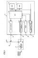
- FIG. 1 shows a structure of a microcomputer 10 according to the first embodiment of this invention.
- the microcomputer 10 is structured to include a drive circuit 11, a sampling/detection circuit 12, a timer 13, a system clock generation circuit 14, a CPU 15, a ROM 16 as an example of a "memory” and a RAM 17.
- a light-receiving device 21 and a P channel type MOS transistor 22 that turns on and off in response to a drive signal from the drive circuit 11 so as to control providing the light-receiving device 21 with a power supply are disposed outside the microcomputer 10.
- Other type of switching device such as a bipolar transistor may be disposed in place of the P channel type MOS transistor 22.
- the light-receiving device 21 receives a remote control signal transmitted from a remote control signal transmitter, and shapes a waveform of the remote control signal that is received.
- the remote control signal transmitted from the remote control signal transmitter includes a burst signal formed of a predetermined carrier frequency.
- the light-receiving device 21 receives the burst signal and shapes the waveform of the signal (including filtering).
- the light-receiving device 21 outputs the waveform-shaped remote control signal as an output signal from its output terminal OUT.
- the remote control signal is an infrared radiation signal
- the light-receiving device 21 is an infrared radiation receiving device.
- the remote control signal is a radio wave signal
- the light-receiving device 21 is a radio wave receiving device.
- the drive circuit 11 outputs the drive signal to a terminal P1.
- the drive signal is applied to a gate of the P channel type MOS transistor 22 through the terminal P1.
- a source of the P channel type MOS transistor 22 is provided with a power supply electric potential VDD (+5 V, for example) that is common to the microcomputer 10, and its drain is connected to a power supply terminal of the light-receiving device 21.
- the P channel type MOS transistor 22 is turned on and the light-receiving device 21 is provided with the power supply electric potential VDD through the P channel type MOS transistor 22, so that the light-receiving device 21 is put into an operation state.
- the P channel type MOS transistor When the drive signal is at a high level, on the other hand, the P channel type MOS transistor is turned off and providing the light-receiving device 21 with the power supply electric potential VDD is stopped, so that the light-receiving device 21 is put into a halt state. That is, when the drive signal alternates between the low level and the high level, the light-receiving device 21 operates intermittently in response to the drive signal. By doing so, it is made possible that the power consumption of the light-receiving device 21 is reduced.
- the sampling/detection circuit 12 samples the output signal (waveform-shaped remote control signal) outputted from the output terminal OUT of the light-receiving device 21 in response to a sampling signal, and detects sampled output signal of the light-receiving device 21.
- the timer 13 counts the time based on a low frequency (32 KHz, for example) clock inputted from a terminal P3.
- the low frequency clock can be generated using a quartz resonator, for example.
- the system clock generation circuit 14 generates a system clock based on a high frequency (10 KHz, for example) clock inputted from a terminal P4.
- the system clock is fed to the drive circuit 11, the sampling/detection circuit 12, the CPU 15, the ROM 16, the RAM 17 and other primary circuits in order to make them operate.
- the high frequency clock may be generated by an oscillation circuit disposed inside the microcomputer 10.
- the CPU 15 controls whole the system, that is, the drive circuit 11, the sampling/detection circuit 12, the timer 13, the system clock generation circuit 14, the ROM 16, the RAM 17 and the like according to the program stored in the ROM 16. In particular, the CPU 15 puts the microcomputer 10 into a standby state in order to reduce the power consumption.
- the system clock generation circuit 14 starts its operation in response to a timer signal telling that the timer 13 completed counting the predetermined period of time. With that, feeding the system clock is restarted and the microcomputer 10 is released from the standby state.
- the P channel type MOS transistor 22 may be disposed inside the microcomputer 10, as shown in Fig. 2 .
- the drive signal from the drive circuit 11 is directly applied to the gate of the P channel type MOS transistor 22, and the drain of the P channel type MOS transistor 22 is connected to the power supply terminal of the light-receiving device 21 through the terminal P1.
- the CPU 15 controls the operations of the microcomputer 10 according to the program stored in the ROM 16.
- the remote control signal first transmitted from the remote control signal transmitter includes a guide pulse (a kind of start pulse) and a data pulse train that is made of a predetermined number of bits (8 bits, for example) and is transmitted subsequent to the guide pulse.
- the guide pulse is a kind of start signal to foretell coming of the data pulse train, while the data pulse train includes commands for controlling the electronic equipment.
- the light-receiving device 21 makes the intermittent operation to alternate between the operation state and the halt state.
- the microcomputer 10 alternates between the operation state and the standby state. With this, the power consumption of the whole system including the light-receiving device 21 and the microcomputer 10 is reduced.
- An interval of the intermittent operation is 500 ⁇ sec, for example.
- the terminal P1 is set to the high level by the drive signal from the drive circuit 11 in a step S1 shown in Fig. 4 . Since the P channel type MOS transistor 22 is turned off as a result, providing the light-receiving device 21 with the power supply electric potential VDD is stopped and the light-receiving device 21 is put into the halt state.
- the microcomputer 10 is put into the standby state described above in order to reduce the power consumption.
- the timer 13 counts the predetermined period of time. The microcomputer 10 is released from the standby state when the timer 13 completes counting the predetermined period time (step S4).
- step S5 the terminal P1 is set to the low level by the drive signal from the drive circuit 11. Since the P channel type MOS transistor 22 is turned on as a result, providing the light-receiving device 21 with the power supply electric potential VDD is started. With this, the light-receiving device 21 is put into a state in which the remote control signal can be received. And it becomes possible that the remote control signal from the light-receiving device 21 is inputted to the terminal P2 of the microcomputer 10 (step S6).
- the sampling/detection circuit 12 detects whether there is the guide pulse in the remote control signal outputted from the output terminal OUT of the light-receiving device 21, in response to the sampling signal generated while the light-receiving device 21 is in operation.
- the guide pulse means a negative polarity pulse varying from the high level to the low level outputted from the light-receiving device 21. It is noted that the guide pulse could be a positive polarity pulse varying from the low level to the high level when the logic levels would be reversed.
- the sequence returns to the step S1. That is, the steps S1 through S7 are repeated as long as the guide pulse is not detected.
- the sequence advances to a next step S8.
- the light-receiving device 21 and the microcomputer 10 are in the operation state in the step S8.
- the data pulse train is outputted from the light-receiving device 21 subsequently to the guide pulse, and sequentially detected by the sampling/detection circuit 12.
- the CPU 15 decodes the data pulse train according to the program stored in the ROM 16, that is, interprets the remote control signal.
- a subsequent step S9 the CPU 15 executes remote control processing, that is, controlling the electronic equipment (power-on, changing the channel or controlling the volume of the TV, for example) based on the result of the decoding.
- remote control processing that is, controlling the electronic equipment (power-on, changing the channel or controlling the volume of the TV, for example) based on the result of the decoding.
- the detection of the guide pulse that is, the detection of the low level of the guide pulse is repeated a plurality of times (5-6 times, for example) in the step S7. That is because there is a possibility that a noise pulse is mistakenly detected as the guide pulse with a single detection, since the guide pulse is usually a single pulse.
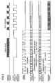
- the intermittent operation of the light-receiving device 21 and the microcomputer 10 is repeated a plurality of times, as shown in Fig. 3 .
- a loop of the steps S1-S7 is repeated a plurality of times after the guide pulse is detected in the step S7 for the first time.
- the CPU 15 judges that the guide pulse has arrived really, and lets the sequence advance from the step S7 to the step S8.
- the sampling/detection circuit 12 After providing the light-receiving device 21 with the power supply electric potential VDD is started in the step S5, it takes a predetermined length of time depending on characteristics of the light-receiving device 21 before the light-receiving device 21 becomes ready to receive the remote control signal. Therefore, when the sampling signal that is generated in the step S7 is generated before the light-receiving device 21 becomes ready to receive the remote control signal, the sampling/detection circuit 12 cannot detect the guide pulse in the remote control signal.
- the CPU 15 is able to adjust the timing to generate the sampling signal so that the sampling signal is generated after the light-receiving device 21 becomes ready to receive the remote control signal in order to make the detection of the guide pulse possible.
- a frequency of the sampling signal in the step S8 is higher than that in the intermittent operation in order to detect the plurality of data pulses sequentially.
- the power consumption of the light-receiving device 21 can be reduced while the power consumption of the microcomputer 10 that controls the light-receiving device 21 is reduced.
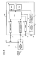
- FIG. 5 shows a structure of a microcomputer 10A according to the second embodiment of this invention.
- the light-receiving device 21 and the microcomputer 10 perform intermittent operation in the remote control signal waiting state.
- the CPU 15 lets only the light-receiving device 21 perform the intermittent operation. That is, the microcomputer 10A is kept in a slow operation state instead of alternating between the standby state and the operation state. After the guide pulse is detected, the microcomputer 10A is put into a fast operation state.
- a consumption current of the light-receiving device 21 is 2-3 mA in many cases, a consumption current of the microcomputer 10A in the slow operation state (frequency of the system clock is 32 KHz, for example) is about 50 ⁇ A which is negligibly small compared with the consumption current of the light-receiving device 21.
- the microcomputer 10A After the guide pulse is detected, the microcomputer 10A is put into the fast operation state (frequency of the system clock is 10MHz, for example) in order to perform the detection of the data pulses and the remote control processing at a high speed. At that time, the consumption current of the microcomputer 10A is about 5 mA.
- the power consumption of the whole system including the light-receiving device 21 and the microcomputer 10A can be reduced sufficiently even when the microcomputer 10A is not put into the standby state.
- the microcomputer 10A has a clock switching circuit 18 in addition to the structure of the microcomputer 10 according to the first embodiment in order to realize the operations described above.
- the clock switching circuit 18 is controlled by the CPU 15 so as to provide the system clock generation circuit 14 with the low frequency clock (32 KHz, for example) inputted from the terminal P3 in the remote control signal waiting state (in the slow operation state).
- the clock switching circuit 18 provides the system clock generation circuit 14 with the high frequency clock (10 MHz, for example) inputted from the terminal P4 after the guide pulse is detected (in the fast operation state).
- the low frequency clock is inputted to the timer 13 as in the first embodiment.
- the P channel type MOS transistor 22 may be disposed inside the microcomputer 10A.
- the CPU 15 controls the operations of the microcomputer 10A according to the program stored in the ROM 16.
- the remote control signal first transmitted from the remote control signal transmitter includes the guide pulse (a kind of start pulse) and the data pulse train that is made of a predetermined number of bits (8 bits, for example) and is transmitted subsequent to the guide pulse.
- step S1 the terminal P1 is set to the high level by the drive signal from the drive circuit 11. Since the P channel type MOS transistor 22 is turned off as a result, providing the light-receiving device 21 with the power supply electric potential VDD is stopped and the light-receiving device 21 is put into the halt state.
- the timer 13 counts the predetermined period of time.
- the terminal P1 is set to the low level by the drive signal from the drive circuit 11 (step S4). Since the P channel type MOS transistor 22 is turned on as a result, providing the light-receiving device 21 with the power supply electric potential VDD is started and the light-receiving device 21 is put into the operation state. With this, it becomes possible that the remote control signal from the light-receiving device 21 is inputted to the terminal P2 (step S5).
- a subsequent step S6 the sampling/detection circuit 12 detects whether there is the guide pulse in the remote control signal outputted from the output terminal OUT of the light-receiving device 21, in response to the sampling signal generated while the light-receiving device 21 is in operation.
- the sequence returns to the step S1. That is, the steps S1 through S6 are repeated as long as the guide pulse is not detected.
- step S6 When the guide pulse is detected in the step S6, the sequence advances to a next step S7.
- the microcomputer 10A is switched into the fast operation state in the step S7.
- a plurality of the data pulses is outputted from the light-receiving device 21 subsequently to the guide pulse, and sequentially detected by the sampling/detection circuit 12.
- the CPU 15 decodes the data pulse train according to the program stored in the ROM 16, that is, interprets the remote control signal.
- a subsequent step S9 the CPU 15 executes remote control processing, that is, controlling the electronic equipment (power-on, changing the channel or controlling the volume of the TV, for example) based on the result of the decoding.
- remote control processing that is, controlling the electronic equipment (power-on, changing the channel or controlling the volume of the TV, for example) based on the result of the decoding.
- the detection of the guide pulse is repeated a plurality of times in the step S6 as in the first embodiment. That is because there is a possibility that a noise pulse is mistakenly detected as the guide pulse with a single detection, since the guide pulse is usually a single pulse.
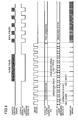
- the intermittent operation of the light-receiving device 21 is repeated a plurality of times, as shown in Fig. 6 .
- a loop of the steps S1-S6 is repeated a plurality of times after the guide pulse is detected (that is, the low level is detected) in the step S6 for the first time.
- the sequence is advanced from the step S6 to the step S7.
- the CPU 15 is able to adjust the timing to generate the sampling signal so that the sampling signal is generated after the light-receiving device 21 becomes ready to receive the remote control signal in order to make the detection of the guide pulse possible in the step S6.
- the power consumption of the light-receiving device can be reduced while the power consumption of the microcomputer that controls the light-receiving device is reduced.
Landscapes
- Engineering & Computer Science (AREA)
- Theoretical Computer Science (AREA)
- Physics & Mathematics (AREA)
- General Engineering & Computer Science (AREA)
- General Physics & Mathematics (AREA)
- Selective Calling Equipment (AREA)
- Details Of Television Systems (AREA)
- Microcomputers (AREA)
- Power Sources (AREA)
- Photometry And Measurement Of Optical Pulse Characteristics (AREA)
Abstract
Description
- This invention relates to a microcomputer controlling a light-receiving device that receives a remote control signal from a remote control signal transmitter.
- Remote-controllable electronic equipment such as a TV, a home stereo system or an air conditioner contains a receiving circuit for a remote control signal. In general, the remote control signal is received by a light-receiving device, the received remote control signal is waveform-shaped, and the waveform-shaped remote control signal is decoded, so that the remote control signal is interpreted.
- This kind of electronic equipment is disclosed in Japanese Patent Application Publication No.
2003-87195 - Although the conventional receiving circuit for the remote control signal samples the remote control signal from the light-receiving device at predetermined intervals, there is a problem of a large amount of power consumption, particularly power consumption by the light-receiving device which is always in operation.
- The object of this invention is directed to reducing the power consumption by the light-receiving device as well as reducing the power consumption by the microcomputer that controls the light-receiving device.
- The solution resides in the features of the independent claims and preferably in those of the dependent claims.
- The invention provides a microcomputer that includes a memory storing a program and a drive circuit driving a switching device. The switching device provides a light-receiving device with a power supply, and the light-receiving device receives a remote control signal. The microcomputer also includes a CPU executing the program stored in the memory. The CPU is configured to switch off, through the drive circuit, the switching device so that the light-receiving device is not provided with the power supply, to set the microcomputer in a standby state for a predetermined period of time and to switch on, through the drive circuit, the switching device so that the light-receiving device is provided with the power supply when the microcomputer is released from the standby state.
- The invention also provides a microcomputer that includes a memory storing a program, a CPU executing the program stored in the memory and a drive circuit driving a switching device. The switching device provides a light-receiving device with a power supply, and the light-receiving device receives a remote control signal. The remote control signal comprises a guide pulse that is transmitted first from a remote control signal transmitter and a data pulse train that is transmitted subsequent to the guide pulse. The CPU is configured to set the microcomputer in a slow operation state and to switch off, through the drive circuit, the switching device so that the light-receiving device is not provided with the power supply for a predetermined period of time and to switch on after the predetermined period of time, through the drive circuit, the switching device so that the light-receiving device is provided with the power supply. The CPU is also configured to switch the microcomputer from the slow operation state to a fast operation state and to decode the data pulse train according to the program stored in the memory when the guide pulse is detected in the remote control signal inputted from the light-receiving device.
-
-
Fig. 1 shows a structure of a microcomputer according to a first embodiment of this invention. -
Fig. 2 shows a structure of the microcomputer according to the first embodiment of this invention. -
Fig. 3 is a timing chart showing an example of operations of the microcomputer according to the first embodiment of this invention. -
Fig. 4 is a flow chart showing a sequence of the example of operations of the microcomputer according to the first embodiment of this invention. -
Fig. 5 shows a structure of a microcomputer according to a second embodiment of this invention. -
Fig. 6 is a timing chart showing an example of operations of the microcomputer according to the second embodiment of this invention. -
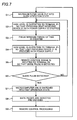
Fig. 7 is a flow chart showing a sequence of the example of operations of the microcomputer according to the second embodiment of this invention. - A first embodiment of this invention is described referring to the drawings.
Fig. 1 shows a structure of amicrocomputer 10 according to the first embodiment of this invention. - The
microcomputer 10 is structured to include adrive circuit 11, a sampling/detection circuit 12, atimer 13, a systemclock generation circuit 14, aCPU 15, aROM 16 as an example of a "memory" and aRAM 17. - A light-receiving
device 21 and a P channel type MOS transistor 22 (an example of "switching device") that turns on and off in response to a drive signal from thedrive circuit 11 so as to control providing the light-receivingdevice 21 with a power supply are disposed outside themicrocomputer 10. Other type of switching device such as a bipolar transistor may be disposed in place of the P channeltype MOS transistor 22. - The light-receiving
device 21 receives a remote control signal transmitted from a remote control signal transmitter, and shapes a waveform of the remote control signal that is received. In this case, the remote control signal transmitted from the remote control signal transmitter includes a burst signal formed of a predetermined carrier frequency. The light-receivingdevice 21 receives the burst signal and shapes the waveform of the signal (including filtering). - The light-
receiving device 21 outputs the waveform-shaped remote control signal as an output signal from its output terminal OUT. In the case where the remote control signal is an infrared radiation signal, the light-receivingdevice 21 is an infrared radiation receiving device. Or, in the case where the remote control signal is a radio wave signal, the light-receivingdevice 21 is a radio wave receiving device. - To describe the structure of the
microcomputer 10, thedrive circuit 11 outputs the drive signal to a terminal P1. The drive signal is applied to a gate of the P channeltype MOS transistor 22 through the terminal P1. A source of the P channeltype MOS transistor 22 is provided with a power supply electric potential VDD (+5 V, for example) that is common to themicrocomputer 10, and its drain is connected to a power supply terminal of the light-receivingdevice 21. - As a result, when the drive signal is at a low level, the P channel
type MOS transistor 22 is turned on and the light-receivingdevice 21 is provided with the power supply electric potential VDD through the P channeltype MOS transistor 22, so that the light-receivingdevice 21 is put into an operation state. - When the drive signal is at a high level, on the other hand, the P channel type MOS transistor is turned off and providing the light-receiving
device 21 with the power supply electric potential VDD is stopped, so that the light-receivingdevice 21 is put into a halt state. That is, when the drive signal alternates between the low level and the high level, the light-receiving device 21 operates intermittently in response to the drive signal. By doing so, it is made possible that the power consumption of the light-receivingdevice 21 is reduced. - The sampling/
detection circuit 12 samples the output signal (waveform-shaped remote control signal) outputted from the output terminal OUT of the light-receiving device 21 in response to a sampling signal, and detects sampled output signal of the light-receivingdevice 21. - The
timer 13 counts the time based on a low frequency (32 KHz, for example) clock inputted from a terminal P3. The low frequency clock can be generated using a quartz resonator, for example. - The system
clock generation circuit 14 generates a system clock based on a high frequency (10 KHz, for example) clock inputted from a terminal P4. The system clock is fed to thedrive circuit 11, the sampling/detection circuit 12, theCPU 15, theROM 16, theRAM 17 and other primary circuits in order to make them operate. The high frequency clock may be generated by an oscillation circuit disposed inside themicrocomputer 10. - The
CPU 15 controls whole the system, that is, thedrive circuit 11, the sampling/detection circuit 12, thetimer 13, the systemclock generation circuit 14, theROM 16, theRAM 17 and the like according to the program stored in theROM 16. In particular, theCPU 15 puts themicrocomputer 10 into a standby state in order to reduce the power consumption. - In the standby state, only the
timer 13 is in operation and all the other circuits halt their operations. That is, feeding the system clock is stopped in the standby state by halting the operation of the systemclock generation circuit 14. - In the circuits to which feeding the system clock is stopped, logic states of inputs and outputs of logic gates (AND circuit, NOR circuit, inverter circuit and the like) constituting the circuits are fixed at either "1" or "0". As a result, in the standby state, only a leakage current flows and the power consumption is reduced in the circuits to which feeding the system clock is stopped. These circuits are often formed of CMOS. The standby state lasts for a predetermined period of time that is set in the
timer 13. - The system
clock generation circuit 14 starts its operation in response to a timer signal telling that thetimer 13 completed counting the predetermined period of time. With that, feeding the system clock is restarted and themicrocomputer 10 is released from the standby state. - The P channel
type MOS transistor 22 may be disposed inside themicrocomputer 10, as shown inFig. 2 . In this case, the drive signal from thedrive circuit 11 is directly applied to the gate of the P channeltype MOS transistor 22, and the drain of the P channeltype MOS transistor 22 is connected to the power supply terminal of the light-receiving device 21 through the terminal P1. - Next, an example sequence of operations of the
microcomputer 10 according to the first embodiment is explained referring toFig. 3 andFig. 4 . TheCPU 15 controls the operations of themicrocomputer 10 according to the program stored in theROM 16. The remote control signal first transmitted from the remote control signal transmitter includes a guide pulse (a kind of start pulse) and a data pulse train that is made of a predetermined number of bits (8 bits, for example) and is transmitted subsequent to the guide pulse. The guide pulse is a kind of start signal to foretell coming of the data pulse train, while the data pulse train includes commands for controlling the electronic equipment. - First, in a remote control signal waiting state, the light-receiving
device 21 makes the intermittent operation to alternate between the operation state and the halt state. In synchronization with it, themicrocomputer 10 alternates between the operation state and the standby state. With this, the power consumption of the whole system including the light-receivingdevice 21 and themicrocomputer 10 is reduced. An interval of the intermittent operation is 500 µsec, for example. - The terminal P1 is set to the high level by the drive signal from the
drive circuit 11 in a step S1 shown inFig. 4 . Since the P channeltype MOS transistor 22 is turned off as a result, providing the light-receivingdevice 21 with the power supply electric potential VDD is stopped and the light-receivingdevice 21 is put into the halt state. In a subsequent step S2, themicrocomputer 10 is put into the standby state described above in order to reduce the power consumption. In a subsequent step S3, thetimer 13 counts the predetermined period of time. Themicrocomputer 10 is released from the standby state when thetimer 13 completes counting the predetermined period time (step S4). - In a subsequent step S5, the terminal P1 is set to the low level by the drive signal from the
drive circuit 11. Since the P channeltype MOS transistor 22 is turned on as a result, providing the light-receivingdevice 21 with the power supply electric potential VDD is started. With this, the light-receivingdevice 21 is put into a state in which the remote control signal can be received. And it becomes possible that the remote control signal from the light-receivingdevice 21 is inputted to the terminal P2 of the microcomputer 10 (step S6). - In a subsequent step S7, the sampling/
detection circuit 12 detects whether there is the guide pulse in the remote control signal outputted from the output terminal OUT of the light-receivingdevice 21, in response to the sampling signal generated while the light-receivingdevice 21 is in operation. In this case, the guide pulse means a negative polarity pulse varying from the high level to the low level outputted from the light-receivingdevice 21. It is noted that the guide pulse could be a positive polarity pulse varying from the low level to the high level when the logic levels would be reversed. When the guide pulse is not detected, the sequence returns to the step S1. That is, the steps S1 through S7 are repeated as long as the guide pulse is not detected. - When the guide pulse is detected in the step S7, the sequence advances to a next step S8. The light-receiving
device 21 and themicrocomputer 10 are in the operation state in the step S8. In the step S8, the data pulse train is outputted from the light-receivingdevice 21 subsequently to the guide pulse, and sequentially detected by the sampling/detection circuit 12. - The
CPU 15 decodes the data pulse train according to the program stored in theROM 16, that is, interprets the remote control signal. - In a subsequent step S9, the
CPU 15 executes remote control processing, that is, controlling the electronic equipment (power-on, changing the channel or controlling the volume of the TV, for example) based on the result of the decoding. When the remote control processing in the step S9 is completed, the sequence returns to the step S1, that is, the state waiting for the next remote control signal. - It is preferable for prevention of malfunctioning that the detection of the guide pulse, that is, the detection of the low level of the guide pulse is repeated a plurality of times (5-6 times, for example) in the step S7. That is because there is a possibility that a noise pulse is mistakenly detected as the guide pulse with a single detection, since the guide pulse is usually a single pulse.
- In this case, the intermittent operation of the light-receiving
device 21 and themicrocomputer 10 is repeated a plurality of times, as shown inFig. 3 . To describe the case referring to the flow chart shown inFig. 4 , a loop of the steps S1-S7 is repeated a plurality of times after the guide pulse is detected in the step S7 for the first time. - When the guide pulse is always detected in the plurality of detections that follow, the
CPU 15 judges that the guide pulse has arrived really, and lets the sequence advance from the step S7 to the step S8. - After providing the light-receiving
device 21 with the power supply electric potential VDD is started in the step S5, it takes a predetermined length of time depending on characteristics of the light-receivingdevice 21 before the light-receivingdevice 21 becomes ready to receive the remote control signal. Therefore, when the sampling signal that is generated in the step S7 is generated before the light-receivingdevice 21 becomes ready to receive the remote control signal, the sampling/detection circuit 12 cannot detect the guide pulse in the remote control signal. - Thus, it is preferable that the
CPU 15 is able to adjust the timing to generate the sampling signal so that the sampling signal is generated after the light-receivingdevice 21 becomes ready to receive the remote control signal in order to make the detection of the guide pulse possible. - Also, it is preferable that a frequency of the sampling signal in the step S8 is higher than that in the intermittent operation in order to detect the plurality of data pulses sequentially.
- According to the first embodiment, as described above, the power consumption of the light-receiving
device 21 can be reduced while the power consumption of themicrocomputer 10 that controls the light-receivingdevice 21 is reduced. - A second embodiment of this invention is described referring to the drawings.
Fig. 5 shows a structure of amicrocomputer 10A according to the second embodiment of this invention. In the first embodiment, the light-receivingdevice 21 and themicrocomputer 10 perform intermittent operation in the remote control signal waiting state. - In the second embodiment, on the other hand, the
CPU 15 lets only the light-receivingdevice 21 perform the intermittent operation. That is, themicrocomputer 10A is kept in a slow operation state instead of alternating between the standby state and the operation state. After the guide pulse is detected, themicrocomputer 10A is put into a fast operation state. - While a consumption current of the light-receiving
device 21 is 2-3 mA in many cases, a consumption current of themicrocomputer 10A in the slow operation state (frequency of the system clock is 32 KHz, for example) is about 50 µA which is negligibly small compared with the consumption current of the light-receivingdevice 21. - After the guide pulse is detected, the
microcomputer 10A is put into the fast operation state (frequency of the system clock is 10MHz, for example) in order to perform the detection of the data pulses and the remote control processing at a high speed. At that time, the consumption current of themicrocomputer 10A is about 5 mA. - Therefore, the power consumption of the whole system including the light-receiving
device 21 and themicrocomputer 10A can be reduced sufficiently even when themicrocomputer 10A is not put into the standby state. - The
microcomputer 10A has aclock switching circuit 18 in addition to the structure of themicrocomputer 10 according to the first embodiment in order to realize the operations described above. Theclock switching circuit 18 is controlled by theCPU 15 so as to provide the systemclock generation circuit 14 with the low frequency clock (32 KHz, for example) inputted from the terminal P3 in the remote control signal waiting state (in the slow operation state). - And the
clock switching circuit 18 provides the systemclock generation circuit 14 with the high frequency clock (10 MHz, for example) inputted from the terminal P4 after the guide pulse is detected (in the fast operation state). The low frequency clock is inputted to thetimer 13 as in the first embodiment. - In the second embodiment also, the P channel
type MOS transistor 22 may be disposed inside themicrocomputer 10A. - Next, an example sequence of operations of the
microcomputer 10A according to the second embodiment is described referring toFig. 6 andFig. 7 . TheCPU 15 controls the operations of themicrocomputer 10A according to the program stored in theROM 16. The remote control signal first transmitted from the remote control signal transmitter includes the guide pulse (a kind of start pulse) and the data pulse train that is made of a predetermined number of bits (8 bits, for example) and is transmitted subsequent to the guide pulse. - First, in the remote control signal waiting state, the
microcomputer 10A is put into the slow operation state (step S1). In a subsequent step S2, the terminal P1 is set to the high level by the drive signal from thedrive circuit 11. Since the P channeltype MOS transistor 22 is turned off as a result, providing the light-receivingdevice 21 with the power supply electric potential VDD is stopped and the light-receivingdevice 21 is put into the halt state. - In a subsequent step S3, the
timer 13 counts the predetermined period of time. When thetimer 13 completes counting the predetermined period of time, the terminal P1 is set to the low level by the drive signal from the drive circuit 11 (step S4). Since the P channeltype MOS transistor 22 is turned on as a result, providing the light-receivingdevice 21 with the power supply electric potential VDD is started and the light-receivingdevice 21 is put into the operation state. With this, it becomes possible that the remote control signal from the light-receivingdevice 21 is inputted to the terminal P2 (step S5). - In a subsequent step S6, the sampling/
detection circuit 12 detects whether there is the guide pulse in the remote control signal outputted from the output terminal OUT of the light-receivingdevice 21, in response to the sampling signal generated while the light-receivingdevice 21 is in operation. When the guide pulse is not detected, the sequence returns to the step S1. That is, the steps S1 through S6 are repeated as long as the guide pulse is not detected. - When the guide pulse is detected in the step S6, the sequence advances to a next step S7. The
microcomputer 10A is switched into the fast operation state in the step S7. - In a subsequent step S8, a plurality of the data pulses is outputted from the light-receiving
device 21 subsequently to the guide pulse, and sequentially detected by the sampling/detection circuit 12. TheCPU 15 decodes the data pulse train according to the program stored in theROM 16, that is, interprets the remote control signal. - In a subsequent step S9, the
CPU 15 executes remote control processing, that is, controlling the electronic equipment (power-on, changing the channel or controlling the volume of the TV, for example) based on the result of the decoding. When the remote control processing in the step S9 is completed, the sequence returns to the step S1, that is, the state waiting for the next remote control signal. - It is preferable for prevention of malfunctioning that the detection of the guide pulse is repeated a plurality of times in the step S6 as in the first embodiment. That is because there is a possibility that a noise pulse is mistakenly detected as the guide pulse with a single detection, since the guide pulse is usually a single pulse.
- In this case, the intermittent operation of the light-receiving
device 21 is repeated a plurality of times, as shown inFig. 6 . To describe the case referring to the flow chart shown inFig. 7 , a loop of the steps S1-S6 is repeated a plurality of times after the guide pulse is detected (that is, the low level is detected) in the step S6 for the first time. When the guide pulse is always detected in the plurality of detections that follow, the sequence is advanced from the step S6 to the step S7. - Also, it is preferable in the second embodiment as in the first embodiment that the
CPU 15 is able to adjust the timing to generate the sampling signal so that the sampling signal is generated after the light-receivingdevice 21 becomes ready to receive the remote control signal in order to make the detection of the guide pulse possible in the step S6. - According to the embodiments of this invention, the power consumption of the light-receiving device can be reduced while the power consumption of the microcomputer that controls the light-receiving device is reduced.
Claims (7)
- A microcomputer comprising:a memory (16) storing a program;a drive circuit (11) driving a switching device (22), the switching device (22) providing a light-receiving device (21) with a power supply, the light-receiving device (21) receiving a remote control signal; anda CPU (15) executing the program stored in the memory (16), the CPU (15) being configured to switch off, through the drive circuit (11), the switching device (22) so that the light-receiving device (21) is not provided with the power supply, to set the microcomputer (10) in a standby state for a predetermined period of time and to switch on, through the drive circuit (11), the switching device (22) so that the light-receiving device (21) is provided with the power supply when the microcomputer (10) is released from the standby state.
- The microcomputer of claim 1, wherein the remote control signal comprises a guide pulse that is transmitted first from a remote control signal transmitter and a data pulse train that is transmitted subsequent to the guide pulse, and the CPU (15) decodes the data pulse train according to the program stored in the memory (16) when the guide pulse is detected in the remote control signal inputted from the light-receiving device (21) after the switching device (22) is switched on so that the light-receiving device (21) is provided with the power supply.
- The microcomputer of claim 2, wherein the CPU (15) switches off the switching device (22) and sets the microcomputer (10) in the standby state when the guide pulse is not detected in the remote control signal inputted from the light-receiving device (21).
- The microcomputer of any of claims 1 to 3, wherein the switching device (22) is disposed inside the microcomputer (10).
- The microcomputer of any of claims 1 to 4, wherein the CPU (15) is further configured to set the microcomputer (10A) in a slow operation state and to switch the microcomputer (10A) from the slow operation state to a fast operation state and to decode the data pulse train according to the program stored in the memory (16) when the guide pulse is detected in the remote control signal inputted from the light-receiving device (21).
- A microcomputer comprising:a memory (16) storing a program;a CPU(15) executing the program stored in the memory (16); anda drive circuit (11) driving a switching device (22), the switching device (22) providing a light-receiving device (21) with a power supply, the light-receiving device (21) receiving a remote control signal,wherein the remote control signal comprises a guide pulse that is transmitted first from a remote control signal transmitter and a data pulse train that is transmitted subsequent to the guide pulse,the CPU (15) is configured to set the microcomputer (10A) in a slow operation state and to switch off, through the drive circuit (11), the switching device (22) so that the light-receiving device (21) is not provided with the power supply for a predetermined period of time and to switch on after the predetermined period of time, through the drive circuit (11), the switching device (22) so that the light-receiving device (21) is provided with the power supply, andthe CPU (15) is also configured to switch the microcomputer (10A) from the slow operation state to a fast operation state and to decode the data pulse train according to the program stored in the memory (16) when the guide pulse is detected in the remote control signal inputted from the light-receiving device (21).
- The microcomputer of claim 6, wherein the CPU (15) switches off the switching device (22) when the guide pulse is not detected in the remote control signal inputted from the light-receiving device (21).
Applications Claiming Priority (1)
| Application Number | Priority Date | Filing Date | Title |
|---|---|---|---|
| JP2009232465A JP2011082745A (en) | 2009-10-06 | 2009-10-06 | Microcomputer |
Publications (2)
| Publication Number | Publication Date |
|---|---|
| EP2309364A2 true EP2309364A2 (en) | 2011-04-13 |
| EP2309364A3 EP2309364A3 (en) | 2012-05-09 |
Family
ID=43446301
Family Applications (1)
| Application Number | Title | Priority Date | Filing Date |
|---|---|---|---|
| EP10013387A Withdrawn EP2309364A3 (en) | 2009-10-06 | 2010-10-06 | Microcomputer |
Country Status (4)
| Country | Link |
|---|---|
| US (1) | US8217714B2 (en) |
| EP (1) | EP2309364A3 (en) |
| JP (1) | JP2011082745A (en) |
| CN (1) | CN102033597B (en) |
Families Citing this family (5)
| Publication number | Priority date | Publication date | Assignee | Title |
|---|---|---|---|---|
| JP5358338B2 (en) * | 2009-08-06 | 2013-12-04 | セミコンダクター・コンポーネンツ・インダストリーズ・リミテッド・ライアビリティ・カンパニー | Remote control signal receiving circuit |
| JP5576754B2 (en) * | 2010-09-29 | 2014-08-20 | キヤノン株式会社 | Radiation imaging device |
| JP2013082391A (en) * | 2011-10-12 | 2013-05-09 | Autonetworks Technologies Ltd | Vehicle ecu |
| JP5672229B2 (en) * | 2011-12-26 | 2015-02-18 | 株式会社デンソー | Battery monitoring device |
| KR102674531B1 (en) * | 2016-09-28 | 2024-06-13 | 엘지전자 주식회사 | Electronic Equipment and Control Method for the same |
Citations (1)
| Publication number | Priority date | Publication date | Assignee | Title |
|---|---|---|---|---|
| JP2003087195A (en) | 2001-09-11 | 2003-03-20 | Sanyo Electric Co Ltd | Electronics |
Family Cites Families (10)
| Publication number | Priority date | Publication date | Assignee | Title |
|---|---|---|---|---|
| JPH0775426B2 (en) * | 1986-07-23 | 1995-08-09 | アルプス電気株式会社 | Communication device |
| JP3403765B2 (en) * | 1993-09-13 | 2003-05-06 | 株式会社アルファ | Remote control device |
| JP3392751B2 (en) * | 1998-01-30 | 2003-03-31 | 三洋電機株式会社 | Remote control device |
| JP2001095073A (en) * | 1999-09-22 | 2001-04-06 | Funai Electric Co Ltd | Remote control transmitter and electrical equipment controlled by the remote control transmitter |
| JP3994615B2 (en) * | 2000-03-15 | 2007-10-24 | ソニー株式会社 | Remote control receiving apparatus and method |
| US6993393B2 (en) * | 2001-12-19 | 2006-01-31 | Cardiac Pacemakers, Inc. | Telemetry duty cycle management system for an implantable medical device |
| JP3557198B2 (en) * | 2002-06-17 | 2004-08-25 | 株式会社東芝 | Switching power supply circuit and electronic equipment |
| JP4484528B2 (en) * | 2004-01-06 | 2010-06-16 | パナソニック株式会社 | Low power consumption device |
| JP4541018B2 (en) * | 2004-04-01 | 2010-09-08 | 株式会社日立製作所 | DIGITAL BROADCAST RECEIVING DEVICE, TV DEVICE, AND DIGITAL BROADCAST RECEIVING METHOD |
| JP5358338B2 (en) * | 2009-08-06 | 2013-12-04 | セミコンダクター・コンポーネンツ・インダストリーズ・リミテッド・ライアビリティ・カンパニー | Remote control signal receiving circuit |
-
2009
- 2009-10-06 JP JP2009232465A patent/JP2011082745A/en not_active Ceased
-
2010
- 2010-09-23 US US12/888,693 patent/US8217714B2/en active Active
- 2010-09-27 CN CN201010296781.5A patent/CN102033597B/en not_active Expired - Fee Related
- 2010-10-06 EP EP10013387A patent/EP2309364A3/en not_active Withdrawn
Patent Citations (1)
| Publication number | Priority date | Publication date | Assignee | Title |
|---|---|---|---|---|
| JP2003087195A (en) | 2001-09-11 | 2003-03-20 | Sanyo Electric Co Ltd | Electronics |
Also Published As
| Publication number | Publication date |
|---|---|
| JP2011082745A (en) | 2011-04-21 |
| US8217714B2 (en) | 2012-07-10 |
| US20110080210A1 (en) | 2011-04-07 |
| CN102033597A (en) | 2011-04-27 |
| CN102033597B (en) | 2014-03-12 |
| EP2309364A3 (en) | 2012-05-09 |
Similar Documents
| Publication | Publication Date | Title |
|---|---|---|
| US8217714B2 (en) | Microcomputer including remote controlled light-receiving device with power supply switch | |
| US20100156505A1 (en) | Circuit arrangement and method for generating a drive signal for a transistor | |
| US10050585B2 (en) | Ultra-low power crystal oscillator with adaptive self-start | |
| US20110254722A1 (en) | Remote control signal receiver and electrical apparatus | |
| JP2018092631A (en) | Low power consumption signal receiving circuit and power saving method of signal receiving system | |
| KR100403096B1 (en) | Remote control receiver and method of controlling the same | |
| US20080055099A1 (en) | Wake-up controller and a method therefor for power control over peripheral circuitry based upon slots of a data field | |
| JP3392751B2 (en) | Remote control device | |
| EP3333680B1 (en) | Drive unit, method and circuit for touch control drive electrode, and touch control display panel | |
| EP2750261A1 (en) | Electronic Device and Control Method Thereof | |
| US20060146970A1 (en) | Start-stop synchronization serial communication circuit and semiconductor integrated circuit having start-stop synchronization serial communication circuit | |
| JP5358338B2 (en) | Remote control signal receiving circuit | |
| US20170075853A1 (en) | Universal serial bus device, electronic apparatus including the same, and control method thereof | |
| CN109936354B (en) | Startup and shutdown circuit | |
| CN1143188C (en) | Electronic watch and data transmission method of the electronic watch | |
| JP2002135856A (en) | Remote control device | |
| US20060022661A1 (en) | Circuit arrangement for a microcontroller and method of operating a remote control receiver | |
| JP4640040B2 (en) | Wireless transmission device | |
| JP2004004138A5 (en) | ||
| JP2015061103A (en) | Pulse reception circuit | |
| CN108233799B (en) | Circuit for controlling output of DC motor to stabilize FG signal | |
| JP3760744B2 (en) | Constant voltage output device | |
| JP3906769B2 (en) | Communication device | |
| JPH10126396A (en) | Integrated circuit | |
| JPH05308682A (en) | Remote control signal receiving device |
Legal Events
| Date | Code | Title | Description |
|---|---|---|---|
| PUAI | Public reference made under article 153(3) epc to a published international application that has entered the european phase |
Free format text: ORIGINAL CODE: 0009012 |
|
| AK | Designated contracting states |
Kind code of ref document: A2 Designated state(s): AL AT BE BG CH CY CZ DE DK EE ES FI FR GB GR HR HU IE IS IT LI LT LU LV MC MK MT NL NO PL PT RO RS SE SI SK SM TR |
|
| AX | Request for extension of the european patent |
Extension state: BA ME |
|
| PUAL | Search report despatched |
Free format text: ORIGINAL CODE: 0009013 |
|
| AK | Designated contracting states |
Kind code of ref document: A3 Designated state(s): AL AT BE BG CH CY CZ DE DK EE ES FI FR GB GR HR HU IE IS IT LI LT LU LV MC MK MT NL NO PL PT RO RS SE SI SK SM TR |
|
| AX | Request for extension of the european patent |
Extension state: BA ME |
|
| RIC1 | Information provided on ipc code assigned before grant |
Ipc: G06F 1/32 20060101AFI20120403BHEP |
|
| 17P | Request for examination filed |
Effective date: 20120926 |
|
| 17Q | First examination report despatched |
Effective date: 20130516 |
|
| GRAP | Despatch of communication of intention to grant a patent |
Free format text: ORIGINAL CODE: EPIDOSNIGR1 |
|
| INTG | Intention to grant announced |
Effective date: 20140314 |
|
| RAP1 | Party data changed (applicant data changed or rights of an application transferred) |
Owner name: SANYO SEMICONDUCTOR CO., LTD. Owner name: SANYO ELECTRIC CO., LTD. |
|
| STAA | Information on the status of an ep patent application or granted ep patent |
Free format text: STATUS: THE APPLICATION IS DEEMED TO BE WITHDRAWN |
|
| 18D | Application deemed to be withdrawn |
Effective date: 20140725 |