EP2309305A1 - Apparatus for generating spatially modulated light and image recording apparatus - Google Patents
Apparatus for generating spatially modulated light and image recording apparatus Download PDFInfo
- Publication number
- EP2309305A1 EP2309305A1 EP10177154A EP10177154A EP2309305A1 EP 2309305 A1 EP2309305 A1 EP 2309305A1 EP 10177154 A EP10177154 A EP 10177154A EP 10177154 A EP10177154 A EP 10177154A EP 2309305 A1 EP2309305 A1 EP 2309305A1
- Authority
- EP
- European Patent Office
- Prior art keywords
- light
- light modulator
- reflective surfaces
- moving
- optical system
- Prior art date
- Legal status (The legal status is an assumption and is not a legal conclusion. Google has not performed a legal analysis and makes no representation as to the accuracy of the status listed.)
- Granted
Links
Images




Classifications
-
- G—PHYSICS
- G02—OPTICS
- G02B—OPTICAL ELEMENTS, SYSTEMS OR APPARATUS
- G02B26/00—Optical devices or arrangements for the control of light using movable or deformable optical elements
- G02B26/08—Optical devices or arrangements for the control of light using movable or deformable optical elements for controlling the direction of light
- G02B26/0808—Optical devices or arrangements for the control of light using movable or deformable optical elements for controlling the direction of light by means of one or more diffracting elements
-
- B—PERFORMING OPERATIONS; TRANSPORTING
- B41—PRINTING; LINING MACHINES; TYPEWRITERS; STAMPS
- B41J—TYPEWRITERS; SELECTIVE PRINTING MECHANISMS, i.e. MECHANISMS PRINTING OTHERWISE THAN FROM A FORME; CORRECTION OF TYPOGRAPHICAL ERRORS
- B41J19/00—Character- or line-spacing mechanisms
- B41J19/16—Special spacing mechanisms for circular, spiral, or diagonal-printing apparatus
-
- G—PHYSICS
- G02—OPTICS
- G02B—OPTICAL ELEMENTS, SYSTEMS OR APPARATUS
- G02B27/00—Optical systems or apparatus not provided for by any of the groups G02B1/00 - G02B26/00, G02B30/00
- G02B27/42—Diffraction optics, i.e. systems including a diffractive element being designed for providing a diffractive effect
- G02B27/46—Systems using spatial filters
-
- H—ELECTRICITY
- H04—ELECTRIC COMMUNICATION TECHNIQUE
- H04N—PICTORIAL COMMUNICATION, e.g. TELEVISION
- H04N9/00—Details of colour television systems
- H04N9/12—Picture reproducers
- H04N9/31—Projection devices for colour picture display, e.g. using electronic spatial light modulators [ESLM]
- H04N9/3129—Projection devices for colour picture display, e.g. using electronic spatial light modulators [ESLM] scanning a light beam on the display screen
- H04N9/3132—Projection devices for colour picture display, e.g. using electronic spatial light modulators [ESLM] scanning a light beam on the display screen using one-dimensional electronic spatial light modulators
-
- H—ELECTRICITY
- H04—ELECTRIC COMMUNICATION TECHNIQUE
- H04N—PICTORIAL COMMUNICATION, e.g. TELEVISION
- H04N9/00—Details of colour television systems
- H04N9/12—Picture reproducers
- H04N9/31—Projection devices for colour picture display, e.g. using electronic spatial light modulators [ESLM]
- H04N9/3141—Constructional details thereof
- H04N9/315—Modulator illumination systems
Definitions
- the present invention relates to a technique for generating a spatially modulated light with using a spatial light modulator of diffraction grating type.
- a light modulator element of diffraction grating type which is capable of changing the depth of grating by alternately forming fixed ribbons and moving ribbons on a substrate with a semiconductor device manufacturing technique and sagging the moving ribbons relatively to the fixed ribbons.
- a diffraction grating light amounts of regularly reflected light and diffracted light are changed by changing the depth of grooves.
- An apparatus for generating a spatially modulated light comprises a laser light source, a spatial light modulator having a plurality of light modulator elements which are arranged in an element arrangement direction, and an illumination optical system for generating a linear illumination light from a light emitted from the laser light source, the linear illumination light being directed onto the plurality of light modulator elements.
- Each light modulator element of the plurality of light modulator elements has strip-like moving reflective surfaces and strip-like fixed reflective surfaces which are elongated in a direction perpendicular to the element arrangement direction and are alternately arranged in the element arrangement direction.
- the moving reflective surfaces are sagged in a state where both end portions of the moving reflective surfaces are supported, and each light modulator element changes between a state of emitting a zeroth order light and a state of emitting first order diffracted lights, to generate a group of signal lights, each of which is a zeroth order light or first order diffracted lights, from the plurality of light modulator elements, as a spatially modulated light.
- the illumination optical system comprises a first optical system, a slit member, and a second optical system in this order.
- the first optical system forms an intermediate image of the laser light source at an intermediate image position between the laser light source and the spatial light modulator, the intermediate image being formed with respect to a vertical direction which is a direction perpendicular to a horizontal direction corresponding to the element arrangement direction and perpendicular to an optical axis, the intermediate image being long in the horizontal direction.
- the slit member is positioned at the intermediate image position and has a slit extending in the horizontal direction, the slit member blocking an undesired light which appears on both sides or one side of the intermediate image in the vertical direction.
- the second optical system reforms the intermediate image onto the spatial light modulator with respect to at least the vertical direction with using a light passing through the slit, to generate the linear illumination light.
- the undesired light of the intermediate image is blocked by the slit member to thereby acquire a spatially modulated light with high contrast. Since a beam width relative to each light modulator element in the direction perpendicular to the element arrangement direction is limited, the form of the beam is made uniform and the linear illumination light with high quality is acquired to thereby obtain a recorded image with high quality.
- the present invention is also intended for an image recording apparatus for recording an image on a recording material.
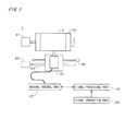
- Fig. 1 is a view showing an image recording apparatus
- Fig. 1 is a views showing a constitution of an image recording apparatus 1 in accordance with a preferred embodiment of the present invention.
- the image recording apparatus 1 has an optical head 10 which is an apparatus for generating a spatially modulated light and a holding drum 70 for holding a recording material 9 on its outer surface.
- a spatially modulated light from the optical head 10 is relatively moved while the light is applied (irradiated) onto the recording material 9 to record an image on the recording material 9 (i.e., an image is recorded by light irradiation).
- the recording material 9 used are a printing plate, a film for forming the printing plate and the like, for example.
- a photosensitive drum for plateless printing may be used as the holding drum 70 and in this case, it is understood that the recording material 9 corresponds to a surface of the photosensitive drum and the holding drum 70 holds the recording material 9 as a unit.
- the holding drum 70 is rotated about a central axis of its cylindrical surface by a motor 81 and the optical head 10 thereby travels relatively to the recording material 9 at a constant speed in a main scan direction.
- the main scan direction is a direction crossing an arrangement direction of positions irradiated with light from a plurality of light modulator elements later discussed.
- the optical head 10 is movable by a motor 82 and a ball screw 83 in parallel to a rotation axis of the holding drum 70 in a sub scan direction, and the position of the optical head 10 is detected by an encoder 84.
- a moving mechanism including the motors 81 and 82 and the ball screw 83 moves the outer surface of the holding drum 70 and the recording material 9 relatively to the optical head 10 (and the light from the special light modulator) at a constant speed in the main scan direction and also, the scanning mechanism moves them relatively to the optical head 10 in the sub scan direction, crossing the main scan direction.
- the motors 81 and 82, the encoder 84, and the optical head 10 are connected to a general control part 21, which controls the motors 81 and 82 and emission of light from the spatial light modulator in the optical head 10 to record an image on the recording material 9 held on the holding drum 70 by light.
- Data of an image to be recorded on the recording material 9 is prepared in a signal generation part 23 in advance, and a signal processing part 22 receives an image signal outputted from the signal generation part 23 on the basis of a control signal from the general control part 21.
- the signal processing part 22 converts the image signal into a signal for the optical head 10 to input the signal to the general control part 21, and then a voltage representing the image signal is applied to each light modulator element of the spatial light modulator by control of the general control part 21.
- Figs. 2 and 3 are a plan view and a side view each showing the optical head 10 which is expanded along the optical axis.
- Figs. 2 and 3 are not the accurate plan view and side view, in which three-dimensional arrangement of optical elements are ignored.
- the optical head 10 has a laser light source 11, an illumination optical system 12, a spatial light modulator 13, and an image forming optical system 14 in this order from the left of Figs. 2 and 3 .
- a laser light emitted from the laser light source 11 is converted into a linear illumination light in the illumination optical system 12 and directed to the spatial light modulator 13.
- a light which is spatially modulated by the spatial light modulator 13 is directed to the recording material 9 through the image forming optical system 14.
- the laser light source 11 is a semiconductor laser, and may be one semiconductor laser or a plurality of semiconductor lasers. In the case of the plurality of semiconductor lasers, laser lights emitted from them are superimposed.
- the laser light source 11 may be a semiconductor laser having a plurality of light emitting points arranged in a vertical direction of Fig. 2 .
- the illumination optical system can be used a homogenizing optical system in which an array lens disclosed in Japanese Patent Application Laid-Open No. 2002-72132 is used as a homogenizer.
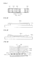
- Fig. 4 is an enlarged view of a plurality of light modulator elements 131 in the spatial light modulator 13.
- the light modulator elements 131 are arranged in one direction (hereinafter, referred to as "element arrangement direction") in the spatial light modulator 13.
- a section of the linear illumination, light has a linear shape which is long in the element arrangement direction, and the linear illumination light is directed onto the plurality of light modulator elements 131.
- Each light modulator element 131 is a diffraction grating whose grating depth is changeable, and it is manufactured with the semiconductor device manufacturing technique.
- each light modulator element 131 a plurality of moving ribbons 131a and a plurality of fixed ribbons 131b are alternately arranged in parallel in the element arrangement direction, and each of the ribbons 131a, 131b has a strip shape which is elongated in a direction perpendicular to the element arrangement direction.
- the moving ribbons 131a are vertically movable relatively to a base surface therebehind, and the fixed ribbons 131b are fixed with respect to the base surface.
- the light modulator element with diffraction grating structure for example, the GLV (Grating Light Valve) (trademarked by Sillicon Light Machine, Sunnyvale, California) is well known.
- Figs. 5A and 5B are side views of the moving ribbons 131a as viewer from the element arrangement direction.
- the upper surface of the moving ribbon 131a is a strip-like moving reflective surface which is parallel to a base surface 131c (i.e., the upper surface of a substrate) and is elongated in the direction perpendicular to the element arrangement direction.
- Fig. 5A shows an initial state where the moving ribbons 131a are not sagged
- Fig. 5B shows a state where a voltage (electric potential difference) is applied between the moving ribbons 131a and the base surface 131c and the moving ribbons 131a are sagged toward the base surface 131c by electrostatic force. Both end portions of the moving ribbons 131a are supported, and center portions of the moving ribbons 131a are made closer to the base surface 131 by sagging.
- the fixed ribbon 131b has the same structure as the moving ribbon 131a shown in Fig. 5A .
- the upper surface of the fixed ribbon 131b is a strip-like fixed reflective surface which is parallel to the base surface 131c (i.e., the upper surface of the substrate) and is elongated in the direction perpendicular to the element arrangement direction.
- the fixed ribbons 131b do not sag.
- Figs. 6A and 6B are views each showing a cross section of the light modulator element 131 which is cut by a plane perpendicular to the moving ribbons 131a and the fixed ribbons 131b.
- the moving ribbon 131a and the fixed ribbon 131b have the approximately same width, and the moving ribbons 131a and the fixed ribbons 131b are arranged at regular pitches.
- the height of a moving reflective surface 132a from the base surface 131c is equal to that of a fixed reflective surface 132b from the base surface 131c.
- a zeroth order diffracted light (which is a normally reflected light, and hereinafter referred to as a "zeroth order light") L2 with the maximum light amount (i.e., the maximum intensity) is outputted from the light modulator element 131 by reflection of an incident light L1.
- Fig. 6B is a view showing a state where the moving ribbons 131a are sagged and a difference d of the heights between the moving reflective surfaces 132a and the fixed reflective surfaces 132b is ((2n-1)/4) ⁇ ( ⁇ is a wavelength of an incident light and n is a positive integer).
- a light amount (light intensity) of (+/-) first order diffracted lights L3 (further, high odd-order diffracted lights) outputted from the light modulator element 131 is maximum, and a light amount of the zeroth order light is minimum.
- Figs. 6A and 6B show a state where the incident light L1 enters perpendicularly to the base surface 131c, however, the incident light actually tilts along a plane which is perpendicular to the base surface 131c and parallel to the direction of extending the ribbons.
- First order diffracted lights are emitted in a case where the difference between an optical path through the moving reflective surfaces 132a and an optical path through the fixed reflective surfaces 132b fulfills ((2n-1)/2) ⁇ . Therefore, in the case of incident angle ⁇ , the difference of heights between the reflective surfaces 132a and 132b is ((2n-1)/4) ⁇ cos ⁇ . This is also applied to the case of Fig. 9B which is discussed later.
- the height of the fixed reflective surfaces 132b from the base surface 131c is almost equal to that of the moving reflective surfaces 132a from the base surface 131c in the state where moving ribbons 131a are not sagged.
- the height of the moving reflective surfaces 132a from the base surfaces 121c is changed by sagging the moving ribbons 131a in accordance with an inputted voltage, to change the light modulator element 121 between the state of emitting the zeroth order light and that of emitting the first order diffracted lights.
- the moving ribbons 131a are slightly sagged so that light amounts of zeroth order lights from all the light modulator elements 131 are accurately equal in a state where each light modulator element 131 emits a zeroth order light.
- the illumination optical system 12 has a slit member 125, and an optical system between the slit member 125 and the laser light source 11 l is hereinafter referred to as a "first optical system 12a" and an optical system between the slit member 125 and the spatial light modulator i is referred to as a "second optical system 12b".
- the first optical system 12a has a collimating lens 121, a lens 122, a fly-eye lens 123, and a cylindrical lens 124 in this order from the laser light source 11.
- a laser light emitted from the laser light source 11 is collimated in the vertical direction of Fig. 3 by the collimating lens 121, and a collimated light is directed to the lens 122.
- the light is made parallel with respect to the vertical direction of Fig. 2 (hereinafter, referred to as "horizontal direction") by the lens 122, and is converged in the vertical direction of Fig. 3 .
- the "horizontal direction'' is a direction which is perpendicular to the optical axis J1 and corresponds to the arrangement direction of the light modulator elements 131, and the "vertical direction” is a direction which is perpendicular to both of the optical axis J1 and the horizontal direction.
- the vertical direction here is not required to correspond to the direction of gravity.
- the light passing through the lens 122 is divided into five segments in the horizontal direction by the fly-eye lens 123, where the light is parallel with respect to the vertical direction, and the light is converged in the vertical direction by the cylindrical lens 124.
- the slit member 125 has a slit 125a which is a horizontally long opening, and the light from the cylindrical lens 124 is most converged at the position of the slit 125a.
- an intermediate image position is provided between the laser light source 11 and the spatial light modulator 1.3 in the illumination optical system 12, and the slit member 125 is positioned at the intermediate image position.
- An intermediate image of the laser light source 11 is formed at the position of the slit 125a. Formation of the intermediate image is only in the vertical direction, and the intermediate image is made elongated in the horizontal direction by the fly-eye lens 123.
- the second optical system 12b has a lens 126 and a cylindrical lens 127 in this order from the slit member 125.
- the light divided in the horizontal direction by the fly-eye lens 123 passes through the slit 125a and is accurately superimposed in the horizontal direction at the position of the spatial light modulator 13 by the lens 126, to make a distribution of light amount (i.e., a distribution of light intensity) uniform.
- the intermediate image is reformed at the position of the spatial light modulator 13 by the lens 126 and the cylindrical lens 127, to thereby generate a linear illumination light. Reformation of the intermediate image may be performed only in the vertical direction.
- the image forming optical system 14 has a lens 141, a light blocking member 142, and a lens 143 in this order from the spatial light modulator 13.
- the lens 141 is provided with a function for forming a far-field image (a distribution in angle) of the spatial light modulator 13 at the light blocking member 142.
- the light from each light modulator element 131 is separated into a zeroth order light, first order lights, and high order lights at the light blocking member 142.
- a center clearance 142a of the light blocking member 142 is designed to pass only the zeroth order light, and the zeroth order light emitted from each light modulator element 131 in the spatial light modulator 13 passes through the center clearance 142a of the light blocking member 142 by the lens 141 to be directed to the recording material 9 through the lens 143.
- an image (actually, dot) of the light modulator element 131 is formed on the recording material 9.
- the first order diffracted lights from the light modulator element 131 are directed to the light blocking member 142 by the lens 141 and blocked there.
- a spatially modulated light which is a group of zeroth order lights is directed to the recording material 9, and a group of images (actually, dots) of the light modulator elements 131 are written on the recording material 9.
- the state of emitting the zeroth order light is an ON state where writing is performed on the recording material 9, and the state of emitting the first order diffracted lights is an OFF state where writing is not performed on the recording material 9.
- the zeroth order light is a signal light for recordation of an image.
- Fig. 7 is a graph showing a a light intensity (reflection intensity) distribution of a zeroth order light from a light modulator element 131 in a state where the first order diffracted lights are emitted.
- the vertical axis in Fig. 7 represents position on the light modulator element 131 in the direction of the ribbons, and 0 represents the optical axis J1 or a center position in the vertical direction on the light modulator element 131.
- the horizontal axis represents the light intensity distribution (reflection intensity distribution) in a direction where the zeroth order light is diffracted (reflected) in a case where a light is uniformly irradiated onto the whole of the light modulator element 131.
- a light intensity of the zeroth order light is increased in the vicinities of both end portions of the moving ribbons 131a and the fixed ribbons 131b in the light modulator element 131.
- emission of the zeroth order light is fully suppressed in a certain range in the center of the moving ribbons 131a and the fixed ribbons 131b, while the first order diffracted lights are emitted.
- This phenomenon occurs because an amount of sagging of the vicinities of the both end portions of the moving ribbons 131a is smaller than that of the center portions thereof and the center portions are sagged in a state almost parallel to the base surface 131c, as shown in Fig.
- an area of the moving ribbons 131a where an amounts of sagging is constant is referred to as an "effective area”.
- the range of the vertical axis is 200 ⁇ m, and the width of the effective area is 70 ⁇ m.
- the vertical width of the linear illumination light irradiated to the spatial light modulator 13 is out of range of the width of the effective area, the zeroth order light emitted from an area outside the effective area is directed to the recording material 9 even if the light modulator elements 131 are in the OFF state. This results in deterioration in contrast (i.e., an ON/OFF ratio which is an extinction ratio of a signal light).
- the collimating lens 121 also called as a FAC (Fast Axis Collimator) lens
- FAC Fast Axis Collimator
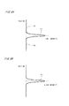
- Fig. 8A is a graph showing a light intensity distribution at the position of the slit 125a in a case where an optical system is adjusted at practical cost.
- the vertical axis represents position in the vertical direction and the horizontal axis represents light intensity.
- side lobes 62 appear on the both sides of a main lobe 61 (i.e., on the both sides of the main lobe 61 in the vertical direction) because of influence of the first optimal system 12a.
- the first optical system 12a there may be a case where a side lobe appears on only one side of the main lobe, and yet another case where an undesired light which doesn't have a bump form like the side lobe, but slightly broadens from the main lobe appears.
- an undesired light which doesn't have a bump form like the side lobe, but slightly broadens from the main lobe appears.
- such various undesired lights other than those appear in the main portion of the main lobe are collectively called as an "undesired light", and lights corresponding to the main lobe are referred to as a "main beam”.
- the slit 125a is provided within a range of the main beam in order to block the undesired light.
- the light including only the main lobe 61, i.e., the main beam is directed to the second optical system 12b as shown in Fig. 8B . and the linear illumination light without the undesired light is irradiated to the spatial light modulator 13. Consequently, it is possible to prevent the undesired light from being irradiated to areas other than the effective areas of the light modulator elements 131 in the OFF state and to prevent decrease in contrast of the signal lights. That is, a spatially modulated light with high quality is generated in the spatial light modulator 13.
- the linear illumination light which is suitable for the spatial light modulator of diffraction grating type can be generated without expensive optical elements in the optical head 10, which is an apparatus for generating the spatially modulated light, to achieve high performance at low cost. Also, since a beam width relative to each light modulator element in the direction perpendicular to the element arrangement direction is limited, the form of the beam is made uniform and the linear illumination light with high quality is acquired to thereby obtain a recorded image with high quality.
- the optical head 10 including the slit member 125 is especially suitable for recording an image on the recording material 9 with less reciprocity failure.
- the fly-eye lens 123 which is a part of optical elements (the fly-eye lens 123 and the lens 126) for making the distribution of light amount uniform in the horizontal direction is not provided in the second optical system 12b but in the first optical system 12a, the light from the complicated first optical system 12a is directed to the slit 125a to simplify the second optical system 12b. As a result, it is possible to suppress decrease in quality of the linear illumination light by the second optical system 12b.
- All the optical elements for making the distribution of light amount uniform in the horizontal direction may be provided in the first optical system 12a.
- other homogenizer such as a DOE element (a diffractive optical element) or a rod lens can be used.
- the laser light source 11 and the first optical system 12a and the slit member 125 of the illumination optical system 12 are fixed on a holding member 151. Actually, these optical parts are supported by various supporting members provided on the holding member 151.
- the second optical system 12b, the spatial light modulator 13, and the image forming optical system 14 are attached on a large-sized base 152 which is placed on a base part of the image recording apparatus 1, as appropriate, with interposing a supporting member.
- the position of the holding member 151 is easily determined to the base 152 (i.e., to the second optical system 12b), being easily attachable and detachable by screws or the like.
- the laser light source 11, the first optical system 12a, and the slit member 125 are attachable to and detachable from other portions including the second optical system 12b as a unit which is fixed on the holding member 151.
- adjustment or change of optical parts from the light source to the portions for forming the intermediate image can be easily performed by detaching these parts.
- exchanging parts since these optical parts are easily detached and exchanged, it is possible to easily maintain a state where no deterioration in contrast or the like occurs.
- the optical axis J1 is bent at the position of the spatial light modulator 13 and the like, so the form and arrangement of the base 152 are different from that shown in Fig. 3 .
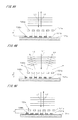
- Figs. 9A and 9B are another example of the light modulator element 131, showing cross sections corresponding to Figs. 6A and 6B , respectively.
- the upper surface of the moving ribbons 131a are the strip-like moving reflective surfaces 132a which are parallel to the base surface 131c and elongated in the direction perpendicular to the element arrangement direction.
- the fixed ribbons 131b are fixed on the base surface 131c, and their upper surfaces are the strip-like fixed reflective surfaces 132b which are parallel to the base surface 131c and elongated in the direction perpendicular to the element arrangement direction.
- Fig. 9A shows a state where moving ribbons 131a are not sagged (the moving ribbons 131a may be slightly sagged).
- a difference d of the heights between the moving reflective surfaces 132a and the fixed reflective surfaces 132b is (2n/4) ⁇ , and a light amount of the zeroth order light L2 from the light modulator clement 131 is maximum, and a light amount of the first order diffracted lights is minimum.
- the difference d of heights is (2n/4) ⁇ cos ⁇ (the same is applied to Fig. 9C ).
- Fig. 9B shows a state where a voltage (electric potential difference) is applied between the moving ribbons 131a and the base surface 131c and the moving ribbons 131a are sagged toward the base surface 131c by electrostatic force.
- the moving ribbons 131 a are sagged, and a difference d of the heights between the moving reflective surfaces 132a and the fixed reflective surfaces 132b is ((2n+1)/4) ⁇ .
- the (+/-) first order diffracted lights L3 with the maximum light amount (and further high-order diffracted lights) are outputted from the light modulator element 131.
- the zeroth order light is emitted in a state where sagging of the moving reflective surfaces 132a doesn't exist (or is small) and the first order diffracted lights are emitted in a state where sagging of the moving reflective surfaces 132a is large.
- the moving reflective surfaces 132a and the fixed reflective surfaces 132b are positioned at different heights from the base surfaces 131c in a state where the signal light, i.e., the zeroth order light, is emitted.
- the signal light i.e., the zeroth order light
- the slit 125a is provided and the linear illumination light without the undesired light is irradiated to the spatial light modulator 13.
- the slit 125a is provided and the linear illumination light without the undesired light is irradiated to the spatial light modulator 13.
- a light modulator element which emits the first order diffracted lights L3 shown in Fig. 9B in a state where moving ribbons 131a are not sagged or the moving ribbons 131a are slightly sagged.
- the zeroth order light L2 is emitted in a state where the moving ribbons 131a are further sagged as shown in Fig. 9C .
- a difference d of heights between the reflective surfaces 132a and 132b is ((2n-1)/4) ⁇ in the state of Fig. 9B
- the difference d is (2n/4) ⁇ in the state of Fig. 9C .
- the first order diffracted lights may serve as the signal lights for writing in the image recording apparatus 1.
- the moving reflective surfaces 132a and the fixed reflective surfaces 132b are positioned at different heights from the base surface 131 c in a state where the signal light is emitted.
- a light blocking member for blocking the zeroth order lights on the optical axis J1 to pass the first order diffracted lights which travel to a direction apart from the optical axis J1 is provided instead of the light blocking member 142 of Fig. 2 .
- a group of (+/-) first order diffracted lights is collected on the recording material 9 as a spatially modulated light, by a large lens behind the light blocking member.
- the moving ribbons 131a are sagged in the state of emitting the zeroth order light, when all the elements are irradiated in the state of emitting the zeroth order light, a distribution of light intensity of the first order diffracted lights in the vertical direction is according to that illustrated in Fig. 7 . Therefore, in a case where writing is performed with the light modulator elements 131 shown in Figs. 9B and 9C in which the first order diffracted lights serve as the signal light, an undesired light is blocked by the slit member 125 to thereby acquire the signal light with high contrast at low cost, as illustrated in Figs. 8A and 8B .
- a light modulator element 131 in which an amount of sagging of the moving reflective surfaces 132a in a state where a signal light is emitted is smaller than that in a state where no signal light is emitted, removal of undesired light from the illumination light greatly contributes to improvement of contrast of the signal light.
- the moving reflective surfaces 132a are made slightly sagged for adjustment of light amount even in a state where the signal light is emitted, as discussed earlier. Therefore, also in a light modulator element 131 emitting a signal light in a state where all amount of sagging of the moving reflective surfaces 132a is large (a light modulator element emitting a non-signal light in Fig. 9A and emitting a signal light in Fig.
- Fig. 10 is a perspective view showing another example of the image recording apparatus.
- a control unit 20 in an image recording apparatus 1a is provided with a general control part 21, a signal processing part 22, and a signal generation part 23 of Fig. 1 .
- the image recording apparatus 1a is an apparatus for recording an image of a pattern such as mask or conductive wire on a glass substrate 9a for manufacturing a glass mask, a TFT (Thin Film Transistor) liquid crystal panel or the like, and it is a so-called direct writing apparatus for directly writing an image by irradiation with light.
- the glass substrate 9a coated with a photosensitive material is a recording material for recording information of an image.
- the image recording apparatus 1a has a table 72 for holding the glass substrate 9a on its surface on the (+Z) side and a table moving mechanism 85 for moving the table 72 in the Y direction (main scan direction) is fixed on a base part 74.
- a position detecting module 85a for detecting position of the table 72 is provided on the base part 74.
- An optical head 10 for emitting light toward the glass substrate 9a is located above the table 72 and the optical head 10 is movably supported by a head moving mechanism 86 in the X direction which is the sub scan direction. That is to say, the main scan direction and the sub scan direction are parallel to the horizontal table 72, and the table moving mechanism 85 and the head moving mechanism 86 function as a mechanism for moving the table 72 relatively to the optical head 10 including a spatial light modulator at a constant speed in the main scan direction and also moving the table 72 relatively to the optical head 10 in the sub scan direction perpendicular to the main scan direction.
- a frame 75 is attached to the base part 74 over the table 72 and the head moving mechanism 86 is fixed on the frame 75.
- the basic structure of the optical head 10 is the same as that shown in Figs. 2 and 3 , and the slit member 125 is provided at the intermediate image position in the illumination optical system 12.
- a film of photosensitive material (i.e., resist) to be photosensed by irradiation with ultraviolet rays is previously formed on the main surface of the glass substrate 9a on the (+Z) side in this preferred embodiment.
- the arrangement direction of the plurality of light modulator elements 131 see Fig.
- the arrangement direction of the plurality of light modulator elements 131 do not necessarily have to correspond to the sub scan direction only if the arrangement direction is a direction crossing the main scan direction which is the Y direction.
- the main scan direction which is the moving direction of the glass substrate 9a has only to be a direction crossing the arrangement direction of positions irradiated with light, similarly to the case of Fig. 1 .
- the table 72 is moved relatively to the optical head 10 in the (-Y) direction by the table moving mechanism 85 and irradiation positions of light from the optical head 10 are thereby continuously moved relatively to the glass substrate 9a in the (+Y) direction (i.e., main scanning is performed).
- emission of signal lights is performed in synchronization with a signal outputted from the position detecting module 85a.
- writing is performed on a strip-like region (swath), extending in the Y direction, with a width corresponding to the size of image of spots of the spatial light modulator.
- the optical head 10 moves in the sub scan direction (X direction) by a distance corresponding to a width of the strip-like region in the X direction, the moving direction of the table 72 is reversed, and then writing in a backward path of the table 72 is performed on a new strip-like region in contact with the side of the strip-like region written in a forward path. Then, the optical head 10 intermittently moves in the X direction while reciprocally moving the table 72 in the Y direction, to record an image on the whole writing area of the plane glass substrate 9a in the image recording apparatus 1a.
- the slit member 125 is provided at the intermediate image position in the illumination optical system 12, it is possible to achieve improvement of contrast of the signal lights at low cost. As a result, a quality of an image to be recorded can be easily enhanced.
- the moving ribbons 131a and the fixed ribbons 131b are not limited to a ribbon shape in a strict meaning.
- the fixed ribbons 131b may be bock-shaped portions whose upper surfaces are fixed reflective surfaces.
- the laser light source 11 is not limited to a semiconductor laser but may be a gas laser, a solid laser, or the like.
- the recording material 9 and the glass substrate 9a can be moved by other technique only if they are movable relatively to the optical head 10.
- the recording material may be material coated with photosensitive material such as a printed circuit board or a semiconductor substrate, other material with photosensitivity, or material which responds to heat by light irradiation.
Landscapes
- Physics & Mathematics (AREA)
- Optics & Photonics (AREA)
- General Physics & Mathematics (AREA)
- Engineering & Computer Science (AREA)
- Multimedia (AREA)
- Signal Processing (AREA)
- Exposure And Positioning Against Photoresist Photosensitive Materials (AREA)
- Mechanical Light Control Or Optical Switches (AREA)
- Facsimile Scanning Arrangements (AREA)
Abstract
Description
- The present invention relates to a technique for generating a spatially modulated light with using a spatial light modulator of diffraction grating type.
- Developed has been a light modulator element of diffraction grating type which is capable of changing the depth of grating by alternately forming fixed ribbons and moving ribbons on a substrate with a semiconductor device manufacturing technique and sagging the moving ribbons relatively to the fixed ribbons. In such a diffraction grating, light amounts of regularly reflected light and diffracted light are changed by changing the depth of grooves. It is proposed that, in Japanese Patent Application Laid-Open No.
2004-4525 2002-72132 3,522,133 - Meanwhile, since the moving ribbons are sagged in a state where their both end portions are supported, an amount of sagging of the both end portions becomes smaller than that of other portions of the moving ribbons. Therefore, if light is incident on the both end portions, light modulation by the light modulator element is failed to cause decrease in contrast or the like. To solve this problem, a linear illumination light with a very narrow width has to be accurately irradiated along the center of the line where the light modulator elements are arranged. Generation of such linear illumination light from a laser light requires expensive lenses with high quality which should be located in an optical system from a laser light source to light modulator elements, and this increases the manufacturing cost of an image recording apparatus.
- It is a main object of the present invention to generate a linear illumination light which is suitable for a spatial light modulator of diffraction grating type without using expensive optical elements and to provide an apparatus for generating a spatially modulated light with high performance at low cost.
- An apparatus for generating a spatially modulated light according to the invention comprises a laser light source, a spatial light modulator having a plurality of light modulator elements which are arranged in an element arrangement direction, and an illumination optical system for generating a linear illumination light from a light emitted from the laser light source, the linear illumination light being directed onto the plurality of light modulator elements. Each light modulator element of the plurality of light modulator elements has strip-like moving reflective surfaces and strip-like fixed reflective surfaces which are elongated in a direction perpendicular to the element arrangement direction and are alternately arranged in the element arrangement direction. The moving reflective surfaces are sagged in a state where both end portions of the moving reflective surfaces are supported, and each light modulator element changes between a state of emitting a zeroth order light and a state of emitting first order diffracted lights, to generate a group of signal lights, each of which is a zeroth order light or first order diffracted lights, from the plurality of light modulator elements, as a spatially modulated light. The illumination optical system comprises a first optical system, a slit member, and a second optical system in this order. The first optical system forms an intermediate image of the laser light source at an intermediate image position between the laser light source and the spatial light modulator, the intermediate image being formed with respect to a vertical direction which is a direction perpendicular to a horizontal direction corresponding to the element arrangement direction and perpendicular to an optical axis, the intermediate image being long in the horizontal direction. The slit member is positioned at the intermediate image position and has a slit extending in the horizontal direction, the slit member blocking an undesired light which appears on both sides or one side of the intermediate image in the vertical direction. The second optical system reforms the intermediate image onto the spatial light modulator with respect to at least the vertical direction with using a light passing through the slit, to generate the linear illumination light.
- In the invention, the undesired light of the intermediate image is blocked by the slit member to thereby acquire a spatially modulated light with high contrast. Since a beam width relative to each light modulator element in the direction perpendicular to the element arrangement direction is limited, the form of the beam is made uniform and the linear illumination light with high quality is acquired to thereby obtain a recorded image with high quality.
- The present invention is also intended for an image recording apparatus for recording an image on a recording material.
- These and other objects, features, aspects and advantages of the present invention will become more apparent from the following detailed description of the present invention when taken in conjunction with the accompanying drawings.
-
Fig. 1 is a view showing an image recording apparatus; -
Figs. 2 and3 arc a plan view and a side view each showing an optical head which is expanded; -
Fig. 4 is a view showing a spatial light modulator; -
Figs. 5A and 5B are side views of a light modulator element; -
Figs. 6A and6B are cross-sectional views of the light modulator element; -
Fig. 7 is a graph showing a intensity distribution of a zeroth order light emitted from a light modulator element in a state where first order diffracted lights are emitted; -
Fig. 8A is a graph showing a light intensity distribution at a position of a slit; -
Fig. 8B is a graph showing a light intensity distribution after light has passed through the slit; -
Figs. 9A, 9B, and 9C are cross-sectional views each showing another example of the light modulator element; and -
Fig. 10 is a perspective view showing another example of the image recording apparatus. -
Fig. 1 is a views showing a constitution of an image recordingapparatus 1 in accordance with a preferred embodiment of the present invention. Theimage recording apparatus 1 has anoptical head 10 which is an apparatus for generating a spatially modulated light and aholding drum 70 for holding arecording material 9 on its outer surface. A spatially modulated light from theoptical head 10 is relatively moved while the light is applied (irradiated) onto therecording material 9 to record an image on the recording material 9 (i.e., an image is recorded by light irradiation). As therecording material 9, used are a printing plate, a film for forming the printing plate and the like, for example. A photosensitive drum for plateless printing may be used as theholding drum 70 and in this case, it is understood that therecording material 9 corresponds to a surface of the photosensitive drum and theholding drum 70 holds therecording material 9 as a unit. - The
holding drum 70 is rotated about a central axis of its cylindrical surface by amotor 81 and theoptical head 10 thereby travels relatively to therecording material 9 at a constant speed in a main scan direction. The main scan direction is a direction crossing an arrangement direction of positions irradiated with light from a plurality of light modulator elements later discussed. Theoptical head 10 is movable by amotor 82 and aball screw 83 in parallel to a rotation axis of theholding drum 70 in a sub scan direction, and the position of theoptical head 10 is detected by anencoder 84. In other words, a moving mechanism including themotors ball screw 83 moves the outer surface of theholding drum 70 and therecording material 9 relatively to the optical head 10 (and the light from the special light modulator) at a constant speed in the main scan direction and also, the scanning mechanism moves them relatively to theoptical head 10 in the sub scan direction, crossing the main scan direction. - The
motors encoder 84, and theoptical head 10 are connected to ageneral control part 21, which controls themotors optical head 10 to record an image on therecording material 9 held on theholding drum 70 by light. - Data of an image to be recorded on the
recording material 9 is prepared in asignal generation part 23 in advance, and asignal processing part 22 receives an image signal outputted from thesignal generation part 23 on the basis of a control signal from thegeneral control part 21. Thesignal processing part 22 converts the image signal into a signal for theoptical head 10 to input the signal to thegeneral control part 21, and then a voltage representing the image signal is applied to each light modulator element of the spatial light modulator by control of thegeneral control part 21. -
Figs. 2 and3 are a plan view and a side view each showing theoptical head 10 which is expanded along the optical axis.Figs. 2 and3 are not the accurate plan view and side view, in which three-dimensional arrangement of optical elements are ignored. - The
optical head 10 has alaser light source 11, an illuminationoptical system 12, aspatial light modulator 13, and an image formingoptical system 14 in this order from the left ofFigs. 2 and3 . A laser light emitted from thelaser light source 11 is converted into a linear illumination light in the illuminationoptical system 12 and directed to thespatial light modulator 13. A light which is spatially modulated by thespatial light modulator 13 is directed to therecording material 9 through the image formingoptical system 14. Thelaser light source 11 is a semiconductor laser, and may be one semiconductor laser or a plurality of semiconductor lasers. In the case of the plurality of semiconductor lasers, laser lights emitted from them are superimposed. Further, thelaser light source 11 may be a semiconductor laser having a plurality of light emitting points arranged in a vertical direction ofFig. 2 . As the illumination optical system, can be used a homogenizing optical system in which an array lens disclosed inJapanese Patent Application Laid-Open No. 2002-72132 -
Fig. 4 is an enlarged view of a plurality oflight modulator elements 131 in thespatial light modulator 13. Thelight modulator elements 131 are arranged in one direction (hereinafter, referred to as "element arrangement direction") in thespatial light modulator 13. A section of the linear illumination, light has a linear shape which is long in the element arrangement direction, and the linear illumination light is directed onto the plurality oflight modulator elements 131. Eachlight modulator element 131 is a diffraction grating whose grating depth is changeable, and it is manufactured with the semiconductor device manufacturing technique. In eachlight modulator element 131,a plurality of movingribbons 131a and a plurality of fixedribbons 131b are alternately arranged in parallel in the element arrangement direction, and each of theribbons ribbons 131a are vertically movable relatively to a base surface therebehind, and the fixedribbons 131b are fixed with respect to the base surface. As the light modulator element with diffraction grating structure, for example, the GLV (Grating Light Valve) (trademarked by Sillicon Light Machine, Sunnyvale, California) is well known. -
Figs. 5A and 5B are side views of the movingribbons 131a as viewer from the element arrangement direction. The upper surface of the movingribbon 131a is a strip-like moving reflective surface which is parallel to abase surface 131c (i.e., the upper surface of a substrate) and is elongated in the direction perpendicular to the element arrangement direction.Fig. 5A shows an initial state where the movingribbons 131a are not sagged, andFig. 5B shows a state where a voltage (electric potential difference) is applied between the movingribbons 131a and thebase surface 131c and the movingribbons 131a are sagged toward thebase surface 131c by electrostatic force. Both end portions of the movingribbons 131a are supported, and center portions of the movingribbons 131a are made closer to thebase surface 131 by sagging. - The fixed
ribbon 131b has the same structure as the movingribbon 131a shown inFig. 5A . The upper surface of the fixedribbon 131b is a strip-like fixed reflective surface which is parallel to thebase surface 131c (i.e., the upper surface of the substrate) and is elongated in the direction perpendicular to the element arrangement direction. However, the fixedribbons 131b do not sag. -
Figs. 6A and6B are views each showing a cross section of thelight modulator element 131 which is cut by a plane perpendicular to the movingribbons 131a and the fixedribbons 131b. As shown inFig. 6A , the movingribbon 131a and the fixedribbon 131b have the approximately same width, and the movingribbons 131a and the fixedribbons 131b are arranged at regular pitches. In a state where movingribbons 131a are not sagged as shown inFig. 6A , the height of a movingreflective surface 132a from thebase surface 131c is equal to that of a fixedreflective surface 132b from thebase surface 131c. In this state, a zeroth order diffracted light (which is a normally reflected light, and hereinafter referred to as a "zeroth order light") L2 with the maximum light amount (i.e., the maximum intensity) is outputted from thelight modulator element 131 by reflection of an incident light L1. On the other hand,Fig. 6B is a view showing a state where the movingribbons 131a are sagged and a difference d of the heights between the movingreflective surfaces 132a and the fixedreflective surfaces 132b is ((2n-1)/4)λ (λ is a wavelength of an incident light and n is a positive integer). In the state ofFig. 6B . a light amount (light intensity) of (+/-) first order diffracted lights L3 (further, high odd-order diffracted lights) outputted from thelight modulator element 131 is maximum, and a light amount of the zeroth order light is minimum. -
Figs. 6A and6B show a state where the incident light L1 enters perpendicularly to thebase surface 131c, however, the incident light actually tilts along a plane which is perpendicular to thebase surface 131c and parallel to the direction of extending the ribbons. First order diffracted lights are emitted in a case where the difference between an optical path through the movingreflective surfaces 132a and an optical path through the fixedreflective surfaces 132b fulfills ((2n-1)/2) λ. Therefore, in the case of incident angle θ, the difference of heights between thereflective surfaces Fig. 9B which is discussed later. - As discussed above, the height of the fixed
reflective surfaces 132b from thebase surface 131c is almost equal to that of the movingreflective surfaces 132a from thebase surface 131c in the state where movingribbons 131a are not sagged. The height of the movingreflective surfaces 132a from the base surfaces 121c is changed by sagging the movingribbons 131a in accordance with an inputted voltage, to change thelight modulator element 121 between the state of emitting the zeroth order light and that of emitting the first order diffracted lights. Actually, the movingribbons 131a are slightly sagged so that light amounts of zeroth order lights from all thelight modulator elements 131 are accurately equal in a state where eachlight modulator element 131 emits a zeroth order light. - Although a spatially modulated light is generated by reflection of the illumination light in the spatial
light modulator 13, bending of the optical path J1 by reflection of the light on the spatiallight modulator 13 is ignored inFigs. 2 and3 as described above. - The illumination
optical system 12 has aslit member 125, and an optical system between theslit member 125 and the laser light source 11 l is hereinafter referred to as a "firstoptical system 12a" and an optical system between theslit member 125 and the spatial light modulator i is referred to as a "secondoptical system 12b". - The first
optical system 12a has acollimating lens 121, alens 122, a fly-eye lens 123, and acylindrical lens 124 in this order from thelaser light source 11. A laser light emitted from thelaser light source 11 is collimated in the vertical direction ofFig. 3 by thecollimating lens 121, and a collimated light is directed to thelens 122. The light is made parallel with respect to the vertical direction ofFig. 2 (hereinafter, referred to as "horizontal direction") by thelens 122, and is converged in the vertical direction ofFig. 3 . The "horizontal direction'' is a direction which is perpendicular to the optical axis J1 and corresponds to the arrangement direction of thelight modulator elements 131, and the "vertical direction" is a direction which is perpendicular to both of the optical axis J1 and the horizontal direction. The vertical direction here is not required to correspond to the direction of gravity. - The light passing through the
lens 122 is divided into five segments in the horizontal direction by the fly-eye lens 123, where the light is parallel with respect to the vertical direction, and the light is converged in the vertical direction by thecylindrical lens 124. Theslit member 125 has aslit 125a which is a horizontally long opening, and the light from thecylindrical lens 124 is most converged at the position of theslit 125a. In other words, an intermediate image position is provided between thelaser light source 11 and the spatial light modulator 1.3 in the illuminationoptical system 12, and theslit member 125 is positioned at the intermediate image position. An intermediate image of thelaser light source 11 is formed at the position of theslit 125a. Formation of the intermediate image is only in the vertical direction, and the intermediate image is made elongated in the horizontal direction by the fly-eye lens 123. - The second
optical system 12b has alens 126 and acylindrical lens 127 in this order from theslit member 125. The light divided in the horizontal direction by the fly-eye lens 123 passes through theslit 125a and is accurately superimposed in the horizontal direction at the position of the spatiallight modulator 13 by thelens 126, to make a distribution of light amount (i.e., a distribution of light intensity) uniform. With respect to the vertical direction, the intermediate image is reformed at the position of the spatiallight modulator 13 by thelens 126 and thecylindrical lens 127, to thereby generate a linear illumination light. Reformation of the intermediate image may be performed only in the vertical direction. - The image forming
optical system 14 has alens 141, alight blocking member 142, and alens 143 in this order from the spatiallight modulator 13. Thelens 141 is provided with a function for forming a far-field image (a distribution in angle) of the spatiallight modulator 13 at thelight blocking member 142. The light from eachlight modulator element 131 is separated into a zeroth order light, first order lights, and high order lights at thelight blocking member 142. Acenter clearance 142a of thelight blocking member 142 is designed to pass only the zeroth order light, and the zeroth order light emitted from eachlight modulator element 131 in the spatiallight modulator 13 passes through thecenter clearance 142a of thelight blocking member 142 by thelens 141 to be directed to therecording material 9 through thelens 143. With this structure, an image (actually, dot) of thelight modulator element 131 is formed on therecording material 9. On the other hand, the first order diffracted lights from thelight modulator element 131 are directed to thelight blocking member 142 by thelens 141 and blocked there. As a result, a spatially modulated light which is a group of zeroth order lights is directed to therecording material 9, and a group of images (actually, dots) of thelight modulator elements 131 are written on therecording material 9. In thelight modulator element 131, the state of emitting the zeroth order light is an ON state where writing is performed on therecording material 9, and the state of emitting the first order diffracted lights is an OFF state where writing is not performed on therecording material 9. in other words, the zeroth order light is a signal light for recordation of an image. - Next discussion will be made on a function of the
slit member 125.Fig. 7 is a graph showing a a light intensity (reflection intensity) distribution of a zeroth order light from alight modulator element 131 in a state where the first order diffracted lights are emitted. The vertical axis inFig. 7 represents position on thelight modulator element 131 in the direction of the ribbons, and 0 represents the optical axis J1 or a center position in the vertical direction on thelight modulator element 131. The horizontal axis represents the light intensity distribution (reflection intensity distribution) in a direction where the zeroth order light is diffracted (reflected) in a case where a light is uniformly irradiated onto the whole of thelight modulator element 131. As shown inFig. 7 , in the state where the first order diffracted lights are emitted, a light intensity of the zeroth order light is increased in the vicinities of both end portions of the movingribbons 131a and the fixedribbons 131b in thelight modulator element 131. Conversely, emission of the zeroth order light is fully suppressed in a certain range in the center of the movingribbons 131a and the fixedribbons 131b, while the first order diffracted lights are emitted. This phenomenon occurs because an amount of sagging of the vicinities of the both end portions of the movingribbons 131a is smaller than that of the center portions thereof and the center portions are sagged in a state almost parallel to thebase surface 131c, as shown inFig. 5 . In the following description, an area of the movingribbons 131a where an amounts of sagging is constant is referred to as an "effective area". InFig. 7 , the range of the vertical axis is 200 µm, and the width of the effective area is 70 µm. - If the vertical width of the linear illumination light irradiated to the spatial light modulator 13 (actually, the vertical width is the width of an irradiation area since the linear illumination light enters the spatial
light modulator 13, being tilted) is out of range of the width of the effective area, the zeroth order light emitted from an area outside the effective area is directed to therecording material 9 even if thelight modulator elements 131 are in the OFF state. This results in deterioration in contrast (i.e., an ON/OFF ratio which is an extinction ratio of a signal light). - If the linear illumination light irradiated on the effective area is generated only by using lenses, very high surface accuracy and positioning accuracy of the lenses are required and this increases the manufacturing cost of the
optical head 10. In particular, required and this increases the manufacturing cost of theoptical head 10. In particular, the collimating lens 121 (also called as a FAC (Fast Axis Collimator) lens) which is closest to thelaser light source 11 requires the very high surface accuracy and the positioning accuracy. -
Fig. 8A is a graph showing a light intensity distribution at the position of theslit 125a in a case where an optical system is adjusted at practical cost. The vertical axis represents position in the vertical direction and the horizontal axis represents light intensity. As shown inFig. 8A , although a sharp peak occurs at the center in the vertical direction since the intermediate image of thelaser light source 11 is formed in the vertical direction, andside lobes 62 appear on the both sides of a main lobe 61 (i.e., on the both sides of themain lobe 61 in the vertical direction) because of influence of the firstoptimal system 12a. However, depending on a structure of the firstoptical system 12a, there may be a case where a side lobe appears on only one side of the main lobe, and yet another case where an undesired light which doesn't have a bump form like the side lobe, but slightly broadens from the main lobe appears. Hereinafter, such various undesired lights other than those appear in the main portion of the main lobe are collectively called as an "undesired light", and lights corresponding to the main lobe are referred to as a "main beam". - The
slit 125a is provided within a range of the main beam in order to block the undesired light. With this stricture, the light including only themain lobe 61, i.e., the main beam, is directed to the secondoptical system 12b as shown inFig. 8B . and the linear illumination light without the undesired light is irradiated to the spatiallight modulator 13. Consequently, it is possible to prevent the undesired light from being irradiated to areas other than the effective areas of thelight modulator elements 131 in the OFF state and to prevent decrease in contrast of the signal lights. That is, a spatially modulated light with high quality is generated in the spatiallight modulator 13. - As discussed above, the linear illumination light which is suitable for the spatial light modulator of diffraction grating type can be generated without expensive optical elements in the
optical head 10, which is an apparatus for generating the spatially modulated light, to achieve high performance at low cost. Also, since a beam width relative to each light modulator element in the direction perpendicular to the element arrangement direction is limited, the form of the beam is made uniform and the linear illumination light with high quality is acquired to thereby obtain a recorded image with high quality. - In a case where the
recording material 9 has reciprocity failure, i.e., there is a difference between the sensitivity of therecording material 9 in high-speed recording with high illuminance and that in low-speed recording with low illuminance because therecording material 9 is quickly exposed if an amount of irradiated light excesses a constant amount, the influence on image recording by the undesired light is limited without providing theslit 125a. However, in a case where therecording material 9 has less reciprocity failure, i.e., the amount of irradiated light and the degree of sensitivity are almost proportional, the influence by the undesired light such as the side lobe is outstanding. As described above, theoptical head 10 including theslit member 125 is especially suitable for recording an image on therecording material 9 with less reciprocity failure. - Since the fly-
eye lens 123 which is a part of optical elements (the fly-eye lens 123 and the lens 126) for making the distribution of light amount uniform in the horizontal direction is not provided in the secondoptical system 12b but in the firstoptical system 12a, the light from the complicated firstoptical system 12a is directed to theslit 125a to simplify the secondoptical system 12b. As a result, it is possible to suppress decrease in quality of the linear illumination light by the secondoptical system 12b. All the optical elements for making the distribution of light amount uniform in the horizontal direction may be provided in the firstoptical system 12a. As an optical element for making the distribution of light amount uniform, other homogenizer such as a DOE element (a diffractive optical element) or a rod lens can be used. - Next discussion will be made on a mechanism for attaching and detaching a part of the illumination
optical system 12. As shown inFigs. 2 and3 , thelaser light source 11 and the firstoptical system 12a and theslit member 125 of the illuminationoptical system 12 are fixed on a holdingmember 151. Actually, these optical parts are supported by various supporting members provided on the holdingmember 151. On the other hand, the secondoptical system 12b, the spatiallight modulator 13, and the image formingoptical system 14 are attached on a large-sized base 152 which is placed on a base part of theimage recording apparatus 1, as appropriate, with interposing a supporting member. The position of the holdingmember 151 is easily determined to the base 152 (i.e., to the secondoptical system 12b), being easily attachable and detachable by screws or the like. - As discussed above, in the
optical head 10, thelaser light source 11, the firstoptical system 12a, and theslit member 125 are attachable to and detachable from other portions including the secondoptical system 12b as a unit which is fixed on the holdingmember 151. With this structure, adjustment or change of optical parts from the light source to the portions for forming the intermediate image can be easily performed by detaching these parts. Also, in exchanging parts, since these optical parts are easily detached and exchanged, it is possible to easily maintain a state where no deterioration in contrast or the like occurs. As described above, the optical axis J1 is bent at the position of the spatiallight modulator 13 and the like, so the form and arrangement of the base 152 are different from that shown inFig. 3 . -
Figs. 9A and 9B are another example of thelight modulator element 131, showing cross sections corresponding toFigs. 6A and6B , respectively. In thelight modulator element 131 according to another example, the upper surface of the movingribbons 131a are the strip-like movingreflective surfaces 132a which are parallel to thebase surface 131c and elongated in the direction perpendicular to the element arrangement direction. The fixedribbons 131b are fixed on thebase surface 131c, and their upper surfaces are the strip-like fixedreflective surfaces 132b which are parallel to thebase surface 131c and elongated in the direction perpendicular to the element arrangement direction. -
Fig. 9A shows a state where movingribbons 131a are not sagged (the movingribbons 131a may be slightly sagged). In thelight modulator element 131 in this state, a difference d of the heights between the movingreflective surfaces 132a and the fixedreflective surfaces 132b is (2n/4)λ, and a light amount of the zeroth order light L2 from thelight modulator clement 131 is maximum, and a light amount of the first order diffracted lights is minimum. As discussed above, in the case where the illumination light enters at an incident angle θ, the difference d of heights is (2n/4) λ cos θ (the same is applied toFig. 9C ). -
Fig. 9B shows a state where a voltage (electric potential difference) is applied between the movingribbons 131a and thebase surface 131c and the movingribbons 131a are sagged toward thebase surface 131c by electrostatic force. InFig. 9B , the movingribbons 131 a are sagged, and a difference d of the heights between the movingreflective surfaces 132a and the fixedreflective surfaces 132b is ((2n+1)/4)λ. As a result, the (+/-) first order diffracted lights L3 with the maximum light amount (and further high-order diffracted lights) are outputted from thelight modulator element 131. The zeroth order light is emitted in a state where sagging of the movingreflective surfaces 132a doesn't exist (or is small) and the first order diffracted lights are emitted in a state where sagging of the movingreflective surfaces 132a is large. - In the
light modulator element 131, the movingreflective surfaces 132a and the fixedreflective surfaces 132b are positioned at different heights from the base surfaces 131c in a state where the signal light, i.e., the zeroth order light, is emitted. In such alight modulator element 131, since there are no clearances between the movingreflective surfaces 132a and the fixedreflective surfaces 132b when viewed from the direction perpendicular to the reflective surfaces, it is possible to further enhance the contrast of the signal light. - Also in the spatial
light modulator 13 having thelight modulator elements 131 shown inFigs. 9A and 9B , theslit 125a is provided and the linear illumination light without the undesired light is irradiated to the spatiallight modulator 13. Thus, it is possible to prevent the undesired light from being irradiated to an area other than the effective area of thelight modulator element 131 in the OFF state, and a spatially modulated light with high quality is thereby generated in the spatiallight modulator 13. - In the
image recording apparatus 1, may be used a light modulator element which emits the first order diffracted lights L3 shown inFig. 9B in a state where movingribbons 131a are not sagged or the movingribbons 131a are slightly sagged. In this case, the zeroth order light L2 is emitted in a state where the movingribbons 131a are further sagged as shown inFig. 9C . In such alight modulator element 131, a difference d of heights between thereflective surfaces Fig. 9B , and the difference d is (2n/4)λ in the state ofFig. 9C . - When the
light modulator element 131 changing betweenFig. 9B and Fig. 9C is used, the first order diffracted lights may serve as the signal lights for writing in theimage recording apparatus 1. Also in this case, the movingreflective surfaces 132a and the fixedreflective surfaces 132b are positioned at different heights from thebase surface 131 c in a state where the signal light is emitted. When the first order diffracted lights are used as the signal lights, a light blocking member for blocking the zeroth order lights on the optical axis J1 to pass the first order diffracted lights which travel to a direction apart from the optical axis J1 is provided instead of thelight blocking member 142 ofFig. 2 . Then, a group of (+/-) first order diffracted lights is collected on therecording material 9 as a spatially modulated light, by a large lens behind the light blocking member. - In the
light modulator element 131, since the movingribbons 131a are sagged in the state of emitting the zeroth order light, when all the elements are irradiated in the state of emitting the zeroth order light, a distribution of light intensity of the first order diffracted lights in the vertical direction is according to that illustrated inFig. 7 . Therefore, in a case where writing is performed with thelight modulator elements 131 shown inFigs. 9B and 9C in which the first order diffracted lights serve as the signal light, an undesired light is blocked by theslit member 125 to thereby acquire the signal light with high contrast at low cost, as illustrated inFigs. 8A and 8B . - In a
light modulator element 131 in which an amount of sagging of the movingreflective surfaces 132a in a state where a signal light is emitted is smaller than that in a state where no signal light is emitted, removal of undesired light from the illumination light greatly contributes to improvement of contrast of the signal light. However, normally, the movingreflective surfaces 132a are made slightly sagged for adjustment of light amount even in a state where the signal light is emitted, as discussed earlier. Therefore, also in alight modulator element 131 emitting a signal light in a state where all amount of sagging of the movingreflective surfaces 132a is large (a light modulator element emitting a non-signal light inFig. 9A and emitting a signal light inFig. 9B or a light modulator element emitting a non-signal light inFig. 9B and emitting a signal light inFig. 9C ), removal of undesired light by theslit member 125 contributes to improvement of contrast of the signal light. -
Fig. 10 is a perspective view showing another example of the image recording apparatus. Acontrol unit 20 in an image recording apparatus 1a is provided with ageneral control part 21, asignal processing part 22, and asignal generation part 23 ofFig. 1 . - The image recording apparatus 1a is an apparatus for recording an image of a pattern such as mask or conductive wire on a
glass substrate 9a for manufacturing a glass mask, a TFT (Thin Film Transistor) liquid crystal panel or the like, and it is a so-called direct writing apparatus for directly writing an image by irradiation with light. In the image recording apparatus 1a, theglass substrate 9a coated with a photosensitive material is a recording material for recording information of an image. The image recording apparatus 1a has a table 72 for holding theglass substrate 9a on its surface on the (+Z) side and atable moving mechanism 85 for moving the table 72 in the Y direction (main scan direction) is fixed on abase part 74. Aposition detecting module 85a for detecting position of the table 72 is provided on thebase part 74. - An
optical head 10 for emitting light toward theglass substrate 9a is located above the table 72 and theoptical head 10 is movably supported by ahead moving mechanism 86 in the X direction which is the sub scan direction. That is to say, the main scan direction and the sub scan direction are parallel to the horizontal table 72, and thetable moving mechanism 85 and thehead moving mechanism 86 function as a mechanism for moving the table 72 relatively to theoptical head 10 including a spatial light modulator at a constant speed in the main scan direction and also moving the table 72 relatively to theoptical head 10 in the sub scan direction perpendicular to the main scan direction. - A
frame 75 is attached to thebase part 74 over the table 72 and thehead moving mechanism 86 is fixed on theframe 75. The basic structure of theoptical head 10 is the same as that shown inFigs. 2 and3 , and theslit member 125 is provided at the intermediate image position in the illuminationoptical system 12. A film of photosensitive material (i.e., resist) to be photosensed by irradiation with ultraviolet rays is previously formed on the main surface of theglass substrate 9a on the (+Z) side in this preferred embodiment. Though the arrangement direction of the plurality of light modulator elements 131 (seeFig. 3 ) in the spatiallight modulator 13 provided in theoptical head 10 corresponds to the sub scan direction which is the X direction, the arrangement direction of the plurality oflight modulator elements 131 do not necessarily have to correspond to the sub scan direction only if the arrangement direction is a direction crossing the main scan direction which is the Y direction. In other words, the main scan direction which is the moving direction of theglass substrate 9a has only to be a direction crossing the arrangement direction of positions irradiated with light, similarly to the case ofFig. 1 . - When an image is recorded on the
glass substrate 9a, first, the table 72 is moved relatively to theoptical head 10 in the (-Y) direction by thetable moving mechanism 85 and irradiation positions of light from theoptical head 10 are thereby continuously moved relatively to theglass substrate 9a in the (+Y) direction (i.e., main scanning is performed). In parallel with movement of the table 72, emission of signal lights is performed in synchronization with a signal outputted from theposition detecting module 85a. With this operation, writing is performed on a strip-like region (swath), extending in the Y direction, with a width corresponding to the size of image of spots of the spatial light modulator. - When the irradiation positions reach an end of the
glass substrate 9a on the (+Y) side, theoptical head 10 moves in the sub scan direction (X direction) by a distance corresponding to a width of the strip-like region in the X direction, the moving direction of the table 72 is reversed, and then writing in a backward path of the table 72 is performed on a new strip-like region in contact with the side of the strip-like region written in a forward path. Then, theoptical head 10 intermittently moves in the X direction while reciprocally moving the table 72 in the Y direction, to record an image on the whole writing area of theplane glass substrate 9a in the image recording apparatus 1a. - In the image recording apparatus 1a, since the
slit member 125 is provided at the intermediate image position in the illuminationoptical system 12, it is possible to achieve improvement of contrast of the signal lights at low cost. As a result, a quality of an image to be recorded can be easily enhanced. - Though the preferred embodiments of the present invention have been discussed above, the present invention is not limited to the above-discussed preferred embodiments, but allows various variations.
- The moving
ribbons 131a and the fixedribbons 131b are not limited to a ribbon shape in a strict meaning. For example, the fixedribbons 131b may be bock-shaped portions whose upper surfaces are fixed reflective surfaces. - The
laser light source 11 is not limited to a semiconductor laser but may be a gas laser, a solid laser, or the like. - The
recording material 9 and theglass substrate 9a can be moved by other technique only if they are movable relatively to theoptical head 10. The recording material may be material coated with photosensitive material such as a printed circuit board or a semiconductor substrate, other material with photosensitivity, or material which responds to heat by light irradiation. - While the invention has been shown and described in detail, the foregoing description is in all aspects illustrative and not restrictive. It is therefore understood that numerous modifications and variations can be devised without departing from the scope of the invention.
-
- 1, 1 a
- image recording apparatus
- 9
- recording material
- 9a
- glass substrate
- 10
- optical head
- 11
- laser light source
- 12
- illumination optical system
- 12a
- first optical system
- 12b
- second optical system
- 13
- spatial light modulator
- 81,82
- motor
- 83
- ball screw
- 85
- table moving mechanism
- 86
- head moving mechanism
- 123
- fly-eye lens
- 125
- slit member
- 125a
- slit
- 131
- light modulator element
- 131 c
- base surface
- 132a
- moving reflective surface
- 132b
- fixed reflective surface
- 151
- holding member
Claims (7)
- An apparatus (10) for generating a spatially modulated light, comprising:a laser light source (11);a spatial light modulator (13) having a plurality of light modulator elements (131) which are arranged in an element arrangement direction; andan illumination optical system (12) for generating a linear illumination light from a light emitted from said laser light source (11), said linear illumination light being directed onto said plurality of light modulator elements (131), a section of said linear illumination light having a linear shape which is long in said element arrangement direction, whereineach light modulator element (131) of said plurality of light modulator elements has strip-like moving reflective surfaces (131a) and strip-like fixed reflective surfaces (131b) which are elongated in a direction perpendicular to said element arrangement direction and are alternately arranged in said element arrangement direction,said moving reflective surfaces (131a) are sagged in a state where both end portions of said moving reflective surfaces are supported, and said each light modulator element (131) changes between a state of emitting a zeroth order light (L2) and a state of emitting first order diffracted lights (L3), to generate a group of signal lights, each of which is a zeroth order light or first order diffracted lights, from said plurality of light modulator elements (131), as a spatially modulated light, and characterized in thatsaid illumination optical system (12) comprises:a first optical system (12a) for forming an intermediate image of said laser light source (11) at an intermediate image position between said laser light source (11) and said spatial light modulator (13), said intermediate image being formed with respect to a vertical direction which is a direction perpendicular to a horizontal direction corresponding to said element arrangement direction and perpendicular to an optical axis (J1), said intermediate image being long in said horizontal direction;a slit member (125) positioned at said intermediate image position and having a slit (125a) extending in said horizontal direction, said slit member (125) blocking an undesired light (62) which appears on both sides or one side of said intermediate image in said vertical direction; anda second optical system (12b) for reforming said intermediate image onto said spatial light modulator (13) with respect to at least said vertical direction with using a light passing through said slit (125a), to generate said linear illumination light.
- The apparatus (10) according to claim 1, wherein
an amount of sagging of said moving reflective surfaces (131 a) in a state where a signal light is emitted is smaller than that in a state where said signal light is not emitted in said each light modulator element (131). - The apparatus (10) according to claim 2, wherein
said signal light is a zeroth order light, and
said moving reflective surfaces (131a) and said fixed reflective surfaces (131b) are positioned at substantially same height from a base surface (131c) which is parallel to said moving reflective surfaces and said fixed reflective surfaces in a state where said signal light is emitted in said each light modulator element (131). - The apparatus (10) according to claim 2, wherein
said moving reflective surfaces (131a) and said fixed reflective surfaces (131b) are positioned at different heights from a base surface (131c) which is parallel to said moving reflective surfaces and said fixed reflective surfaces in a state where said signal light is emitted in said each light modulator element (131). - The apparatus (10) according to any one of claims 1 to 4, wherein
said first optical system (12a) has at least a part (123) of optical elements (123, 126) for making a distribution of light amount of said intermediate image uniform in said horizontal direction. - The apparatus (10) according to any one of claims 1 to 5, further comprising
a holding member (151) for holding said laser light source (11), said first optical system (12a), and said slit member (125), and being attachable to and detachable from said second optical system (12b). - An image recording apparatus (1, 1a) for recording an image on a recording material (9), comprising:an apparatus (10) according to any one of claims 1 to 6, for generating a spatially modulated light; anda moving mechanism (81, 82, 83) for moving said spatially modulated light from said light generating apparatus (10) relatively to a recording material (9), said spatially modulated light being irradiated onto said recording material (9).
Applications Claiming Priority (1)
| Application Number | Priority Date | Filing Date | Title |
|---|---|---|---|
| JP2009219465A JP5438448B2 (en) | 2009-09-24 | 2009-09-24 | Spatial modulated light generation apparatus and image recording apparatus |
Publications (2)
| Publication Number | Publication Date |
|---|---|
| EP2309305A1 true EP2309305A1 (en) | 2011-04-13 |
| EP2309305B1 EP2309305B1 (en) | 2013-08-28 |
Family
ID=43244979
Family Applications (1)
| Application Number | Title | Priority Date | Filing Date |
|---|---|---|---|
| EP10177154.1A Not-in-force EP2309305B1 (en) | 2009-09-24 | 2010-09-16 | Apparatus for generating spatially modulated light and image recording apparatus |
Country Status (3)
| Country | Link |
|---|---|
| US (1) | US8436885B2 (en) |
| EP (1) | EP2309305B1 (en) |
| JP (1) | JP5438448B2 (en) |
Families Citing this family (4)
| Publication number | Priority date | Publication date | Assignee | Title |
|---|---|---|---|---|
| JP6128822B2 (en) * | 2012-12-05 | 2017-05-17 | オリンパス株式会社 | Optical device |
| JP6168822B2 (en) * | 2013-04-04 | 2017-07-26 | オリンパス株式会社 | Pattern irradiation device |
| CN103734310B (en) * | 2013-12-28 | 2016-05-25 | 邵素英 | A kind of novel Yoghourt fermentation mix bacterium agent |
| JP7830274B2 (en) * | 2022-09-09 | 2026-03-16 | 株式会社Screenホールディングス | Light irradiation apparatus and exposure apparatus |
Citations (5)
| Publication number | Priority date | Publication date | Assignee | Title |
|---|---|---|---|---|
| JP2000168136A (en) * | 1998-12-03 | 2000-06-20 | Dainippon Screen Mfg Co Ltd | Exposing-recording apparatus |
| JP2002072132A (en) | 2000-08-30 | 2002-03-12 | Dainippon Screen Mfg Co Ltd | Illuminating device |
| JP2004004525A (en) | 2002-03-25 | 2004-01-08 | Dainippon Screen Mfg Co Ltd | Image recording apparatus |
| US20060209310A1 (en) * | 2004-12-22 | 2006-09-21 | Holger Muenz | Optical illumination system for creating a line beam |
| US20080316748A1 (en) * | 2007-06-21 | 2008-12-25 | Carl Zeiss Laser Optics Gmbh | Illumination system |
Family Cites Families (7)
| Publication number | Priority date | Publication date | Assignee | Title |
|---|---|---|---|---|
| DE2812206A1 (en) * | 1978-03-20 | 1979-10-04 | Philips Patentverwaltung | OPTICAL PRINTER |
| JP2001311874A (en) | 2000-04-28 | 2001-11-09 | Yokogawa Electric Corp | Optical scanner and tomographic image acquisition device using the same |
| JP4754703B2 (en) * | 2001-03-22 | 2011-08-24 | 株式会社Ihi | Illumination optical system and laser processing apparatus including the same |
| JP3530157B2 (en) * | 2001-08-16 | 2004-05-24 | 大日本スクリーン製造株式会社 | Exposure recording device |
| JP4553313B2 (en) * | 2005-10-31 | 2010-09-29 | 大日本スクリーン製造株式会社 | Image recording device |
| JP2007178882A (en) * | 2005-12-28 | 2007-07-12 | Sony Corp | Microelectromechanical device, electronic device, and method of manufacturing microelectromechanical device |
| JP5004279B2 (en) | 2006-09-07 | 2012-08-22 | 大日本スクリーン製造株式会社 | Output light quantity correction method, correction apparatus, image recording apparatus, and image recording method in spatial light modulator |
-
2009
- 2009-09-24 JP JP2009219465A patent/JP5438448B2/en not_active Expired - Fee Related
-
2010
- 2010-09-16 EP EP10177154.1A patent/EP2309305B1/en not_active Not-in-force
- 2010-09-23 US US12/888,929 patent/US8436885B2/en not_active Expired - Fee Related
Patent Citations (6)
| Publication number | Priority date | Publication date | Assignee | Title |
|---|---|---|---|---|
| JP2000168136A (en) * | 1998-12-03 | 2000-06-20 | Dainippon Screen Mfg Co Ltd | Exposing-recording apparatus |
| JP3522133B2 (en) | 1998-12-03 | 2004-04-26 | 大日本スクリーン製造株式会社 | Exposure recording device |
| JP2002072132A (en) | 2000-08-30 | 2002-03-12 | Dainippon Screen Mfg Co Ltd | Illuminating device |
| JP2004004525A (en) | 2002-03-25 | 2004-01-08 | Dainippon Screen Mfg Co Ltd | Image recording apparatus |
| US20060209310A1 (en) * | 2004-12-22 | 2006-09-21 | Holger Muenz | Optical illumination system for creating a line beam |
| US20080316748A1 (en) * | 2007-06-21 | 2008-12-25 | Carl Zeiss Laser Optics Gmbh | Illumination system |
Also Published As
| Publication number | Publication date |
|---|---|
| US8436885B2 (en) | 2013-05-07 |
| US20110069136A1 (en) | 2011-03-24 |
| JP2011069909A (en) | 2011-04-07 |
| JP5438448B2 (en) | 2014-03-12 |
| EP2309305B1 (en) | 2013-08-28 |
Similar Documents
| Publication | Publication Date | Title |
|---|---|---|
| US7212327B2 (en) | Imaging head, imaging device and imaging method | |
| JP4328385B2 (en) | Exposure equipment | |
| EP1898237B1 (en) | Method and Apparatus for Correcting Output Light-Amounts of Spatial Light Modulator, Image Recording Apparatus, and Image Recording Method | |
| JP4315694B2 (en) | Drawing head unit, drawing apparatus and drawing method | |
| JP4486323B2 (en) | Pixel position specifying method, image shift correcting method, and image forming apparatus | |
| US20090097002A1 (en) | Exposure device | |
| US8109605B2 (en) | Image recording apparatus and image recording method | |
| JP4823581B2 (en) | Drawing apparatus and drawing method | |
| EP2309305B1 (en) | Apparatus for generating spatially modulated light and image recording apparatus | |
| JP4373731B2 (en) | Drawing apparatus and drawing method | |
| KR101067729B1 (en) | Frame data creating device, creating method, creating program, storage medium storing the program, and drawing device | |
| JP4553313B2 (en) | Image recording device | |
| JP2005316409A (en) | Exposure device | |
| JP2006350022A (en) | Drawing apparatus and drawing method | |
| JP4647355B2 (en) | Multi-beam exposure method and apparatus | |
| JP2006030966A (en) | Image drawing method and apparatus | |
| JP2009086032A (en) | Image recording apparatus | |
| JP2006306006A (en) | Drawing apparatus and drawing method | |
| JP2006337614A (en) | Drawing method and apparatus | |
| JP2001159742A (en) | Division exposure apparatus using hologram scanning system | |
| JP2007253380A (en) | Drawing apparatus and drawing method | |
| JPH0653589A (en) | Exposure optical system for image output apparatus |
Legal Events
| Date | Code | Title | Description |
|---|---|---|---|
| PUAI | Public reference made under article 153(3) epc to a published international application that has entered the european phase |
Free format text: ORIGINAL CODE: 0009012 |
|
| AK | Designated contracting states |
Kind code of ref document: A1 Designated state(s): AL AT BE BG CH CY CZ DE DK EE ES FI FR GB GR HR HU IE IS IT LI LT LU LV MC MK MT NL NO PL PT RO SE SI SK SM TR |
|
| AX | Request for extension of the european patent |
Extension state: BA ME RS |
|
| 17P | Request for examination filed |
Effective date: 20110811 |
|
| RIC1 | Information provided on ipc code assigned before grant |
Ipc: B41J 2/465 20060101ALI20130117BHEP Ipc: G02B 26/08 20060101AFI20130117BHEP Ipc: G02B 27/46 20060101ALI20130117BHEP Ipc: H04N 5/74 20060101ALI20130117BHEP |
|
| GRAP | Despatch of communication of intention to grant a patent |
Free format text: ORIGINAL CODE: EPIDOSNIGR1 |
|
| GRAS | Grant fee paid |
Free format text: ORIGINAL CODE: EPIDOSNIGR3 |
|
| GRAA | (expected) grant |
Free format text: ORIGINAL CODE: 0009210 |
|
| AK | Designated contracting states |
Kind code of ref document: B1 Designated state(s): AL AT BE BG CH CY CZ DE DK EE ES FI FR GB GR HR HU IE IS IT LI LT LU LV MC MK MT NL NO PL PT RO SE SI SK SM TR |
|
| REG | Reference to a national code |
Ref country code: GB Ref legal event code: FG4D |
|
| REG | Reference to a national code |
Ref country code: CH Ref legal event code: EP |
|
| REG | Reference to a national code |
Ref country code: AT Ref legal event code: REF Ref document number: 629646 Country of ref document: AT Kind code of ref document: T Effective date: 20130915 |
|
| REG | Reference to a national code |
Ref country code: IE Ref legal event code: FG4D |
|
| RAP2 | Party data changed (patent owner data changed or rights of a patent transferred) |
Owner name: DAINIPPON SCREEN MFG. CO., LTD. |
|
| REG | Reference to a national code |
Ref country code: DE Ref legal event code: R096 Ref document number: 602010009738 Country of ref document: DE Effective date: 20131017 |
|
| REG | Reference to a national code |
Ref country code: AT Ref legal event code: MK05 Ref document number: 629646 Country of ref document: AT Kind code of ref document: T Effective date: 20130828 |
|
| REG | Reference to a national code |
Ref country code: LT Ref legal event code: MG4D |
|
| REG | Reference to a national code |
Ref country code: NL Ref legal event code: VDEP Effective date: 20130828 |
|
| PG25 | Lapsed in a contracting state [announced via postgrant information from national office to epo] |
Ref country code: AT Free format text: LAPSE BECAUSE OF FAILURE TO SUBMIT A TRANSLATION OF THE DESCRIPTION OR TO PAY THE FEE WITHIN THE PRESCRIBED TIME-LIMIT Effective date: 20130828 Ref country code: SE Free format text: LAPSE BECAUSE OF FAILURE TO SUBMIT A TRANSLATION OF THE DESCRIPTION OR TO PAY THE FEE WITHIN THE PRESCRIBED TIME-LIMIT Effective date: 20130828 Ref country code: PT Free format text: LAPSE BECAUSE OF FAILURE TO SUBMIT A TRANSLATION OF THE DESCRIPTION OR TO PAY THE FEE WITHIN THE PRESCRIBED TIME-LIMIT Effective date: 20131230 Ref country code: CY Free format text: LAPSE BECAUSE OF FAILURE TO SUBMIT A TRANSLATION OF THE DESCRIPTION OR TO PAY THE FEE WITHIN THE PRESCRIBED TIME-LIMIT Effective date: 20130717 Ref country code: LT Free format text: LAPSE BECAUSE OF FAILURE TO SUBMIT A TRANSLATION OF THE DESCRIPTION OR TO PAY THE FEE WITHIN THE PRESCRIBED TIME-LIMIT Effective date: 20130828 Ref country code: IS Free format text: LAPSE BECAUSE OF FAILURE TO SUBMIT A TRANSLATION OF THE DESCRIPTION OR TO PAY THE FEE WITHIN THE PRESCRIBED TIME-LIMIT Effective date: 20131228 Ref country code: HR Free format text: LAPSE BECAUSE OF FAILURE TO SUBMIT A TRANSLATION OF THE DESCRIPTION OR TO PAY THE FEE WITHIN THE PRESCRIBED TIME-LIMIT Effective date: 20130828 Ref country code: NO Free format text: LAPSE BECAUSE OF FAILURE TO SUBMIT A TRANSLATION OF THE DESCRIPTION OR TO PAY THE FEE WITHIN THE PRESCRIBED TIME-LIMIT Effective date: 20131128 |
|
| REG | Reference to a national code |
Ref country code: NL Ref legal event code: VDEP Effective date: 20130828 |
|
| PG25 | Lapsed in a contracting state [announced via postgrant information from national office to epo] |
Ref country code: SI Free format text: LAPSE BECAUSE OF FAILURE TO SUBMIT A TRANSLATION OF THE DESCRIPTION OR TO PAY THE FEE WITHIN THE PRESCRIBED TIME-LIMIT Effective date: 20130828 Ref country code: FI Free format text: LAPSE BECAUSE OF FAILURE TO SUBMIT A TRANSLATION OF THE DESCRIPTION OR TO PAY THE FEE WITHIN THE PRESCRIBED TIME-LIMIT Effective date: 20130828 Ref country code: GR Free format text: LAPSE BECAUSE OF FAILURE TO SUBMIT A TRANSLATION OF THE DESCRIPTION OR TO PAY THE FEE WITHIN THE PRESCRIBED TIME-LIMIT Effective date: 20131129 Ref country code: BE Free format text: LAPSE BECAUSE OF FAILURE TO SUBMIT A TRANSLATION OF THE DESCRIPTION OR TO PAY THE FEE WITHIN THE PRESCRIBED TIME-LIMIT Effective date: 20130828 Ref country code: PL Free format text: LAPSE BECAUSE OF FAILURE TO SUBMIT A TRANSLATION OF THE DESCRIPTION OR TO PAY THE FEE WITHIN THE PRESCRIBED TIME-LIMIT Effective date: 20130828 Ref country code: LV Free format text: LAPSE BECAUSE OF FAILURE TO SUBMIT A TRANSLATION OF THE DESCRIPTION OR TO PAY THE FEE WITHIN THE PRESCRIBED TIME-LIMIT Effective date: 20130828 |
|
| PG25 | Lapsed in a contracting state [announced via postgrant information from national office to epo] |
Ref country code: CY Free format text: LAPSE BECAUSE OF FAILURE TO SUBMIT A TRANSLATION OF THE DESCRIPTION OR TO PAY THE FEE WITHIN THE PRESCRIBED TIME-LIMIT Effective date: 20130828 |
|
| PG25 | Lapsed in a contracting state [announced via postgrant information from national office to epo] |
Ref country code: DK Free format text: LAPSE BECAUSE OF FAILURE TO SUBMIT A TRANSLATION OF THE DESCRIPTION OR TO PAY THE FEE WITHIN THE PRESCRIBED TIME-LIMIT Effective date: 20130828 Ref country code: CZ Free format text: LAPSE BECAUSE OF FAILURE TO SUBMIT A TRANSLATION OF THE DESCRIPTION OR TO PAY THE FEE WITHIN THE PRESCRIBED TIME-LIMIT Effective date: 20130828 Ref country code: SK Free format text: LAPSE BECAUSE OF FAILURE TO SUBMIT A TRANSLATION OF THE DESCRIPTION OR TO PAY THE FEE WITHIN THE PRESCRIBED TIME-LIMIT Effective date: 20130828 Ref country code: EE Free format text: LAPSE BECAUSE OF FAILURE TO SUBMIT A TRANSLATION OF THE DESCRIPTION OR TO PAY THE FEE WITHIN THE PRESCRIBED TIME-LIMIT Effective date: 20130828 Ref country code: RO Free format text: LAPSE BECAUSE OF FAILURE TO SUBMIT A TRANSLATION OF THE DESCRIPTION OR TO PAY THE FEE WITHIN THE PRESCRIBED TIME-LIMIT Effective date: 20130828 Ref country code: NL Free format text: LAPSE BECAUSE OF FAILURE TO SUBMIT A TRANSLATION OF THE DESCRIPTION OR TO PAY THE FEE WITHIN THE PRESCRIBED TIME-LIMIT Effective date: 20130828 |
|
| PG25 | Lapsed in a contracting state [announced via postgrant information from national office to epo] |
Ref country code: MC Free format text: LAPSE BECAUSE OF FAILURE TO SUBMIT A TRANSLATION OF THE DESCRIPTION OR TO PAY THE FEE WITHIN THE PRESCRIBED TIME-LIMIT Effective date: 20130828 Ref country code: IT Free format text: LAPSE BECAUSE OF FAILURE TO SUBMIT A TRANSLATION OF THE DESCRIPTION OR TO PAY THE FEE WITHIN THE PRESCRIBED TIME-LIMIT Effective date: 20130828 Ref country code: ES Free format text: LAPSE BECAUSE OF FAILURE TO SUBMIT A TRANSLATION OF THE DESCRIPTION OR TO PAY THE FEE WITHIN THE PRESCRIBED TIME-LIMIT Effective date: 20130828 |
|
| REG | Reference to a national code |
Ref country code: DE Ref legal event code: R097 Ref document number: 602010009738 Country of ref document: DE |
|
| REG | Reference to a national code |
Ref country code: IE Ref legal event code: MM4A |
|
| PLBE | No opposition filed within time limit |
Free format text: ORIGINAL CODE: 0009261 |
|
| STAA | Information on the status of an ep patent application or granted ep patent |
Free format text: STATUS: NO OPPOSITION FILED WITHIN TIME LIMIT |
|
| PG25 | Lapsed in a contracting state [announced via postgrant information from national office to epo] |
Ref country code: IE Free format text: LAPSE BECAUSE OF NON-PAYMENT OF DUE FEES Effective date: 20130916 |
|
| 26N | No opposition filed |
Effective date: 20140530 |
|
| REG | Reference to a national code |
Ref country code: DE Ref legal event code: R097 Ref document number: 602010009738 Country of ref document: DE Effective date: 20140530 |
|
| REG | Reference to a national code |
Ref country code: DE Ref legal event code: R082 Ref document number: 602010009738 Country of ref document: DE Representative=s name: KILIAN KILIAN & PARTNER, DE |
|
| REG | Reference to a national code |
Ref country code: DE Ref legal event code: R082 Ref document number: 602010009738 Country of ref document: DE Representative=s name: KILIAN KILIAN & PARTNER, DE Effective date: 20150317 Ref country code: DE Ref legal event code: R081 Ref document number: 602010009738 Country of ref document: DE Owner name: SCREEN HOLDINGS CO., LTD., JP Free format text: FORMER OWNER: DAINIPPON SCREEN MFG. CO., LTD., KYOTO, JP Effective date: 20150317 Ref country code: DE Ref legal event code: R082 Ref document number: 602010009738 Country of ref document: DE Representative=s name: KILIAN KILIAN & PARTNER MBB PATENTANWAELTE, DE Effective date: 20150317 |
|
| REG | Reference to a national code |
Ref country code: CH Ref legal event code: PL |
|
| PG25 | Lapsed in a contracting state [announced via postgrant information from national office to epo] |
Ref country code: SM Free format text: LAPSE BECAUSE OF FAILURE TO SUBMIT A TRANSLATION OF THE DESCRIPTION OR TO PAY THE FEE WITHIN THE PRESCRIBED TIME-LIMIT Effective date: 20130828 |
|
| PG25 | Lapsed in a contracting state [announced via postgrant information from national office to epo] |
Ref country code: MT Free format text: LAPSE BECAUSE OF FAILURE TO SUBMIT A TRANSLATION OF THE DESCRIPTION OR TO PAY THE FEE WITHIN THE PRESCRIBED TIME-LIMIT Effective date: 20130828 Ref country code: TR Free format text: LAPSE BECAUSE OF FAILURE TO SUBMIT A TRANSLATION OF THE DESCRIPTION OR TO PAY THE FEE WITHIN THE PRESCRIBED TIME-LIMIT Effective date: 20130828 |
|
| REG | Reference to a national code |
Ref country code: FR Ref legal event code: CD Owner name: SCREEN HOLDINGS CO., LTD. Effective date: 20150622 |
|
| PG25 | Lapsed in a contracting state [announced via postgrant information from national office to epo] |
Ref country code: HU Free format text: LAPSE BECAUSE OF FAILURE TO SUBMIT A TRANSLATION OF THE DESCRIPTION OR TO PAY THE FEE WITHIN THE PRESCRIBED TIME-LIMIT; INVALID AB INITIO Effective date: 20100916 Ref country code: MK Free format text: LAPSE BECAUSE OF FAILURE TO SUBMIT A TRANSLATION OF THE DESCRIPTION OR TO PAY THE FEE WITHIN THE PRESCRIBED TIME-LIMIT Effective date: 20130828 Ref country code: LU Free format text: LAPSE BECAUSE OF NON-PAYMENT OF DUE FEES Effective date: 20130916 Ref country code: CH Free format text: LAPSE BECAUSE OF NON-PAYMENT OF DUE FEES Effective date: 20140930 Ref country code: LI Free format text: LAPSE BECAUSE OF NON-PAYMENT OF DUE FEES Effective date: 20140930 Ref country code: BG Free format text: LAPSE BECAUSE OF FAILURE TO SUBMIT A TRANSLATION OF THE DESCRIPTION OR TO PAY THE FEE WITHIN THE PRESCRIBED TIME-LIMIT Effective date: 20130828 |
|
| REG | Reference to a national code |
Ref country code: FR Ref legal event code: PLFP Year of fee payment: 7 |
|
| REG | Reference to a national code |
Ref country code: FR Ref legal event code: PLFP Year of fee payment: 8 |
|
| REG | Reference to a national code |
Ref country code: FR Ref legal event code: PLFP Year of fee payment: 9 |
|
| PG25 | Lapsed in a contracting state [announced via postgrant information from national office to epo] |
Ref country code: AL Free format text: LAPSE BECAUSE OF FAILURE TO SUBMIT A TRANSLATION OF THE DESCRIPTION OR TO PAY THE FEE WITHIN THE PRESCRIBED TIME-LIMIT Effective date: 20130828 |
|
| PGFP | Annual fee paid to national office [announced via postgrant information from national office to epo] |
Ref country code: FR Payment date: 20210812 Year of fee payment: 12 |
|
| PGFP | Annual fee paid to national office [announced via postgrant information from national office to epo] |
Ref country code: DE Payment date: 20210803 Year of fee payment: 12 Ref country code: GB Payment date: 20210811 Year of fee payment: 12 |
|
| REG | Reference to a national code |
Ref country code: DE Ref legal event code: R119 Ref document number: 602010009738 Country of ref document: DE |
|
| GBPC | Gb: european patent ceased through non-payment of renewal fee |
Effective date: 20220916 |
|
| PG25 | Lapsed in a contracting state [announced via postgrant information from national office to epo] |
Ref country code: FR Free format text: LAPSE BECAUSE OF NON-PAYMENT OF DUE FEES Effective date: 20220930 Ref country code: DE Free format text: LAPSE BECAUSE OF NON-PAYMENT OF DUE FEES Effective date: 20230401 |
|
| PG25 | Lapsed in a contracting state [announced via postgrant information from national office to epo] |
Ref country code: GB Free format text: LAPSE BECAUSE OF NON-PAYMENT OF DUE FEES Effective date: 20220916 |