EP2307201B1 - Thermally conductive, electrically isolated peel member assembly - Google Patents
Thermally conductive, electrically isolated peel member assembly Download PDFInfo
- Publication number
- EP2307201B1 EP2307201B1 EP09788954.7A EP09788954A EP2307201B1 EP 2307201 B1 EP2307201 B1 EP 2307201B1 EP 09788954 A EP09788954 A EP 09788954A EP 2307201 B1 EP2307201 B1 EP 2307201B1
- Authority
- EP
- European Patent Office
- Prior art keywords
- donor
- thermal
- web
- peel member
- receiver
- Prior art date
- Legal status (The legal status is an assumption and is not a legal conclusion. Google has not performed a legal analysis and makes no representation as to the accuracy of the status listed.)
- Not-in-force
Links
- 230000003068 static effect Effects 0.000 claims description 10
- 238000000034 method Methods 0.000 claims description 7
- 238000000926 separation method Methods 0.000 claims description 4
- 239000003989 dielectric material Substances 0.000 claims 1
- 239000000463 material Substances 0.000 description 17
- 238000007639 printing Methods 0.000 description 15
- 238000012546 transfer Methods 0.000 description 14
- 238000000429 assembly Methods 0.000 description 11
- 230000000712 assembly Effects 0.000 description 10
- 239000000523 sample Substances 0.000 description 10
- 229910052751 metal Inorganic materials 0.000 description 8
- 239000002184 metal Substances 0.000 description 8
- 239000000919 ceramic Substances 0.000 description 6
- 238000004891 communication Methods 0.000 description 6
- 230000000694 effects Effects 0.000 description 6
- 230000009977 dual effect Effects 0.000 description 4
- 230000003287 optical effect Effects 0.000 description 4
- 238000002955 isolation Methods 0.000 description 3
- 230000008569 process Effects 0.000 description 3
- 239000000758 substrate Substances 0.000 description 3
- 238000012360 testing method Methods 0.000 description 3
- 229910052782 aluminium Inorganic materials 0.000 description 2
- XAGFODPZIPBFFR-UHFFFAOYSA-N aluminium Chemical class [Al] XAGFODPZIPBFFR-UHFFFAOYSA-N 0.000 description 2
- 239000002216 antistatic agent Substances 0.000 description 2
- 238000013459 approach Methods 0.000 description 2
- 239000011248 coating agent Substances 0.000 description 2
- 238000000576 coating method Methods 0.000 description 2
- 239000004020 conductor Substances 0.000 description 2
- 230000001681 protective effect Effects 0.000 description 2
- 238000007651 thermal printing Methods 0.000 description 2
- 239000003086 colorant Substances 0.000 description 1
- 238000013500 data storage Methods 0.000 description 1
- 230000001419 dependent effect Effects 0.000 description 1
- 230000005686 electrostatic field Effects 0.000 description 1
- 230000008030 elimination Effects 0.000 description 1
- 238000003379 elimination reaction Methods 0.000 description 1
- 238000005516 engineering process Methods 0.000 description 1
- 230000007613 environmental effect Effects 0.000 description 1
- 238000010438 heat treatment Methods 0.000 description 1
- 238000003384 imaging method Methods 0.000 description 1
- 238000013508 migration Methods 0.000 description 1
- 230000005012 migration Effects 0.000 description 1
- 238000003825 pressing Methods 0.000 description 1
- 239000011253 protective coating Substances 0.000 description 1
- 230000009467 reduction Effects 0.000 description 1
- 230000004044 response Effects 0.000 description 1
- 239000000565 sealant Substances 0.000 description 1
- 239000007787 solid Substances 0.000 description 1
- 238000010998 test method Methods 0.000 description 1
Images





Classifications
-
- B—PERFORMING OPERATIONS; TRANSPORTING
- B41—PRINTING; LINING MACHINES; TYPEWRITERS; STAMPS
- B41J—TYPEWRITERS; SELECTIVE PRINTING MECHANISMS, i.e. MECHANISMS PRINTING OTHERWISE THAN FROM A FORME; CORRECTION OF TYPOGRAPHICAL ERRORS
- B41J2/00—Typewriters or selective printing mechanisms characterised by the printing or marking process for which they are designed
- B41J2/315—Typewriters or selective printing mechanisms characterised by the printing or marking process for which they are designed characterised by selective application of heat to a heat sensitive printing or impression-transfer material
- B41J2/32—Typewriters or selective printing mechanisms characterised by the printing or marking process for which they are designed characterised by selective application of heat to a heat sensitive printing or impression-transfer material using thermal heads
- B41J2/325—Typewriters or selective printing mechanisms characterised by the printing or marking process for which they are designed characterised by selective application of heat to a heat sensitive printing or impression-transfer material using thermal heads by selective transfer of ink from ink carrier, e.g. from ink ribbon or sheet
Definitions
- the present invention relates to thermal printers of type that apply material from a donor web to a receiver web in order to form images on the receiver web.
- each donor set can include an overcoat or sealant layer.
- Thermal printers offer a wide range of advantages in photographic printing including the provision of truly continuous tone scale variation and the ability to deposit, as a part of the printing process a protective overcoat layer to protect the images formed thereby from mechanical and environmental damage. Accordingly, the most popular photographic kiosks and home photo printers currently use thermal printing technology.
- Electrostatic charge can be generated in thermal printers by peeling donor media from receiver media. Electrostatic charge is a significant concern and problem for makers of thermal printers, because excess static charge leads to jamming and buckling of print media as the print media traverses through the thermal printer.
- Conventional approaches to addressing static charge focus on the media itself in that, ionic or nonionic anti-stats are added to the media; for example, the receiver media. This anti-static material is adjusted positionally to reduce static charge. In other words, the anti-static material may be placed in multiple locations with varying effectiveness. The anti-stats may be placed in various layers of the receiver and donor media.
- anti-stats include, for ionic anti-stats, their ineffectiveness in high humidity. Both ionic and non-ionic anti-stats are subject to great expense, and imprecise usage that is dependent upon the receiver media impacted with reduction of static charge. Another disadvantage associated with non-ionic anti-stats is an addition of unwanted color in white areas of a print.
- JP-A-630147168 shows the preamble of claim 1.
- One aspect of the present invention thermal printer according to claim 1.
- Another aspect of the invention provides a method for eliminating built-up electrical static charge in a thermally conductive peel member assembly according to claim 3.
- FIG. 1 shows one exemplary embodiment a printer 18 of the invention.
- printer 18 has a controller 20 that causes thermal printhead 22 to record images on a receiver web 26 by applying heat and pressure to transfer material from a donor web 30 to receiver web 26.
- Controller 20 can include, but is not limited to: a programmable digital computer, a programmable microprocessor, a programmable logic controller, a series of electronic circuits, a series of electronic circuits reduced to the form of an integrated circuit, or a series of discrete components.
- a controller 20 can include, but is not limited to: a programmable digital computer, a programmable microprocessor, a programmable logic controller, a series of electronic circuits, a series of electronic circuits reduced to the form of an integrated circuit, or a series of discrete components.
- controller 20 also controls a receiver web take-up roller 42, a receiver web supply roller 44, a donor web take-up roller 48, and a donor web supply roller 50; which are each motorized for rotation on command of the controller 20 to effect movement of receiver web 26 and donor web 30.
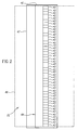
- FIG. 2 shows a bottom view of an illustration of one embodiment of a conventional thermal printhead 22 with an array of thermal resistors 43 fabricated in a ceramic substrate 45.
- a heat sink 47 typically in the form of an aluminum backing plate, is fixed to a left side 49 of ceramic substrate 45. Heat sink 47 rapidly dissipates heat generated by the thermal resistors 43 during printing.
- thermal resistors 43 are arranged in a linear array extending across platen roller 46 (shown in phantom). Such a linear arrangement of thermal resistors 43 is commonly known as a heat line or print line. However, other non-linear arrangements of thermal resistors 43 can be used. Further, it will be appreciated that there are a wide variety of other arrangements of thermal resistors 43 and thermal printheads 22 that can be used in conjunction with the present invention.
- Thermal resistors 43 are adapted to generate heat in proportion to an amount of electrical energy that passes through thermal resistors 43.
- controller 20 transmits signals to a circuit board 51 to which thermal resistors 43 are connected causing different amounts of electrical energy to be applied to thermal resistors 43 so as to selectively heat donor web 30 in a manner that is intended to cause donor material from donor patches 34, 36, 38, and 40 to be applied to receiver web 26 in a desirable manner.
- donor web 30 comprises a first donor patch set 32.1 having a yellow donor patch 34.1, a magenta donor patch 36.1, a cyan donor patch 38.1, a clear donor patch 40.1; and a second donor patch set 32.2 having a yellow donor patch 34.2, a magenta donor patch 36.2, a cyan donor patch 38.2, and a clear donor patch 40.2.
- Each donor patch set 32 has a leading edge L and a trailing edge T.
- the four patches of each set 32.1 and 32.2; etc. are printed, in registration with each other, onto a common image receiving area 52 of receiver web 26 shown in FIG. 4 .
- Circuit board 51 provides variable electrical signals to thermal resistors 43 in accordance with the signal from controller 20.
- a first color is printed in the conventional direction, from right to left as seen by the viewer in FIGS. 1 and 3 .
- controller 20 raises thermal printhead 22 and actuates donor web supply roller 50 and donor web take-up roller 48 to advance a leading edge L of a first donor patch set 32.1 to thermal printhead 22.
- leading edge L for first donor patch set 32.1 is defined by a leading edge of a yellow donor patch 34.1.
- the position of this leading edge L can be determined by using a position sensor to detect a marking indicia on donor web 30 that has a known position relative to the leading edge of yellow donor patch 34.1 or by directly detecting leading edge of yellow donor patch 34.1 as will be discussed in greater detail below.
- Controller 20 also actuates receiver web take-up roller 42 and receiver web supply roller 44 so that image receiving area 52 of receiver web 26 is positioned with respect to the thermal printhead 22.
- image receiving area 52 is defined by a leading edge LER and a trailing edge TER on receiver web 26.
- Donor web 30 and receiver web 26 are positioned so that leading edge LED of yellow donor patch 34.1 is registered at thermal printhead 22 with leading edge LER of image receiving area 52.
- Controller 20 then causes a motor or other conventional structure (not shown) to lower thermal printhead 22 so that a lower surface of donor web 30 engages receiver web 26 which is supported by platen roller 46. This creates a pressure holding donor web 30 against receiver web 26.
- Controller 20 then actuates receiver web take-up roller 42, receiver web supply roller 44, donor web take-up roller 48, and donor web supply roller 50 to move receiver web 26 and donor web 30 together past the thermal printhead 22. Concurrently, controller 20 selectively operates heater elements in thermal printhead 22 to transfer donor material yellow donor patch 34.1 to receiver web 26.
- a stripping plate 54 separates donor web 30 from receiver web 26.
- Donor web 30 continues over idler roller 56 toward the donor web take-up roller 48.
- the trailing edge TER of image receiving area 52 of receiver web 26 remains on platen roller 46.
- Controller 20 then adjusts the position of donor web 30 and receiver web 26 using a predefined pattern of donor web movement so that a leading edge of each of the remaining donor patches 36.1, 38.1 and 40.1 in the first donor patch set 32.1 are brought into alignment with leading edge LER of image receiving area 52 and the printing process is repeated to transfer further material as desired to complete image format.
- Controller 20 operates the printer 18 based upon input signals from a user input system 62, an output system 64, a memory 68, a communication system 74, and sensor system 80.
- User input system 62 can comprise any form of transducer or other device capable of receiving an input from a user and converting this input into a form that can be used by controller 20.
- user input system 62 can comprise a touch screen input, a touch pad input, a 4-way switch, a 6-way switch, an 8-way switch, a stylus system, a trackball system, a joystick system, a voice recognition system, a gesture recognition system or other such systems.
- An output system 64 such as a display, is optionally provided and can be used by controller 20 to provide human perceptible signals for feedback, informational or other purposes.
- Memory 68 can take many forms and can include without limitation conventional memory devices including solid state, magnetic, optical or other data storage devices.
- memory 68 is shown having a removable memory interface 71 for communicating with removable memory (not shown) such as a magnetic, optical or magnetic disks.
- memory 68 is also shown having a hard drive 72 that is fixed with printer 18 and a remote memory 76 that is external to controller 20 such as a personal computer, computer network or other imaging system.
- controller 20 has a communication system 74 for communicating external devices such as remote memory 76.
- Communication system 74 can be for example, an optical, radio frequency circuit or other transducer that converts electronic signals representing an image and other data into a form that can be conveyed to a separate device by way of an optical signal, radio frequency signal or other form of signal.
- Communication system 74 can also be used to receive a digital image and other information from a host computer or network (not shown). Controller 20 can also receive information and instructions from signals received by communication system 74.
- Sensor system 80 includes circuits and systems that are adapted to detect conditions within printer 18 and, optionally, in the environment surrounding printer 18 and to convert this information into a form that can be used by controller 20 in governing printing operations. Sensor system 80 can take a wide variety of forms depending on the type of media therein and the operating environment in which printer 18 is to be used.
- sensor system 80 includes an optional donor position sensor 82 that is adapted to detect the position of donor web 30 and a receiver web position sensor 84. Controller 20 cooperates with donor position sensor 82 to monitor donor web 30 during movement thereof so that controller 20 can detect one or more conditions on donor web 30 that indicate a leading edge of a donor patch set.
- a donor web 30 can be provided that has markings or other optically, magnetically or electronically sensible indicia between each donor patch set 32 and/or between donor patches 34, 36, 38, and 40. Where such markings or indicia are provided, donor position sensor 82 is provided to sense these markings or indicia and to provide signals to controller 20.
- Controller 20 can use these markings and indicia to determine when donor web 30 is positioned with the leading edge of the donor patch set at thermal printhead 22. In a similar way, controller 20 can use signals from receiver web position sensor 84 to monitor the position of the receiver web 26 to align receiver web 26 during printing. Receiver web position sensor 84 can be adapted to sense markings or other optically, magnetically or electronically sensible indicia between each image receiving area of receiver web 26.
- controller 20 causes donor web 30 to be advanced in a predetermined pattern of distances so as to cause a leading edge of each of the first donor patches 34.1, 36.1, 38.1, and 40.1 to be properly positioned relative to the image receiving area 52 at the start each printing process.
- Controller 20 can optionally be adapted to achieve such positioning by precise control of the movement of donor web 30 using a stepper type motor for motorizing donor web take-up roller 48 or donor web supply roller 50 or by using a movement sensor 86 that can detect movement of donor web 30.
- an arrangement using a receiver web position sensor 84, a follower wheel 88 is provided that engages donor web 30 and moves therewith.
- Follower wheel 88 can have surface features that are optically, magnetically or electronically sensed by movement sensor 86.
- a follower wheel 88 that has markings thereon indicative of an extent of movement of donor web 30 and a movement sensor 86 that has a light sensor that can sense light reflected by the markings.
- perforations, cutouts or other routine and detectable indicia can be incorporated onto donor web 30 in a manner that enables movement sensor 84 to provide an indication of the extent of movement of the donor web 30.
- donor position sensor 82 can also optionally be adapted to sense the color of donor patches on donor web 30 and can provide color signals to controller 20.
- controller 20 is programmed or otherwise adapted to detect a color that is known to be found in the first donor patch, e.g., yellow donor patch 34.1 in a donor patch set such as first donor patch set 32.1. When the first color is detected, controller 20 can determine that donor web 30 is positioned proximate to the start of a donor patch set.
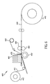
- An exemplary thermal printer schematic 400 shown in FIG. 6 , includes a donor supply spool 410 for distributing a donor web 415.
- a donor take-up spool 420 removes slack donor web 415.
- a receiver supply spool 440 distributes receiver web 445.
- Receiver web 445 and donor web 415 are merged together atop platen roller 450 and beneath a thermal ceramic printhead 460 that includes a grounded heat sink and a peel member 470.
- the peel member 470 separates the donor web 415 from the receiver web 445.
- Donor web 415 continues to travel on to the donor take-up spool 420, while the receiver web 445 travels between a pinch roller 480 and a micro-grip roller 485 that form a nip.
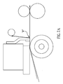
- peel member 470 is metal and ungrounded, i.e., not electrically connected to the earth, yet thermally conductive. Hence, peel member 470 is electrically isolated from ground. The electrical isolation of the peel member 470 from ground removes build-up of electrical charge static charge at a point on the peel member 470 where either one or both of the donor web 415 or the receiver web 445 contact peel member 470 (shown in FIG. 5 ). Therefore, at contact point "A" there will be no apparent electrical static charge transfer as a result of either donor web 415 or receiver web 445 contacting peel member 470.
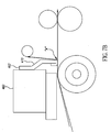
- an alternative embodiment includes a resistance of at least one mega-ohm provided by a high resistance component 462 that substantially electrically isolates peel member 470 from thermal printhead 461 with heat sink 465.
- Peel member 470 can be a plate, a roller, or a bar. Alternatively, peel member 470 can be a combination of either - a plate, roller, or bar. Sources of resistance, that enable electrical isolation of peel member 470 from thermal printhead with heat sink 465 can include non-conductive tape and plastic washers.
- FIG. 8 illustrates a triboelectric effect (increased static charge) when the conductive surface of peel member 470 is grounded to the frame of a thermal printer. Electrostatic charge transfer to the peel member 470 creates an imbalance in electrostatic charge on a donor web or a receiver web that can cause buckling of print media, either a receiver sheet or a donor sheet. Most likely, the receiver sheet is more negatively impacted because the receiver sheet will have difficulty exiting the printer.
- FIG. 9 illustrates that there is minimal or substantially reduced electrostatic charge transferred to peel member 470 when peel member 470 is electrically isolated from ground. Elimination of, or greatly reduced electrostatic charge transfer to the peel member 470 (as shown in FIG. 9 ), ensures substantially reduced migration of charge and keeps near balance of existing charges on both the non-polar surface of receiver web 445 and the non-polar surface of donor web 415.
- a view of a triboelectric effect illustrates that the donor web 415 and the receiver web 445, together at a contact point "A" on peel member 470 generates an electrostatic field.
- a grounded peel member 470 allows a portion of the static charge to go to ground, resulting in a polar charge on the receiver.
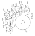
- FIG. 11 A prior-art multi-headed printer is illustrated in FIG. 11 .
- the present invention can be employed for a multi-headed printer as well. In this case, one or more peel plates would be used.
- a print engine 1110 is provided that comprises a receiver transport system and three or more thermal printhead assemblies 1112, 1114 and 1116.
- Each of the printhead assemblies includes a respective re-loadable thermal ribbon cassette assembly which is loaded with a color transfer ribbon 1112c, 1114c, and 1116c.
- Each of the thermal printhead assemblies comprises a thermal printhead 1119a-d having a thermal print line.
- Each of the thermal printhead assemblies further has a counterpart platen roller 1113a-d with which a respective printhead forms a respective nip and through which a receiver 1111 passes in combination with the respective color ribbon of dye.
- the mounting assemblies allow the thermal printheads' positions to be adjusted so that the mounting assemblies can be pivoted towards and away from the respective platen rollers. In this regard, the mounting assemblies are pivotable between an "up" position, wherein the thermal printheads are disengaged from the platen rollers and a "down" position wherein the printheads are in biased engagement with the platen rollers.
- Each reloadable ribbon cassette assembly comprises a cassette body including a ribbon supply roll 1112a, 1114a or 1116a and a ribbon take-up roll 1112b, 1114b or 1116b.
- the ribbon cassette assemblies are loaded with one of three or more primary color ribbons 1112c, 1114c, and 1116c, which are used in conventional subtractive color printing.
- the supply and take-up rolls of each ribbon cassette assembly are coupled to individual ribbon drive sub-assemblies when the cassette assembly is loaded into the printer for printing images on the receiver.
- a ribbon cassette assembly 1118 that is provided with a supply of transparent ribbon 1118c that can transfer an overcoat layer to the receiver after an image has been printed thereon.
- the transparent ribbon cassette assembly is similar in all respects to the other assemblies (including supply and take-up rolls 1118a and 1118b), and a separate printhead is used to transfer the overcoat layer to the now imaged receiver.
- Different types of transparent ribbon may be used to provide matt or glossy finish overcoats to the final print.
- the printhead associated with the transparent ribbon may have the respective recording elements suitably modulated to create different finish overcoats to the final print.
- Receiver 1111 having a coating thereon for receiving a thermal dye is supported as a continuous roll and threaded about platen rollers 1113a-d.
- the receiver is also threaded through a nip comprised of a capstan drive roller 1117 and a back-up roller 1117a.
- a respective color dye image is transferred to the receiver sheet to form the multicolor image.
- thermal printhead assembly 1112 may provide a yellow color separation image
- thermal printhead assembly 1114 may provide a magenta color separation image
- thermal printhead assembly 1116 may provide a cyan color separation image to form a three color multicolor image on the receiver sheet.
- Fourth ribbon cassette assembly 1118 thermally transfers the transparent overcoat to protect the color image from for example fingerprints.
- a thermal printhead 1119a-d that has recording elements selectively enabled in accordance with image information to selectively transfer color dye to the receiver or in the case of the transparent ribbon to transfer the overcoat layer to the now imaged receiver sheet.
- platen rollers 1113a-d form a respective printing nip with the respective printhead 1119a-d.
- the movement of the receiver advances corresponding primary color ribbon 1112c, 1114c, 1116c and 1118c through the respective nip as well.
- a cutter 1115 may be enabled to cut the receiver into a discrete sheet containing the multicolor image protected by the transparent overcoat layer.
- FIG. 12 shows an apparatus for measuring surface voltage including, an isolated metal surface plate 1205 having a plurality of vacuum holes 1210 on its surface.
- a black image sample 1215 on a sheet of receiver material has adhered to its surface dual volt meter probes 1220. These dual volt meter probes 1220 are capable of being positioned in different locations on the black image sample 1215.
- Sample voltage readings from volt meters 1230, 1240 when electrically connected to dual volt meter probes 1220 provide useful data on the amount of voltage difference between a grounded member and an isolated peel plate. Peel members can be plates.
- Probes from two TrekTM Model 347 Electrostatic Voltmeters are placed over an isolated metal plate (see FIG. 12 ) and calibrated to give zero response according to the manufacturer's procedure.
- a sheet of receiver material is placed on the metal plate with the imaged side uppermost.
- the metal plate contains holes connected to a vacuum pump to ensure intimate contact with the sheet of receiver material.
- the probes are moved over the surface of the sheet, maintaining a constant probe-sheet gap by using a supporting bar which slides across the metal plate. Surface voltage is recorded at selected positions along the sheet of receiver material.
Landscapes
- Electronic Switches (AREA)
- Accessory Devices And Overall Control Thereof (AREA)
- Folding Of Thin Sheet-Like Materials, Special Discharging Devices, And Others (AREA)
- Impression-Transfer Materials And Handling Thereof (AREA)
Description
- The present invention relates to thermal printers of type that apply material from a donor web to a receiver web in order to form images on the receiver web.
- In thermal printing, it is generally well known to render images by heating and pressing one or more donor materials such as a dye, colorant or other coating against a receiver web. The donor materials are provided in sized donor patches on a movable web known as a donor ribbon. The donor patches are organized on the ribbon into donor sets; each set containing all of the donor patches that are to be used to record an image on the receiver web. For full color images, multiple color dye patches can be used, such as yellow, magenta, and cyan donor dye patches. Arrangements of other color patches can be used in like fashion within a donor set. Additionally, each donor set can include an overcoat or sealant layer.
- Thermal printers offer a wide range of advantages in photographic printing including the provision of truly continuous tone scale variation and the ability to deposit, as a part of the printing process a protective overcoat layer to protect the images formed thereby from mechanical and environmental damage. Accordingly, the most popular photographic kiosks and home photo printers currently use thermal printing technology.
- Electrostatic charge can be generated in thermal printers by peeling donor media from receiver media. Electrostatic charge is a significant concern and problem for makers of thermal printers, because excess static charge leads to jamming and buckling of print media as the print media traverses through the thermal printer. Conventional approaches to addressing static charge focus on the media itself in that, ionic or nonionic anti-stats are added to the media; for example, the receiver media. This anti-static material is adjusted positionally to reduce static charge. In other words, the anti-static material may be placed in multiple locations with varying effectiveness. The anti-stats may be placed in various layers of the receiver and donor media.
- Limitations of anti-stats include, for ionic anti-stats, their ineffectiveness in high humidity. Both ionic and non-ionic anti-stats are subject to great expense, and imprecise usage that is dependent upon the receiver media impacted with reduction of static charge. Another disadvantage associated with non-ionic anti-stats is an addition of unwanted color in white areas of a print.
-
JP-A-630147168 - One aspect of the present invention thermal printer according to claim 1.
- Another aspect of the invention provides a method for eliminating built-up electrical static charge in a thermally conductive peel member assembly according to claim 3.
-
-
FIG. 1 shows a printer having one embodiment of the control system of the invention; -
FIG. 2 shows a bottom view of one embodiment of a thermal printhead used in the printer ofFIG. 1 ; -
FIG. 3 shows a donor web; -
FIG. 4 shows a thermal printhead, platen, donor web, and receiver web during printing; -
FIG. 5 shows a thermal printhead, platen, donor web, and receiver web during printing; -
FIG. 6 illustrates an exemplary thermal printer system; -
FIG. 7 illustrates electrical isolation from ground of peel member assembly; -
FIG. 8 illustrates a triboelectric effect upon the peel member assembly; -
FIG. 9 illustrates no triboelectric effect upon the peel member assembly; -
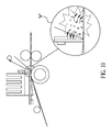
FIG. 10 illustrates triboelectric effect at critical contact point for peel member, donor web, and receiver web; -
FIG. 11 illustrates a prior art multi-headed printer; and -
FIG. 12 shows an apparatus for measuring surface voltage on a sheet of receiver material. -
FIG. 1 shows one exemplary embodiment aprinter 18 of the invention. As shown inFIG. 1 ,printer 18 has acontroller 20 that causesthermal printhead 22 to record images on areceiver web 26 by applying heat and pressure to transfer material from adonor web 30 toreceiver web 26.Controller 20 can include, but is not limited to: a programmable digital computer, a programmable microprocessor, a programmable logic controller, a series of electronic circuits, a series of electronic circuits reduced to the form of an integrated circuit, or a series of discrete components. In the embodiment ofFIG. 1 ,controller 20 also controls a receiver web take-up roller 42, a receiverweb supply roller 44, a donor web take-up roller 48, and a donorweb supply roller 50; which are each motorized for rotation on command of thecontroller 20 to effect movement ofreceiver web 26 anddonor web 30. -
FIG. 2 shows a bottom view of an illustration of one embodiment of a conventionalthermal printhead 22 with an array ofthermal resistors 43 fabricated in aceramic substrate 45. Aheat sink 47, typically in the form of an aluminum backing plate, is fixed to aleft side 49 ofceramic substrate 45.Heat sink 47 rapidly dissipates heat generated by thethermal resistors 43 during printing. In the embodiment shown inFIG. 2 ,thermal resistors 43 are arranged in a linear array extending across platen roller 46 (shown in phantom). Such a linear arrangement ofthermal resistors 43 is commonly known as a heat line or print line. However, other non-linear arrangements ofthermal resistors 43 can be used. Further, it will be appreciated that there are a wide variety of other arrangements ofthermal resistors 43 andthermal printheads 22 that can be used in conjunction with the present invention. -
Thermal resistors 43 are adapted to generate heat in proportion to an amount of electrical energy that passes throughthermal resistors 43. During printing,controller 20 transmits signals to acircuit board 51 to whichthermal resistors 43 are connected causing different amounts of electrical energy to be applied tothermal resistors 43 so as to selectivelyheat donor web 30 in a manner that is intended to cause donor material from donor patches 34, 36, 38, and 40 to be applied toreceiver web 26 in a desirable manner. - As is shown in
FIG. 3 ,donor web 30 comprises a first donor patch set 32.1 having a yellow donor patch 34.1, a magenta donor patch 36.1, a cyan donor patch 38.1, a clear donor patch 40.1; and a second donor patch set 32.2 having a yellow donor patch 34.2, a magenta donor patch 36.2, a cyan donor patch 38.2, and a clear donor patch 40.2. Each donor patch set 32 has a leading edge L and a trailing edge T. In order to provide a full color image with a clear protective coating, the four patches of each set 32.1 and 32.2; etc., are printed, in registration with each other, onto a commonimage receiving area 52 ofreceiver web 26 shown inFIG. 4 .Circuit board 51 provides variable electrical signals tothermal resistors 43 in accordance with the signal fromcontroller 20. - A first color is printed in the conventional direction, from right to left as seen by the viewer in
FIGS. 1 and3 . During printing,controller 20 raisesthermal printhead 22 and actuates donorweb supply roller 50 and donor web take-up roller 48 to advance a leading edge L of a first donor patch set 32.1 tothermal printhead 22. In the embodiment illustrated inFIGS. 1 through 3 , leading edge L for first donor patch set 32.1 is defined by a leading edge of a yellow donor patch 34.1. As will be discussed in greater detail below, the position of this leading edge L can be determined by using a position sensor to detect a marking indicia ondonor web 30 that has a known position relative to the leading edge of yellow donor patch 34.1 or by directly detecting leading edge of yellow donor patch 34.1 as will be discussed in greater detail below. -
Controller 20 also actuates receiver web take-up roller 42 and receiverweb supply roller 44 so thatimage receiving area 52 ofreceiver web 26 is positioned with respect to thethermal printhead 22. In the embodiment illustrated,image receiving area 52 is defined by a leading edge LER and a trailing edge TER onreceiver web 26. Donorweb 30 andreceiver web 26 are positioned so that leading edge LED of yellow donor patch 34.1 is registered atthermal printhead 22 with leading edge LER ofimage receiving area 52.Controller 20 then causes a motor or other conventional structure (not shown) to lowerthermal printhead 22 so that a lower surface ofdonor web 30 engagesreceiver web 26 which is supported byplaten roller 46. This creates a pressure holdingdonor web 30 againstreceiver web 26. -
Controller 20 then actuates receiver web take-up roller 42, receiverweb supply roller 44, donor web take-up roller 48, and donorweb supply roller 50 to movereceiver web 26 anddonor web 30 together past thethermal printhead 22. Concurrently,controller 20 selectively operates heater elements inthermal printhead 22 to transfer donor material yellow donor patch 34.1 toreceiver web 26. - As
donor web 30 andreceiver web 26 leave thethermal printhead 22, a strippingplate 54 separatesdonor web 30 fromreceiver web 26.Donor web 30 continues over idler roller 56 toward the donor web take-uproller 48. As shown inFIG. 4 , the trailing edge TER ofimage receiving area 52 ofreceiver web 26 remains onplaten roller 46.Controller 20 then adjusts the position ofdonor web 30 andreceiver web 26 using a predefined pattern of donor web movement so that a leading edge of each of the remaining donor patches 36.1, 38.1 and 40.1 in the first donor patch set 32.1 are brought into alignment with leading edge LER ofimage receiving area 52 and the printing process is repeated to transfer further material as desired to complete image format. -
Controller 20 operates theprinter 18 based upon input signals from a user input system 62, anoutput system 64, amemory 68, acommunication system 74, andsensor system 80. User input system 62 can comprise any form of transducer or other device capable of receiving an input from a user and converting this input into a form that can be used bycontroller 20. For example, user input system 62 can comprise a touch screen input, a touch pad input, a 4-way switch, a 6-way switch, an 8-way switch, a stylus system, a trackball system, a joystick system, a voice recognition system, a gesture recognition system or other such systems. Anoutput system 64, such as a display, is optionally provided and can be used bycontroller 20 to provide human perceptible signals for feedback, informational or other purposes. - Data including, but not limited to, control programs, digital images and metadata can also be stored in
memory 68.Memory 68 can take many forms and can include without limitation conventional memory devices including solid state, magnetic, optical or other data storage devices. In the embodiment ofFIG. 1 ,memory 68 is shown having aremovable memory interface 71 for communicating with removable memory (not shown) such as a magnetic, optical or magnetic disks. In the embodiment ofFIG. 1 ,memory 68 is also shown having ahard drive 72 that is fixed withprinter 18 and aremote memory 76 that is external tocontroller 20 such as a personal computer, computer network or other imaging system. - In the embodiment shown in
FIG. 1 ,controller 20 has acommunication system 74 for communicating external devices such asremote memory 76.Communication system 74 can be for example, an optical, radio frequency circuit or other transducer that converts electronic signals representing an image and other data into a form that can be conveyed to a separate device by way of an optical signal, radio frequency signal or other form of signal.Communication system 74 can also be used to receive a digital image and other information from a host computer or network (not shown).Controller 20 can also receive information and instructions from signals received bycommunication system 74. -
Sensor system 80 includes circuits and systems that are adapted to detect conditions withinprinter 18 and, optionally, in theenvironment surrounding printer 18 and to convert this information into a form that can be used bycontroller 20 in governing printing operations.Sensor system 80 can take a wide variety of forms depending on the type of media therein and the operating environment in whichprinter 18 is to be used. - In the embodiment of
FIG. 1 ,sensor system 80 includes an optionaldonor position sensor 82 that is adapted to detect the position ofdonor web 30 and a receiverweb position sensor 84.Controller 20 cooperates withdonor position sensor 82 to monitordonor web 30 during movement thereof so thatcontroller 20 can detect one or more conditions ondonor web 30 that indicate a leading edge of a donor patch set. In this regard, adonor web 30 can be provided that has markings or other optically, magnetically or electronically sensible indicia between each donor patch set 32 and/or between donor patches 34, 36, 38, and 40. Where such markings or indicia are provided,donor position sensor 82 is provided to sense these markings or indicia and to provide signals tocontroller 20.Controller 20 can use these markings and indicia to determine whendonor web 30 is positioned with the leading edge of the donor patch set atthermal printhead 22. In a similar way,controller 20 can use signals from receiverweb position sensor 84 to monitor the position of thereceiver web 26 to alignreceiver web 26 during printing. Receiverweb position sensor 84 can be adapted to sense markings or other optically, magnetically or electronically sensible indicia between each image receiving area ofreceiver web 26. - During a full image printing operation,
controller 20 causesdonor web 30 to be advanced in a predetermined pattern of distances so as to cause a leading edge of each of the first donor patches 34.1, 36.1, 38.1, and 40.1 to be properly positioned relative to theimage receiving area 52 at the start each printing process.Controller 20 can optionally be adapted to achieve such positioning by precise control of the movement ofdonor web 30 using a stepper type motor for motorizing donor web take-uproller 48 or donorweb supply roller 50 or by using amovement sensor 86 that can detect movement ofdonor web 30. In one example, an arrangement using a receiverweb position sensor 84, afollower wheel 88 is provided that engagesdonor web 30 and moves therewith.Follower wheel 88 can have surface features that are optically, magnetically or electronically sensed bymovement sensor 86. One example of this is afollower wheel 88 that has markings thereon indicative of an extent of movement ofdonor web 30 and amovement sensor 86 that has a light sensor that can sense light reflected by the markings. In other optional embodiments, perforations, cutouts or other routine and detectable indicia can be incorporated ontodonor web 30 in a manner that enablesmovement sensor 84 to provide an indication of the extent of movement of thedonor web 30. - Alternatively,
donor position sensor 82 can also optionally be adapted to sense the color of donor patches ondonor web 30 and can provide color signals tocontroller 20. In this alternative,controller 20 is programmed or otherwise adapted to detect a color that is known to be found in the first donor patch, e.g., yellow donor patch 34.1 in a donor patch set such as first donor patch set 32.1. When the first color is detected,controller 20 can determine thatdonor web 30 is positioned proximate to the start of a donor patch set. - An exemplary
thermal printer schematic 400, shown inFIG. 6 , includes adonor supply spool 410 for distributing adonor web 415. A donor take-upspool 420 removesslack donor web 415. Areceiver supply spool 440 distributesreceiver web 445.Receiver web 445 anddonor web 415 are merged together atopplaten roller 450 and beneath a thermalceramic printhead 460 that includes a grounded heat sink and apeel member 470. Subsequent to the thermalceramic printhead 460 adhering donor material on thedonor web 415 toreceiver web 445, thepeel member 470 separates thedonor web 415 from thereceiver web 445.Donor web 415 continues to travel on to the donor take-upspool 420, while thereceiver web 445 travels between a pinch roller 480 and amicro-grip roller 485 that form a nip. - In
FIG. 7A ,peel member 470 is metal and ungrounded, i.e., not electrically connected to the earth, yet thermally conductive. Hence,peel member 470 is electrically isolated from ground. The electrical isolation of thepeel member 470 from ground removes build-up of electrical charge static charge at a point on thepeel member 470 where either one or both of thedonor web 415 or thereceiver web 445 contact peel member 470 (shown inFIG. 5 ). Therefore, at contact point "A" there will be no apparent electrical static charge transfer as a result of eitherdonor web 415 orreceiver web 445 contactingpeel member 470. - In
FIG. 7B , an alternative embodiment includes a resistance of at least one mega-ohm provided by ahigh resistance component 462 that substantially electrically isolatespeel member 470 from thermal printhead 461 with heat sink 465. -
Peel member 470 can be a plate, a roller, or a bar. Alternatively,peel member 470 can be a combination of either - a plate, roller, or bar. Sources of resistance, that enable electrical isolation ofpeel member 470 from thermal printhead with heat sink 465 can include non-conductive tape and plastic washers. - Conventional wisdom, involving electrical current and electrical conductive material, states that the electrical conductive material should be grounded. Applicants' novel approach reduces transfer of electrostatic charge, because
peel member 470 is at least substantially electrically isolated.FIG. 8 illustrates a triboelectric effect (increased static charge) when the conductive surface ofpeel member 470 is grounded to the frame of a thermal printer. Electrostatic charge transfer to thepeel member 470 creates an imbalance in electrostatic charge on a donor web or a receiver web that can cause buckling of print media, either a receiver sheet or a donor sheet. Most likely, the receiver sheet is more negatively impacted because the receiver sheet will have difficulty exiting the printer. - In sharp contrast to
FIG.8 ,FIG. 9 illustrates that there is minimal or substantially reduced electrostatic charge transferred to peelmember 470 whenpeel member 470 is electrically isolated from ground. Elimination of, or greatly reduced electrostatic charge transfer to the peel member 470 (as shown inFIG. 9 ), ensures substantially reduced migration of charge and keeps near balance of existing charges on both the non-polar surface ofreceiver web 445 and the non-polar surface ofdonor web 415. - A view of a triboelectric effect, as shown in
FIG. 10 , illustrates that thedonor web 415 and thereceiver web 445, together at a contact point "A" onpeel member 470 generates an electrostatic field. A groundedpeel member 470 allows a portion of the static charge to go to ground, resulting in a polar charge on the receiver. - A prior-art multi-headed printer is illustrated in
FIG. 11 . The present invention can be employed for a multi-headed printer as well. In this case, one or more peel plates would be used. - Referring to
FIG. 11 , reference is to a single pass, multi-color thermal printer of the type described inU.S. Patent No. 5,440,328 . In such a printer, aprint engine 1110 is provided that comprises a receiver transport system and three or morethermal printhead assemblies color transfer ribbon thermal printhead 1119a-d having a thermal print line. Each of the thermal printhead assemblies further has acounterpart platen roller 1113a-d with which a respective printhead forms a respective nip and through which areceiver 1111 passes in combination with the respective color ribbon of dye. The mounting assemblies allow the thermal printheads' positions to be adjusted so that the mounting assemblies can be pivoted towards and away from the respective platen rollers. In this regard, the mounting assemblies are pivotable between an "up" position, wherein the thermal printheads are disengaged from the platen rollers and a "down" position wherein the printheads are in biased engagement with the platen rollers. - Each reloadable ribbon cassette assembly comprises a cassette body including a
ribbon supply roll up roll primary color ribbons ribbon cassette assembly 1118 that is provided with a supply oftransparent ribbon 1118c that can transfer an overcoat layer to the receiver after an image has been printed thereon. The transparent ribbon cassette assembly is similar in all respects to the other assemblies (including supply and take-uprolls -
Receiver 1111 having a coating thereon for receiving a thermal dye is supported as a continuous roll and threaded aboutplaten rollers 1113a-d. The receiver is also threaded through a nip comprised of acapstan drive roller 1117 and a back-uproller 1117a. As the receiver is driven by the capstan drive roller the receiver passes by eachthermal printhead assembly thermal printhead assembly 1112 may provide a yellow color separation image,thermal printhead assembly 1114 may provide a magenta color separation image, andthermal printhead assembly 1116 may provide a cyan color separation image to form a three color multicolor image on the receiver sheet. Fourthribbon cassette assembly 1118 thermally transfers the transparent overcoat to protect the color image from for example fingerprints. At each of the four assemblies there is provided athermal printhead 1119a-d that has recording elements selectively enabled in accordance with image information to selectively transfer color dye to the receiver or in the case of the transparent ribbon to transfer the overcoat layer to the now imaged receiver sheet. At each thermal print assembly,platen rollers 1113a-d, form a respective printing nip with therespective printhead 1119a-d. As the receiver is driven through each of the respective nips, the movement of the receiver advances correspondingprimary color ribbon cutter 1115 may be enabled to cut the receiver into a discrete sheet containing the multicolor image protected by the transparent overcoat layer. -
FIG. 12 shows an apparatus for measuring surface voltage including, an isolatedmetal surface plate 1205 having a plurality ofvacuum holes 1210 on its surface. Ablack image sample 1215 on a sheet of receiver material has adhered to its surface dual volt meter probes 1220. These dualvolt meter probes 1220 are capable of being positioned in different locations on theblack image sample 1215. Sample voltage readings fromvolt meters volt meter probes 1220 provide useful data on the amount of voltage difference between a grounded member and an isolated peel plate. Peel members can be plates. - In addition, the following test procedure for measuring voltages on image side of a printed sheet of receiver material is included below:
- A Kodak Ektatherm™ donor and receiver from media kit type 838-0370 was used in this test. Black imaged samples of receiver material are generated by an experimental printer which transfers yellow, magenta, and cyan dye patches and a protective laminate patch onto the surface of the receiver. Samples were produced with and without grounding of the
printer peel member 1205, and were measured for surface voltage using the procedure described below. - Probes from two Trek™ Model 347 Electrostatic Voltmeters are placed over an isolated metal plate (see
FIG. 12 ) and calibrated to give zero response according to the manufacturer's procedure. A sheet of receiver material is placed on the metal plate with the imaged side uppermost. The metal plate contains holes connected to a vacuum pump to ensure intimate contact with the sheet of receiver material. The probes are moved over the surface of the sheet, maintaining a constant probe-sheet gap by using a supporting bar which slides across the metal plate. Surface voltage is recorded at selected positions along the sheet of receiver material. - Readings from the two Trek™ Model 347 Electrostatic Voltmeters when the sheets of receiver material are mounted to the isolated metal surface plate:
Image Side of Sheet of Receiver Material Voltage Reading Point Grounded Peel Plate Test (Voltage) Isolated Peel Plate Test (Voltage) 1 0 0 2 -210 15 3 -230 15 4 -230 15 5 -225 15 6 -220 15 7 -220 15 8 -175 15 9 -75 0 10 0 0 -
- 18
- Printer
- 20
- Controller
- 22
- Thermal Printhead
- 26
- Receiver Web
- 30
- Donor Web
- 32
- Donor Patch Set
- 32.1
- First Donor Patch
- 32.2
- Second Donor Patch
- 34
- Donor Patch
- 34.1
- Yellow Donor Patch
- 34.2
- Yellow Donor Patch
- 36
- Donor Patch
- 36.1
- Magenta Donor Patch
- 36.2
- Magenta Donor Patch
- 38
- Donor Patch
- 38.1
- Cyan Donor Patch
- 38.2
- Cyan Donor Patch
- 40
- Donor Patches
- 40.1
- Clear Donor Patch
- 40.2
- Clear Donor Patch
- 42
- Receiver Web Take-Up Roller
- 43
- Thermal Resistors
- 44
- Receiver Web Supply Roller
- 45
- Ceramic Substrate
- 46
- Platen Roller
- 47
- Heat Sink
- 48
- Donor Web Take-Up Roller
- 49
- Aluminum Backing Plate
- 50
- Donor Web Supply Roller
- 51
- Circuit Board
- 52
- Image Receiving Area
- 56
- Idler Roller
- 62
- Input System
- 64
- Output System
- 68
- Memory
- 71
- Removable Memory Interface
- 72
- Hard Drive
- 74
- Communication System
- 76
- Remote Memory
- 80
- Sensor System
- 82
- Donor Position Sensor
- 84
- Receiver Web Position Sensor
- 86
- Movement Sensor
- 88
- Follower Wheel
- 400
- Thermal Printer Schematic
- 410
- Donor Supply Spool
- 415
- Donor Web
- 420
- Donor Take-Up Spool
- 440
- Receiver Supply Spool
- 445
- Receiver Web
- 450
- Platen Roller
- 460
- Thermal Ceramic Printhead
- 461
- Thermal Printhead
- 462
- High Resistance Component
- 465
- Heat Sink
- 470
- Peel Member
- 480
- Pinch Roller
- 485
- Micro-Grip Roller
- 1110
- Print Engine
- 1111
- Receiver
- 1112
- Thermal Printhead Assembly
- 1112a
- Ribbon Supply Roll
- 1112b
- Ribbon Take-Up Roll
- 1112c
- Primary Color Ribbon
- 1113a-d
- Platen Roller
- 1114
- Thermal Printhead Assembly
- 1114a
- Ribbon Supply Roll
- 1114b
- Ribbon Take-Up Roll
- 1114c
- Primary Color Ribbon
- 1115
- Cutter
- 1116
- Thermal Printhead Assembly
- 1116a
- Ribbon Supply Roll
- 1116b
- Ribbon Take-Up Roll
- 1116c
- Primary Color Ribbon
- 1117
- Capstan Drive Roller
- 1117a
- Back-Up Roller
- 1118
- Ribbon Cassette Assembly
- 1118c
- Transparent Ribbon
- 1119a-d
- Thermal Printhead
- 1205
- Metal Surface Plate
- 1210
- Vacuum Holes
- 1215
- Black Image Sample
- 1220
- Dual Volt Meter Probes
- 1230
- Volt Meters
- 1240
- Volt Meters
- A
- Contact Point
- L
- Leading Edge
- T
- Trailing Edge
- LED
- Leading Edge
- TED
- Trailing Edge
- LER
- Leading Edge
- TER
- Trailing Edge
Claims (13)
- A thermal printer having reduced electrical charge built at point of separation of a donor web (415) and a receiver web (445), comprising:a) at least one thermal printhead (460; 461);b) at least one platen roller (450) with a nip formed between the at least one thermal printhead and the at least one platen roller through which the donor web and the receiver web can be drawn;c) a heat sink attached to the at least one thermal printhead; andd) a peel member (470) located downstream of the nip; characterised in that it also comprisese) an electrical connection from the peel member (470) to ground, the electrical connection including a high resistance component (462).
- The thermal printer as recited in claim 1, further comprising a support structure for the peel member.
- The thermal printer as recited in claim 1, wherein the peel member (470) is electrically isolated from ground.
- The thermal printer as recited in claim 1, wherein the support structure for the peel member (470) is the heat sink attached to the at least one thermal printhead.
- The thermal printer as recited in claim 1 wherein the peel member (470) is electrically isolated apart from the heat sink when the heat sink itself is electrically connected to ground.
- The thermal printer as recited in claim 1, wherein the high resistance component (462) is a resistor of at least 500 kilo-ohms.
- The thermal printer as recited in claim 1, wherein the high resistance component (462) is an air gap.
- The thermal printer as recited in claim 1, wherein the peel member (470) is a plate.
- The thermal printer as recited in claim 1, wherein the peel member (470) is a non-rotating shaft, commonly referred to in web conveyance as a "shoe".
- The thermal printer as recited in claim 1, wherein the peel member (470) is a roller assembly.
- The thermal printer as recited in claim 1, wherein the peel member (470) is supported within a printer housing.
- The thermal printer as recited in claim 5, wherein the peel member (470) is supported from the heat sink and is separated from direct contact with the heat sink with a dielectric material.
- A method for eliminating built-up electrical static charge in a thermally conductive peel member assembly, comprising the steps of:a) electrically isolating the thermal conductive peel member (470) from ground; andb) maintaining the thermal conductive peel member's physical proximate contact with a heat sink assembly of a thermal printhead.
Applications Claiming Priority (2)
| Application Number | Priority Date | Filing Date | Title |
|---|---|---|---|
| US12/183,529 US8169453B2 (en) | 2008-07-31 | 2008-07-31 | Thermally conductive, electrically isolated peel member assembly |
| PCT/US2009/004198 WO2010014154A1 (en) | 2008-07-31 | 2009-07-20 | Thermally conductive, electrically isolated peel member assembly |
Publications (3)
| Publication Number | Publication Date |
|---|---|
| EP2307201A1 EP2307201A1 (en) | 2011-04-13 |
| EP2307201B1 true EP2307201B1 (en) | 2014-01-08 |
| EP2307201B8 EP2307201B8 (en) | 2014-04-30 |
Family
ID=41203645
Family Applications (1)
| Application Number | Title | Priority Date | Filing Date |
|---|---|---|---|
| EP09788954.7A Not-in-force EP2307201B8 (en) | 2008-07-31 | 2009-07-20 | Thermally conductive, electrically isolated peel member assembly |
Country Status (5)
| Country | Link |
|---|---|
| US (1) | US8169453B2 (en) |
| EP (1) | EP2307201B8 (en) |
| JP (2) | JP2011529413A (en) |
| CN (1) | CN102105308B (en) |
| WO (1) | WO2010014154A1 (en) |
Families Citing this family (4)
| Publication number | Priority date | Publication date | Assignee | Title |
|---|---|---|---|---|
| US8081201B2 (en) * | 2006-08-31 | 2011-12-20 | Dai Nippon Printing Co., Ltd. | Thermal transfer printer |
| CN102744977A (en) * | 2012-07-17 | 2012-10-24 | 山东华菱电子有限公司 | Temperature-sensitive print head |
| JP7152246B2 (en) * | 2018-10-22 | 2022-10-12 | セイコーインスツル株式会社 | Thermal printers and handheld terminals |
| JP7615488B2 (en) * | 2020-12-28 | 2025-01-17 | ブラザー工業株式会社 | Printing device |
Family Cites Families (20)
| Publication number | Priority date | Publication date | Assignee | Title |
|---|---|---|---|---|
| JPS6122649U (en) * | 1984-07-16 | 1986-02-10 | 東芝テック株式会社 | label printer |
| JPS6347168A (en) | 1986-08-18 | 1988-02-27 | Seiko Epson Corp | printing device |
| US4860159A (en) * | 1988-09-12 | 1989-08-22 | The Simco Company, Inc. | Tape dispenser with static neutralizer |
| US5342131A (en) * | 1992-04-24 | 1994-08-30 | Sony Corporation | Tension balancer device for ink ribbon |
| US5440328A (en) * | 1992-10-05 | 1995-08-08 | Atlantek, Inc. | Single-pass multi-color thermal printer |
| JPH07156488A (en) * | 1993-12-07 | 1995-06-20 | Mitsubishi Electric Corp | Color printer and method for manufacturing peeling member thereof |
| JPH08318668A (en) * | 1995-05-25 | 1996-12-03 | Brother Ind Ltd | Thermal transfer printing mechanism and facsimile machine using the same |
| JPH09104153A (en) * | 1995-10-11 | 1997-04-22 | Mitsubishi Electric Corp | Thermal transfer printer |
| JP3101194B2 (en) * | 1995-10-17 | 2000-10-23 | 東芝テック株式会社 | Thermal head and method of manufacturing the same |
| JP3491790B2 (en) * | 1996-01-18 | 2004-01-26 | ブラザー工業株式会社 | Printing device |
| JPH11227308A (en) * | 1998-02-10 | 1999-08-24 | Fuji Photo Film Co Ltd | Image forming apparatus |
| JP2002144616A (en) * | 2000-11-13 | 2002-05-22 | Alps Electric Co Ltd | Thermal transfer line printer |
| US6999108B2 (en) * | 2004-02-17 | 2006-02-14 | Eastman Kodak Company | Method and apparatus for image registration improvements in a printer having plural printing stations |
| JP2005343021A (en) * | 2004-06-03 | 2005-12-15 | Alps Electric Co Ltd | Thermal transfer printer |
| JP2006116783A (en) * | 2004-10-20 | 2006-05-11 | Sony Corp | Thermal transfer print head and image forming apparatus |
| JP2006159653A (en) * | 2004-12-08 | 2006-06-22 | Alps Electric Co Ltd | Thermal printer |
| WO2006090842A1 (en) * | 2005-02-24 | 2006-08-31 | Seiko Epson Corporation | Ribbon cartridge and recording device |
| JP2007001121A (en) | 2005-06-23 | 2007-01-11 | Shinko Electric Co Ltd | Thermal transfer printer |
| US7330201B2 (en) * | 2005-09-28 | 2008-02-12 | Eastman Kodak Company | Thermal printer and method for operating same |
| JP4692748B2 (en) | 2005-10-31 | 2011-06-01 | シンフォニアテクノロジー株式会社 | Thermal transfer printer |
-
2008
- 2008-07-31 US US12/183,529 patent/US8169453B2/en active Active
-
2009
- 2009-07-20 EP EP09788954.7A patent/EP2307201B8/en not_active Not-in-force
- 2009-07-20 JP JP2011521098A patent/JP2011529413A/en active Pending
- 2009-07-20 CN CN200980129560.4A patent/CN102105308B/en not_active Expired - Fee Related
- 2009-07-20 WO PCT/US2009/004198 patent/WO2010014154A1/en not_active Ceased
-
2014
- 2014-11-25 JP JP2014237402A patent/JP2015063138A/en active Pending
Also Published As
| Publication number | Publication date |
|---|---|
| EP2307201B8 (en) | 2014-04-30 |
| JP2015063138A (en) | 2015-04-09 |
| EP2307201A1 (en) | 2011-04-13 |
| CN102105308B (en) | 2013-07-24 |
| CN102105308A (en) | 2011-06-22 |
| WO2010014154A1 (en) | 2010-02-04 |
| JP2011529413A (en) | 2011-12-08 |
| US8169453B2 (en) | 2012-05-01 |
| US20100026776A1 (en) | 2010-02-04 |
Similar Documents
| Publication | Publication Date | Title |
|---|---|---|
| EP3003728B1 (en) | High efficiency printing system for improved image quality | |
| US7330201B2 (en) | Thermal printer and method for operating same | |
| US8708447B2 (en) | Temperature monitoring system for a media preheater | |
| US8169453B2 (en) | Thermally conductive, electrically isolated peel member assembly | |
| US9446600B2 (en) | High efficiency printing method for improved image quality | |
| EP3033235B1 (en) | System and method for determining receiver type in a thermal printer | |
| US7400337B2 (en) | System and method for efficient donor material use | |
| US7324124B2 (en) | Printer and method for detecting donor material | |
| US8585034B1 (en) | Receiver supply using cut sheet media | |
| US10434791B2 (en) | Used transfer layer detection in a transfer printing device | |
| US7397489B2 (en) | System and method for efficient donor material use | |
| JP4300792B2 (en) | Plastic sheet manufacturing method, manufacturing apparatus thereof, and collating apparatus | |
| US8820915B2 (en) | Method for handling cut sheet media | |
| US20060232656A1 (en) | Thermal printer, print head, printing method and substrate for use therewith | |
| JP4019797B2 (en) | Printer apparatus and printing method | |
| US9434569B2 (en) | Offset print stacking tray with waste area | |
| JPH0834128A (en) | Color recording apparatus | |
| JPS58224781A (en) | Recorder |
Legal Events
| Date | Code | Title | Description |
|---|---|---|---|
| PUAI | Public reference made under article 153(3) epc to a published international application that has entered the european phase |
Free format text: ORIGINAL CODE: 0009012 |
|
| 17P | Request for examination filed |
Effective date: 20110127 |
|
| AK | Designated contracting states |
Kind code of ref document: A1 Designated state(s): AT BE BG CH CY CZ DE DK EE ES FI FR GB GR HR HU IE IS IT LI LT LU LV MC MK MT NL NO PL PT RO SE SI SK SM TR |
|
| AX | Request for extension of the european patent |
Extension state: AL BA RS |
|
| RIN1 | Information on inventor provided before grant (corrected) |
Inventor name: ELLIS, RICHARD, HAROLD Inventor name: MINDLER, ROBERT, FREDRIC Inventor name: HILTON, DAVID, BRUCE |
|
| DAX | Request for extension of the european patent (deleted) | ||
| GRAP | Despatch of communication of intention to grant a patent |
Free format text: ORIGINAL CODE: EPIDOSNIGR1 |
|
| INTG | Intention to grant announced |
Effective date: 20130718 |
|
| GRAS | Grant fee paid |
Free format text: ORIGINAL CODE: EPIDOSNIGR3 |
|
| GRAA | (expected) grant |
Free format text: ORIGINAL CODE: 0009210 |
|
| RAP1 | Party data changed (applicant data changed or rights of an application transferred) |
Owner name: KODAK ALARIS INC. |
|
| AK | Designated contracting states |
Kind code of ref document: B1 Designated state(s): AT BE BG CH CY CZ DE DK EE ES FI FR GB GR HR HU IE IS IT LI LT LU LV MC MK MT NL NO PL PT RO SE SI SK SM TR |
|
| REG | Reference to a national code |
Ref country code: GB Ref legal event code: FG4D |
|
| REG | Reference to a national code |
Ref country code: CH Ref legal event code: EP |
|
| REG | Reference to a national code |
Ref country code: IE Ref legal event code: FG4D |
|
| REG | Reference to a national code |
Ref country code: AT Ref legal event code: REF Ref document number: 648457 Country of ref document: AT Kind code of ref document: T Effective date: 20140215 |
|
| REG | Reference to a national code |
Ref country code: DE Ref legal event code: R096 Ref document number: 602009021368 Country of ref document: DE Effective date: 20140220 |
|
| REG | Reference to a national code |
Ref country code: NL Ref legal event code: T3 |
|
| REG | Reference to a national code |
Ref country code: AT Ref legal event code: MK05 Ref document number: 648457 Country of ref document: AT Kind code of ref document: T Effective date: 20140108 |
|
| REG | Reference to a national code |
Ref country code: LT Ref legal event code: MG4D |
|
| PG25 | Lapsed in a contracting state [announced via postgrant information from national office to epo] |
Ref country code: LT Free format text: LAPSE BECAUSE OF FAILURE TO SUBMIT A TRANSLATION OF THE DESCRIPTION OR TO PAY THE FEE WITHIN THE PRESCRIBED TIME-LIMIT Effective date: 20140108 Ref country code: NO Free format text: LAPSE BECAUSE OF FAILURE TO SUBMIT A TRANSLATION OF THE DESCRIPTION OR TO PAY THE FEE WITHIN THE PRESCRIBED TIME-LIMIT Effective date: 20140408 Ref country code: IS Free format text: LAPSE BECAUSE OF FAILURE TO SUBMIT A TRANSLATION OF THE DESCRIPTION OR TO PAY THE FEE WITHIN THE PRESCRIBED TIME-LIMIT Effective date: 20140508 |
|
| PG25 | Lapsed in a contracting state [announced via postgrant information from national office to epo] |
Ref country code: FI Free format text: LAPSE BECAUSE OF FAILURE TO SUBMIT A TRANSLATION OF THE DESCRIPTION OR TO PAY THE FEE WITHIN THE PRESCRIBED TIME-LIMIT Effective date: 20140108 Ref country code: PT Free format text: LAPSE BECAUSE OF FAILURE TO SUBMIT A TRANSLATION OF THE DESCRIPTION OR TO PAY THE FEE WITHIN THE PRESCRIBED TIME-LIMIT Effective date: 20140508 Ref country code: ES Free format text: LAPSE BECAUSE OF FAILURE TO SUBMIT A TRANSLATION OF THE DESCRIPTION OR TO PAY THE FEE WITHIN THE PRESCRIBED TIME-LIMIT Effective date: 20140108 Ref country code: CY Free format text: LAPSE BECAUSE OF FAILURE TO SUBMIT A TRANSLATION OF THE DESCRIPTION OR TO PAY THE FEE WITHIN THE PRESCRIBED TIME-LIMIT Effective date: 20140108 Ref country code: AT Free format text: LAPSE BECAUSE OF FAILURE TO SUBMIT A TRANSLATION OF THE DESCRIPTION OR TO PAY THE FEE WITHIN THE PRESCRIBED TIME-LIMIT Effective date: 20140108 Ref country code: SE Free format text: LAPSE BECAUSE OF FAILURE TO SUBMIT A TRANSLATION OF THE DESCRIPTION OR TO PAY THE FEE WITHIN THE PRESCRIBED TIME-LIMIT Effective date: 20140108 |
|
| PG25 | Lapsed in a contracting state [announced via postgrant information from national office to epo] |
Ref country code: BE Free format text: LAPSE BECAUSE OF FAILURE TO SUBMIT A TRANSLATION OF THE DESCRIPTION OR TO PAY THE FEE WITHIN THE PRESCRIBED TIME-LIMIT Effective date: 20140108 Ref country code: HR Free format text: LAPSE BECAUSE OF FAILURE TO SUBMIT A TRANSLATION OF THE DESCRIPTION OR TO PAY THE FEE WITHIN THE PRESCRIBED TIME-LIMIT Effective date: 20140108 Ref country code: LV Free format text: LAPSE BECAUSE OF FAILURE TO SUBMIT A TRANSLATION OF THE DESCRIPTION OR TO PAY THE FEE WITHIN THE PRESCRIBED TIME-LIMIT Effective date: 20140108 |
|
| REG | Reference to a national code |
Ref country code: DE Ref legal event code: R097 Ref document number: 602009021368 Country of ref document: DE |
|
| PG25 | Lapsed in a contracting state [announced via postgrant information from national office to epo] |
Ref country code: DK Free format text: LAPSE BECAUSE OF FAILURE TO SUBMIT A TRANSLATION OF THE DESCRIPTION OR TO PAY THE FEE WITHIN THE PRESCRIBED TIME-LIMIT Effective date: 20140108 Ref country code: EE Free format text: LAPSE BECAUSE OF FAILURE TO SUBMIT A TRANSLATION OF THE DESCRIPTION OR TO PAY THE FEE WITHIN THE PRESCRIBED TIME-LIMIT Effective date: 20140108 Ref country code: CZ Free format text: LAPSE BECAUSE OF FAILURE TO SUBMIT A TRANSLATION OF THE DESCRIPTION OR TO PAY THE FEE WITHIN THE PRESCRIBED TIME-LIMIT Effective date: 20140108 Ref country code: RO Free format text: LAPSE BECAUSE OF FAILURE TO SUBMIT A TRANSLATION OF THE DESCRIPTION OR TO PAY THE FEE WITHIN THE PRESCRIBED TIME-LIMIT Effective date: 20140108 |
|
| PLBE | No opposition filed within time limit |
Free format text: ORIGINAL CODE: 0009261 |
|
| STAA | Information on the status of an ep patent application or granted ep patent |
Free format text: STATUS: NO OPPOSITION FILED WITHIN TIME LIMIT |
|
| PG25 | Lapsed in a contracting state [announced via postgrant information from national office to epo] |
Ref country code: PL Free format text: LAPSE BECAUSE OF FAILURE TO SUBMIT A TRANSLATION OF THE DESCRIPTION OR TO PAY THE FEE WITHIN THE PRESCRIBED TIME-LIMIT Effective date: 20140108 Ref country code: SK Free format text: LAPSE BECAUSE OF FAILURE TO SUBMIT A TRANSLATION OF THE DESCRIPTION OR TO PAY THE FEE WITHIN THE PRESCRIBED TIME-LIMIT Effective date: 20140108 |
|
| 26N | No opposition filed |
Effective date: 20141009 |
|
| REG | Reference to a national code |
Ref country code: DE Ref legal event code: R097 Ref document number: 602009021368 Country of ref document: DE Effective date: 20141009 |
|
| PG25 | Lapsed in a contracting state [announced via postgrant information from national office to epo] |
Ref country code: LU Free format text: LAPSE BECAUSE OF FAILURE TO SUBMIT A TRANSLATION OF THE DESCRIPTION OR TO PAY THE FEE WITHIN THE PRESCRIBED TIME-LIMIT Effective date: 20140720 |
|
| REG | Reference to a national code |
Ref country code: CH Ref legal event code: PL |
|
| REG | Reference to a national code |
Ref country code: IE Ref legal event code: MM4A |
|
| REG | Reference to a national code |
Ref country code: FR Ref legal event code: ST Effective date: 20150331 |
|
| PG25 | Lapsed in a contracting state [announced via postgrant information from national office to epo] |
Ref country code: LI Free format text: LAPSE BECAUSE OF NON-PAYMENT OF DUE FEES Effective date: 20140731 Ref country code: CH Free format text: LAPSE BECAUSE OF NON-PAYMENT OF DUE FEES Effective date: 20140731 |
|
| PG25 | Lapsed in a contracting state [announced via postgrant information from national office to epo] |
Ref country code: FR Free format text: LAPSE BECAUSE OF NON-PAYMENT OF DUE FEES Effective date: 20140731 Ref country code: SI Free format text: LAPSE BECAUSE OF FAILURE TO SUBMIT A TRANSLATION OF THE DESCRIPTION OR TO PAY THE FEE WITHIN THE PRESCRIBED TIME-LIMIT Effective date: 20140108 |
|
| PG25 | Lapsed in a contracting state [announced via postgrant information from national office to epo] |
Ref country code: IE Free format text: LAPSE BECAUSE OF NON-PAYMENT OF DUE FEES Effective date: 20140720 |
|
| PG25 | Lapsed in a contracting state [announced via postgrant information from national office to epo] |
Ref country code: SM Free format text: LAPSE BECAUSE OF FAILURE TO SUBMIT A TRANSLATION OF THE DESCRIPTION OR TO PAY THE FEE WITHIN THE PRESCRIBED TIME-LIMIT Effective date: 20140108 Ref country code: MC Free format text: LAPSE BECAUSE OF FAILURE TO SUBMIT A TRANSLATION OF THE DESCRIPTION OR TO PAY THE FEE WITHIN THE PRESCRIBED TIME-LIMIT Effective date: 20140108 |
|
| PG25 | Lapsed in a contracting state [announced via postgrant information from national office to epo] |
Ref country code: BG Free format text: LAPSE BECAUSE OF FAILURE TO SUBMIT A TRANSLATION OF THE DESCRIPTION OR TO PAY THE FEE WITHIN THE PRESCRIBED TIME-LIMIT Effective date: 20140108 Ref country code: GR Free format text: LAPSE BECAUSE OF FAILURE TO SUBMIT A TRANSLATION OF THE DESCRIPTION OR TO PAY THE FEE WITHIN THE PRESCRIBED TIME-LIMIT Effective date: 20140409 Ref country code: IT Free format text: LAPSE BECAUSE OF FAILURE TO SUBMIT A TRANSLATION OF THE DESCRIPTION OR TO PAY THE FEE WITHIN THE PRESCRIBED TIME-LIMIT Effective date: 20140108 Ref country code: MT Free format text: LAPSE BECAUSE OF FAILURE TO SUBMIT A TRANSLATION OF THE DESCRIPTION OR TO PAY THE FEE WITHIN THE PRESCRIBED TIME-LIMIT Effective date: 20140108 |
|
| PG25 | Lapsed in a contracting state [announced via postgrant information from national office to epo] |
Ref country code: TR Free format text: LAPSE BECAUSE OF FAILURE TO SUBMIT A TRANSLATION OF THE DESCRIPTION OR TO PAY THE FEE WITHIN THE PRESCRIBED TIME-LIMIT Effective date: 20140108 Ref country code: HU Free format text: LAPSE BECAUSE OF FAILURE TO SUBMIT A TRANSLATION OF THE DESCRIPTION OR TO PAY THE FEE WITHIN THE PRESCRIBED TIME-LIMIT; INVALID AB INITIO Effective date: 20090720 |
|
| PGFP | Annual fee paid to national office [announced via postgrant information from national office to epo] |
Ref country code: GB Payment date: 20160624 Year of fee payment: 8 |
|
| PGFP | Annual fee paid to national office [announced via postgrant information from national office to epo] |
Ref country code: NL Payment date: 20160708 Year of fee payment: 8 |
|
| PGFP | Annual fee paid to national office [announced via postgrant information from national office to epo] |
Ref country code: DE Payment date: 20160801 Year of fee payment: 8 |
|
| REG | Reference to a national code |
Ref country code: DE Ref legal event code: R119 Ref document number: 602009021368 Country of ref document: DE |
|
| REG | Reference to a national code |
Ref country code: NL Ref legal event code: MM Effective date: 20170801 |
|
| GBPC | Gb: european patent ceased through non-payment of renewal fee |
Effective date: 20170720 |
|
| PG25 | Lapsed in a contracting state [announced via postgrant information from national office to epo] |
Ref country code: DE Free format text: LAPSE BECAUSE OF NON-PAYMENT OF DUE FEES Effective date: 20180201 Ref country code: GB Free format text: LAPSE BECAUSE OF NON-PAYMENT OF DUE FEES Effective date: 20170720 Ref country code: NL Free format text: LAPSE BECAUSE OF NON-PAYMENT OF DUE FEES Effective date: 20170801 |
|
| PG25 | Lapsed in a contracting state [announced via postgrant information from national office to epo] |
Ref country code: MK Free format text: LAPSE BECAUSE OF FAILURE TO SUBMIT A TRANSLATION OF THE DESCRIPTION OR TO PAY THE FEE WITHIN THE PRESCRIBED TIME-LIMIT Effective date: 20140108 |