EP2306795A1 - Electric circuit structure - Google Patents
Electric circuit structure Download PDFInfo
- Publication number
- EP2306795A1 EP2306795A1 EP09797941A EP09797941A EP2306795A1 EP 2306795 A1 EP2306795 A1 EP 2306795A1 EP 09797941 A EP09797941 A EP 09797941A EP 09797941 A EP09797941 A EP 09797941A EP 2306795 A1 EP2306795 A1 EP 2306795A1
- Authority
- EP
- European Patent Office
- Prior art keywords
- flexible substrate
- substrate
- liquid crystal
- electric circuit
- nonwoven fabric
- Prior art date
- Legal status (The legal status is an assumption and is not a legal conclusion. Google has not performed a legal analysis and makes no representation as to the accuracy of the status listed.)
- Granted
Links
- 239000000758 substrate Substances 0.000 claims abstract description 184
- 239000004745 nonwoven fabric Substances 0.000 claims abstract description 44
- 239000002390 adhesive tape Substances 0.000 claims abstract description 33
- 239000000463 material Substances 0.000 claims abstract description 23
- 239000004973 liquid crystal related substance Substances 0.000 claims description 67
- 239000011347 resin Substances 0.000 claims description 42
- 229920005989 resin Polymers 0.000 claims description 42
- 239000003990 capacitor Substances 0.000 claims description 28
- 239000011159 matrix material Substances 0.000 claims description 7
- XUIMIQQOPSSXEZ-UHFFFAOYSA-N Silicon Chemical compound [Si] XUIMIQQOPSSXEZ-UHFFFAOYSA-N 0.000 claims description 6
- 229910052710 silicon Inorganic materials 0.000 claims description 6
- 239000010703 silicon Substances 0.000 claims description 6
- 230000005534 acoustic noise Effects 0.000 description 5
- 238000004806 packaging method and process Methods 0.000 description 5
- 229910000679 solder Inorganic materials 0.000 description 5
- 238000010586 diagram Methods 0.000 description 4
- 238000005286 illumination Methods 0.000 description 4
- RYGMFSIKBFXOCR-UHFFFAOYSA-N Copper Chemical compound [Cu] RYGMFSIKBFXOCR-UHFFFAOYSA-N 0.000 description 3
- 239000000853 adhesive Substances 0.000 description 3
- 230000001070 adhesive effect Effects 0.000 description 3
- 230000000052 comparative effect Effects 0.000 description 3
- 239000011889 copper foil Substances 0.000 description 3
- 238000005516 engineering process Methods 0.000 description 3
- 229910052751 metal Inorganic materials 0.000 description 3
- 239000002184 metal Substances 0.000 description 3
- 238000000034 method Methods 0.000 description 3
- 229920000139 polyethylene terephthalate Polymers 0.000 description 3
- 239000005020 polyethylene terephthalate Substances 0.000 description 3
- 238000005476 soldering Methods 0.000 description 3
- 239000006071 cream Substances 0.000 description 2
- 230000000694 effects Effects 0.000 description 2
- 239000011521 glass Substances 0.000 description 2
- 230000002093 peripheral effect Effects 0.000 description 2
- 239000004417 polycarbonate Substances 0.000 description 2
- 229920000515 polycarbonate Polymers 0.000 description 2
- -1 polypropylene Polymers 0.000 description 2
- 239000004065 semiconductor Substances 0.000 description 2
- 239000000126 substance Substances 0.000 description 2
- 239000004743 Polypropylene Substances 0.000 description 1
- 229910052782 aluminium Inorganic materials 0.000 description 1
- XAGFODPZIPBFFR-UHFFFAOYSA-N aluminium Chemical compound [Al] XAGFODPZIPBFFR-UHFFFAOYSA-N 0.000 description 1
- 238000001816 cooling Methods 0.000 description 1
- 229920001577 copolymer Polymers 0.000 description 1
- 238000009295 crossflow filtration Methods 0.000 description 1
- 238000009792 diffusion process Methods 0.000 description 1
- 230000005684 electric field Effects 0.000 description 1
- 239000004744 fabric Substances 0.000 description 1
- 239000011888 foil Substances 0.000 description 1
- 230000010365 information processing Effects 0.000 description 1
- 238000009413 insulation Methods 0.000 description 1
- 238000002844 melting Methods 0.000 description 1
- 230000008018 melting Effects 0.000 description 1
- 230000003287 optical effect Effects 0.000 description 1
- 239000002245 particle Substances 0.000 description 1
- 239000004033 plastic Substances 0.000 description 1
- 229920003023 plastic Polymers 0.000 description 1
- 229920000728 polyester Polymers 0.000 description 1
- 229920001155 polypropylene Polymers 0.000 description 1
- 238000007639 printing Methods 0.000 description 1
- 230000000644 propagated effect Effects 0.000 description 1
- 239000003566 sealing material Substances 0.000 description 1
- 239000012209 synthetic fiber Substances 0.000 description 1
- 229920002994 synthetic fiber Polymers 0.000 description 1
Images


Classifications
-
- G—PHYSICS
- G02—OPTICS
- G02F—OPTICAL DEVICES OR ARRANGEMENTS FOR THE CONTROL OF LIGHT BY MODIFICATION OF THE OPTICAL PROPERTIES OF THE MEDIA OF THE ELEMENTS INVOLVED THEREIN; NON-LINEAR OPTICS; FREQUENCY-CHANGING OF LIGHT; OPTICAL LOGIC ELEMENTS; OPTICAL ANALOGUE/DIGITAL CONVERTERS
- G02F1/00—Devices or arrangements for the control of the intensity, colour, phase, polarisation or direction of light arriving from an independent light source, e.g. switching, gating or modulating; Non-linear optics
- G02F1/01—Devices or arrangements for the control of the intensity, colour, phase, polarisation or direction of light arriving from an independent light source, e.g. switching, gating or modulating; Non-linear optics for the control of the intensity, phase, polarisation or colour
- G02F1/13—Devices or arrangements for the control of the intensity, colour, phase, polarisation or direction of light arriving from an independent light source, e.g. switching, gating or modulating; Non-linear optics for the control of the intensity, phase, polarisation or colour based on liquid crystals, e.g. single liquid crystal display cells
- G02F1/133—Constructional arrangements; Operation of liquid crystal cells; Circuit arrangements
- G02F1/1333—Constructional arrangements; Manufacturing methods
- G02F1/1345—Conductors connecting electrodes to cell terminals
- G02F1/13452—Conductors connecting driver circuitry and terminals of panels
-
- H—ELECTRICITY
- H04—ELECTRIC COMMUNICATION TECHNIQUE
- H04M—TELEPHONIC COMMUNICATION
- H04M1/00—Substation equipment, e.g. for use by subscribers
- H04M1/02—Constructional features of telephone sets
- H04M1/0202—Portable telephone sets, e.g. cordless phones, mobile phones or bar type handsets
- H04M1/026—Details of the structure or mounting of specific components
- H04M1/0266—Details of the structure or mounting of specific components for a display module assembly
-
- H—ELECTRICITY
- H05—ELECTRIC TECHNIQUES NOT OTHERWISE PROVIDED FOR
- H05K—PRINTED CIRCUITS; CASINGS OR CONSTRUCTIONAL DETAILS OF ELECTRIC APPARATUS; MANUFACTURE OF ASSEMBLAGES OF ELECTRICAL COMPONENTS
- H05K3/00—Apparatus or processes for manufacturing printed circuits
- H05K3/0058—Laminating printed circuit boards onto other substrates, e.g. metallic substrates
- H05K3/0061—Laminating printed circuit boards onto other substrates, e.g. metallic substrates onto a metallic substrate, e.g. a heat sink
-
- H—ELECTRICITY
- H05—ELECTRIC TECHNIQUES NOT OTHERWISE PROVIDED FOR
- H05K—PRINTED CIRCUITS; CASINGS OR CONSTRUCTIONAL DETAILS OF ELECTRIC APPARATUS; MANUFACTURE OF ASSEMBLAGES OF ELECTRICAL COMPONENTS
- H05K1/00—Printed circuits
- H05K1/02—Details
- H05K1/14—Structural association of two or more printed circuits
- H05K1/141—One or more single auxiliary printed circuits mounted on a main printed circuit, e.g. modules, adapters
-
- H—ELECTRICITY
- H05—ELECTRIC TECHNIQUES NOT OTHERWISE PROVIDED FOR
- H05K—PRINTED CIRCUITS; CASINGS OR CONSTRUCTIONAL DETAILS OF ELECTRIC APPARATUS; MANUFACTURE OF ASSEMBLAGES OF ELECTRICAL COMPONENTS
- H05K1/00—Printed circuits
- H05K1/02—Details
- H05K1/14—Structural association of two or more printed circuits
- H05K1/147—Structural association of two or more printed circuits at least one of the printed circuits being bent or folded, e.g. by using a flexible printed circuit
-
- H—ELECTRICITY
- H05—ELECTRIC TECHNIQUES NOT OTHERWISE PROVIDED FOR
- H05K—PRINTED CIRCUITS; CASINGS OR CONSTRUCTIONAL DETAILS OF ELECTRIC APPARATUS; MANUFACTURE OF ASSEMBLAGES OF ELECTRICAL COMPONENTS
- H05K2201/00—Indexing scheme relating to printed circuits covered by H05K1/00
- H05K2201/05—Flexible printed circuits [FPCs]
- H05K2201/056—Folded around rigid support or component
-
- H—ELECTRICITY
- H05—ELECTRIC TECHNIQUES NOT OTHERWISE PROVIDED FOR
- H05K—PRINTED CIRCUITS; CASINGS OR CONSTRUCTIONAL DETAILS OF ELECTRIC APPARATUS; MANUFACTURE OF ASSEMBLAGES OF ELECTRICAL COMPONENTS
- H05K2201/00—Indexing scheme relating to printed circuits covered by H05K1/00
- H05K2201/20—Details of printed circuits not provided for in H05K2201/01 - H05K2201/10
- H05K2201/2018—Presence of a frame in a printed circuit or printed circuit assembly
-
- H—ELECTRICITY
- H05—ELECTRIC TECHNIQUES NOT OTHERWISE PROVIDED FOR
- H05K—PRINTED CIRCUITS; CASINGS OR CONSTRUCTIONAL DETAILS OF ELECTRIC APPARATUS; MANUFACTURE OF ASSEMBLAGES OF ELECTRICAL COMPONENTS
- H05K2201/00—Indexing scheme relating to printed circuits covered by H05K1/00
- H05K2201/20—Details of printed circuits not provided for in H05K2201/01 - H05K2201/10
- H05K2201/2045—Protection against vibrations
-
- H—ELECTRICITY
- H05—ELECTRIC TECHNIQUES NOT OTHERWISE PROVIDED FOR
- H05K—PRINTED CIRCUITS; CASINGS OR CONSTRUCTIONAL DETAILS OF ELECTRIC APPARATUS; MANUFACTURE OF ASSEMBLAGES OF ELECTRICAL COMPONENTS
- H05K2203/00—Indexing scheme relating to apparatus or processes for manufacturing printed circuits covered by H05K3/00
- H05K2203/01—Tools for processing; Objects used during processing
- H05K2203/0191—Using tape or non-metallic foil in a process, e.g. during filling of a hole with conductive paste
Definitions
- the present invention relates to an electric circuit structure, such as a liquid crystal display apparatus, in which a circuit element is mounted on a flexible substrate connected to a circuit board, and particularly relates to an electric circuit structure with which noise due to vibration of the circuit element mounted on the flexible substrate is reduced.
- a panel substrate that constitutes a flat image display device such as a liquid crystal panel serves as a circuit board on the inner surface of which electric circuit elements such as electrodes that function as pixels and metal wiring are formed.
- switching elements such as TFFs are formed and, for example, COG (Chip On Glass) technology that forms part of a driving circuit on the panel is adopted.
- the panel substrate of a liquid crystal panel is provided with electrode terminals for external connection, and various types of signals for image display and a power supply voltage that is necessary for the panel substrate to operate as a circuit board are supplied, for example, from a peripheral circuit board other than the liquid crystal panel by a flexible substrate connected to the electrode terminals.
- the liquid crystal panel, the peripheral circuit board, and furthermore, a backlight and the like are accommodated in a mechanical member, which is called a bezel, in the form of a frame having a closed bottom, and thus, a liquid crystal display apparatus as an electric circuit structure is configured.
- Connecting terminals on one end of the flexible substrate are joined to the electrode terminals of the panel substrate, and the other end of the flexible substrate is folded back to the rear face side of the bezel so as to conform to a side face of the bezel accommodating the liquid crystal panel and is fixed to the rear face of the bezel.
- a circuit element such as a capacitor is mounted on the flexible substrate via a hard resin substrate, if necessary (see Patent Document 1, for example).
- Patent Document 1 JP 2004-020703A
- the circuit element mounted on the flexible substrate may vibrate during operation of the liquid crystal display apparatus and generate noise.
- laminated foil electrodes within the capacitor vibrate when the capacitor is charged and discharged in accordance with the operation of the liquid crystal display apparatus, and this vibration is transmitted from a container of the capacitor to the hard resin substrate on which the capacitor is mounted, and is further conveyed to the mechanical member of the liquid crystal display apparatus, thereby causing a phenomenon called sound generation in which this vibration makes a loud acoustic noise that a user can perceive.
- an electric circuit structure of the present invention includes a mechanical member in the form of a frame having a closed bottom; a circuit board on the surface of which an electric circuit element is formed, the circuit board being accommodated in the mechanical member; a flexible substrate that has a connecting terminal formed on one end of the flexible substrate, the connecting terminal being connected to an electrode terminal formed on the circuit board, and that is folded back and fixed to a rear face of the mechanical member at the other end opposite to the one end; and a circuit element mounted on a portion of the flexible substrate that is folded back to the rear face of the mechanical member, wherein the flexible substrate is fixed to the rear face of the mechanical member via a nonwoven fabric adhesive tape employing a nonwoven fabric as a base material.
- An electric circuit structure includes a mechanical member in the form of a frame having a closed bottom; a circuit board on the surface of which an electric circuit element is formed, the circuit board being accommodated in the mechanical member; a flexible substrate that has a connecting terminal formed on one end of the flexible substrate, the connecting terminal being connected to an electrode terminal formed on the circuit board, and that is folded back and fixed to a rear face of the mechanical member at the other end opposite to the one end; and a circuit element mounted on a portion of the flexible substrate that is folded back to the rear face of the mechanical member, wherein the flexible substrate is fixed to the rear face of the mechanical member via a nonwoven fabric adhesive tape employing a nonwoven fabric as a base material.
- the nonwoven fabric which is the base material for the tape that fixes the flexible substrate to the mechanical member, absorbs and reduces this vibration.
- the vibration of the circuit element mounted on the flexible substrate is transmitted to the mechanical member and becomes significant, and thus is perceived by the user as acoustic noise.
- the circuit element is mounted on a hard resin substrate laminated on the flexible substrate. This allows the circuit element to be reliably mounted.
- the circuit element is a capacitor.
- a silicon resin layer is formed between the nonwoven fabric adhesive tape and the flexible substrate. This allows the flexible substrate and the nonwoven fabric adhesive tape to be fixed to each other with no space between them even in the case where the flexible substrate is curved.
- the electric circuit structure is a liquid crystal display apparatus
- the circuit board is a panel substrate that constitutes a liquid crystal panel in conjunction with an opposing substrate that is fixed to the panel substrate at a predetermined distance therefrom with a liquid crystal layer sandwiched between the substrates.
- the circuit board is an active matrix substrate.
- an electric circuit structure according to the present invention is implemented as a liquid crystal display apparatus that is used as a display of a mobile telephone or a mobile device.
- the electric circuit structure of the present invention is not limited to such a liquid crystal display apparatus and can be widely applied to various types of flat display apparatuses such as an organic or inorganic EL display and a field-emission cold-cathode display apparatus.
- the electric circuit structure of the present invention can be applied not only to the above-described display apparatus module but to various types of circuit modules, such as a driving circuit of an acoustic apparatus or an information processing apparatus, that include a circuit board to whose electrode terminals a flexible substrate on which a circuit element is mounted is connected, the circuit board being accommodated in and integral with a mechanical member.
- the electric circuit structure is used as a liquid crystal display apparatus, the application thereof is not limited to the display for a mobile telephone or a mobile device, and the electric circuit structure also can be used as various types of monitors such as those of personal computers or televisions.
- FIG. 1 is a perspective view of a liquid crystal display apparatus according to the embodiment of the present invention.
- a liquid crystal display apparatus 100 of the present embodiment has a liquid crystal panel 3 constituted by a panel substrate 1 serving as a circuit board and an opposing substrate 2 that is disposed facing the panel substrate with a predetermined distance between each other.
- a pair of polarizing plates 4 is attached to both outer faces of the liquid crystal panel 3, that is, an outside face of the panel substrate 1 and an outside face of the opposing substrate 2.
- the panel substrate 1 is an active matrix substrate, in which pixel electrodes (not shown) arranged in a matrix pattern so as to form a plurality of rows and a plurality of columns are placed on a surface of the panel substrate 1 facing the opposing substrate 2, and the pixel electrodes form a display region 5 of the liquid crystal panel 3 where an image is displayed.
- a plurality of gate lines arranged in the direction of the rows of the pixel electrodes, a plurality of source lines arranged in the direction of the columns of the pixel electrodes, and furthermore, TFTs that are arranged in the vicinity of the points of intersection of the rows and columns intersecting at right angles and that are connected to the respective pixel electrodes are formed in the display region 5 of the panel substrate 1.
- the gate lines, source lines, and TFTs also are omitted from the drawings.
- a sealing material for fixing the panel substrate 1 and the opposing substrate 2 to each other and a liquid crystal layer sandwiched between the panel substrate 1 and the opposing substrate 2 also are omitted from the drawings.
- COG Chip On Glass
- a backlight 8 that emits illumination light that is necessary to display an image on the liquid crystal panel 3 is disposed on a back side of the liquid crystal panel 3.
- the backlight 8 of the liquid crystal display apparatus 100 of the present embodiment is of a type called a sidelight type or edge-light type and is constituted by a flat plate-like light guide and a light source, such as a cold cathode fluorescent tube or a light emitting diode, provided on a side face of the light guide. Illumination light from the light source that has entered the light guide through the side face thereof is repeatedly reflected within the light guide, thus diffused and propagated, and emitted as uniform light from a principal plane of the light guide on the side facing the liquid crystal panel 3.
- the backlight 8 of the liquid crystal display apparatus is not limited to the above-described sidelight type, and it is also possible to use a type called a direct type in which light sources are arranged on the back side of the liquid crystal panel 3 in a planar manner so as to emit light toward the liquid crystal panel 3, and illumination light from the light sources is radiated on the liquid crystal panel via an optical sheet such as a light concentrating sheet or a diffusion sheet.
- the light source is not limited to the cold cathode fluorescent tube or the light emitting diode, and various types of light sources, such as a hot cathode fluorescent tube and an EL light emitter, can be used.
- the liquid crystal panel 3 is not limited to those called a transmissive type or a semi-transmissive type that use illumination light from the backlight 8 to display an image, and the liquid crystal panel 3 of a reflective type in which external light entering through the opposing substrate 2 of the liquid crystal panel 3 is reflected by reflecting electrodes formed on the panel substrate 1 and used to display an image can be employed, in which case the necessity for the backlight 8 itself is eliminated.
- the liquid crystal panel 3 and the backlight 8 are accommodated in a bezel 9, which is a mechanical member in the form of a frame having a closed bottom.
- the bezel 9 is required to be light weight and ensure a certain degree of strength, and is therefore made of a metal such as aluminum or a resin such as plastic.
- a protrusion for holding the liquid crystal panel 3 and the backlight 8 to be accommodated in the bezel may be formed on the inside of a side wall of the bezel 9, and moreover, a protrusion or a depression for fixing the bezel 9 to a frame of an image display portion of a device such as a mobile telephone or a mobile device may be provided on the image display surface side of the liquid crystal panel 3, that is, at an upper end portion in FIG. 1 .
- an opening may be formed in a side wall portion or a bottom portion of the bezel 9 in order to release heat generated from the backlight 8 and various types of circuit components accommodated in the bezel to the outside or in order to reduce the weight of the bezel 9 itself.
- a flexible substrate 10 for applying a signal or a voltage for operating the liquid crystal panel 3 is connected to the electrode terminals 7 formed in the packaging region 6 of the panel substrate 1.
- This flexible substrate 10 is also called an FPC (Flexible Print Circuit) and has a three-layer structure in which micro wiring formed from copper foil or the like is sandwiched between flexible resin films.
- connecting portions (not shown) where the internal copper foil is exposed are formed at positions corresponding to the locations of the electrode terminals 7 formed in the packaging region 6 of the panel substrate 1, and an electrical connection is established by fixing the flexible substrate while aligning the positions of the electrode terminals 7 with the positions of the connecting portions.
- a film material which is called an anisotropic conductive resin (ACF:Anisotropic Conductive Film), containing conductive particles is used.
- ACF anisotropic Conductive Film
- the liquid crystal display apparatus 100 is produced as a module, which is an integrated electric circuit structure, capable of performing image display simply by inputting a predetermined power supply and signal from the outside, and has a control portion 11 in which a semiconductor integrated circuit for performing overall control of the liquid crystal display apparatus 100 is formed.
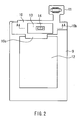
- FIG. 2 is a plan view when the liquid crystal display apparatus 100 of the present embodiment is seen from the rear face, that is, the underside of the image display surface.
- the flexible substrate 10 whose end 10a is connected to the panel substrate 1 on the image display surface side of the liquid crystal display apparatus 100 is folded back to the rear face side along a side face of the bezel 9.
- the flexible substrate 10 has such a shape that part of the bezel 9 is covered with the other end 10b opposite to the end 10a, and is fixed to a rear face of the bezel 9 at this end 10b.
- the flexible substrate 10 is in close contact with the side face of the bezel 9.
- a rear circuit board 12 on which a signal circuit for processing an image signal to be displayed on the liquid crystal panel 3, a driving circuit of the backlight 8 incorporated in the bezel 9, and the like are mounted is disposed on the rear face of the bezel 9, and a protruding portion 10c formed in the end 10b of the flexible substrate 10 is connected to the rear circuit board.
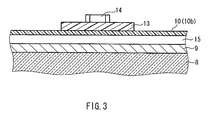
- FIG. 3 is a cross-sectional configuration diagram showing a cross section as seen in the direction of arrow A-A in FIG. 2 and shows an example of the configuration of a portion where the end 10b of the flexible substrate 10 is fixed to the rear face of the bezel 9 and where the capacitor 14 is mounted on the flexible substrate 10 via the resin substrate 13.
- the hard resin substrate 13 is laminated on the flexible substrate 10, and the capacitor 14, which is the circuit element, is mounted on the resin substrate 13.
- a circuit pattern for supporting the mounted capacitor 14 and other circuit elements is formed on the upper face side of the resin substrate 13, and a circuit pattern corresponding to a wiring pattern of the flexible substrate 10 is formed on the lower face side.
- an MCM (multi-chip module) substrate can be used as the resin substrate 13.
- a substrate in which wiring patterns are formed on both faces of a base material such as polycarbonate, which is a common material for a circuit board, a substrate that is a laminate of a plurality pieces of substrates, or the like can be used as the resin substrate 13.
- the capacitor 14 and other circuit elements can be fixed to the resin substrate 13 using ordinary solder.
- the resin substrate 13 and the flexible substrate 10 can be fixed to each other using soldering connection that employs solder bumps or the like with electrode patterns formed on the surfaces of the respective substrates aligned with each other.
- the flexible substrate 10 on which the circuit elements such as the capacitor 14 are mounted via the resin substrate 13 is bonded to the rear face of the bezel 9 via a nonwoven fabric adhesive tape 15 employing a nonwoven fabric (also called an "unwoven fabric") as a base material.
- This nonwoven fabric adhesive tape 15 is a double-sided tape produced by infiltrating a nonwoven fabric made of a synthetic fiber such as polypropylene or polyester and having a thickness of 0.145 mm with an adhesive material.
- FIG. 3 the inside of the bezel 9 is shown up to the backlight 8, and the liquid crystal panel 3 that is disposed below the backlight 8 is omitted.
- the flexible substrate 10 to which the circuit elements such as the capacitor 14 are fixed via the resin substrate 13 is fixed to the rear face of the bezel 9 with the nonwoven fabric adhesive tape 15 employing a soft nonwoven fabric as a base material.
- the nonwoven fabric adhesive tape 15 employing a soft nonwoven fabric as a base material.
- the panel substrate 1 is an active matrix substrate and the liquid crystal panel 3 is driven by active matrix driving
- a control voltage of a driving circuit thereof is applied to the capacitor 14
- a sound generation phenomenon in which vibration of the capacitor 14 causes the bezel 9 to resonate and makes a loud sound, and the user perceives the sound, is likely to occur.
- the liquid crystal display apparatus 100 of the present embodiment the occurrence of this sound generation can be effectively prevented.
- PET polyethylene terephthalate
- a nonwoven fabric-based double-sided adhesive tape "#8800CH(W)" (trade name) having a thickness of 0.145 mm manufactured by Dainippon Ink and Chemicals, Inc.
- a strong-type nonwoven fabric double-sided tape "No. 7566” (product number) having a thickness of 0.160 mm manufactured by Teraoka Seisakusho Co., Ltd., and the like can be used as the nonwoven fabric adhesive tape 15 described in the present embodiment.
- the nonwoven fabric adhesive tape 15 used in the present embodiment which is obtained by impregnating the nonwoven fabric serving as a base material with an adhesive, is a double-sided tape
- the flexible substrate 10 can be extremely easily bonded to the bezel 9.
- the nonwoven fabric adhesive tape 15 is first attached to a region of a bottom face of the bezel 9 to which the flexible substrate 10 is to be fixed, the flexibly substrate 10 is superposed on top of the adhesive tape, and the flexible substrate 10 is pressed down with a pressure of about 300 g to 900 g, whereby a practically sufficient degree of bond strength can be achieved.
- the pressure with which the flexible substrate 10 is pressed down can be determined as appropriate taking the size (area) of the hard resin board 13 fixed to the flexibly substrate 10 or the size, weight, number, arrangement density, or the like of the mounted circuit elements such as the capacitor 14 into consideration.
- FIGS. 4(a) and 4(b) are both cross-sectional configuration diagrams showing the portion where the flexible substrate 10 is fixed to the bezel 9 and show, as in FIG. 3 , the configuration of the portion where the capacitor 14 is mounted on the flexible substrate 10 via the resin substrate 13, that is, the portion as seen in the direction of arrow A-A in FIG. 2 .
- FIGS. 4(a) and 4(b) since the mount state of the capacitor 14 on the flexible substrate 10 and the internal configuration of the bezel 9 are the same as those in FIG. 3 , the components in FIGS. 4(a) and 4(b) are denoted by the same reference numerals as those in FIG. 3 , and detailed descriptions thereof are omitted.
- FIG. 4(a) shows a state in which the flexible substrate 10 is curved along the curvature of the resin substrate 13 fixed to the surface thereof.
- the capacitor 14 and other circuit elements are mounted on the hard resin substrate 13, and soldering is used as a means for securing electrical connection of the circuit elements and fixing the circuit elements.
- soldering is used as a means for securing electrical connection of the circuit elements and fixing the circuit elements.
- a method of printing cream solder onto the surface of the resin substrate 13 then mounting the circuit elements such as the capacitor 14 at predetermined positions, placing the substrate in an infrared reflow oven to melt the cream solder, and thus fixing the circuit components all at once is efficient.
- the portion of the soft flexible substrate 10 that is fixed to the resin substrate 13 deforms so as to conform to the shape of the resin substrate 13. If warping occurs in the flexible substrate 10 in this manner and a gap is created between the flexible substrate and an adhesive tape that fixes the flexible substrate to the bezel 9, vibration of the capacitor 14, which is the mounted circuit element, tends to be transmitted to the bezel 9 as a loud sound.
- the nonwoven fabric adhesive tape 15 itself is soft and can easily adapt to the shape of the flexible substrate 10 even in the case where the flexible substrate is slightly warped as shown in FIG. 4(a) , so that no gap is created.
- the resin substrate 13 is slightly warped, sound generation caused by the vibration of the capacitor 14, which is the circuit element, can be effectively prevented.
- FIG. 4(b) is a cross-sectional configuration diagram showing an example in the case where larger warping than that in FIG. 4(a) has occurred in the resin substrate 13.
- the nonwoven fabric adhesive tape 15 employing a nonwoven fabric as a base material is used to fix the flexible substrate 10 to the bezel 9.
- the thickness of the base material there is a limit to the thickness of the base material, and so in the case where significant warping exceeding, for example, this limit occurs in the resin substrate 13, the gap between the flexible substrate 10 and the adhesive tape cannot be completely filled.
- the silicon resin 16 as described above, the creation of the gap between the flexible substrate 10 and the nonwoven fabric adhesive tape 15 can be prevented, and therefore, it is possible to effectively prevent the occurrence of sound generation even in the case where the resin substrate 13 is significantly warped.
- the silicon resin 16 between the flexible substrate 10 and the nonwoven fabric adhesive tape 15 insulation between the flexible substrate 10 and the bezel 9 or an electrical shielding effect can be improved, particularly in the case where the bezel 9 is made of a metal. Moreover, even in the case where the liquid crystal display apparatus 100 is used in such a manner that the heat cycle is repeatedly applied thereto, a reduction in the adhesiveness of the nonwoven fabric adhesive tape 15 and resulting tendency of the flexible substrate 10 to detach from the bezel 9 can be effectively prevented by applying the silicon resin 16.
- the present invention is not limited to this example, and TCP (Tape Carrier Package) technology that provides the circuit elements directly on the flexible substrate 10 also can be adopted. Even in this case, sound generation, which is a phenomenon that the vibration of the capacitor 14 is transmitted to the bezel 9 and makes acoustic noise, can be effectively prevented by fixing the flexible substrate 10 to the bezel 9 with the nonwoven fabric adhesive tape 15 employing a nonwoven fabric as a base material.
- TCP Transmission Carrier Package
- the present invention is industrially applicable to various applications including a liquid crystal display apparatus, as an electric circuit structure in which a circuit element is mounted on a flexible substrate connected to a circuit board.
Landscapes
- Physics & Mathematics (AREA)
- Engineering & Computer Science (AREA)
- Nonlinear Science (AREA)
- Optics & Photonics (AREA)
- Crystallography & Structural Chemistry (AREA)
- General Physics & Mathematics (AREA)
- Chemical & Material Sciences (AREA)
- Mathematical Physics (AREA)
- Signal Processing (AREA)
- Manufacturing & Machinery (AREA)
- Microelectronics & Electronic Packaging (AREA)
- Liquid Crystal (AREA)
- Devices For Indicating Variable Information By Combining Individual Elements (AREA)
- Combinations Of Printed Boards (AREA)
- Structures For Mounting Electric Components On Printed Circuit Boards (AREA)
Abstract
Description
- The present invention relates to an electric circuit structure, such as a liquid crystal display apparatus, in which a circuit element is mounted on a flexible substrate connected to a circuit board, and particularly relates to an electric circuit structure with which noise due to vibration of the circuit element mounted on the flexible substrate is reduced.
- A panel substrate that constitutes a flat image display device such as a liquid crystal panel serves as a circuit board on the inner surface of which electric circuit elements such as electrodes that function as pixels and metal wiring are formed. In particular, with respect to an active matrix substrate that is used to display a higher-definition and highly-responsive image, switching elements such as TFFs are formed and, for example, COG (Chip On Glass) technology that forms part of a driving circuit on the panel is adopted.
- The panel substrate of a liquid crystal panel is provided with electrode terminals for external connection, and various types of signals for image display and a power supply voltage that is necessary for the panel substrate to operate as a circuit board are supplied, for example, from a peripheral circuit board other than the liquid crystal panel by a flexible substrate connected to the electrode terminals. Moreover, the liquid crystal panel, the peripheral circuit board, and furthermore, a backlight and the like are accommodated in a mechanical member, which is called a bezel, in the form of a frame having a closed bottom, and thus, a liquid crystal display apparatus as an electric circuit structure is configured.
- Connecting terminals on one end of the flexible substrate are joined to the electrode terminals of the panel substrate, and the other end of the flexible substrate is folded back to the rear face side of the bezel so as to conform to a side face of the bezel accommodating the liquid crystal panel and is fixed to the rear face of the bezel. Moreover, a circuit element such as a capacitor is mounted on the flexible substrate via a hard resin substrate, if necessary (see
Patent Document 1, for example). - Patent Document 1:
JP 2004-020703A - In the above-described conventional liquid crystal display apparatus, the circuit element mounted on the flexible substrate may vibrate during operation of the liquid crystal display apparatus and generate noise. In particular, in the case where an electrolytic capacitor is mounted on the flexible substrate, laminated foil electrodes within the capacitor vibrate when the capacitor is charged and discharged in accordance with the operation of the liquid crystal display apparatus, and this vibration is transmitted from a container of the capacitor to the hard resin substrate on which the capacitor is mounted, and is further conveyed to the mechanical member of the liquid crystal display apparatus, thereby causing a phenomenon called sound generation in which this vibration makes a loud acoustic noise that a user can perceive.
- Thus, in view of the above-described problem, it is an object of the present invention to provide an electric circuit structure with which the occurrence of sound generation caused by the vibration of the circuit element mounted on the flexible substrate connected to the circuit board is suppressed, and a liquid crystal display apparatus in which the circuit board is a panel substrate that constitutes a liquid crystal panel in conjunction with an opposing substrate.
- In order to solve the above-described problem, an electric circuit structure of the present invention includes a mechanical member in the form of a frame having a closed bottom; a circuit board on the surface of which an electric circuit element is formed, the circuit board being accommodated in the mechanical member; a flexible substrate that has a connecting terminal formed on one end of the flexible substrate, the connecting terminal being connected to an electrode terminal formed on the circuit board, and that is folded back and fixed to a rear face of the mechanical member at the other end opposite to the one end; and a circuit element mounted on a portion of the flexible substrate that is folded back to the rear face of the mechanical member, wherein the flexible substrate is fixed to the rear face of the mechanical member via a nonwoven fabric adhesive tape employing a nonwoven fabric as a base material.
- According to the present invention, it is possible to obtain an electric circuit structure with which vibration of a circuit element mounted on a flexible substrate, which is generated during operation, can be absorbed and reduced and the occurrence of sound generation that is perceived by the user as acoustic noise can be effectively prevented.
-
- [
FIG. 1] FIG. 1 is a perspective view showing the configuration of a liquid crystal display apparatus according to an embodiment of the present invention. - [
FIG. 2] FIG. 2 is a plan view showing a rear face of the liquid crystal display apparatus according to the embodiment of the present invention. - [
FIG. 3] FIG. 3 is a cross-sectional configuration diagram showing a first example of a configuration for fixing a flexible substrate of the liquid crystal display apparatus according to the embodiment of the present invention. - [
FIG. 4] FIG. 4 illustrates a cross-sectional configuration of a second example of the configuration for fixing the flexible substrate of the liquid crystal display apparatus according to the embodiment of the present invention, whereFIG. 4(a) shows a case in which the flexible substrate is slightly warped, andFIG. 4(b) shows a case in which the flexible substrate is relatively significantly warped. - An electric circuit structure according to the present invention includes a mechanical member in the form of a frame having a closed bottom; a circuit board on the surface of which an electric circuit element is formed, the circuit board being accommodated in the mechanical member; a flexible substrate that has a connecting terminal formed on one end of the flexible substrate, the connecting terminal being connected to an electrode terminal formed on the circuit board, and that is folded back and fixed to a rear face of the mechanical member at the other end opposite to the one end; and a circuit element mounted on a portion of the flexible substrate that is folded back to the rear face of the mechanical member, wherein the flexible substrate is fixed to the rear face of the mechanical member via a nonwoven fabric adhesive tape employing a nonwoven fabric as a base material.
- With this configuration, even when vibration occurs in the circuit element mounted on the flexible substrate during operation of the electric circuit structure, the nonwoven fabric, which is the base material for the tape that fixes the flexible substrate to the mechanical member, absorbs and reduces this vibration. Thus, it is possible to effectively prevent the occurrence of sound generation, in which the vibration of the circuit element mounted on the flexible substrate is transmitted to the mechanical member and becomes significant, and thus is perceived by the user as acoustic noise.
- In the electric circuit structure having the above-described configuration, it is desirable that the circuit element is mounted on a hard resin substrate laminated on the flexible substrate. This allows the circuit element to be reliably mounted.
- Moreover, it is preferable that the circuit element is a capacitor.
- Furthermore, it is preferable that a silicon resin layer is formed between the nonwoven fabric adhesive tape and the flexible substrate. This allows the flexible substrate and the nonwoven fabric adhesive tape to be fixed to each other with no space between them even in the case where the flexible substrate is curved.
- Moreover, it is preferable that the electric circuit structure is a liquid crystal display apparatus, and the circuit board is a panel substrate that constitutes a liquid crystal panel in conjunction with an opposing substrate that is fixed to the panel substrate at a predetermined distance therefrom with a liquid crystal layer sandwiched between the substrates. By employing this configuration, it is possible to effectively reduce the vibration of the circuit element mounted on the flexible substrate and obtain a liquid crystal display apparatus that does not cause the sound generation phenomenon.
- Moreover, in the above-described configuration, it is preferable that the circuit board is an active matrix substrate.
- Hereinafter, an embodiment of the present invention will be described with reference to the drawings.
- In the following description of the embodiment of the present invention, a configuration example in the case where an electric circuit structure according to the present invention is implemented as a liquid crystal display apparatus that is used as a display of a mobile telephone or a mobile device is presented. However, it should be construed that the following description does not limit the application of the electric circuit structure according to the present invention. The electric circuit structure of the present invention is not limited to such a liquid crystal display apparatus and can be widely applied to various types of flat display apparatuses such as an organic or inorganic EL display and a field-emission cold-cathode display apparatus. Furthermore, the electric circuit structure of the present invention can be applied not only to the above-described display apparatus module but to various types of circuit modules, such as a driving circuit of an acoustic apparatus or an information processing apparatus, that include a circuit board to whose electrode terminals a flexible substrate on which a circuit element is mounted is connected, the circuit board being accommodated in and integral with a mechanical member. Moreover, even in the case where the electric circuit structure is used as a liquid crystal display apparatus, the application thereof is not limited to the display for a mobile telephone or a mobile device, and the electric circuit structure also can be used as various types of monitors such as those of personal computers or televisions.
- It should be noted that for convenience of description, the drawings that will be referenced below show, in a simplified manner, only main members that are necessary to describe the present invention among components of the embodiment of the present invention. Therefore, the display apparatus according to the present invention can include any desired component that is not shown in the drawings to be referenced. Moreover, the dimensions of each member in the drawings do not faithfully represent the dimensions of actual components, dimension ratios of the components, and the like.
-
FIG. 1 is a perspective view of a liquid crystal display apparatus according to the embodiment of the present invention. - A liquid
crystal display apparatus 100 of the present embodiment has a liquid crystal panel 3 constituted by apanel substrate 1 serving as a circuit board and anopposing substrate 2 that is disposed facing the panel substrate with a predetermined distance between each other. A pair of polarizingplates 4 is attached to both outer faces of the liquid crystal panel 3, that is, an outside face of thepanel substrate 1 and an outside face of theopposing substrate 2. - The
panel substrate 1 is an active matrix substrate, in which pixel electrodes (not shown) arranged in a matrix pattern so as to form a plurality of rows and a plurality of columns are placed on a surface of thepanel substrate 1 facing theopposing substrate 2, and the pixel electrodes form adisplay region 5 of the liquid crystal panel 3 where an image is displayed. A plurality of gate lines arranged in the direction of the rows of the pixel electrodes, a plurality of source lines arranged in the direction of the columns of the pixel electrodes, and furthermore, TFTs that are arranged in the vicinity of the points of intersection of the rows and columns intersecting at right angles and that are connected to the respective pixel electrodes are formed in thedisplay region 5 of thepanel substrate 1. The gate lines, source lines, and TFTs also are omitted from the drawings. - Moreover, a sealing material for fixing the
panel substrate 1 and theopposing substrate 2 to each other and a liquid crystal layer sandwiched between thepanel substrate 1 and theopposing substrate 2 also are omitted from the drawings. - The
panel substrate 1, which has a slightly larger surface area than theopposing substrate 2, has apackaging region 6 where the surface of the panel substrate is exposed.Electrode terminals 7 for applying a predetermined voltage or signal to electric circuit elements such as various types of wiring, such as the gate lines and the source lines formed on the surface of thepanel substrate 1, and the TFTs are formed in thepackaging region 6. Moreover, in the case where the COG (Chip On Glass) technology is adopted, a driving semiconductor element for driving the liquid crystal panel 3 and the like will be mounted in thispackaging region 6. - A
backlight 8 that emits illumination light that is necessary to display an image on the liquid crystal panel 3 is disposed on a back side of the liquid crystal panel 3. Although details are omitted inFIG. 1 , thebacklight 8 of the liquidcrystal display apparatus 100 of the present embodiment, for example, is of a type called a sidelight type or edge-light type and is constituted by a flat plate-like light guide and a light source, such as a cold cathode fluorescent tube or a light emitting diode, provided on a side face of the light guide. Illumination light from the light source that has entered the light guide through the side face thereof is repeatedly reflected within the light guide, thus diffused and propagated, and emitted as uniform light from a principal plane of the light guide on the side facing the liquid crystal panel 3. - It should be noted that the
backlight 8 of the liquid crystal display apparatus according to the present invention is not limited to the above-described sidelight type, and it is also possible to use a type called a direct type in which light sources are arranged on the back side of the liquid crystal panel 3 in a planar manner so as to emit light toward the liquid crystal panel 3, and illumination light from the light sources is radiated on the liquid crystal panel via an optical sheet such as a light concentrating sheet or a diffusion sheet. Moreover, also the light source is not limited to the cold cathode fluorescent tube or the light emitting diode, and various types of light sources, such as a hot cathode fluorescent tube and an EL light emitter, can be used. Furthermore, also the liquid crystal panel 3 is not limited to those called a transmissive type or a semi-transmissive type that use illumination light from thebacklight 8 to display an image, and the liquid crystal panel 3 of a reflective type in which external light entering through theopposing substrate 2 of the liquid crystal panel 3 is reflected by reflecting electrodes formed on thepanel substrate 1 and used to display an image can be employed, in which case the necessity for thebacklight 8 itself is eliminated. - The liquid crystal panel 3 and the
backlight 8 are accommodated in abezel 9, which is a mechanical member in the form of a frame having a closed bottom. Thebezel 9 is required to be light weight and ensure a certain degree of strength, and is therefore made of a metal such as aluminum or a resin such as plastic. - It should be noted that, for example, a protrusion (not shown) for holding the liquid crystal panel 3 and the
backlight 8 to be accommodated in the bezel may be formed on the inside of a side wall of thebezel 9, and moreover, a protrusion or a depression for fixing thebezel 9 to a frame of an image display portion of a device such as a mobile telephone or a mobile device may be provided on the image display surface side of the liquid crystal panel 3, that is, at an upper end portion inFIG. 1 . Furthermore, an opening may be formed in a side wall portion or a bottom portion of thebezel 9 in order to release heat generated from thebacklight 8 and various types of circuit components accommodated in the bezel to the outside or in order to reduce the weight of thebezel 9 itself. - A
flexible substrate 10 for applying a signal or a voltage for operating the liquid crystal panel 3 is connected to theelectrode terminals 7 formed in thepackaging region 6 of thepanel substrate 1. Thisflexible substrate 10 is also called an FPC (Flexible Print Circuit) and has a three-layer structure in which micro wiring formed from copper foil or the like is sandwiched between flexible resin films. At oneend 10a of theflexible substrate 10, connecting portions (not shown) where the internal copper foil is exposed are formed at positions corresponding to the locations of theelectrode terminals 7 formed in thepackaging region 6 of thepanel substrate 1, and an electrical connection is established by fixing the flexible substrate while aligning the positions of theelectrode terminals 7 with the positions of the connecting portions. In order to physically fix theelectrode terminals 7 of thepanel substrate 1 to the connecting portions of theflexible substrate 10 and establish an electrical connection at the same time, a film material, which is called an anisotropic conductive resin (ACF:Anisotropic Conductive Film), containing conductive particles is used. - The liquid
crystal display apparatus 100 is produced as a module, which is an integrated electric circuit structure, capable of performing image display simply by inputting a predetermined power supply and signal from the outside, and has acontrol portion 11 in which a semiconductor integrated circuit for performing overall control of the liquidcrystal display apparatus 100 is formed. - Next, mounting of a circuit element onto the
flexible substrate 10 and a method for fixing theflexible substrate 10 to thebezel 9, of the liquidcrystal display apparatus 100 of the present embodiment, will be described. -
FIG. 2 is a plan view when the liquidcrystal display apparatus 100 of the present embodiment is seen from the rear face, that is, the underside of the image display surface. - As shown in
FIG. 2 , theflexible substrate 10 whoseend 10a is connected to thepanel substrate 1 on the image display surface side of the liquidcrystal display apparatus 100 is folded back to the rear face side along a side face of thebezel 9. Theflexible substrate 10 has such a shape that part of thebezel 9 is covered with theother end 10b opposite to theend 10a, and is fixed to a rear face of thebezel 9 at thisend 10b. It should be noted that in order to reduce the external size of the liquidcrystal display apparatus 100 and also to prevent, for example, a break in the copper foil wiring due to damage to theflexible substrate 10 caused by rubbing during fixing of the liquidcrystal display apparatus 100 as the module to the frame of the image display portion of a device such as a mobile telephone or a mobile device, it is preferable that theflexible substrate 10 is in close contact with the side face of thebezel 9. - A
rear circuit board 12 on which a signal circuit for processing an image signal to be displayed on the liquid crystal panel 3, a driving circuit of thebacklight 8 incorporated in thebezel 9, and the like are mounted is disposed on the rear face of thebezel 9, and a protrudingportion 10c formed in theend 10b of theflexible substrate 10 is connected to the rear circuit board. - A
capacitor 14, which is a circuit element, is mounted on theend 10b of theflexible substrate 10 via aresin substrate 13 employing a hard resin as a base material, for example, a polycarbonate substrate. Moreover, part of theflexible substrate 10 extends to thecontrol portion 11. - Next, a portion where the
end 10b of theflexible substrate 10 is fixed to the rear face of thebezel 9 will be described usingFIG. 3 . -
FIG. 3 is a cross-sectional configuration diagram showing a cross section as seen in the direction of arrow A-A inFIG. 2 and shows an example of the configuration of a portion where theend 10b of theflexible substrate 10 is fixed to the rear face of thebezel 9 and where thecapacitor 14 is mounted on theflexible substrate 10 via theresin substrate 13. - As shown in
FIG. 3 , thehard resin substrate 13 is laminated on theflexible substrate 10, and thecapacitor 14, which is the circuit element, is mounted on theresin substrate 13. - A circuit pattern for supporting the mounted
capacitor 14 and other circuit elements is formed on the upper face side of theresin substrate 13, and a circuit pattern corresponding to a wiring pattern of theflexible substrate 10 is formed on the lower face side. For example, an MCM (multi-chip module) substrate can be used as theresin substrate 13. Moreover, a substrate in which wiring patterns are formed on both faces of a base material such as polycarbonate, which is a common material for a circuit board, a substrate that is a laminate of a plurality pieces of substrates, or the like can be used as theresin substrate 13. - The
capacitor 14 and other circuit elements can be fixed to theresin substrate 13 using ordinary solder. Moreover, theresin substrate 13 and theflexible substrate 10 can be fixed to each other using soldering connection that employs solder bumps or the like with electrode patterns formed on the surfaces of the respective substrates aligned with each other. - The
flexible substrate 10 on which the circuit elements such as thecapacitor 14 are mounted via theresin substrate 13 is bonded to the rear face of thebezel 9 via a nonwoven fabricadhesive tape 15 employing a nonwoven fabric (also called an "unwoven fabric") as a base material. This nonwoven fabricadhesive tape 15 is a double-sided tape produced by infiltrating a nonwoven fabric made of a synthetic fiber such as polypropylene or polyester and having a thickness of 0.145 mm with an adhesive material. - In
FIG. 3 , the inside of thebezel 9 is shown up to thebacklight 8, and the liquid crystal panel 3 that is disposed below thebacklight 8 is omitted. - In the liquid
crystal display apparatus 100 of the present embodiment, theflexible substrate 10 to which the circuit elements such as thecapacitor 14 are fixed via theresin substrate 13 is fixed to the rear face of thebezel 9 with the nonwoven fabricadhesive tape 15 employing a soft nonwoven fabric as a base material. Thus, even in the case where switching on/off of an electric signal to be applied causes an electrode of thecapacitor 14 to deform in the direction of an electric field of the signal and thus generate vibration, this vibration is absorbed without being conveyed from theflexible substrate 10 to thebezel 9. In particular, in the case where thepanel substrate 1 is an active matrix substrate and the liquid crystal panel 3 is driven by active matrix driving, when a control voltage of a driving circuit thereof is applied to thecapacitor 14, a sound generation phenomenon, in which vibration of thecapacitor 14 causes thebezel 9 to resonate and makes a loud sound, and the user perceives the sound, is likely to occur. However, with the liquidcrystal display apparatus 100 of the present embodiment, the occurrence of this sound generation can be effectively prevented. - Specifically, noise that was generated when switching on/off of a power supply was repeated at a frequency of 0 Hz to 20 Hz in the case of an example, which is described above as the embodiment, in which a nonwoven fabric adhesive tape employing a nonwoven fabric having a thickness of 0.145 mm as a base material was used as the
adhesive tape 15 for fixing theflexible substrate 10 to thebezel 9 was compared with that in the case of a comparative example in which an adhesive tape employing ordinary polyethylene terephthalate (PET) as a base material was used. As a result, with respect to an average value of n=16 samples, the peak value of vibration was 3.85 dBVr. in the case of the example, that is, the nonwoven fabricadhesive tape 15 employing the nonwoven fabric as the base material, whereas an acoustic noise at 15.80 dBVr. was observed in the case of the comparative example, that is, the adhesive tape employing PET as the base material. It was possible to reduce the noise level by 12.34 dBVr. to one third or less of the noise level in the case of the comparative example by using the nonwoven fabricadhesive tape 15 employing the nonwoven fabric as the base material. - For example, a nonwoven fabric-based double-sided adhesive tape "#8800CH(W)" (trade name) having a thickness of 0.145 mm manufactured by Dainippon Ink and Chemicals, Inc., a strong-type nonwoven fabric double-sided tape "No. 7566" (product number) having a thickness of 0.160 mm manufactured by Teraoka Seisakusho Co., Ltd., and the like can be used as the nonwoven fabric
adhesive tape 15 described in the present embodiment. Moreover, these are not limitations, and, for example, a nonwoven fabric adhesive tape obtained by impregnating a nonwoven fabric produced, for example, by chemical bonding with an acrylic ester copolymer adhesive can be preferably used. - Moreover, since the nonwoven fabric
adhesive tape 15 used in the present embodiment, which is obtained by impregnating the nonwoven fabric serving as a base material with an adhesive, is a double-sided tape, theflexible substrate 10 can be extremely easily bonded to thebezel 9. Specifically, the nonwoven fabricadhesive tape 15 is first attached to a region of a bottom face of thebezel 9 to which theflexible substrate 10 is to be fixed, the flexiblysubstrate 10 is superposed on top of the adhesive tape, and theflexible substrate 10 is pressed down with a pressure of about 300 g to 900 g, whereby a practically sufficient degree of bond strength can be achieved. It should be noted that the pressure with which theflexible substrate 10 is pressed down can be determined as appropriate taking the size (area) of thehard resin board 13 fixed to the flexiblysubstrate 10 or the size, weight, number, arrangement density, or the like of the mounted circuit elements such as thecapacitor 14 into consideration. Moreover, it is also possible to attach the nonwoven fabricadhesive tape 15 to the back face of theflexible substrate 10 beforehand and then presses the flexible substrate against the rear face of thebezel 9 with a predetermined pressure to thereby fix the flexible substrate to the bezel. - Next, another example with respect to the configuration of the portion where the
end 10b of theflexible substrate 10 is fixed to the rear face of thebezel 9 will be described usingFIG. 4 . -
FIGS. 4(a) and 4(b) are both cross-sectional configuration diagrams showing the portion where theflexible substrate 10 is fixed to thebezel 9 and show, as inFIG. 3 , the configuration of the portion where thecapacitor 14 is mounted on theflexible substrate 10 via theresin substrate 13, that is, the portion as seen in the direction of arrow A-A inFIG. 2 . Moreover, inFIGS. 4(a) and 4(b) , since the mount state of thecapacitor 14 on theflexible substrate 10 and the internal configuration of thebezel 9 are the same as those inFIG. 3 , the components inFIGS. 4(a) and 4(b) are denoted by the same reference numerals as those inFIG. 3 , and detailed descriptions thereof are omitted. -
FIG. 4(a) shows a state in which theflexible substrate 10 is curved along the curvature of theresin substrate 13 fixed to the surface thereof. - The
capacitor 14 and other circuit elements are mounted on thehard resin substrate 13, and soldering is used as a means for securing electrical connection of the circuit elements and fixing the circuit elements. At this time, when mounting and fixing the circuit elements such as thecapacitor 14 onto theresin substrate 13, a method of printing cream solder onto the surface of theresin substrate 13, then mounting the circuit elements such as thecapacitor 14 at predetermined positions, placing the substrate in an infrared reflow oven to melt the cream solder, and thus fixing the circuit components all at once is efficient. However, since the temperature in the reflow oven reaches 200°C or more, warping is likely to occur due to different thermal expansion coefficients of the wiring patterns, mounted components, and the like on the back and front of theresin substrate 13, and this warping remains even after the substrate has returned to room temperature. Moreover, even when the above-described method that uses the infrared reflow oven is not employed, a heat cycle of temporary melting and subsequent cooling of the solder is necessary in order to fix a circuit element onto a substrate by soldering, and it is therefore difficult to completely avoid the warping of theresin substrate 13 due to differences in the thermal expansion of the circuit elements and substrate materials. - If there is warping in the
resin substrate 13 fixed to theflexible substrate 10, the portion of the softflexible substrate 10 that is fixed to theresin substrate 13 deforms so as to conform to the shape of theresin substrate 13. If warping occurs in theflexible substrate 10 in this manner and a gap is created between the flexible substrate and an adhesive tape that fixes the flexible substrate to thebezel 9, vibration of thecapacitor 14, which is the mounted circuit element, tends to be transmitted to thebezel 9 as a loud sound. - However, in the liquid
crystal display apparatus 100 according to the present embodiment, since theflexible substrate 10 is fixed to thebezel 9 with the nonwoven fabricadhesive tape 15 employing a nonwoven fabric as a base material, the nonwoven fabricadhesive tape 15 itself is soft and can easily adapt to the shape of theflexible substrate 10 even in the case where the flexible substrate is slightly warped as shown inFIG. 4(a) , so that no gap is created. Thus, in the liquidcrystal display apparatus 100 according to the present embodiment, even when theresin substrate 13 is slightly warped, sound generation caused by the vibration of thecapacitor 14, which is the circuit element, can be effectively prevented. -
FIG. 4(b) is a cross-sectional configuration diagram showing an example in the case where larger warping than that inFIG. 4(a) has occurred in theresin substrate 13. As described above, in the liquidcrystal display apparatus 100 of the present embodiment, the nonwoven fabricadhesive tape 15 employing a nonwoven fabric as a base material is used to fix theflexible substrate 10 to thebezel 9. However, there is a limit to the thickness of the base material, and so in the case where significant warping exceeding, for example, this limit occurs in theresin substrate 13, the gap between theflexible substrate 10 and the adhesive tape cannot be completely filled. Thus, in the case where there is relatively large warping in theresin substrate 13 and theflexible substrate 10 is significantly warped, it is more preferable to apply and form a layer of asilicon resin 16 between the nonwoven fabricadhesive tape 15 and theflexible substrate 10 as shown inFIG. 4(b) . - By applying the
silicon resin 16 as described above, the creation of the gap between theflexible substrate 10 and the nonwoven fabricadhesive tape 15 can be prevented, and therefore, it is possible to effectively prevent the occurrence of sound generation even in the case where theresin substrate 13 is significantly warped. - Moreover, by applying the
silicon resin 16 between theflexible substrate 10 and the nonwoven fabricadhesive tape 15, insulation between theflexible substrate 10 and thebezel 9 or an electrical shielding effect can be improved, particularly in the case where thebezel 9 is made of a metal. Moreover, even in the case where the liquidcrystal display apparatus 100 is used in such a manner that the heat cycle is repeatedly applied thereto, a reduction in the adhesiveness of the nonwoven fabricadhesive tape 15 and resulting tendency of theflexible substrate 10 to detach from thebezel 9 can be effectively prevented by applying thesilicon resin 16. - In the description of the liquid crystal display apparatus of the present embodiment, only the example in which the circuit elements such as the
capacitor 14 are mounted on theflexible substrate 10 via thehard resin substrate 13 is described. However, the present invention is not limited to this example, and TCP (Tape Carrier Package) technology that provides the circuit elements directly on theflexible substrate 10 also can be adopted. Even in this case, sound generation, which is a phenomenon that the vibration of thecapacitor 14 is transmitted to thebezel 9 and makes acoustic noise, can be effectively prevented by fixing theflexible substrate 10 to thebezel 9 with the nonwoven fabricadhesive tape 15 employing a nonwoven fabric as a base material. - The present invention is industrially applicable to various applications including a liquid crystal display apparatus, as an electric circuit structure in which a circuit element is mounted on a flexible substrate connected to a circuit board.
Claims (6)
- An electric circuit structure comprising:a mechanical member in the form of a frame having a closed bottom;a circuit board on a surface of which an electric circuit element is formed, the circuit board being accommodated in the mechanical member;a flexible substrate that has a connecting terminal formed on one end of the flexible substrate, the connecting terminal being connected to an electrode terminal formed on the circuit board, and that is folded back and fixed to a rear face of the mechanical member at the other end opposite to the one end; anda circuit element mounted on a portion of the flexible substrate that is folded back to the rear face of the mechanical member,wherein the flexible substrate is fixed to the rear face of the mechanical member via a nonwoven fabric adhesive tape employing a nonwoven fabric as a base material.
- The electric circuit structure according to claim 1, wherein the circuit element is mounted on a hard resin substrate laminated on the flexible substrate.
- The electric circuit structure according to claim 1 or 2, wherein the circuit element is a capacitor.
- The electric circuit structure according to any one of claims 1 to 3, wherein a silicon resin layer is formed between the nonwoven fabric adhesive tape and the flexible substrate.
- The electric circuit structure according to any one of claims 1 to 4,
wherein the electric circuit structure is a liquid crystal display apparatus, and
the circuit board is a panel substrate that constitutes a liquid crystal panel in conjunction with an opposing substrate that is fixed to the panel substrate at a predetermined distance therefrom with a liquid crystal layer sandwiched between the substrates. - The electric circuit structure according to claim 5, wherein the panel substrate is an active matrix substrate.
Applications Claiming Priority (2)
| Application Number | Priority Date | Filing Date | Title |
|---|---|---|---|
| JP2008187519 | 2008-07-18 | ||
| PCT/JP2009/062794 WO2010008016A1 (en) | 2008-07-18 | 2009-07-15 | Electric circuit structure |
Publications (3)
| Publication Number | Publication Date |
|---|---|
| EP2306795A1 true EP2306795A1 (en) | 2011-04-06 |
| EP2306795A4 EP2306795A4 (en) | 2012-12-19 |
| EP2306795B1 EP2306795B1 (en) | 2013-12-04 |
Family
ID=41550418
Family Applications (1)
| Application Number | Title | Priority Date | Filing Date |
|---|---|---|---|
| EP09797941.3A Not-in-force EP2306795B1 (en) | 2008-07-18 | 2009-07-15 | Electric circuit structure |
Country Status (7)
| Country | Link |
|---|---|
| US (1) | US8416362B2 (en) |
| EP (1) | EP2306795B1 (en) |
| JP (1) | JP5053438B2 (en) |
| CN (1) | CN102077699A (en) |
| BR (1) | BRPI0915983A2 (en) |
| RU (1) | RU2468547C2 (en) |
| WO (1) | WO2010008016A1 (en) |
Families Citing this family (4)
| Publication number | Priority date | Publication date | Assignee | Title |
|---|---|---|---|---|
| US9107316B2 (en) * | 2013-09-11 | 2015-08-11 | Eastman Kodak Company | Multi-layer micro-wire substrate structure |
| CN105458541B (en) * | 2015-12-18 | 2017-12-26 | 安徽华东光电技术研究所 | EMI constant current power supply filtering module and preparation method thereof |
| JP2018026395A (en) * | 2016-08-08 | 2018-02-15 | ソニーセミコンダクタソリューションズ株式会社 | Imaging element package and camera module |
| CN110995894A (en) * | 2019-11-20 | 2020-04-10 | 瑞声科技(新加坡)有限公司 | Screen sounding modular structure with exciter attached to screen and mobile communication terminal |
Family Cites Families (13)
| Publication number | Priority date | Publication date | Assignee | Title |
|---|---|---|---|---|
| JP2880186B2 (en) * | 1989-06-28 | 1999-04-05 | 株式会社日立製作所 | Liquid crystal display |
| JP3203736B2 (en) * | 1992-02-13 | 2001-08-27 | 株式会社日立製作所 | Tape carrier package for liquid crystal driver and liquid crystal display device |
| US5822030A (en) * | 1994-09-16 | 1998-10-13 | Seiko Epson Corporation | Liquid crystal display device, its mounting structure and electronic device |
| JP3729113B2 (en) * | 1994-09-16 | 2005-12-21 | セイコーエプソン株式会社 | Electronics |
| NZ335630A (en) * | 1996-11-12 | 2000-11-24 | Nagraid S | Method for making laminated smart cards/bank cards |
| RU2171497C2 (en) | 1996-11-12 | 2001-07-27 | НАГРА АйДи С.А. | Maps and method for producing maps |
| DE19803020C2 (en) * | 1998-01-27 | 1999-12-02 | Siemens Ag | Chip card module for biometric sensors |
| JP3257555B2 (en) * | 2000-08-04 | 2002-02-18 | 株式会社日立製作所 | Liquid crystal display |
| JP2004020703A (en) | 2002-06-13 | 2004-01-22 | Nanox Corp | Liquid crystal display device |
| JP4543772B2 (en) | 2003-09-19 | 2010-09-15 | セイコーエプソン株式会社 | Electro-optical device and electronic apparatus |
| JP2006235453A (en) * | 2005-02-28 | 2006-09-07 | Sanyo Epson Imaging Devices Corp | Liquid crystal display device |
| CN2876829Y (en) * | 2006-03-08 | 2007-03-07 | 胜华科技股份有限公司 | Optical display module structure |
| JP4841372B2 (en) * | 2006-09-21 | 2011-12-21 | 日東電工株式会社 | Double-sided adhesive tape |
-
2009
- 2009-07-15 JP JP2010520880A patent/JP5053438B2/en not_active Expired - Fee Related
- 2009-07-15 RU RU2011101588/07A patent/RU2468547C2/en not_active IP Right Cessation
- 2009-07-15 EP EP09797941.3A patent/EP2306795B1/en not_active Not-in-force
- 2009-07-15 BR BRPI0915983A patent/BRPI0915983A2/en not_active IP Right Cessation
- 2009-07-15 CN CN200980124811XA patent/CN102077699A/en active Pending
- 2009-07-15 WO PCT/JP2009/062794 patent/WO2010008016A1/en not_active Ceased
- 2009-07-15 US US13/003,019 patent/US8416362B2/en not_active Expired - Fee Related
Non-Patent Citations (2)
| Title |
|---|
| No further relevant documents disclosed * |
| See also references of WO2010008016A1 * |
Also Published As
| Publication number | Publication date |
|---|---|
| RU2468547C2 (en) | 2012-11-27 |
| CN102077699A (en) | 2011-05-25 |
| US20110116003A1 (en) | 2011-05-19 |
| EP2306795A4 (en) | 2012-12-19 |
| US8416362B2 (en) | 2013-04-09 |
| EP2306795B1 (en) | 2013-12-04 |
| JPWO2010008016A1 (en) | 2012-01-05 |
| RU2011101588A (en) | 2012-08-27 |
| JP5053438B2 (en) | 2012-10-17 |
| WO2010008016A1 (en) | 2010-01-21 |
| BRPI0915983A2 (en) | 2019-04-09 |
Similar Documents
| Publication | Publication Date | Title |
|---|---|---|
| CN100489620C (en) | Backlight assembly and display apparatus having the same | |
| KR101001405B1 (en) | LCD Display | |
| KR20190082268A (en) | A surface light source device, a display device, and an electronic device | |
| JP4679985B2 (en) | Liquid crystal display device | |
| US20080089018A1 (en) | Gasket and Display Apparatus Having the Same | |
| KR20170040435A (en) | Display device | |
| CN103576349A (en) | Liquid crystal module and liquid crystal display device | |
| CN106842694A (en) | Back light unit and the display device including it | |
| US20140192497A1 (en) | Display module and display device including the display module | |
| EP2306795B1 (en) | Electric circuit structure | |
| EP2226675A1 (en) | Electronic device | |
| JP4178968B2 (en) | BACKLIGHT UNIT, ELECTRO-OPTICAL DEVICE, ELECTRONIC DEVICE, METHOD FOR PRODUCING BACKLIGHT UNIT, AND METHOD FOR MANUFACTURING ELECTRO-OPTICAL DEVICE | |
| WO2019142620A1 (en) | Surface light source device, display device, and electronic device | |
| KR20160147110A (en) | Display device | |
| KR20160015476A (en) | Display device | |
| KR102253430B1 (en) | Display device | |
| JP2008166175A (en) | LIGHTING DEVICE FOR DISPLAY DEVICE AND DISPLAY DEVICE | |
| WO2017169262A1 (en) | Display device | |
| KR20110030220A (en) | LCD Display | |
| CN101551538B (en) | Liquid crystal display module and electronic device using same | |
| KR101283068B1 (en) | The radiant heat circuit board unified blanket and the backlight unit having the same | |
| KR20080052828A (en) | Backlight unit and liquid crystal display device having same | |
| CN117369183B (en) | Backlight module and display device | |
| KR101726635B1 (en) | Liquid Crystal Display Device | |
| JP2010085638A (en) | Liquid crystal display module and electronic apparatus using the same |
Legal Events
| Date | Code | Title | Description |
|---|---|---|---|
| PUAI | Public reference made under article 153(3) epc to a published international application that has entered the european phase |
Free format text: ORIGINAL CODE: 0009012 |
|
| 17P | Request for examination filed |
Effective date: 20110105 |
|
| AK | Designated contracting states |
Kind code of ref document: A1 Designated state(s): AT BE BG CH CY CZ DE DK EE ES FI FR GB GR HR HU IE IS IT LI LT LU LV MC MK MT NL NO PL PT RO SE SI SK SM TR |
|
| AX | Request for extension of the european patent |
Extension state: AL BA RS |
|
| DAX | Request for extension of the european patent (deleted) | ||
| A4 | Supplementary search report drawn up and despatched |
Effective date: 20121116 |
|
| RIC1 | Information provided on ipc code assigned before grant |
Ipc: H04M 1/02 20060101ALI20121109BHEP Ipc: H05K 1/14 20060101AFI20121109BHEP Ipc: G02F 1/1345 20060101ALI20121109BHEP Ipc: G02F 1/1333 20060101ALI20121109BHEP |
|
| GRAP | Despatch of communication of intention to grant a patent |
Free format text: ORIGINAL CODE: EPIDOSNIGR1 |
|
| INTG | Intention to grant announced |
Effective date: 20130709 |
|
| GRAS | Grant fee paid |
Free format text: ORIGINAL CODE: EPIDOSNIGR3 |
|
| GRAA | (expected) grant |
Free format text: ORIGINAL CODE: 0009210 |
|
| AK | Designated contracting states |
Kind code of ref document: B1 Designated state(s): AT BE BG CH CY CZ DE DK EE ES FI FR GB GR HR HU IE IS IT LI LT LU LV MC MK MT NL NO PL PT RO SE SI SK SM TR |
|
| REG | Reference to a national code |
Ref country code: GB Ref legal event code: FG4D |
|
| REG | Reference to a national code |
Ref country code: CH Ref legal event code: EP |
|
| REG | Reference to a national code |
Ref country code: AT Ref legal event code: REF Ref document number: 643969 Country of ref document: AT Kind code of ref document: T Effective date: 20140115 Ref country code: IE Ref legal event code: FG4D |
|
| REG | Reference to a national code |
Ref country code: DE Ref legal event code: R096 Ref document number: 602009020558 Country of ref document: DE Effective date: 20140130 |
|
| REG | Reference to a national code |
Ref country code: NL Ref legal event code: T3 |
|
| REG | Reference to a national code |
Ref country code: AT Ref legal event code: MK05 Ref document number: 643969 Country of ref document: AT Kind code of ref document: T Effective date: 20131204 |
|
| PG25 | Lapsed in a contracting state [announced via postgrant information from national office to epo] |
Ref country code: LT Free format text: LAPSE BECAUSE OF FAILURE TO SUBMIT A TRANSLATION OF THE DESCRIPTION OR TO PAY THE FEE WITHIN THE PRESCRIBED TIME-LIMIT Effective date: 20131204 Ref country code: NO Free format text: LAPSE BECAUSE OF FAILURE TO SUBMIT A TRANSLATION OF THE DESCRIPTION OR TO PAY THE FEE WITHIN THE PRESCRIBED TIME-LIMIT Effective date: 20140304 Ref country code: FI Free format text: LAPSE BECAUSE OF FAILURE TO SUBMIT A TRANSLATION OF THE DESCRIPTION OR TO PAY THE FEE WITHIN THE PRESCRIBED TIME-LIMIT Effective date: 20131204 Ref country code: SE Free format text: LAPSE BECAUSE OF FAILURE TO SUBMIT A TRANSLATION OF THE DESCRIPTION OR TO PAY THE FEE WITHIN THE PRESCRIBED TIME-LIMIT Effective date: 20131204 Ref country code: HR Free format text: LAPSE BECAUSE OF FAILURE TO SUBMIT A TRANSLATION OF THE DESCRIPTION OR TO PAY THE FEE WITHIN THE PRESCRIBED TIME-LIMIT Effective date: 20131204 |
|
| REG | Reference to a national code |
Ref country code: LT Ref legal event code: MG4D |
|
| PG25 | Lapsed in a contracting state [announced via postgrant information from national office to epo] |
Ref country code: LV Free format text: LAPSE BECAUSE OF FAILURE TO SUBMIT A TRANSLATION OF THE DESCRIPTION OR TO PAY THE FEE WITHIN THE PRESCRIBED TIME-LIMIT Effective date: 20131204 Ref country code: CY Free format text: LAPSE BECAUSE OF FAILURE TO SUBMIT A TRANSLATION OF THE DESCRIPTION OR TO PAY THE FEE WITHIN THE PRESCRIBED TIME-LIMIT Effective date: 20131204 Ref country code: AT Free format text: LAPSE BECAUSE OF FAILURE TO SUBMIT A TRANSLATION OF THE DESCRIPTION OR TO PAY THE FEE WITHIN THE PRESCRIBED TIME-LIMIT Effective date: 20131204 |
|
| PG25 | Lapsed in a contracting state [announced via postgrant information from national office to epo] |
Ref country code: BE Free format text: LAPSE BECAUSE OF FAILURE TO SUBMIT A TRANSLATION OF THE DESCRIPTION OR TO PAY THE FEE WITHIN THE PRESCRIBED TIME-LIMIT Effective date: 20131204 Ref country code: EE Free format text: LAPSE BECAUSE OF FAILURE TO SUBMIT A TRANSLATION OF THE DESCRIPTION OR TO PAY THE FEE WITHIN THE PRESCRIBED TIME-LIMIT Effective date: 20131204 Ref country code: IS Free format text: LAPSE BECAUSE OF FAILURE TO SUBMIT A TRANSLATION OF THE DESCRIPTION OR TO PAY THE FEE WITHIN THE PRESCRIBED TIME-LIMIT Effective date: 20140404 |
|
| PG25 | Lapsed in a contracting state [announced via postgrant information from national office to epo] |
Ref country code: SK Free format text: LAPSE BECAUSE OF FAILURE TO SUBMIT A TRANSLATION OF THE DESCRIPTION OR TO PAY THE FEE WITHIN THE PRESCRIBED TIME-LIMIT Effective date: 20131204 Ref country code: ES Free format text: LAPSE BECAUSE OF FAILURE TO SUBMIT A TRANSLATION OF THE DESCRIPTION OR TO PAY THE FEE WITHIN THE PRESCRIBED TIME-LIMIT Effective date: 20131204 Ref country code: RO Free format text: LAPSE BECAUSE OF FAILURE TO SUBMIT A TRANSLATION OF THE DESCRIPTION OR TO PAY THE FEE WITHIN THE PRESCRIBED TIME-LIMIT Effective date: 20131204 Ref country code: PL Free format text: LAPSE BECAUSE OF FAILURE TO SUBMIT A TRANSLATION OF THE DESCRIPTION OR TO PAY THE FEE WITHIN THE PRESCRIBED TIME-LIMIT Effective date: 20131204 Ref country code: PT Free format text: LAPSE BECAUSE OF FAILURE TO SUBMIT A TRANSLATION OF THE DESCRIPTION OR TO PAY THE FEE WITHIN THE PRESCRIBED TIME-LIMIT Effective date: 20140404 Ref country code: CZ Free format text: LAPSE BECAUSE OF FAILURE TO SUBMIT A TRANSLATION OF THE DESCRIPTION OR TO PAY THE FEE WITHIN THE PRESCRIBED TIME-LIMIT Effective date: 20131204 |
|
| REG | Reference to a national code |
Ref country code: DE Ref legal event code: R097 Ref document number: 602009020558 Country of ref document: DE |
|
| PLBE | No opposition filed within time limit |
Free format text: ORIGINAL CODE: 0009261 |
|
| STAA | Information on the status of an ep patent application or granted ep patent |
Free format text: STATUS: NO OPPOSITION FILED WITHIN TIME LIMIT |
|
| PG25 | Lapsed in a contracting state [announced via postgrant information from national office to epo] |
Ref country code: DK Free format text: LAPSE BECAUSE OF FAILURE TO SUBMIT A TRANSLATION OF THE DESCRIPTION OR TO PAY THE FEE WITHIN THE PRESCRIBED TIME-LIMIT Effective date: 20131204 |
|
| PGFP | Annual fee paid to national office [announced via postgrant information from national office to epo] |
Ref country code: NL Payment date: 20140610 Year of fee payment: 6 Ref country code: DE Payment date: 20140709 Year of fee payment: 6 |
|
| 26N | No opposition filed |
Effective date: 20140905 |
|
| REG | Reference to a national code |
Ref country code: DE Ref legal event code: R097 Ref document number: 602009020558 Country of ref document: DE Effective date: 20140905 |
|
| PG25 | Lapsed in a contracting state [announced via postgrant information from national office to epo] |
Ref country code: SI Free format text: LAPSE BECAUSE OF FAILURE TO SUBMIT A TRANSLATION OF THE DESCRIPTION OR TO PAY THE FEE WITHIN THE PRESCRIBED TIME-LIMIT Effective date: 20131204 Ref country code: LU Free format text: LAPSE BECAUSE OF FAILURE TO SUBMIT A TRANSLATION OF THE DESCRIPTION OR TO PAY THE FEE WITHIN THE PRESCRIBED TIME-LIMIT Effective date: 20140715 |
|
| REG | Reference to a national code |
Ref country code: CH Ref legal event code: PL |
|
| GBPC | Gb: european patent ceased through non-payment of renewal fee |
Effective date: 20140715 |
|
| REG | Reference to a national code |
Ref country code: IE Ref legal event code: MM4A |
|
| REG | Reference to a national code |
Ref country code: FR Ref legal event code: ST Effective date: 20150331 |
|
| PG25 | Lapsed in a contracting state [announced via postgrant information from national office to epo] |
Ref country code: LI Free format text: LAPSE BECAUSE OF NON-PAYMENT OF DUE FEES Effective date: 20140731 Ref country code: CH Free format text: LAPSE BECAUSE OF NON-PAYMENT OF DUE FEES Effective date: 20140731 Ref country code: IT Free format text: LAPSE BECAUSE OF FAILURE TO SUBMIT A TRANSLATION OF THE DESCRIPTION OR TO PAY THE FEE WITHIN THE PRESCRIBED TIME-LIMIT Effective date: 20131204 |
|
| PG25 | Lapsed in a contracting state [announced via postgrant information from national office to epo] |
Ref country code: FR Free format text: LAPSE BECAUSE OF NON-PAYMENT OF DUE FEES Effective date: 20140731 Ref country code: GB Free format text: LAPSE BECAUSE OF NON-PAYMENT OF DUE FEES Effective date: 20140715 |
|
| PG25 | Lapsed in a contracting state [announced via postgrant information from national office to epo] |
Ref country code: IE Free format text: LAPSE BECAUSE OF NON-PAYMENT OF DUE FEES Effective date: 20140715 |
|
| REG | Reference to a national code |
Ref country code: DE Ref legal event code: R119 Ref document number: 602009020558 Country of ref document: DE |
|
| REG | Reference to a national code |
Ref country code: NL Ref legal event code: MM Effective date: 20150801 |
|
| PG25 | Lapsed in a contracting state [announced via postgrant information from national office to epo] |
Ref country code: MC Free format text: LAPSE BECAUSE OF FAILURE TO SUBMIT A TRANSLATION OF THE DESCRIPTION OR TO PAY THE FEE WITHIN THE PRESCRIBED TIME-LIMIT Effective date: 20131204 Ref country code: DE Free format text: LAPSE BECAUSE OF NON-PAYMENT OF DUE FEES Effective date: 20160202 Ref country code: SM Free format text: LAPSE BECAUSE OF FAILURE TO SUBMIT A TRANSLATION OF THE DESCRIPTION OR TO PAY THE FEE WITHIN THE PRESCRIBED TIME-LIMIT Effective date: 20131204 |
|
| PG25 | Lapsed in a contracting state [announced via postgrant information from national office to epo] |
Ref country code: NL Free format text: LAPSE BECAUSE OF NON-PAYMENT OF DUE FEES Effective date: 20150801 |
|
| PG25 | Lapsed in a contracting state [announced via postgrant information from national office to epo] |
Ref country code: BG Free format text: LAPSE BECAUSE OF FAILURE TO SUBMIT A TRANSLATION OF THE DESCRIPTION OR TO PAY THE FEE WITHIN THE PRESCRIBED TIME-LIMIT Effective date: 20131204 Ref country code: GR Free format text: LAPSE BECAUSE OF FAILURE TO SUBMIT A TRANSLATION OF THE DESCRIPTION OR TO PAY THE FEE WITHIN THE PRESCRIBED TIME-LIMIT Effective date: 20140305 Ref country code: MT Free format text: LAPSE BECAUSE OF FAILURE TO SUBMIT A TRANSLATION OF THE DESCRIPTION OR TO PAY THE FEE WITHIN THE PRESCRIBED TIME-LIMIT Effective date: 20131204 |
|
| PG25 | Lapsed in a contracting state [announced via postgrant information from national office to epo] |
Ref country code: HU Free format text: LAPSE BECAUSE OF FAILURE TO SUBMIT A TRANSLATION OF THE DESCRIPTION OR TO PAY THE FEE WITHIN THE PRESCRIBED TIME-LIMIT; INVALID AB INITIO Effective date: 20090715 Ref country code: TR Free format text: LAPSE BECAUSE OF FAILURE TO SUBMIT A TRANSLATION OF THE DESCRIPTION OR TO PAY THE FEE WITHIN THE PRESCRIBED TIME-LIMIT Effective date: 20131204 |
|
| PG25 | Lapsed in a contracting state [announced via postgrant information from national office to epo] |
Ref country code: MK Free format text: LAPSE BECAUSE OF FAILURE TO SUBMIT A TRANSLATION OF THE DESCRIPTION OR TO PAY THE FEE WITHIN THE PRESCRIBED TIME-LIMIT Effective date: 20131204 |