EP2306537B1 - Piezoelectric assembly - Google Patents
Piezoelectric assembly Download PDFInfo
- Publication number
- EP2306537B1 EP2306537B1 EP10185447A EP10185447A EP2306537B1 EP 2306537 B1 EP2306537 B1 EP 2306537B1 EP 10185447 A EP10185447 A EP 10185447A EP 10185447 A EP10185447 A EP 10185447A EP 2306537 B1 EP2306537 B1 EP 2306537B1
- Authority
- EP
- European Patent Office
- Prior art keywords
- electrical connector
- electrode
- assembly
- piezoelectric
- touch
- Prior art date
- Legal status (The legal status is an assumption and is not a legal conclusion. Google has not performed a legal analysis and makes no representation as to the accuracy of the status listed.)
- Active
Links
- 238000004891 communication Methods 0.000 claims abstract description 61
- 125000006850 spacer group Chemical group 0.000 claims abstract description 21
- 230000004888 barrier function Effects 0.000 claims abstract description 12
- 239000000853 adhesive Substances 0.000 claims description 18
- 230000001070 adhesive effect Effects 0.000 claims description 18
- 230000005684 electric field Effects 0.000 claims description 14
- 239000000463 material Substances 0.000 claims description 13
- 230000007246 mechanism Effects 0.000 description 14
- 230000008859 change Effects 0.000 description 12
- 230000006870 function Effects 0.000 description 11
- 230000001413 cellular effect Effects 0.000 description 7
- 230000008878 coupling Effects 0.000 description 7
- 238000010168 coupling process Methods 0.000 description 7
- 238000005859 coupling reaction Methods 0.000 description 7
- 238000006073 displacement reaction Methods 0.000 description 7
- 238000000034 method Methods 0.000 description 6
- 230000004044 response Effects 0.000 description 6
- 238000013479 data entry Methods 0.000 description 5
- BQCADISMDOOEFD-UHFFFAOYSA-N Silver Chemical compound [Ag] BQCADISMDOOEFD-UHFFFAOYSA-N 0.000 description 4
- 239000004020 conductor Substances 0.000 description 4
- 230000003993 interaction Effects 0.000 description 4
- 230000002093 peripheral effect Effects 0.000 description 4
- 229910052709 silver Inorganic materials 0.000 description 4
- 239000004332 silver Substances 0.000 description 4
- 239000000758 substrate Substances 0.000 description 4
- 235000012431 wafers Nutrition 0.000 description 4
- 238000013459 approach Methods 0.000 description 3
- 239000000919 ceramic Substances 0.000 description 3
- 238000013478 data encryption standard Methods 0.000 description 3
- 238000005516 engineering process Methods 0.000 description 3
- 238000004519 manufacturing process Methods 0.000 description 3
- 229910052751 metal Inorganic materials 0.000 description 3
- 239000002184 metal Substances 0.000 description 3
- 239000004593 Epoxy Substances 0.000 description 2
- NIXOWILDQLNWCW-UHFFFAOYSA-N acrylic acid group Chemical group C(C=C)(=O)O NIXOWILDQLNWCW-UHFFFAOYSA-N 0.000 description 2
- 239000002390 adhesive tape Substances 0.000 description 2
- 230000000712 assembly Effects 0.000 description 2
- 238000000429 assembly Methods 0.000 description 2
- 230000006399 behavior Effects 0.000 description 2
- 230000005540 biological transmission Effects 0.000 description 2
- 230000006837 decompression Effects 0.000 description 2
- 238000010586 diagram Methods 0.000 description 2
- 230000000694 effects Effects 0.000 description 2
- 229910052451 lead zirconate titanate Inorganic materials 0.000 description 2
- 230000005012 migration Effects 0.000 description 2
- 238000013508 migration Methods 0.000 description 2
- 230000002085 persistent effect Effects 0.000 description 2
- 230000035807 sensation Effects 0.000 description 2
- 238000005476 soldering Methods 0.000 description 2
- 238000003860 storage Methods 0.000 description 2
- 238000012546 transfer Methods 0.000 description 2
- FYYHWMGAXLPEAU-UHFFFAOYSA-N Magnesium Chemical compound [Mg] FYYHWMGAXLPEAU-UHFFFAOYSA-N 0.000 description 1
- 229910000990 Ni alloy Inorganic materials 0.000 description 1
- 239000004696 Poly ether ether ketone Substances 0.000 description 1
- 239000004642 Polyimide Substances 0.000 description 1
- 230000004913 activation Effects 0.000 description 1
- 239000008186 active pharmaceutical agent Substances 0.000 description 1
- 230000008901 benefit Effects 0.000 description 1
- JUPQTSLXMOCDHR-UHFFFAOYSA-N benzene-1,4-diol;bis(4-fluorophenyl)methanone Chemical compound OC1=CC=C(O)C=C1.C1=CC(F)=CC=C1C(=O)C1=CC=C(F)C=C1 JUPQTSLXMOCDHR-UHFFFAOYSA-N 0.000 description 1
- 239000011248 coating agent Substances 0.000 description 1
- 238000000576 coating method Methods 0.000 description 1
- 238000012937 correction Methods 0.000 description 1
- 238000005336 cracking Methods 0.000 description 1
- 230000000881 depressing effect Effects 0.000 description 1
- 238000013461 design Methods 0.000 description 1
- 229920002457 flexible plastic Polymers 0.000 description 1
- 229920005570 flexible polymer Polymers 0.000 description 1
- 239000000446 fuel Substances 0.000 description 1
- AMGQUBHHOARCQH-UHFFFAOYSA-N indium;oxotin Chemical compound [In].[Sn]=O AMGQUBHHOARCQH-UHFFFAOYSA-N 0.000 description 1
- 238000002347 injection Methods 0.000 description 1
- 239000007924 injection Substances 0.000 description 1
- 238000003780 insertion Methods 0.000 description 1
- 230000037431 insertion Effects 0.000 description 1
- 238000009434 installation Methods 0.000 description 1
- HFGPZNIAWCZYJU-UHFFFAOYSA-N lead zirconate titanate Chemical compound [O-2].[O-2].[O-2].[O-2].[O-2].[Ti+4].[Zr+4].[Pb+2] HFGPZNIAWCZYJU-UHFFFAOYSA-N 0.000 description 1
- 229910052749 magnesium Inorganic materials 0.000 description 1
- 239000011777 magnesium Substances 0.000 description 1
- 230000003278 mimic effect Effects 0.000 description 1
- 239000000203 mixture Substances 0.000 description 1
- 238000010295 mobile communication Methods 0.000 description 1
- 230000003287 optical effect Effects 0.000 description 1
- 230000002688 persistence Effects 0.000 description 1
- 229920001690 polydopamine Polymers 0.000 description 1
- 229920000728 polyester Polymers 0.000 description 1
- 229920002530 polyetherether ketone Polymers 0.000 description 1
- 229920001721 polyimide Polymers 0.000 description 1
- 229920000642 polymer Polymers 0.000 description 1
- 229920001296 polysiloxane Polymers 0.000 description 1
- 238000003825 pressing Methods 0.000 description 1
- 230000008569 process Effects 0.000 description 1
- 230000001681 protective effect Effects 0.000 description 1
- 230000002040 relaxant effect Effects 0.000 description 1
- 238000009877 rendering Methods 0.000 description 1
- 239000005871 repellent Substances 0.000 description 1
- 238000012216 screening Methods 0.000 description 1
- 230000035945 sensitivity Effects 0.000 description 1
- 230000005236 sound signal Effects 0.000 description 1
- 230000001360 synchronised effect Effects 0.000 description 1
- 239000010409 thin film Substances 0.000 description 1
Images

Classifications
-
- G—PHYSICS
- G06—COMPUTING; CALCULATING OR COUNTING
- G06F—ELECTRIC DIGITAL DATA PROCESSING
- G06F3/00—Input arrangements for transferring data to be processed into a form capable of being handled by the computer; Output arrangements for transferring data from processing unit to output unit, e.g. interface arrangements
- G06F3/01—Input arrangements or combined input and output arrangements for interaction between user and computer
- G06F3/03—Arrangements for converting the position or the displacement of a member into a coded form
- G06F3/041—Digitisers, e.g. for touch screens or touch pads, characterised by the transducing means
- G06F3/044—Digitisers, e.g. for touch screens or touch pads, characterised by the transducing means by capacitive means
-
- G—PHYSICS
- G06—COMPUTING; CALCULATING OR COUNTING
- G06F—ELECTRIC DIGITAL DATA PROCESSING
- G06F3/00—Input arrangements for transferring data to be processed into a form capable of being handled by the computer; Output arrangements for transferring data from processing unit to output unit, e.g. interface arrangements
- G06F3/01—Input arrangements or combined input and output arrangements for interaction between user and computer
- G06F3/016—Input arrangements with force or tactile feedback as computer generated output to the user
-
- G—PHYSICS
- G06—COMPUTING; CALCULATING OR COUNTING
- G06F—ELECTRIC DIGITAL DATA PROCESSING
- G06F3/00—Input arrangements for transferring data to be processed into a form capable of being handled by the computer; Output arrangements for transferring data from processing unit to output unit, e.g. interface arrangements
- G06F3/01—Input arrangements or combined input and output arrangements for interaction between user and computer
- G06F3/03—Arrangements for converting the position or the displacement of a member into a coded form
- G06F3/041—Digitisers, e.g. for touch screens or touch pads, characterised by the transducing means
- G06F3/044—Digitisers, e.g. for touch screens or touch pads, characterised by the transducing means by capacitive means
- G06F3/0445—Digitisers, e.g. for touch screens or touch pads, characterised by the transducing means by capacitive means using two or more layers of sensing electrodes, e.g. using two layers of electrodes separated by a dielectric layer
-
- H—ELECTRICITY
- H10—SEMICONDUCTOR DEVICES; ELECTRIC SOLID-STATE DEVICES NOT OTHERWISE PROVIDED FOR
- H10N—ELECTRIC SOLID-STATE DEVICES NOT OTHERWISE PROVIDED FOR
- H10N30/00—Piezoelectric or electrostrictive devices
- H10N30/20—Piezoelectric or electrostrictive devices with electrical input and mechanical output, e.g. functioning as actuators or vibrators
- H10N30/204—Piezoelectric or electrostrictive devices with electrical input and mechanical output, e.g. functioning as actuators or vibrators using bending displacement, e.g. unimorph, bimorph or multimorph cantilever or membrane benders
-
- H—ELECTRICITY
- H10—SEMICONDUCTOR DEVICES; ELECTRIC SOLID-STATE DEVICES NOT OTHERWISE PROVIDED FOR
- H10N—ELECTRIC SOLID-STATE DEVICES NOT OTHERWISE PROVIDED FOR
- H10N30/00—Piezoelectric or electrostrictive devices
- H10N30/20—Piezoelectric or electrostrictive devices with electrical input and mechanical output, e.g. functioning as actuators or vibrators
- H10N30/206—Piezoelectric or electrostrictive devices with electrical input and mechanical output, e.g. functioning as actuators or vibrators using only longitudinal or thickness displacement, e.g. d33 or d31 type devices
-
- H—ELECTRICITY
- H10—SEMICONDUCTOR DEVICES; ELECTRIC SOLID-STATE DEVICES NOT OTHERWISE PROVIDED FOR
- H10N—ELECTRIC SOLID-STATE DEVICES NOT OTHERWISE PROVIDED FOR
- H10N30/00—Piezoelectric or electrostrictive devices
- H10N30/80—Constructional details
- H10N30/87—Electrodes or interconnections, e.g. leads or terminals
- H10N30/875—Further connection or lead arrangements, e.g. flexible wiring boards, terminal pins
-
- H—ELECTRICITY
- H10—SEMICONDUCTOR DEVICES; ELECTRIC SOLID-STATE DEVICES NOT OTHERWISE PROVIDED FOR
- H10N—ELECTRIC SOLID-STATE DEVICES NOT OTHERWISE PROVIDED FOR
- H10N30/00—Piezoelectric or electrostrictive devices
- H10N30/80—Constructional details
- H10N30/88—Mounts; Supports; Enclosures; Casings
Definitions
- the present disclosure relates generally to piezoelectric assemblies.
- the present disclosure relates to piezoelectric assemblies suitable for electronic devices including devices having a touch sensitive display.
- Portable electronic devices have gained widespread use and can provide a variety of functions including, for example, telephonic, electronic messaging and other personal information manager (PIM) application functions.
- Portable electronic devices can include several types of devices including mobile stations such as simple cellular telephones, smart telephones, wireless PDAs, and laptop computers with wireless 802.11 or Bluetooth capabilities. These devices run on a wide variety of networks from data-only networks such as Mobitex and DataTAC to complex voice and data networks such as GSM/GPRS, CDMA, EDGE, UMTS and CDMA2000 networks.
- Such devices often employ a touch sensitive display.
- a tactile mechanism is typically incorporated into the touch sensitive display to provide a tactile feedback when a user interacts with the touch sensitive display.
- Other mechanisms may use a piezoelectric assembly that provides tactile feedback.
- EP 1 329 963 A1 relates to a device for reducing vibrations in a motor vehicle, which comprises a two-layered protective cover on a piezoelectric element which is mounted on a structure whose vibrations are to be used. The purpose of such cover is to insulate the piezoelectric element from its surroundings.
- EP 2 079 115 A2 relates to a piezoelectric actuator module which has an actuator body with multiple ceramic layers and multiple electrode layers arranged between the ceramic layers.
- An actuator hose surrounds the actuator body.
- the actuator hose has a wound metallic layer and a wound polymer layer, which are connected with each other.
- WO 2009/041564 relates to a piezoelectric transducer element composed of a base body having a movable section and a fixed section connected to the movable section; a lower electrode formed on the surface of the base body; a piezoelectric body formed on the lower electrode; and an upper electrode formed on the upper surface of the piezoelectric body. A surface exposed to the external of the upper electrode is covered with a water-repellent thin film.
- a vertically integrated media-isolated absolute pressure sensor by K. Goldman et al., in Sensors and Actuators A 66 (1998) 155-159 relates to a media-isolated, temperature-compensated, bulk-micromachined integrated absolute pressure sensor.
- the device consists of two dice bonded together. Devices are batch fabricated by bonding two wafers together prior to sawing. The bottom wafer contains bulk-micromachined piezoresistive pressure sensors and the top wafer contains signal-conditioning integrated circuitry. The pressure sensors and the integrated circuits are coupled together by wirebonding from the top die down to the bottom die through via holes anisotropically etched in the top wafer.
- FIG. 1 is a block diagram of a portable electronic device according to an example
- FIG. 2A is a front view of an example portable electronic device shown in a portrait orientation
- FIG. 2B shows a cutaway view of an example touch-sensitive display of the portable electronic device of FIG. 1 ;
- FIG. 3 is a simplified sectional side view of the portable electronic device of FIG. 2A (not to scale);
- FIG. 4 is an exploded schematic of an example embodiment of a piezoelectric assembly
- FIG. 5 is an exploded schematic of another example embodiment of a piezoelectric assembly.
- FIG. 6 is a chart illustrating displacement of an example embodiment of a piezoelectric assembly in operation.
- the embodiments described herein generally relate to an electronic device including a touch-sensitive display.
- portable electronic devices including communication devices.
- portable electronic devices include mobile, or handheld, wireless communication devices such as pagers, cellular phones, cellular smart-phones, wireless organizers, personal digital assistants, wirelessly enabled notebook computers and the like.
- the portable electronic device is a two-way communication device with advanced data communication capabilities including the capability to communicate with other portable electronic devices or computer systems through a network of transceiver stations.
- the portable electronic device also has the capability to allow voice communication.
- it may be referred to as a data messaging device, a two-way pager, a cellular telephone with data messaging capabilities, a wireless Internet appliance, or a data communication device (with or without telephony capabilities).
- the portable electronic device is a portable device without wireless communication capabilities such as a handheld electronic game device, digital photograph album, digital camera and the like.
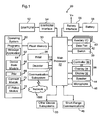
- the portable electronic device 20 includes a number of components such as the main processor 22 that controls the overall operation of the portable electronic device 20. Communication functions, including data and voice communications, are performed through a communication subsystem 24. Data received by the portable electronic device 20 can be decompressed and decrypted by a decoder 26, operating according to any suitable decompression techniques (e.g. YK decompression, and other known techniques) and encryption techniques (e.g. using an encryption technique such as Data Encryption Standard (DES), Triple DES, or Advanced Encryption Standard (AES)). In some examples, the communication subsystem 24 receives messages from and send messages to a wireless network 1000.
- a decompression techniques e.g. YK decompression, and other known techniques
- encryption techniques e.g. using an encryption technique such as Data Encryption Standard (DES), Triple DES, or Advanced Encryption Standard (AES)
- DES Data Encryption Standard
- Triple DES Triple DES
- AES Advanced Encryption Standard
- the communication subsystem 24 is configured in accordance with the Global System for Mobile Communication (GSM) and General Packet Radio Services (GPRS) standards.
- GSM Global System for Mobile Communication
- GPRS General Packet Radio Services
- the GSM/GPRS wireless network is used worldwide. New standards such as Enhanced Data GSM Environment (EDGE) and Universal Mobile Telecommunications Service (UMTS) are believed to have similarities to the network behavior described herein, and it will also be understood by persons skilled in the art that the embodiments described herein may use any other suitable standards that are developed in the future.
- the wireless link connecting the communication subsystem 24 with the wireless network 1000 in some examples, represents one or more different Radio Frequency (RF) channels, operating according to defined protocols specified for GSM/GPRS communications. With newer network protocols, these channels may be capable of supporting both circuit switched voice communications and packet switched data communications.
- RF Radio Frequency
- wireless network 1000 associated with the portable electronic device 20 is a GSM/GPRS wireless network in one example implementation
- other wireless networks are associated with the portable electronic device 20 in other examples.
- the different types of wireless networks that may be employed include, for example, data-centric wireless networks, voice-centric wireless networks, and dual-mode networks that can support both voice and data communications over the same physical base stations.
- Combined dual-mode networks include, but are not limited to, Code Division Multiple Access (CDMA) or CDMA1000 networks, GSM/GPRS networks (as mentioned above), and future third-generation (3G) networks like EDGE and UMTS.
- CDMA Code Division Multiple Access
- 3G Third-generation
- Some other examples of data-centric networks include Wi-Fi TM or other IEEE 802.11 network, MobitexTM and DataTACTM network communication systems.
- the main processor 22 interacts with additional subsystems such as a Random Access Memory (RAM) 28, a flash memory 30, a display 32 with a touch-sensitive overlay 34 connected to an electronic controller 36 that together make up a touch-sensitive display 38, a tactile mechanism 39, an auxiliary input/output (I/O) subsystem 40, a data port 42, a speaker 44, a microphone 46, short-range communications 48 and other device subsystems 50.
- RAM Random Access Memory
- I/O auxiliary input/output
- the touch-sensitive overlay 34 and the electronic controller 36 provide a touch-sensitive input device and, in some examples, the main processor 22 interacts with the touch-sensitive overlay 34 via the electronic controller 36.
- some of the subsystems of the portable electronic device 20 perform communication-related functions, whereas other subsystems provide "resident" or on-device functions.
- the display 32 and the touch-sensitive overlay 34 are used for both communication-related functions, such as entering a text message for transmission over the network 1000, and device-resident functions such as a calculator or task list.
- the portable electronic device 20 can send and receive communication signals over the wireless network 1000 after network registration or activation procedures have been completed.
- network access is associated with a subscriber or user of the portable electronic device 20.
- the portable electronic device 20 uses a SIM/RUIM card 52 (i.e. Subscriber Identity Module or a Removable User Identity Module) inserted into a SIM/RUIM interface 54 for communication with a network such as the network 1000.
- SIM/RUIM card 52 is one type of a conventional "smart card" that can be used to identify a subscriber of the portable electronic device 20 and to personalize the portable electronic device 20, among other things.
- the portable electronic device 20 is not fully operational for communication with the wireless network 1000 without the SIM/RUIM card 52.
- the SIM/RUIM card 52 By inserting the SIM/RUIM card 52 into the SIM/RUIM interface 54, a subscriber can access all subscribed services. Examples of services include: web browsing and messaging such as e-mail, voice mail, Short Message Service (SMS), and Multimedia Messaging Services (MMS). Examples of more advanced services include: point of sale, field service and sales force automation.
- the SIM/RUIM card 52 includes a processor and memory for storing information. Once the SIM/RUIM card 52 is inserted into the SIM/RUIM interface 54, it is coupled to the processor 22.
- the SIM/RUIM card 52 can include some user parameters such as an International Mobile Subscriber Identity (IMSI).
- IMSI International Mobile Subscriber Identity
- An advantage of using the SIM/RUIM card 52 is that a subscriber is not necessarily bound by any single physical portable electronic device.
- the SIM/RUIM card 52 stores additional subscriber information for a portable electronic device as well, including datebook (or calendar) information and recent call information.
- user identification information can also be programmed into the flash memory 30.
- the portable electronic device 20 is a battery-powered device and includes a battery interface 56 for receiving one or more rechargeable batteries 58.
- the battery 58 is a smart battery with an embedded microprocessor.
- the battery interface 56 is coupled to a regulator (not shown), which assists the battery 58 in providing power V+ to the portable electronic device 20.
- a regulator not shown
- future technologies such as micro fuel cells may provide the power to the portable electronic device 20.
- the portable electronic device 20 also includes an operating system 60 and software components 62 to 72 which are described in more detail below.
- the operating system 60 and the software components 62 to 72 that are executed by the main processor 22 are typically stored in a persistent store such as the flash memory 30, which, in other examples, is alternatively a read-only memory (ROM) or similar storage element (not shown).
- ROM read-only memory
- portions of the operating system 60 and the software components 62 to 72, such as specific device applications, or parts thereof, are temporarily loaded into a volatile store such as the RAM 28.
- Other software components can also be included, as is well known to those skilled in the art.
- the subset of software applications 62 that control basic device operations, including data and voice communication applications, in some examples, are installed on the portable electronic device 20 during its manufacture.
- Other software applications include a message application 64 that can be any suitable software program that allows a user of the portable electronic device 20 to send and receive electronic messages.
- a message application 64 can be any suitable software program that allows a user of the portable electronic device 20 to send and receive electronic messages.
- Messages that have been sent or received by the user are typically stored in the flash memory 30 of the portable electronic device 20 or some other suitable storage element in the portable electronic device 20.
- some of the sent and received messages are stored remotely from the device 20 such as in a data store of an associated host system that the portable electronic device 20 communicates with.
- the software applications 62 can further include a device state module 66, a Personal Information Manager (PIM) 68, and other suitable modules (not shown).
- the device state module 66 provides persistence, i.e. the device state module 66 ensures that important device data is stored in persistent memory, such as the flash memory 30, so that the data is not lost when the portable electronic device 20 is turned off or loses power.
- the PIM 68 includes functionality for organizing and managing data items of interest to the user, such as, but not limited to, e-mail, contacts, calendar events, voice mails, appointments, and task items.
- a PIM application in some examples, has the ability to send and receive data items via the wireless network 1000.
- PIM data items are seamlessly integrated, synchronized, and updated via the wireless network 1000 with the portable electronic device subscriber's corresponding data items stored and/or associated with a host computer system. This functionality creates a mirrored host computer on the portable electronic device 20 with respect to such items. This can be particularly advantageous when the host computer system is the portable electronic device subscriber's office computer system.
- the portable electronic device 20 also includes a connect module 70, and an information technology (IT) policy module 72.
- the connect module 70 implements the communication protocols that are required for the portable electronic device 20 to communicate with the wireless infrastructure and any host system, such as an enterprise system, that the portable electronic device 20 is authorized to interface with.
- the connect module 70 includes a set of APIs that can be integrated with the portable electronic device 20 to allow the portable electronic device 20 to use any number of services associated with the enterprise system.
- the connect module 70 allows the portable electronic device 20 to establish an end-to-end secure, authenticated communication pipe with the host system.
- a subset of applications for which access is provided by the connect module 70 can be used to pass IT policy commands from the host system to the portable electronic device 20. This can be done in a wireless or wired manner.
- These instructions can then be passed to the IT policy module 72 to modify the configuration of the device 20.
- the IT policy update can also be done over a wired connection.
- software applications can also be installed on the portable electronic device 20.
- These software applications can be third party applications, which are added after the manufacture of the portable electronic device 20. Examples of third party applications include games, calculators, utilities, etc.
- the additional applications can be loaded onto the portable electronic device 20 through at least one of the wireless network 1000, the auxiliary I/O subsystem 40, the data port 42, the short-range communications subsystem 48, or any other suitable device subsystem 50.
- This flexibility in application installation has the potential to increase the functionality of the portable electronic device 20 and to provide enhanced on-device functions, communication-related functions, or both.
- secure communication applications in some cases, enable electronic commerce functions and other such financial transactions to be performed using the portable electronic device 20.
- the data port 42 enables a subscriber to set preferences through an external device or software application and extends the capabilities of the portable electronic device 20 by providing for information or software downloads to the portable electronic device 20 other than through a wireless communication network.
- the alternate download path in some examples, is used to load an encryption key onto the portable electronic device 20 through a direct and thus reliable and trusted connection to provide secure device communication.
- the data port 42 can be any suitable port that enables data communication between the portable electronic device 20 and another computing device.
- the data port 42 can be a serial or a parallel port.
- the data port 42 can be a USB port that includes data lines for data transfer and a supply line that can provide a charging current to charge the battery 58 of the portable electronic device 20.
- the short-range communications subsystem 48 provides for communication between the portable electronic device 20 and different systems or devices, without the use of the wireless network 1000.
- the short-range communications subsystem 48 includes an infrared device and associated circuits and components for short-range communication. Examples of short-range communication standards include standards developed by the Infrared Data Association (IrDA), Bluetooth, and the 802.11 family of standards developed by IEEE.
- IrDA Infrared Data Association
- Bluetooth Bluetooth
- a received signal such as a text message, an e-mail message, or web page download is processed by the communication subsystem 24 and input to the main processor 22.
- the main processor 22 processes the received signal for output to the display 32 or alternatively to the auxiliary I/O subsystem 40.
- a subscriber can also compose data items, such as e-mail messages, for example, using the touch-sensitive overlay 34 on the display 32 that are part of the touch-sensitive display 38, and possibly the auxiliary I/O subsystem 40.
- the auxiliary I/O subsystem 40 includes devices such as: a mouse, track ball, optical navigation module, infrared fingerprint detector, or a roller wheel with dynamic button pressing capability.
- a composed item is transmitted over the wireless network 1000 through the communication subsystem 24.
- the overall operation of the portable electronic device 20, in some examples, is substantially similar, except that the received signals are output to the speaker 44, and signals for transmission are generated by the microphone 46.
- Alternative voice or audio I/O subsystems such as a voice message recording subsystem, can also be implemented on the portable electronic device 20.
- voice or audio signal output are accomplished primarily through the speaker 44 in some examples, the display 32 can also be used to provide additional information such as the identity of a calling party, duration of a voice call, or other voice call related information.
- FIG. 2A shows a front view of an example portable electronic device 20 in portrait orientation.
- the portable electronic device 20 includes a housing 74 that houses the internal components that are shown in FIG. 1 and frames the touch-sensitive display 38 such that the touch-sensitive display 38 is exposed for user-interaction therewith when the portable electronic device 20 is in use.
- the touch-sensitive display 38 includes a portrait mode virtual keyboard 76 for user entry of data in the form of, for example, text during operation of the portable electronic device 20. It will be appreciated that such a virtual keyboard 76, in some examples, is used for data entry in any suitable application such as in an electronic mail application, during electronic mail composition or in any other suitable application.
- the portrait mode virtual keyboard 76 of FIG. 2A is provided for data entry in an Internet browser application and is shown as a reduced keyboard for example purposes.
- the present disclosure is not limited to the portrait mode virtual keyboard 76 shown, as other keyboards including other reduced keyboards or full keyboards are possible.
- suitable keyboards include full or reduced QWERTY keyboards, full or reduced Dvorak keyboards, and other full or reduced keyboards, including keyboards adapted for non-Roman text input, such as Korean, Chinese or Japanese text input.
- the touch-sensitive display 38 is any suitable touch-sensitive display 38 such as a capacitive touch-sensitive display.
- a capacitive touch-sensitive display 38 includes the display device, such as an LCD display 32 and the touch-sensitive overlay 34, in the form of a capacitive touch-sensitive overlay 34, as shown in FIG. 2B .
- the capacitive touch-sensitive overlay 34 includes a number of layers in a stack.
- the layers include, for example, a substrate 181 fixed by a suitable adhesive (not shown), a ground shield layer 182, a barrier layer 184, a pair of capacitive touch sensor layers including an outer capacitive touch sensor layer 186a and an inner capacitive touch sensor layer 186b separated by a substrate or other barrier layer 188, and a cover layer 190 fixed to the outer capacitive touch sensor layer 186a by a suitable adhesive (not shown).
- the capacitive touch sensor layers are made of any suitable material such as patterned indium tin oxide (ITO).
- the housing 74 includes a back 302, a frame 78, which frames the touch-sensitive display 38, sidewalls 306 that extend between and are generally perpendicular to the back 302 and the frame 78, and a base 304 that is spaced from and generally parallel to the back 302.
- the base 304 can be any suitable base and can include, for example, a printed circuit board or flex circuit board.
- the back 302 includes a plate (not shown) that is releasably attached for insertion and removal of, for example, the battery 58 and the SIM/RUIM card 52 described above. It will be appreciated that the back 302, the sidewalls 306 and the frame 78 can be injection molded, for example. In the example portable electronic device 20 shown in FIG. 2A , the frame 78 is generally rectangular with rounded corners although other shapes are possible.
- the display 32 and the touch-sensitive overlay 34 can be supported on a support tray 308 of suitable material such as magnesium for providing mechanical support to the display 32 and touch-sensitive overlay 34.
- the display 32 and touch-sensitive overlay 34 are biased away from the base 304, toward the frame 78 by biasing elements 310 such as gel pads between the support tray 308 and the base 304.
- Compliant spacers 312, which can also be in the form of gel pads for example, are located between an upper portion of the support tray 308 and the frame 78.
- the touch-sensitive display 38 is moveable within the housing 74 as the touch-sensitive display 38 can be moved toward the base 304, thereby compressing the biasing elements 310.
- the touch-sensitive display 38 can also be pivoted within the housing 74 with one side of the touch-sensitive display 38 moving toward the base 304, thereby compressing the biasing elements 310 on the same side of the touch-sensitive display 38 that moves toward the base 304.
- the tactile mechanism 39 is supported on one side of the base 304, which can be a printed circuit board, while the opposing side provides mechanical support and electrical connection for other components (not shown) of the portable electronic device 20.
- the tactile mechanism 39 can be located between the base 304 and the support tray 308.
- the tactile mechanism 39 for example a piezoelectric assembly, in some examples is located in any suitable position to provide adequate tactile feedback to an interaction with the touch-sensitive display 38.
- the tactile mechanism 39 is in contact with the support tray 308.
- actuation of the tactile mechanism 39 for example by a displacement towards or away from the touch sensitive display 38, is able to provide the user with a positive tactile feedback during user interaction with the user interface of the portable electronic device 20.
- the tactile mechanism 39 in some examples is actuated in response to a signal, for example from the processor 22, which in turn is in response to a physical force sensed at the touch sensitive display 38, to indicate a user interaction.
- a signal for example from the processor 22, which in turn is in response to a physical force sensed at the touch sensitive display 38, to indicate a user interaction.
- a single tactile mechanism 39 is shown any suitable number of tactile mechanisms 39 can be used.
- a touch event is detected upon user touching of the touch-sensitive display 38.
- a touch event is determined upon a user touch at the touch-sensitive display 38 for selection of, for example, a feature in a list, such as a message or other feature for scrolling in the list or selecting a virtual input key.
- signals are sent from the touch-sensitive overlay 34 to the controller 36 when a suitable object such as a finger or other conductive object held in the bare hand of a user, is detected.
- the touch event is detected and an X and a Y location of the touch is determined.
- the X and Y location of the touch in some examples, is determined to fall within the touch-sensitive area defined by the boundary on the touch-sensitive display 38.
- the X and Y locations of a touch event are both determined, with the X location determined by a signal generated as a result of capacitive coupling with one of the touch sensor layers 186a, 186b and the Y location determined by the signal generated as a result of capacitive coupling with the other of the touch sensor layers 186a, 186b.
- each of the touch-sensor layers 186a, 186b provides a signal to the controller 36 as a result of capacitive coupling with a suitable object such as a finger of a user or a conductive object held in a bare hand of a user resulting in a change in the electric field of each of the touch sensor layers.
- the outer touch sensor layer 186a is connected to a capacitive touch screen controller 192 in the portable electronic device 20 for conducting a continuous electrical current across the inner touch sensor layer 186b and detecting a change in the capacitance as a result of capacitive coupling between, for example, the finger of a user or a conductive stylus held by a user, and the outer touch sensor layer 186a.
- the change in capacitance acts as a signal to the capacitive touch screen controller 192, which senses the touch or near touch, on the touch-sensitive display 38.
- capacitive touch sensitive overlay 34 When a user places a finger, or other conductive object (e.g., a conductive stylus) on capacitive touch sensitive overlay 34 without applying force to cause the outer and inner touch sensor layers 186a, 186b to contact each other, capacitive coupling of the finger or conductive object with the outer touch sensor layer 186a occurs, resulting in a signal at the capacitive touch screen controller 192. Capacitive coupling also occurs through the cover layer 190 and through a small air gap (not shown).
- a finger, or other conductive object e.g., a conductive stylus
- capacitive coupling occurs, resulting in a signal being sent to the capacitive touch screen controller 192, when the finger or other conductive object (e.g., held in the bare hand of a user) approaches the surface of the cover layer 190 and when contacting the cover layer 190, prior to force being applied to the cover layer 190 to force the outer and inner touch sensor layers 186a, 186b into contact with each other.
- the sensitivity of the capacitive touch screen controller 192 can therefore be set to detect an approaching finger (or other conductive object) at a small distance away from the cover layer 190 of, for example, 9 millimeters (mm) or less.
- the location of approach is not determined, however the approach of a finger or other conductive object that is proximal the outer touch sensor layer 186a is determined.
- the outer touch sensor layer 186a and the capacitive touch screen controller 192 act to detect proximity, detecting a finger or conductive object proximal the surface of the cover layer 190.
- the signals represent the respective X and Y touch location values. It will be appreciated that other attributes of the user's touch on the capacitive touch sensitive overlay 34 can be determined. For example, the size and the shape of the touch on the capacitive touch sensitive overlay 34 can be determined in addition to the location (e.g., X and Y values) based on the signals received at the controller 36 from the touch sensor layers 186a, 186b.
- a user's touch on the capacitive touch sensitive overlay 34 is determined by determining the X and Y touch locations and user-selected input is determined based on the X and Y touch locations and the application executed by the processor 22. For example, this determination is carried out by the processor 22 using one or more software modules 62, including the specific application being executed.
- the application provides the virtual keyboard 76 having a plurality of virtual input keys or buttons, which can be selected by the user.
- the user selected virtual input key in an example, is matched to the X and Y touch location.
- the button selected by the user is determined based on the X and Y touch location and the application.
- the user is able to text via the virtual keyboard 76, selecting characters or symbols associated with the virtual input keys, such as alphanumeric characters from the virtual keyboard 76, by touching the touch-sensitive display at the location of the characters corresponding to the virtual input keys of the virtual keyboard 76.
- the text or data entry is accomplished by a "click to enter" operation.
- the character or symbol is entered by depressing the virtual input key on the capacitive touch sensitive overlay 34 with sufficient force to overcome the bias of the capacitive touch sensitive overlay 34, to cause movement of the touch-sensitive display 38.
- the selection of the virtual input key 80 results in signals that may be received by the main processor 22, thereby entering the corresponding character or symbol for rendering on the touch-sensitive display.
- the processor 22 in some examples, also correspondingly sends a signal to the tactile mechanism 39 to flex inwards or outwards, for example in the case of a piezoelectric assembly, to provide a tactile feedback to the user.
- the "click to enter" operation thus is able to provide a tactile feedback confirming the entry to the user, thereby reducing the chance of inadvertent double entry requiring correction. For example, this has the potential to also reduce the need for additional user interaction and use time, thereby reducing battery consumption.
- the click entry has the potential to also allow the user to touch the device and ensure the correct character or symbol is selected before entry of that character or symbol by clicking.
- the characters are alphanumeric characters, although other characters are also possible, such as characters for non-English languages.
- the main processor 22 receives a user-selection of an Internet browser application for browsing the Internet by, for example, determination of a touch event at an Internet browser icon (not shown) displayed on the touch-sensitive display 38.
- the virtual keyboard 76 in the example shown in FIG. 2A , is rendered in the portrait mode.
- Devices such as accelerometers, can be used to determine the relative orientation of the portable electronic device 20 and change the orientation of the touch-sensitive display accordingly.
- the virtual input keys or buttons 80 are rendered with the alphanumeric characters and other keyboard buttons displayed in an upright position for the user.
- the portable electronic device 20 can be operated in any suitable mode for determining a user-desired one of the letters upon determination of a touch event at the respective one of the virtual input keys or buttons 80 of the virtual keyboard 76.
- letters can be selected using a single-tap mode, multi-tap mode, a text prediction mode or using any other suitable mode.
- the portable electronic device 20 also includes four physical buttons 82, 84, 86, 88 in the housing 74 for user-selection for performing functions or operations including an "off-hook" button 82 for placing an outgoing cellular telephone call or receiving an incoming cellular telephone call, a Menu button 84 for displaying a context-sensitive menu or submenu, an escape button 86 for returning to a previous screen or exiting an application, and an "on-hook” button 88 for ending a cellular telephone call.
- the remainder of the buttons shown on the face of the example portable electronic device of FIG. 2A are virtual buttons or input keys 80 on the touch-sensitive display 38. However, it is also appreciated that the buttons 82, 84, 86 and 88 could also be virtual buttons, similar to the virtual input keys 80 described above.
- a display area is rendered, which in the present example is a portrait mode display area 90 that is a portrait mode Internet browser display screen 92.
- the display area is provided in the portrait mode as a result of determination of the orientation at the accelerometer (not shown).
- the display area is rendered above the portrait mode virtual keyboard 76 when the portable electronic device 20 is in the portrait orientation.
- data input received from the virtual keyboard 76 is rendered in a data entry field 94 of the Internet browser display screen 92.
- input is received in the form of user selection of characters or symbols by touching the virtual buttons or input keys 80 so as to select the desired character or symbol associated with the virtual button or input key 80 in either the portrait mode or landscape mode.
- the user enters "http://www.xyz.c" and the data received is displayed in the data entry field 94 of the portrait mode Internet browser display screen 92.
- the user when entering data, the user is able to turn the portable electronic device 20 to a different orientation to provide a different keyboard layout such as to change from a reduced keyboard layout in the portrait orientation to a full keyboard layout in the landscape orientation, as in the present example.
- the user is able to also choose to turn the portable electronic device 20 to provide a different display area for the application.
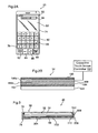
- FIG. 4 showing a piezoelectric assembly 400 in an exploded schematic.
- the piezoelectric assembly 400 comprises a first electrode 402 and a second electrode 404.
- the first electrode 402 and the second electrode 404 are spaced apart from each other.
- the first electrode 402 is in electrical communication with a power source, such as a current or voltage source.
- the second electrode 404 is in electrical communication with a reference source (e.g., a ground source).
- a power source such as a current or voltage source.
- the second electrode 404 is in electrical communication with a reference source (e.g., a ground source).
- electrical power such as an electrical signal
- the first and second electrodes 402, 404 are disc-shaped, although any suitable geometry is possible.
- the first electrode 402 has a diameter of about 13 mm and the second electrode 404 has a diameter of about 13 mm, although other sizes and shapes may be appropriate.
- the first and second electrodes 402, 404 are made of any suitable electrically conductive material that accommodates flexing or displacement in the piezoelectric assembly, for example a silver material.
- a piezoelectric element 406 is disposed between the first and second electrodes 402, 404 and is in electrical communication with each of the first and second electrodes 402, 404.
- the piezoelectric element 406 is made from a piezoelectric material such as a piezoelectric ceramic, for example, lead zirconate titanate (PZT).
- PZT lead zirconate titanate
- the electrical communication between the piezoelectric element 406 and the first and second electrodes 402, 404 is provided through direct contact.
- the piezoelectric element 406 may be designed to match the geometries of the first and second electrodes 402, 404, for example by being disc-shaped.
- the piezoelectric element 406 has a diameter of about 13 mm and is about 0.1 mm thick.
- the piezoelectric element 406 has an unactuated state and an actuated state. In the absence of an electric field, the piezoelectric element 406 exhibits the unactuated state. For example, the piezoelectric element 406 may have an unflexed or unexpanded condition in the absence of the electric field. In the presence of an electrical field generated between the first and second electrodes 402, 404, for example when an electric field is generated between the first and the second electrodes 402, 404, the piezoelectric element 406 exhibits an actuated state. For example, the piezoelectric element 406 may have a flexed or expanded condition in the presence of an electric field.
- the first and second electrodes 402, 404 are bonded directly to the piezoelectric element 406, for example by silk-screening thin (e.g., 1-5 microns thick) silver first and second electrodes 402, 404 on opposing surfaces of the piezoelectric element 406.
- the first and second electrodes 402, 404 and the piezoelectric element 406 together form an electrode assembly 420.
- the piezoelectric assembly 400 is in electrical communication (e.g., for receiving or transmitting signals) with other components of the electronic device 20 via electrical connectors.
- the piezoelectric assembly 400 includes a signal electrical connector 408 and a reference electrical connector 410.
- the signal electrical connector 408 is in electrical communication with the first electrode 402, for example through contact engagement with the first electrode 402, to provide electrical communication between the first electrode 402 and a current or voltage source.
- the reference electrical connector 410 is in electrical communication with the second electrode 404, for example through contact engagement with the second electrode 404, to provide electrical communication between the second electrode 404 and a reference source.
- the signal electrical connector 408 and the reference electrical connector 410 are, in turn, connected to or extensions from other components of the electrical device 20, such as other circuits.
- One of the signal electric connector 408 or the reference electrical connector 410 includes a metal shim.
- the signal electrical connector 408 is a form of metal shim.
- the signal electrical connector 408 is a conductive metal disc about 20 mm in diameter (although other sizes may be appropriate), and is coupled to the first electrode 402 by a conductive adhesive 409, such as a conductive acrylic epoxy disc about 15 mm in diameter and 0.01 mm in thickness, although other materials with similar properties and other sizes may be suitable.
- the disc of the signal electrical connector 408 and reference electrical connector 410 may each be any suitable electrically conductive material, such as a nickel alloy, and is suitably thick to provide support for the piezoelectric assembly 400.
- the disc of the signal electrical connector 408 and reference electrical connector 410 is about 0.10 mm to about 0.15 mm thick, with a diameter of about 20 mm, although other sizes may be suitable.
- the signal electrical connector 408 and reference electrical connector 410 is designed to optimize or improve the mechanical response of the piezoelectric assembly 400, for example by providing robustness while allowing the piezoelectric element 406 to actuate or flex.
- the reference electrical connector 410 is a flexible printed circuit board (PCB) disc about 18 mm in diameter, and is coupled to the second electrode 404 by a conductive adhesive 411, such as a conductive acrylic epoxy disc about 13 mm in diameter.
- a conductive adhesive 411 such as a conductive acrylic epoxy disc about 13 mm in diameter.
- Alternative materials with similar properties may be utilized and that reference electrical connector 410 and conductive adhesive 411 may have alternate dimensions to suit the application in other embodiments.
- the flexible PCB comprises electronic devices or circuits (e.g., silver circuits) on a flexible plastic substrate.
- the substrate is a flexible polymer such as polyimide, PEEK or polyester.
- the signal and reference electrical connectors 408, 410 are made of a material that is more resistant to fatigue than the first and second electrodes 402, 404 and the piezoelectric element 406.
- Electrode assembly 420 When exposed to high humidity and high voltages (e.g., high AC voltages), there is a potential for the electrode assembly 420 to experience an electrical short failure.
- This electrical short can be induced by the migration of conductive material (e.g., silver) through the piezoelectric element 406 from the first electrode 402 (e.g., a positive electrode) to the second electrode 404 (e.g., a negative electrode).
- conductive material e.g., silver
- the signal electrical connector 408 extends over and covers a side surface of the first electrode 402 which is opposite to a side surface of the first electrode 402 which is disposed in contact engagement with the piezoelectric element 406 (to thereby effect the electrical communication between the first electrode 402 and the piezoelectric element 406).
- the side surface over which the signal electrical connector 408 extends over and covers is at least 50% of the area of the side surface of the first electrode 402 which is opposite to the side surface of the first electrode 402 which is disposed in contact engagement with the piezoelectric material.
- the reference electrical connector 410 extends over and covers a side surface of the second electrode 404, which is opposite to a side surface of the second electrode 404 which is disposed in contact engagement with the piezoelectric element 406 (to thereby effect the electrical communication between the second electrode 404 and the piezoelectric element 406).
- the side surface over which the reference electrical connector 410 extends over and covers is at least 50% of the area of the side surface of the second electrode 404, which is opposite to the side surface of the second electrode 404 that is disposed in contact engagement with the piezoelectric material.
- the piezoelectric assembly 400 includes a spacer 426 positioned about the perimeter of the electrode assembly 420.
- the spacer 426 is disposed between the signal and reference electrical connectors 408, 410 such that no electrical communication is provided between the signal electrical connector 408 and the reference electrical connector 410 through the spacer 426.
- the spacer 426 forms a full ring about the perimeter of the electrode assembly 420 and is coupled to the signal and reference electrical connectors 408, 410 about the full perimeter of the electrode assembly 420.
- the spacer 426 is a non-conductive adhesive, such as a non-conductive adhesive tape, having an inner diameter of about 16 mm and an outer diameter of about 18 mm, and is coupled to each of the signal and reference electrical connectors 408, 410.
- the spacer 426 in this example, is an annulus that is larger than the electrode assembly 420 but smaller than the signal and reference electrical connectors 408, 410. Although the spacer 426 is shown as an annulus, in some examples, the spacer 426 is not a full annulus, and contains one or more notches or gaps.
- the electrode assembly 420 is disposed between the signal electrical connector 408, the reference electrical connector 410 and the spacer 426.
- the signal electrical connector 408, the reference electrical connector 410 and the spacer 426 together define a humidity barrier space within which the electrode assembly 420 is disposed.
- the signal and reference electrical connectors 408, 410 and the spacer 426 are disposed in close contact with each other, forming a humidity barrier space with a substantially water-tight seal.
- the disposition of the electrode assembly 420 within the humidity barrier space helps to reduce the potential for humidity to reach the electrode assembly 420, thus helping to reduce the potential for migration of conductive material between the first and second electrodes 402, 404. This helps to increase the reliability and performance of the piezoelectric assembly 400.
- a signal source 428 is coupled to the signal electrical connector 408, such as by laser soldering.
- a reference source 430 is coupled to the reference electrical connector 410, such as by laser soldering, or by being formed integrally with the reference electrical connector 410.
- the disclosed piezoelectric assembly 400 avoids the need to provide an additional humidity barrier, such as a silicone conformal coating, which in some cases requires increased infrastructure, assembly, time and overall cost during manufacturing.
- an additional humidity barrier such as a silicone conformal coating
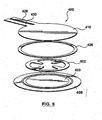
- FIG. 5 showing an exploded schematic of another example embodiment of the piezoelectric assembly 400.
- one or both of the signal and reference electrical connectors 408, 410 is coupled to the electrode assembly 420 via a conductive adhesive 502.
- the conductive adhesive 502 is provided between the reference electrical connector 410 and the electrode assembly 420. It should be understood that in some examples the conductive adhesive 502 can be provided between the signal electrical connector 408 and the electrode assembly 420, or between both the signal and reference electrical connectors 408, 410 and the respective surface of the electrode assembly 420.
- the conductive adhesive 502 is designed to be in contact engagement with a portion of the peripheral surface area of the first electrode 402, thereby maintaining contact with all portions of the first electrode 402, even in the presence of cracking.
- peripheral surface area it is meant the surface area of the first electrode 402 that is adjacent or substantially adjacent to the periphery of the first electrode 402, and is not necessarily limited to surface areas directly adjacent to the periphery of the first electrode 402.
- the conductive adhesive 502 is designed with a piezoelectric material-accommodating space for accommodating actuation of the piezoelectric element 406.
- This piezoelectric material-accommodating space has the potential to reduce the rigidity of the piezoelectric assembly 400, thus reducing the work required for the piezoelectric element 406 to actuate and thereby allowing an increased response and increased tactile feedback.
- the conductive adhesive 502 further includes one or more surfaces extending inwards from the periphery of the first electrode 402 for contact engagement with the first electrode 402.
- the conductive adhesive 502 includes, for example, four extensions extending radially inwards.
- Such a design has the potential to be useful for increasing the area of contact engagement between the conductive adhesive 502 and the first electrode 402.
- An increased contact engagement area has the potential to improve electrical communication between the signal electrical connector 408 and the first electrode 402.
- an increased contact engagement area has the potential to provide a more robust electrical and physical contact.
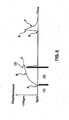
- FIG. 6 is a chart illustrating the displacement of an example embodiment of the piezoelectric assembly 400 in operation.
- the piezoelectric assembly 400 is used as the tactile mechanism 39 described above.
- the piezoelectric assembly 400 does not receive a signal, in some examples there is no electric field generated between the first and second electrodes 402, 404, and the piezoelectric element 406 is in its unactuated state.
- the piezoelectric element 406 in this example is concave downwards from the general plane formed by its peripheral edge such that it is concave away from the touch-sensitive display 38, causing a corresponding configuration of the piezoelectric assembly 400.
- the piezoelectric assembly 400 receives a signal, for example from the processor 22, causing the generation of an electric field between the first and second electrodes 402, 404 and a subsequent change of the piezoelectric element 406 to its actuated state, which in this example brings the piezoelectric element 406 (and by extension the piezoelectric assembly 400) to be substantially planar with its peripheral edge and substantially flush or in contact with the touch sensitive display 38.
- This change to the actuated state typically occurs gradually enough to be unnoticeable by a user, as shown by the gradual rise (B).
- the piezoelectric assembly 400 exhibits a displacement of about 100 microns over about 20 ms from the unactuated to the actuated state.
- the touch input at the touch sensitive display 38 exerts further force on the touch sensitive display 38, the force sensed by the touch sensitive display 38 increases until a predetermined threshold is reached at (3) and the touch input is determined to be a full touch input.
- the signal to the piezoelectric assembly 400 is stopped, causing the dissipation of the generated electric field between the first and second electrodes 402, 404 and a subsequent change of the piezoelectric element 406 back to its unactuated state (and by extension the piezoelectric assembly 400), which in this example is concaved away from the touch sensitive display 38.
- the change back to the unactuated state typically is relatively rapid so that the user feels the change, as shown by the sharp drop (C).
- the piezoelectric assembly 400 exhibits a displacement of about 100 microns over about 3ms from the actuated to the unactuated state.
- the piezoelectric assembly 400 For the duration that the full touch input is maintained on the touch sensitive display 38, the piezoelectric assembly 400 remains unactuated. At (D) the touch input is removed, and this is sensed by the touch sensitive display 38. When the removal of the touch input is determined, a signal is sent to the piezoelectric assembly 400, again generating the electric field between the first and second electrodes 402, 404 and a subsequent change of the piezoelectric element 406 to its actuated state (and by extension the piezoelectric assembly 400), substantially flush with the touch sensitive display 38. Typically, this occurs relatively rapidly, such that the change is felt by the user, as shown by the sharp rise (D). In this example, the piezoelectric assembly 400 exhibits a displacement of about 100 microns over about 3ms from the unactuated to the actuated state.
- the signal to the piezoelectric assembly 400 is stopped, causing the generated electric field between the first and second electrodes 402, 404 to dissipate and thus the return of the piezoelectric material 406 to its unactuated state (and by extension the piezoelectric assembly 400).
- the piezoelectric assembly 400 typically exhibits a gradual return to the unactuated state, as shown by the gradual drop (F). In this example, the piezoelectric assembly 400 gradually returns to its unactuated state over about 15 ms.
- a user using a touch input on the touch sensitive display 38 initially feels a resistance in response to an initial touch input, as the piezoelectric assembly 400 changes to its substantially planar actuated state.
- the user feels a give or clicking sensation, as the piezoelectric assembly 400 returns to its concave unactuated state.
- the touch input is released, the user feels an upwards clicking sensation, as the piezoelectric assembly 400 changes to its actuated state again, before finally relaxing back to its unactuated state. This behaviour has the potential to be useful to provide tactile feedback for the touch-sensitive display 38.
- the piezoelectric assembly 400 has been described in certain variations and examples, the variations and examples described can be combined, and the piezoelectric assembly 400 can have a combination of any of the variations described.
- the signal electrical connector 408 is described as receiving a signal from a current or voltage source and communicating the signal to the first electrode 402
- the reference electrical connector 410 and second electrode 404 are described as being in electrical communication with a reference source, the roles signal and reference can be reversed, such that the first electrode 402 is in electrical communication with the reference source and the second electrode 404 is in electrical communication with the current or voltage source to receive a signal.
Abstract
Description
- The present disclosure relates generally to piezoelectric assemblies. In particular, the present disclosure relates to piezoelectric assemblies suitable for electronic devices including devices having a touch sensitive display.
- Electronic devices, including portable electronic devices, have gained widespread use and can provide a variety of functions including, for example, telephonic, electronic messaging and other personal information manager (PIM) application functions. Portable electronic devices can include several types of devices including mobile stations such as simple cellular telephones, smart telephones, wireless PDAs, and laptop computers with wireless 802.11 or Bluetooth capabilities. These devices run on a wide variety of networks from data-only networks such as Mobitex and DataTAC to complex voice and data networks such as GSM/GPRS, CDMA, EDGE, UMTS and CDMA2000 networks.
- Such devices often employ a touch sensitive display. A tactile mechanism is typically incorporated into the touch sensitive display to provide a tactile feedback when a user interacts with the touch sensitive display. For example, there may be a mechanical switch incorporated into the touch sensitive display to mimic the feel of a physical keyboard. Other mechanisms may use a piezoelectric assembly that provides tactile feedback.
EP 1 329 963 A1 relates to a device for reducing vibrations in a motor vehicle, which comprises a two-layered protective cover on a piezoelectric element which is mounted on a structure whose vibrations are to be used. The purpose of such cover is to insulate the piezoelectric element from its surroundings.
EP 2 079 115 A2
WO 2009/041564 relates to a piezoelectric transducer element composed of a base body having a movable section and a fixed section connected to the movable section; a lower electrode formed on the surface of the base body; a piezoelectric body formed on the lower electrode; and an upper electrode formed on the upper surface of the piezoelectric body. A surface exposed to the external of the upper electrode is covered with a water-repellent thin film.
"A vertically integrated media-isolated absolute pressure sensor", by K. Goldman et al., in Sensors and Actuators A 66 (1998) 155-159 relates to a media-isolated, temperature-compensated, bulk-micromachined integrated absolute pressure sensor. The device consists of two dice bonded together. Devices are batch fabricated by bonding two wafers together prior to sawing. The bottom wafer contains bulk-micromachined piezoresistive pressure sensors and the top wafer contains signal-conditioning integrated circuitry. The pressure sensors and the integrated circuits are coupled together by wirebonding from the top die down to the bottom die through via holes anisotropically etched in the top wafer. - Embodiments of the present disclosure will now be described, by way of example only, with reference to the attached Figures, wherein:
-
FIG. 1 is a block diagram of a portable electronic device according to an example; -
FIG. 2A is a front view of an example portable electronic device shown in a portrait orientation; -
FIG. 2B shows a cutaway view of an example touch-sensitive display of the portable electronic device ofFIG. 1 ; -
FIG. 3 is a simplified sectional side view of the portable electronic device ofFIG. 2A (not to scale); -
FIG. 4 is an exploded schematic of an example embodiment of a piezoelectric assembly; -
FIG. 5 is an exploded schematic of another example embodiment of a piezoelectric assembly; and -
FIG. 6 is a chart illustrating displacement of an example embodiment of a piezoelectric assembly in operation. - In accordance with one embodiment, there is provided a piezoelectric assembly as recited in claim 1.
- In accordance with another embodiment, there is provided a portable electronic device as recited in claim 15.
- The embodiments described herein generally relate to an electronic device including a touch-sensitive display. Examples of such electronic devices are portable electronic devices, including communication devices. Examples of portable electronic devices include mobile, or handheld, wireless communication devices such as pagers, cellular phones, cellular smart-phones, wireless organizers, personal digital assistants, wirelessly enabled notebook computers and the like.
- In some embodiments, the portable electronic device is a two-way communication device with advanced data communication capabilities including the capability to communicate with other portable electronic devices or computer systems through a network of transceiver stations. In some embodiments, the portable electronic device also has the capability to allow voice communication. Depending on the functionality provided by the portable electronic device, it may be referred to as a data messaging device, a two-way pager, a cellular telephone with data messaging capabilities, a wireless Internet appliance, or a data communication device (with or without telephony capabilities). In some embodiments, the portable electronic device is a portable device without wireless communication capabilities such as a handheld electronic game device, digital photograph album, digital camera and the like.
- Referring first to
FIG. 1 , there is shown therein a block diagram of an example embodiment of a portableelectronic device 20. The portableelectronic device 20 includes a number of components such as themain processor 22 that controls the overall operation of the portableelectronic device 20. Communication functions, including data and voice communications, are performed through acommunication subsystem 24. Data received by the portableelectronic device 20 can be decompressed and decrypted by adecoder 26, operating according to any suitable decompression techniques (e.g. YK decompression, and other known techniques) and encryption techniques (e.g. using an encryption technique such as Data Encryption Standard (DES), Triple DES, or Advanced Encryption Standard (AES)). In some examples, thecommunication subsystem 24 receives messages from and send messages to awireless network 1000. In this example embodiment of the portableelectronic device 20, thecommunication subsystem 24 is configured in accordance with the Global System for Mobile Communication (GSM) and General Packet Radio Services (GPRS) standards. The GSM/GPRS wireless network is used worldwide. New standards such as Enhanced Data GSM Environment (EDGE) and Universal Mobile Telecommunications Service (UMTS) are believed to have similarities to the network behavior described herein, and it will also be understood by persons skilled in the art that the embodiments described herein may use any other suitable standards that are developed in the future. The wireless link connecting thecommunication subsystem 24 with thewireless network 1000, in some examples, represents one or more different Radio Frequency (RF) channels, operating according to defined protocols specified for GSM/GPRS communications. With newer network protocols, these channels may be capable of supporting both circuit switched voice communications and packet switched data communications. - Although the
wireless network 1000 associated with the portableelectronic device 20 is a GSM/GPRS wireless network in one example implementation, other wireless networks are associated with the portableelectronic device 20 in other examples. The different types of wireless networks that may be employed include, for example, data-centric wireless networks, voice-centric wireless networks, and dual-mode networks that can support both voice and data communications over the same physical base stations. Combined dual-mode networks include, but are not limited to, Code Division Multiple Access (CDMA) or CDMA1000 networks, GSM/GPRS networks (as mentioned above), and future third-generation (3G) networks like EDGE and UMTS. Some other examples of data-centric networks include Wi-Fi™ or other IEEE 802.11 network, Mobitex™ and DataTAC™ network communication systems. Examples of other voice-centric data networks include Personal Communication Systems (PCS) networks like GSM and Time Division Multiple Access (TDMA) systems. In some examples, themain processor 22 interacts with additional subsystems such as a Random Access Memory (RAM) 28, aflash memory 30, adisplay 32 with a touch-sensitive overlay 34 connected to anelectronic controller 36 that together make up a touch-sensitive display 38, atactile mechanism 39, an auxiliary input/output (I/O)subsystem 40, adata port 42, aspeaker 44, amicrophone 46, short-range communications 48 andother device subsystems 50. The touch-sensitive overlay 34 and theelectronic controller 36 provide a touch-sensitive input device and, in some examples, themain processor 22 interacts with the touch-sensitive overlay 34 via theelectronic controller 36. - In some examples, some of the subsystems of the portable
electronic device 20 perform communication-related functions, whereas other subsystems provide "resident" or on-device functions. In some examples, thedisplay 32 and the touch-sensitive overlay 34 are used for both communication-related functions, such as entering a text message for transmission over thenetwork 1000, and device-resident functions such as a calculator or task list. - The portable
electronic device 20 can send and receive communication signals over thewireless network 1000 after network registration or activation procedures have been completed. In some examples, network access is associated with a subscriber or user of the portableelectronic device 20. In some examples, to identify a subscriber according to the present embodiment, the portableelectronic device 20 uses a SIM/RUIM card 52 (i.e. Subscriber Identity Module or a Removable User Identity Module) inserted into a SIM/RUIM interface 54 for communication with a network such as thenetwork 1000. The SIM/RUIM card 52 is one type of a conventional "smart card" that can be used to identify a subscriber of the portableelectronic device 20 and to personalize the portableelectronic device 20, among other things. In an example embodiment, the portableelectronic device 20 is not fully operational for communication with thewireless network 1000 without the SIM/RUIM card 52. By inserting the SIM/RUIM card 52 into the SIM/RUIM interface 54, a subscriber can access all subscribed services. Examples of services include: web browsing and messaging such as e-mail, voice mail, Short Message Service (SMS), and Multimedia Messaging Services (MMS). Examples of more advanced services include: point of sale, field service and sales force automation. In some examples, the SIM/RUIM card 52 includes a processor and memory for storing information. Once the SIM/RUIM card 52 is inserted into the SIM/RUIM interface 54, it is coupled to theprocessor 22. In order to identify the subscriber, the SIM/RUIM card 52 can include some user parameters such as an International Mobile Subscriber Identity (IMSI). An advantage of using the SIM/RUIM card 52 is that a subscriber is not necessarily bound by any single physical portable electronic device. In some examples, the SIM/RUIM card 52 stores additional subscriber information for a portable electronic device as well, including datebook (or calendar) information and recent call information. Alternatively, user identification information can also be programmed into theflash memory 30. - In the example shown, the portable
electronic device 20 is a battery-powered device and includes abattery interface 56 for receiving one or morerechargeable batteries 58. In some example embodiments, thebattery 58 is a smart battery with an embedded microprocessor. Thebattery interface 56 is coupled to a regulator (not shown), which assists thebattery 58 in providing power V+ to the portableelectronic device 20. Although examples of current technology make use of a battery, future technologies such as micro fuel cells may provide the power to the portableelectronic device 20. - In the example shown, the portable
electronic device 20 also includes anoperating system 60 andsoftware components 62 to 72 which are described in more detail below. Theoperating system 60 and thesoftware components 62 to 72 that are executed by themain processor 22 are typically stored in a persistent store such as theflash memory 30, which, in other examples, is alternatively a read-only memory (ROM) or similar storage element (not shown). Those skilled in the art will appreciate that in some example embodiments, portions of theoperating system 60 and thesoftware components 62 to 72, such as specific device applications, or parts thereof, are temporarily loaded into a volatile store such as theRAM 28. Other software components can also be included, as is well known to those skilled in the art. - The subset of
software applications 62 that control basic device operations, including data and voice communication applications, in some examples, are installed on the portableelectronic device 20 during its manufacture. Other software applications, in some examples, include amessage application 64 that can be any suitable software program that allows a user of the portableelectronic device 20 to send and receive electronic messages. Various alternatives exist for themessage application 64 as is well known to those skilled in the art. Messages that have been sent or received by the user are typically stored in theflash memory 30 of the portableelectronic device 20 or some other suitable storage element in the portableelectronic device 20. In some example embodiments, some of the sent and received messages are stored remotely from thedevice 20 such as in a data store of an associated host system that the portableelectronic device 20 communicates with. - The
software applications 62 can further include adevice state module 66, a Personal Information Manager (PIM) 68, and other suitable modules (not shown). In some examples, thedevice state module 66 provides persistence, i.e. thedevice state module 66 ensures that important device data is stored in persistent memory, such as theflash memory 30, so that the data is not lost when the portableelectronic device 20 is turned off or loses power. - In some examples, the
PIM 68 includes functionality for organizing and managing data items of interest to the user, such as, but not limited to, e-mail, contacts, calendar events, voice mails, appointments, and task items. A PIM application, in some examples, has the ability to send and receive data items via thewireless network 1000. In some examples, PIM data items are seamlessly integrated, synchronized, and updated via thewireless network 1000 with the portable electronic device subscriber's corresponding data items stored and/or associated with a host computer system. This functionality creates a mirrored host computer on the portableelectronic device 20 with respect to such items. This can be particularly advantageous when the host computer system is the portable electronic device subscriber's office computer system. - In the example shown, the portable
electronic device 20 also includes aconnect module 70, and an information technology (IT)policy module 72. Theconnect module 70, in some examples, implements the communication protocols that are required for the portableelectronic device 20 to communicate with the wireless infrastructure and any host system, such as an enterprise system, that the portableelectronic device 20 is authorized to interface with. - In some examples, the
connect module 70 includes a set of APIs that can be integrated with the portableelectronic device 20 to allow the portableelectronic device 20 to use any number of services associated with the enterprise system. Theconnect module 70, in some examples, allows the portableelectronic device 20 to establish an end-to-end secure, authenticated communication pipe with the host system. A subset of applications for which access is provided by theconnect module 70 can be used to pass IT policy commands from the host system to the portableelectronic device 20. This can be done in a wireless or wired manner. These instructions can then be passed to theIT policy module 72 to modify the configuration of thedevice 20. Alternatively, in some cases, the IT policy update can also be done over a wired connection. - Other types of software applications can also be installed on the portable
electronic device 20. These software applications can be third party applications, which are added after the manufacture of the portableelectronic device 20. Examples of third party applications include games, calculators, utilities, etc. - The additional applications can be loaded onto the portable
electronic device 20 through at least one of thewireless network 1000, the auxiliary I/O subsystem 40, thedata port 42, the short-range communications subsystem 48, or any othersuitable device subsystem 50. This flexibility in application installation has the potential to increase the functionality of the portableelectronic device 20 and to provide enhanced on-device functions, communication-related functions, or both. For example, secure communication applications, in some cases, enable electronic commerce functions and other such financial transactions to be performed using the portableelectronic device 20. - In some examples, the
data port 42 enables a subscriber to set preferences through an external device or software application and extends the capabilities of the portableelectronic device 20 by providing for information or software downloads to the portableelectronic device 20 other than through a wireless communication network. The alternate download path, in some examples, is used to load an encryption key onto the portableelectronic device 20 through a direct and thus reliable and trusted connection to provide secure device communication. - The
data port 42 can be any suitable port that enables data communication between the portableelectronic device 20 and another computing device. Thedata port 42 can be a serial or a parallel port. In some instances, thedata port 42 can be a USB port that includes data lines for data transfer and a supply line that can provide a charging current to charge thebattery 58 of the portableelectronic device 20. - In some examples, the short-
range communications subsystem 48 provides for communication between the portableelectronic device 20 and different systems or devices, without the use of thewireless network 1000. In some examples, the short-range communications subsystem 48 includes an infrared device and associated circuits and components for short-range communication. Examples of short-range communication standards include standards developed by the Infrared Data Association (IrDA), Bluetooth, and the 802.11 family of standards developed by IEEE. - In an example use, a received signal such as a text message, an e-mail message, or web page download is processed by the
communication subsystem 24 and input to themain processor 22. Themain processor 22 processes the received signal for output to thedisplay 32 or alternatively to the auxiliary I/O subsystem 40. In some examples, a subscriber can also compose data items, such as e-mail messages, for example, using the touch-sensitive overlay 34 on thedisplay 32 that are part of the touch-sensitive display 38, and possibly the auxiliary I/O subsystem 40. In some examples, the auxiliary I/O subsystem 40 includes devices such as: a mouse, track ball, optical navigation module, infrared fingerprint detector, or a roller wheel with dynamic button pressing capability. In some examples, a composed item is transmitted over thewireless network 1000 through thecommunication subsystem 24. - For voice communications, the overall operation of the portable
electronic device 20, in some examples, is substantially similar, except that the received signals are output to thespeaker 44, and signals for transmission are generated by themicrophone 46. Alternative voice or audio I/O subsystems, such as a voice message recording subsystem, can also be implemented on the portableelectronic device 20. Although voice or audio signal output are accomplished primarily through thespeaker 44 in some examples, thedisplay 32 can also be used to provide additional information such as the identity of a calling party, duration of a voice call, or other voice call related information. - Reference is now made to
FIG. 2A , which shows a front view of an example portableelectronic device 20 in portrait orientation. In the example shown, the portableelectronic device 20 includes ahousing 74 that houses the internal components that are shown inFIG. 1 and frames the touch-sensitive display 38 such that the touch-sensitive display 38 is exposed for user-interaction therewith when the portableelectronic device 20 is in use. In the example shown inFIG. 2A , the touch-sensitive display 38 includes a portrait modevirtual keyboard 76 for user entry of data in the form of, for example, text during operation of the portableelectronic device 20. It will be appreciated that such avirtual keyboard 76, in some examples, is used for data entry in any suitable application such as in an electronic mail application, during electronic mail composition or in any other suitable application. In some examples, the portrait modevirtual keyboard 76 ofFIG. 2A is provided for data entry in an Internet browser application and is shown as a reduced keyboard for example purposes. The present disclosure is not limited to the portrait modevirtual keyboard 76 shown, as other keyboards including other reduced keyboards or full keyboards are possible. Examples of suitable keyboards include full or reduced QWERTY keyboards, full or reduced Dvorak keyboards, and other full or reduced keyboards, including keyboards adapted for non-Roman text input, such as Korean, Chinese or Japanese text input. - The touch-
sensitive display 38, in some examples, is any suitable touch-sensitive display 38 such as a capacitive touch-sensitive display. For example, a capacitive touch-sensitive display 38 includes the display device, such as anLCD display 32 and the touch-sensitive overlay 34, in the form of a capacitive touch-sensitive overlay 34, as shown inFIG. 2B . In some example embodiments, the capacitive touch-sensitive overlay 34 includes a number of layers in a stack. The layers include, for example, asubstrate 181 fixed by a suitable adhesive (not shown), aground shield layer 182, abarrier layer 184, a pair of capacitive touch sensor layers including an outer capacitivetouch sensor layer 186a and an inner capacitivetouch sensor layer 186b separated by a substrate orother barrier layer 188, and acover layer 190 fixed to the outer capacitivetouch sensor layer 186a by a suitable adhesive (not shown). The capacitive touch sensor layers are made of any suitable material such as patterned indium tin oxide (ITO). - Reference is now made to
FIG. 3 , showing a simplified sectional side view of the portable electronic device ofFIG. 2A (not to scale), with atactile mechanism 39. In the example shown inFIG. 3 , thehousing 74 includes a back 302, aframe 78, which frames the touch-sensitive display 38,sidewalls 306 that extend between and are generally perpendicular to the back 302 and theframe 78, and a base 304 that is spaced from and generally parallel to theback 302. The base 304 can be any suitable base and can include, for example, a printed circuit board or flex circuit board. In some examples, the back 302 includes a plate (not shown) that is releasably attached for insertion and removal of, for example, thebattery 58 and the SIM/RUIM card 52 described above. It will be appreciated that the back 302, thesidewalls 306 and theframe 78 can be injection molded, for example. In the example portableelectronic device 20 shown inFIG. 2A , theframe 78 is generally rectangular with rounded corners although other shapes are possible. - The
display 32 and the touch-sensitive overlay 34 can be supported on asupport tray 308 of suitable material such as magnesium for providing mechanical support to thedisplay 32 and touch-sensitive overlay 34. In the example shown, thedisplay 32 and touch-sensitive overlay 34 are biased away from thebase 304, toward theframe 78 by biasingelements 310 such as gel pads between thesupport tray 308 and thebase 304.Compliant spacers 312, which can also be in the form of gel pads for example, are located between an upper portion of thesupport tray 308 and theframe 78. In some examples, the touch-sensitive display 38 is moveable within thehousing 74 as the touch-sensitive display 38 can be moved toward thebase 304, thereby compressing the biasingelements 310. The touch-sensitive display 38 can also be pivoted within thehousing 74 with one side of the touch-sensitive display 38 moving toward thebase 304, thereby compressing the biasingelements 310 on the same side of the touch-sensitive display 38 that moves toward thebase 304. - In the present example, the
tactile mechanism 39 is supported on one side of thebase 304, which can be a printed circuit board, while the opposing side provides mechanical support and electrical connection for other components (not shown) of the portableelectronic device 20. Thetactile mechanism 39 can be located between the base 304 and thesupport tray 308. Thetactile mechanism 39, for example a piezoelectric assembly, in some examples is located in any suitable position to provide adequate tactile feedback to an interaction with the touch-sensitive display 38. In the present example, thetactile mechanism 39 is in contact with thesupport tray 308. Thus, actuation of thetactile mechanism 39, for example by a displacement towards or away from the touchsensitive display 38, is able to provide the user with a positive tactile feedback during user interaction with the user interface of the portableelectronic device 20. It will be appreciated that thetactile mechanism 39 in some examples is actuated in response to a signal, for example from theprocessor 22, which in turn is in response to a physical force sensed at the touchsensitive display 38, to indicate a user interaction. Although a singletactile mechanism 39 is shown any suitable number oftactile mechanisms 39 can be used. - For example, a touch event is detected upon user touching of the touch-
sensitive display 38. Typically, such a touch event is determined upon a user touch at the touch-sensitive display 38 for selection of, for example, a feature in a list, such as a message or other feature for scrolling in the list or selecting a virtual input key. For example, signals are sent from the touch-sensitive overlay 34 to thecontroller 36 when a suitable object such as a finger or other conductive object held in the bare hand of a user, is detected. Thus, the touch event is detected and an X and a Y location of the touch is determined. The X and Y location of the touch, in some examples, is determined to fall within the touch-sensitive area defined by the boundary on the touch-sensitive display 38. - Reference is again made to
FIG. 2B . In the present example, the X and Y locations of a touch event are both determined, with the X location determined by a signal generated as a result of capacitive coupling with one of thetouch sensor layers touch sensor layers sensor layers controller 36 as a result of capacitive coupling with a suitable object such as a finger of a user or a conductive object held in a bare hand of a user resulting in a change in the electric field of each of the touch sensor layers. - In some examples, the outer
touch sensor layer 186a is connected to a capacitivetouch screen controller 192 in the portableelectronic device 20 for conducting a continuous electrical current across the innertouch sensor layer 186b and detecting a change in the capacitance as a result of capacitive coupling between, for example, the finger of a user or a conductive stylus held by a user, and the outertouch sensor layer 186a. Thus, the change in capacitance acts as a signal to the capacitivetouch screen controller 192, which senses the touch or near touch, on the touch-sensitive display 38. - When a user places a finger, or other conductive object (e.g., a conductive stylus) on capacitive touch
sensitive overlay 34 without applying force to cause the outer and innertouch sensor layers touch sensor layer 186a occurs, resulting in a signal at the capacitivetouch screen controller 192. Capacitive coupling also occurs through thecover layer 190 and through a small air gap (not shown). Thus, capacitive coupling occurs, resulting in a signal being sent to the capacitivetouch screen controller 192, when the finger or other conductive object (e.g., held in the bare hand of a user) approaches the surface of thecover layer 190 and when contacting thecover layer 190, prior to force being applied to thecover layer 190 to force the outer and innertouch sensor layers touch screen controller 192 can therefore be set to detect an approaching finger (or other conductive object) at a small distance away from thecover layer 190 of, for example, 9 millimeters (mm) or less. In some examples, the location of approach is not determined, however the approach of a finger or other conductive object that is proximal the outertouch sensor layer 186a is determined. Thus, the outertouch sensor layer 186a and the capacitivetouch screen controller 192 act to detect proximity, detecting a finger or conductive object proximal the surface of thecover layer 190. - In some examples, the signals represent the respective X and Y touch location values. It will be appreciated that other attributes of the user's touch on the capacitive touch
sensitive overlay 34 can be determined. For example, the size and the shape of the touch on the capacitive touchsensitive overlay 34 can be determined in addition to the location (e.g., X and Y values) based on the signals received at thecontroller 36 from thetouch sensor layers - Referring to
FIG. 2A , it will be appreciated that a user's touch on the capacitive touchsensitive overlay 34, in some examples, is determined by determining the X and Y touch locations and user-selected input is determined based on the X and Y touch locations and the application executed by theprocessor 22. For example, this determination is carried out by theprocessor 22 using one ormore software modules 62, including the specific application being executed. In the example screen shown in the front view ofFIG. 2A , the application provides thevirtual keyboard 76 having a plurality of virtual input keys or buttons, which can be selected by the user. The user selected virtual input key, in an example, is matched to the X and Y touch location. Thus, the button selected by the user is determined based on the X and Y touch location and the application. - In the example shown in
FIG. 2A , the user is able to text via thevirtual keyboard 76, selecting characters or symbols associated with the virtual input keys, such as alphanumeric characters from thevirtual keyboard 76, by touching the touch-sensitive display at the location of the characters corresponding to the virtual input keys of thevirtual keyboard 76. In example embodiments of the portableelectronic device 20, the text or data entry is accomplished by a "click to enter" operation. In this example, once the user has selected a character or symbol, the character or symbol is entered by depressing the virtual input key on the capacitive touchsensitive overlay 34 with sufficient force to overcome the bias of the capacitive touchsensitive overlay 34, to cause movement of the touch-sensitive display 38. The selection of the virtual input key 80 (e.g., based on the X and Y location on the touch-sensitive display) results in signals that may be received by themain processor 22, thereby entering the corresponding character or symbol for rendering on the touch-sensitive display. - The
processor 22, in some examples, also correspondingly sends a signal to thetactile mechanism 39 to flex inwards or outwards, for example in the case of a piezoelectric assembly, to provide a tactile feedback to the user. The "click to enter" operation thus is able to provide a tactile feedback confirming the entry to the user, thereby reducing the chance of inadvertent double entry requiring correction. For example, this has the potential to also reduce the need for additional user interaction and use time, thereby reducing battery consumption. The click entry has the potential to also allow the user to touch the device and ensure the correct character or symbol is selected before entry of that character or symbol by clicking. In some examples, the characters are alphanumeric characters, although other characters are also possible, such as characters for non-English languages. - According to the present example as illustrated in
FIG. 2A , themain processor 22 receives a user-selection of an Internet browser application for browsing the Internet by, for example, determination of a touch event at an Internet browser icon (not shown) displayed on the touch-sensitive display 38. - For illustrative purposes, the
virtual keyboard 76, in the example shown inFIG. 2A , is rendered in the portrait mode. Devices, such as accelerometers, can be used to determine the relative orientation of the portableelectronic device 20 and change the orientation of the touch-sensitive display accordingly. In some examples, the virtual input keys orbuttons 80 are rendered with the alphanumeric characters and other keyboard buttons displayed in an upright position for the user. The portableelectronic device 20 can be operated in any suitable mode for determining a user-desired one of the letters upon determination of a touch event at the respective one of the virtual input keys orbuttons 80 of thevirtual keyboard 76. For example, letters can be selected using a single-tap mode, multi-tap mode, a text prediction mode or using any other suitable mode. The portableelectronic device 20 according to the present example also includes fourphysical buttons housing 74 for user-selection for performing functions or operations including an "off-hook"button 82 for placing an outgoing cellular telephone call or receiving an incoming cellular telephone call, aMenu button 84 for displaying a context-sensitive menu or submenu, anescape button 86 for returning to a previous screen or exiting an application, and an "on-hook"button 88 for ending a cellular telephone call. The remainder of the buttons shown on the face of the example portable electronic device ofFIG. 2A are virtual buttons orinput keys 80 on the touch-sensitive display 38. However, it is also appreciated that thebuttons virtual input keys 80 described above. - In some examples, along with the
virtual keyboard 76, a display area is rendered, which in the present example is a portraitmode display area 90 that is a portrait mode Internetbrowser display screen 92. In some examples, the display area is provided in the portrait mode as a result of determination of the orientation at the accelerometer (not shown). In some examples, the display area is rendered above the portrait modevirtual keyboard 76 when the portableelectronic device 20 is in the portrait orientation. - As a result of touching any of the virtual buttons or
input keys 80 of thevirtual keyboard 76, data input received from thevirtual keyboard 76, in some examples, is rendered in adata entry field 94 of the Internetbrowser display screen 92. In the example shown, input is received in the form of user selection of characters or symbols by touching the virtual buttons orinput keys 80 so as to select the desired character or symbol associated with the virtual button or input key 80 in either the portrait mode or landscape mode. In the example shown inFIG. 2A , the user enters "http://www.xyz.c" and the data received is displayed in thedata entry field 94 of the portrait mode Internetbrowser display screen 92. - In some examples, when entering data, the user is able to turn the portable
electronic device 20 to a different orientation to provide a different keyboard layout such as to change from a reduced keyboard layout in the portrait orientation to a full keyboard layout in the landscape orientation, as in the present example. In another example, the user is able to also choose to turn the portableelectronic device 20 to provide a different display area for the application. - Reference is now made to
FIG. 4 , showing apiezoelectric assembly 400 in an exploded schematic. - The
piezoelectric assembly 400 comprises afirst electrode 402 and asecond electrode 404. Thefirst electrode 402 and thesecond electrode 404 are spaced apart from each other. Thefirst electrode 402 is in electrical communication with a power source, such as a current or voltage source. Thesecond electrode 404 is in electrical communication with a reference source (e.g., a ground source). When electrical power, such as an electrical signal, is applied to thefirst electrode 402, an electric field is generated between the first andsecond electrodes second electrodes first electrode 402 has a diameter of about 13 mm and thesecond electrode 404 has a diameter of about 13 mm, although other sizes and shapes may be appropriate. The first andsecond electrodes - A
piezoelectric element 406 is disposed between the first andsecond electrodes second electrodes piezoelectric element 406 is made from a piezoelectric material such as a piezoelectric ceramic, for example, lead zirconate titanate (PZT). In this example, the electrical communication between thepiezoelectric element 406 and the first andsecond electrodes piezoelectric element 406 may be designed to match the geometries of the first andsecond electrodes piezoelectric element 406 has a diameter of about 13 mm and is about 0.1 mm thick. - The
piezoelectric element 406 has an unactuated state and an actuated state. In the absence of an electric field, thepiezoelectric element 406 exhibits the unactuated state. For example, thepiezoelectric element 406 may have an unflexed or unexpanded condition in the absence of the electric field. In the presence of an electrical field generated between the first andsecond electrodes second electrodes piezoelectric element 406 exhibits an actuated state. For example, thepiezoelectric element 406 may have a flexed or expanded condition in the presence of an electric field. In the example shown, the first andsecond electrodes piezoelectric element 406, for example by silk-screening thin (e.g., 1-5 microns thick) silver first andsecond electrodes piezoelectric element 406. The first andsecond electrodes piezoelectric element 406 together form anelectrode assembly 420. - The
piezoelectric assembly 400 is in electrical communication (e.g., for receiving or transmitting signals) with other components of theelectronic device 20 via electrical connectors. In the example shown, thepiezoelectric assembly 400 includes a signalelectrical connector 408 and a referenceelectrical connector 410. The signalelectrical connector 408 is in electrical communication with thefirst electrode 402, for example through contact engagement with thefirst electrode 402, to provide electrical communication between thefirst electrode 402 and a current or voltage source. Similarly, the referenceelectrical connector 410 is in electrical communication with thesecond electrode 404, for example through contact engagement with thesecond electrode 404, to provide electrical communication between thesecond electrode 404 and a reference source. In some examples, the signalelectrical connector 408 and the referenceelectrical connector 410 are, in turn, connected to or extensions from other components of theelectrical device 20, such as other circuits. One of the signalelectric connector 408 or the referenceelectrical connector 410 includes a metal shim. For example, in the embodiment illustrated, the signalelectrical connector 408 is a form of metal shim. - In the example shown, the signal
electrical connector 408 is a conductive metal disc about 20 mm in diameter (although other sizes may be appropriate), and is coupled to thefirst electrode 402 by aconductive adhesive 409, such as a conductive acrylic epoxy disc about 15 mm in diameter and 0.01 mm in thickness, although other materials with similar properties and other sizes may be suitable. For example, the disc of the signalelectrical connector 408 and referenceelectrical connector 410 may each be any suitable electrically conductive material, such as a nickel alloy, and is suitably thick to provide support for thepiezoelectric assembly 400. In this example, the disc of the signalelectrical connector 408 and referenceelectrical connector 410 is about 0.10 mm to about 0.15 mm thick, with a diameter of about 20 mm, although other sizes may be suitable. In this respect, the signalelectrical connector 408 and referenceelectrical connector 410 is designed to optimize or improve the mechanical response of thepiezoelectric assembly 400, for example by providing robustness while allowing thepiezoelectric element 406 to actuate or flex. - In the example shown, the reference
electrical connector 410 is a flexible printed circuit board (PCB) disc about 18 mm in diameter, and is coupled to thesecond electrode 404 by aconductive adhesive 411, such as a conductive acrylic epoxy disc about 13 mm in diameter. Alternative materials with similar properties may be utilized and that referenceelectrical connector 410 and conductive adhesive 411 may have alternate dimensions to suit the application in other embodiments. In some examples, the flexible PCB comprises electronic devices or circuits (e.g., silver circuits) on a flexible plastic substrate. In some examples, the substrate is a flexible polymer such as polyimide, PEEK or polyester. - In some examples, the signal and reference
electrical connectors second electrodes piezoelectric element 406. - When exposed to high humidity and high voltages (e.g., high AC voltages), there is a potential for the
electrode assembly 420 to experience an electrical short failure. This electrical short can be induced by the migration of conductive material (e.g., silver) through thepiezoelectric element 406 from the first electrode 402 (e.g., a positive electrode) to the second electrode 404 (e.g., a negative electrode). - In some embodiments, the signal
electrical connector 408 extends over and covers a side surface of thefirst electrode 402 which is opposite to a side surface of thefirst electrode 402 which is disposed in contact engagement with the piezoelectric element 406 (to thereby effect the electrical communication between thefirst electrode 402 and the piezoelectric element 406). For example, the side surface over which the signalelectrical connector 408 extends over and covers is at least 50% of the area of the side surface of thefirst electrode 402 which is opposite to the side surface of thefirst electrode 402 which is disposed in contact engagement with the piezoelectric material. - In some embodiments, the reference
electrical connector 410 extends over and covers a side surface of thesecond electrode 404, which is opposite to a side surface of thesecond electrode 404 which is disposed in contact engagement with the piezoelectric element 406 (to thereby effect the electrical communication between thesecond electrode 404 and the piezoelectric element 406). For example, the side surface over which the referenceelectrical connector 410 extends over and covers is at least 50% of the area of the side surface of thesecond electrode 404, which is opposite to the side surface of thesecond electrode 404 that is disposed in contact engagement with the piezoelectric material. - The
piezoelectric assembly 400 includes aspacer 426 positioned about the perimeter of theelectrode assembly 420. Thespacer 426 is disposed between the signal and referenceelectrical connectors electrical connector 408 and the referenceelectrical connector 410 through thespacer 426. In the example shown, thespacer 426 forms a full ring about the perimeter of theelectrode assembly 420 and is coupled to the signal and referenceelectrical connectors electrode assembly 420. In the example shown, thespacer 426 is a non-conductive adhesive, such as a non-conductive adhesive tape, having an inner diameter of about 16 mm and an outer diameter of about 18 mm, and is coupled to each of the signal and referenceelectrical connectors spacer 426, in this example, is an annulus that is larger than theelectrode assembly 420 but smaller than the signal and referenceelectrical connectors spacer 426 is shown as an annulus, in some examples, thespacer 426 is not a full annulus, and contains one or more notches or gaps. - The
electrode assembly 420 is disposed between the signalelectrical connector 408, the referenceelectrical connector 410 and thespacer 426. In this example, the signalelectrical connector 408, the referenceelectrical connector 410 and thespacer 426 together define a humidity barrier space within which theelectrode assembly 420 is disposed. The signal and referenceelectrical connectors spacer 426, in some examples, are disposed in close contact with each other, forming a humidity barrier space with a substantially water-tight seal. - In some examples, the disposition of the
electrode assembly 420 within the humidity barrier space helps to reduce the potential for humidity to reach theelectrode assembly 420, thus helping to reduce the potential for migration of conductive material between the first andsecond electrodes piezoelectric assembly 400. - In some examples, a
signal source 428 is coupled to the signalelectrical connector 408, such as by laser soldering. Similarly, in some examples, areference source 430 is coupled to the referenceelectrical connector 410, such as by laser soldering, or by being formed integrally with the referenceelectrical connector 410. - The disclosed
piezoelectric assembly 400 avoids the need to provide an additional humidity barrier, such as a silicone conformal coating, which in some cases requires increased infrastructure, assembly, time and overall cost during manufacturing. - Reference is now made to
FIG. 5 , showing an exploded schematic of another example embodiment of thepiezoelectric assembly 400. In this example, one or both of the signal and referenceelectrical connectors electrode assembly 420 via aconductive adhesive 502. - In this example, the
conductive adhesive 502 is provided between the referenceelectrical connector 410 and theelectrode assembly 420. It should be understood that in some examples theconductive adhesive 502 can be provided between the signalelectrical connector 408 and theelectrode assembly 420, or between both the signal and referenceelectrical connectors electrode assembly 420. Theconductive adhesive 502 is designed to be in contact engagement with a portion of the peripheral surface area of thefirst electrode 402, thereby maintaining contact with all portions of thefirst electrode 402, even in the presence of cracking. By peripheral surface area it is meant the surface area of thefirst electrode 402 that is adjacent or substantially adjacent to the periphery of thefirst electrode 402, and is not necessarily limited to surface areas directly adjacent to the periphery of thefirst electrode 402. In some examples, theconductive adhesive 502 is designed with a piezoelectric material-accommodating space for accommodating actuation of thepiezoelectric element 406. This piezoelectric material-accommodating space has the potential to reduce the rigidity of thepiezoelectric assembly 400, thus reducing the work required for thepiezoelectric element 406 to actuate and thereby allowing an increased response and increased tactile feedback. - In this example, the
conductive adhesive 502 further includes one or more surfaces extending inwards from the periphery of thefirst electrode 402 for contact engagement with thefirst electrode 402. In the example shown, theconductive adhesive 502 includes, for example, four extensions extending radially inwards. Such a design has the potential to be useful for increasing the area of contact engagement between theconductive adhesive 502 and thefirst electrode 402. An increased contact engagement area has the potential to improve electrical communication between the signalelectrical connector 408 and thefirst electrode 402. For example, an increased contact engagement area has the potential to provide a more robust electrical and physical contact. - Reference is now made to
FIG. 6 , which is a chart illustrating the displacement of an example embodiment of thepiezoelectric assembly 400 in operation. In some examples, thepiezoelectric assembly 400 is used as thetactile mechanism 39 described above. - At (1), when the
piezoelectric assembly 400, does not receive a signal, in some examples there is no electric field generated between the first andsecond electrodes piezoelectric element 406 is in its unactuated state. Thepiezoelectric element 406 in this example is concave downwards from the general plane formed by its peripheral edge such that it is concave away from the touch-sensitive display 38, causing a corresponding configuration of thepiezoelectric assembly 400. - At (A), in response to an initial touch input at the touch
sensitive display 38, thepiezoelectric assembly 400 receives a signal, for example from theprocessor 22, causing the generation of an electric field between the first andsecond electrodes piezoelectric element 406 to its actuated state, which in this example brings the piezoelectric element 406 (and by extension the piezoelectric assembly 400) to be substantially planar with its peripheral edge and substantially flush or in contact with the touchsensitive display 38. This change to the actuated state typically occurs gradually enough to be unnoticeable by a user, as shown by the gradual rise (B). In this example, thepiezoelectric assembly 400 exhibits a displacement of about 100 microns over about 20 ms from the unactuated to the actuated state. - Over the time period (2), the touch input at the touch
sensitive display 38 exerts further force on the touchsensitive display 38, the force sensed by the touchsensitive display 38 increases until a predetermined threshold is reached at (3) and the touch input is determined to be a full touch input. When the full touch input is determined, the signal to thepiezoelectric assembly 400 is stopped, causing the dissipation of the generated electric field between the first andsecond electrodes piezoelectric element 406 back to its unactuated state (and by extension the piezoelectric assembly 400), which in this example is concaved away from the touchsensitive display 38. The change back to the unactuated state typically is relatively rapid so that the user feels the change, as shown by the sharp drop (C). In this example, thepiezoelectric assembly 400 exhibits a displacement of about 100 microns over about 3ms from the actuated to the unactuated state. - For the duration that the full touch input is maintained on the touch
sensitive display 38, thepiezoelectric assembly 400 remains unactuated. At (D) the touch input is removed, and this is sensed by the touchsensitive display 38. When the removal of the touch input is determined, a signal is sent to thepiezoelectric assembly 400, again generating the electric field between the first andsecond electrodes piezoelectric element 406 to its actuated state (and by extension the piezoelectric assembly 400), substantially flush with the touchsensitive display 38. Typically, this occurs relatively rapidly, such that the change is felt by the user, as shown by the sharp rise (D). In this example, thepiezoelectric assembly 400 exhibits a displacement of about 100 microns over about 3ms from the unactuated to the actuated state. - At (E), the signal to the
piezoelectric assembly 400 is stopped, causing the generated electric field between the first andsecond electrodes piezoelectric material 406 to its unactuated state (and by extension the piezoelectric assembly 400). Thepiezoelectric assembly 400 typically exhibits a gradual return to the unactuated state, as shown by the gradual drop (F). In this example, thepiezoelectric assembly 400 gradually returns to its unactuated state over about 15 ms. - Thus, in some examples, a user using a touch input on the touch
sensitive display 38 initially feels a resistance in response to an initial touch input, as thepiezoelectric assembly 400 changes to its substantially planar actuated state. As the touch input presses further down, the user feels a give or clicking sensation, as thepiezoelectric assembly 400 returns to its concave unactuated state. When the touch input is released, the user feels an upwards clicking sensation, as thepiezoelectric assembly 400 changes to its actuated state again, before finally relaxing back to its unactuated state. This behaviour has the potential to be useful to provide tactile feedback for the touch-sensitive display 38. - Although the
piezoelectric assembly 400 has been described in certain variations and examples, the variations and examples described can be combined, and thepiezoelectric assembly 400 can have a combination of any of the variations described. Although the signalelectrical connector 408 is described as receiving a signal from a current or voltage source and communicating the signal to thefirst electrode 402, and the referenceelectrical connector 410 andsecond electrode 404 are described as being in electrical communication with a reference source, the roles signal and reference can be reversed, such that thefirst electrode 402 is in electrical communication with the reference source and thesecond electrode 404 is in electrical communication with the current or voltage source to receive a signal.
Claims (15)
- A piezoelectric assembly comprising:an electrode assembly (420) comprising a first electrode (402), a second electrode (404), and a piezoelectric element (406) in electrical communication with each one of the first (402) and second (404) electrodes, wherein the piezoelectric element (406) exhibits an unactuated state in the absence of an electric field generated between the first (402) and second (404) electrodes, and wherein the piezoelectric element (406) exhibits an actuated state in the presence of the electric field generated between the first (402) and second (404) electrodes;a signal electrical connector (408) electrically connected to the electrode assembly (420);a reference electrical connector (410) electrically connected to the electrode assembly (420); anda spacer (426) positioned about a perimeter of the electrode assembly (420) and disposed between the signal electrical connector (408) and the reference electrical connector (410) such that no electrical communication is provided between the signal electrical connector (408) and the reference electrical connector (410) through the spacer (426);wherein a humidity barrier space is defined between the signal electrical connector (408), the reference electrical connector (410) and the spacer (426), and wherein the electrode assembly (420) is disposed in the humidity barrier space.
- The piezoelectric assembly of claim 1, wherein the humidity barrier space is substantially sealed from an environment external to the humidity barrier.
- The piezoelectric assembly of claim 1 or claim 2, wherein the spacer (426) is positioned about the entire perimeter of the electrode assembly (420).
- The piezoelectric assembly of any one of claims 1 to 3, wherein the spacer (426) comprises a non-conductive adhesive, and wherein the spacer (426) is disposed in close contact engagement with each of the signal electrical connector (408) and the reference electrical connector (410).
- The piezoelectric assembly of any one of claim 1 to 4, wherein the signal electrical connector (408) is electrically connected to the first electrode (402) and the reference electrical connector (410) is electrically connected to the second electrode (404).
- The piezoelectric assembly of any one of claims 1 to 5, wherein one of the signal electrical connector (408) and the reference electrical connector (410) supports the electrode assembly (420).
- The piezoelectric assembly of any one of claims 1 to 6, wherein the first electrode (402), the second electrode (404) and the piezoelectric element (406) are disc shaped.
- The piezoelectric assembly of any one of claims 1 to 7, wherein the signal electrical connector (408) and reference electrical connector (410) are disc shaped.
- The piezoelectric assembly of any one of claims 1 to 8, wherein each of the signal electrical connector (408) and the reference electrical connector (410) include a flexible material, the flexible material being more resistant to fatigue than the first (402) and second (404) electrodes.
- The piezoelectric assembly of any one of claims 1 to 9, wherein the signal electrical connector (408) is coupled to the first electrode (402) using a conductive adhesive.
- The piezoelectric assembly of any one of claims 1 to 10, wherein the reference electrical connector (410) is coupled to the second electrode (404) using a conductive adhesive.
- The piezoelectric assembly of any one of claims 1 to 11, wherein the signal electrical connector (408) is configured for connection to a current or voltage source.
- The piezoelectric assembly of any one of claims 1 to 12, wherein the reference electrical connector (410) is configured for connection to a reference source (430).
- The piezoelectric assembly of any one of claims 1 to 13, wherein the piezoelectric element (406) is disposed between the first (402) and second (404) electrodes.
- A portable electronic device comprising a processor, a touch-sensitive display coupled to the processor, and a piezoelectric assembly of any one of claims 1 to 14.
Applications Claiming Priority (1)
| Application Number | Priority Date | Filing Date | Title |
|---|---|---|---|
| US24765109P | 2009-10-01 | 2009-10-01 |
Publications (2)
| Publication Number | Publication Date |
|---|---|
| EP2306537A1 EP2306537A1 (en) | 2011-04-06 |
| EP2306537B1 true EP2306537B1 (en) | 2012-01-11 |
Family
ID=43003510
Family Applications (1)
| Application Number | Title | Priority Date | Filing Date |
|---|---|---|---|
| EP10185447A Active EP2306537B1 (en) | 2009-10-01 | 2010-10-01 | Piezoelectric assembly |
Country Status (4)
| Country | Link |
|---|---|
| US (1) | US8618720B2 (en) |
| EP (1) | EP2306537B1 (en) |
| AT (1) | ATE541322T1 (en) |
| CA (1) | CA2716232C (en) |
Families Citing this family (16)
| Publication number | Priority date | Publication date | Assignee | Title |
|---|---|---|---|---|
| KR101197861B1 (en) * | 2010-08-13 | 2012-11-05 | 삼성전기주식회사 | Haptic feedback actuator, haptic feedback device and electronic device |
| US8581669B2 (en) * | 2011-02-02 | 2013-11-12 | Seiko Epson Corporation | Vibrator element, vibrator, oscillator, and electronic apparatus |
| US9131039B2 (en) * | 2011-12-22 | 2015-09-08 | Nokia Technologies Oy | Piezoelectric actuator interface and method |
| JP5610096B2 (en) * | 2011-12-27 | 2014-10-22 | 株式会社村田製作所 | Tactile presentation device |
| CN203289642U (en) * | 2013-05-07 | 2013-11-13 | 瑞声科技(南京)有限公司 | Screen sounding device |
| JP6482169B2 (en) | 2013-07-19 | 2019-03-13 | セイコーエプソン株式会社 | Vibrating piece, vibrator, oscillator, electronic device and moving object |
| US9690408B1 (en) * | 2014-09-26 | 2017-06-27 | Apple Inc. | Electronic device with an integrated touch sensing and force sensing device |
| US9779676B2 (en) | 2014-09-30 | 2017-10-03 | Apple Inc. | Integrated touch sensor and force sensor for an electronic device |
| US10101857B2 (en) | 2015-08-28 | 2018-10-16 | Apple Inc. | Methods for integrating a compliant material with a substrate |
| US9891770B2 (en) | 2015-08-28 | 2018-02-13 | Apple Inc. | Methods for forming a patterned structure in a sensor |
| US9965092B2 (en) | 2016-05-18 | 2018-05-08 | Apple Inc. | Managing power consumption of force sensors |
| US10353506B2 (en) | 2017-06-16 | 2019-07-16 | Apple Inc. | Dual resistive strain and pressure sensor for force touch |
| US10871847B2 (en) | 2017-09-29 | 2020-12-22 | Apple Inc. | Sensing force and press location in absence of touch information |
| TWI673882B (en) * | 2018-06-08 | 2019-10-01 | 台灣艾華電子工業股份有限公司 | Pressure sensor |
| CN112780532A (en) * | 2019-11-04 | 2021-05-11 | 科际精密股份有限公司 | Actuating device |
| WO2023126662A1 (en) * | 2021-12-29 | 2023-07-06 | Bosch Car Multimedia Portugal S.A | Armrest keyboard with haptic and thermal feedback |
Family Cites Families (12)
| Publication number | Priority date | Publication date | Assignee | Title |
|---|---|---|---|---|
| US6791098B2 (en) * | 1994-01-27 | 2004-09-14 | Cymer, Inc. | Multi-input, multi-output motion control for lithography system |
| JP2000323959A (en) * | 1999-05-14 | 2000-11-24 | Murata Mfg Co Ltd | Piezoelectric parts |
| US6442812B1 (en) * | 2000-03-02 | 2002-09-03 | Eaton Corporation | Method of manufacturing a piezoelectric torque sensor |
| JP3538710B2 (en) * | 2000-06-27 | 2004-06-14 | 株式会社村田製作所 | Piezoelectric filter and method of manufacturing the same |
| JP2002076837A (en) * | 2000-08-31 | 2002-03-15 | Ngk Spark Plug Co Ltd | Layered type piezoelectric filter |
| JP3756109B2 (en) * | 2001-11-28 | 2006-03-15 | 富士通メディアデバイス株式会社 | Magnetic head support mechanism and magnetic head positioning control mechanism |
| EP1329963B1 (en) | 2002-01-16 | 2007-05-30 | Continental Aktiengesellschaft | Safe mounting of piezoceramic plate actuators in a vehicle |
| US7358654B2 (en) * | 2005-09-13 | 2008-04-15 | Tower Manufacturing Corporation | Piezoelectric switch |
| WO2008093680A1 (en) * | 2007-01-29 | 2008-08-07 | Kyocera Corporation | Acceleration sensor |
| JP2009086050A (en) | 2007-09-27 | 2009-04-23 | Brother Ind Ltd | Optical piezoelectric transducer element, actuator, sensor, optical scanning device and optical scanning display device |
| DE102008003841A1 (en) | 2008-01-10 | 2009-07-16 | Robert Bosch Gmbh | Piezoelectric actuator module and fuel injection valve |
| US8030823B2 (en) * | 2009-01-26 | 2011-10-04 | Resonance Semiconductor Corporation | Protected resonator |
-
2010
- 2010-10-01 US US12/895,953 patent/US8618720B2/en active Active
- 2010-10-01 EP EP10185447A patent/EP2306537B1/en active Active
- 2010-10-01 AT AT10185447T patent/ATE541322T1/en active
- 2010-10-01 CA CA2716232A patent/CA2716232C/en active Active
Also Published As
| Publication number | Publication date |
|---|---|
| CA2716232C (en) | 2014-09-23 |
| US20110134059A1 (en) | 2011-06-09 |
| EP2306537A1 (en) | 2011-04-06 |
| CA2716232A1 (en) | 2011-04-01 |
| ATE541322T1 (en) | 2012-01-15 |
| US8618720B2 (en) | 2013-12-31 |
Similar Documents
| Publication | Publication Date | Title |
|---|---|---|
| EP2306537B1 (en) | Piezoelectric assembly | |
| US8629843B2 (en) | Piezoelectric assembly | |
| US20110037706A1 (en) | Electronic device including tactile touch-sensitive input device and method of controlling same | |
| EP2267806B1 (en) | Piezoelectric assembly | |
| US20090193361A1 (en) | Electronic device and method of controlling same | |
| US20100156814A1 (en) | Portable electronic device including tactile touch-sensitive input device and method of controlling same | |
| EP2202619A1 (en) | Portable electronic device including tactile touch-sensitive input device and method of controlling same | |
| US8121652B2 (en) | Portable electronic device including touchscreen and method of controlling the portable electronic device | |
| US20100110018A1 (en) | Portable electronic device including touch-sensitive input device and method of controlling same | |
| US8552997B2 (en) | Portable electronic device including tactile touch-sensitive input device | |
| EP2284654A1 (en) | Electronic device including tactile touch-sensitive input device and method of controlling same | |
| US20100156939A1 (en) | Portable electronic device and method of controlling same | |
| WO2010040211A1 (en) | Portable touch-screen display actuator | |
| WO2010040208A1 (en) | Portable electronic device and method of secondary character rendering and entry | |
| CA2646395C (en) | Electronic device and method of controlling same | |
| EP2184664A1 (en) | Portable electronic device including touch-sensitive input device and method of controlling same | |
| EP2381338B1 (en) | Portable electronic device including tactile touch-sensitive input device | |
| EP2306538B1 (en) | Piezoelectric assembly | |
| EP2199885A1 (en) | Portable electronic device and method of controlling same | |
| EP2199898B1 (en) | Portable electronic device including touchscreen and method of controlling the portable electronic device |
Legal Events
| Date | Code | Title | Description |
|---|---|---|---|
| PUAI | Public reference made under article 153(3) epc to a published international application that has entered the european phase |
Free format text: ORIGINAL CODE: 0009012 |
|
| 17P | Request for examination filed |
Effective date: 20101001 |
|
| AK | Designated contracting states |
Kind code of ref document: A1 Designated state(s): AL AT BE BG CH CY CZ DE DK EE ES FI FR GB GR HR HU IE IS IT LI LT LU LV MC MK MT NL NO PL PT RO RS SE SI SK SM TR |
|
| AX | Request for extension of the european patent |
Extension state: BA ME |
|
| GRAP | Despatch of communication of intention to grant a patent |
Free format text: ORIGINAL CODE: EPIDOSNIGR1 |
|
| RIC1 | Information provided on ipc code assigned before grant |
Ipc: H01L 41/047 20060101AFI20110622BHEP Ipc: G06F 3/01 20060101ALI20110622BHEP Ipc: H01L 41/09 20060101ALI20110622BHEP Ipc: H01L 41/053 20060101ALI20110622BHEP |
|
| GRAS | Grant fee paid |
Free format text: ORIGINAL CODE: EPIDOSNIGR3 |
|
| GRAA | (expected) grant |
Free format text: ORIGINAL CODE: 0009210 |
|
| AK | Designated contracting states |
Kind code of ref document: B1 Designated state(s): AL AT BE BG CH CY CZ DE DK EE ES FI FR GB GR HR HU IE IS IT LI LT LU LV MC MK MT NL NO PL PT RO RS SE SI SK SM TR |
|
| REG | Reference to a national code |
Ref country code: GB Ref legal event code: FG4D |
|
| REG | Reference to a national code |
Ref country code: CH Ref legal event code: EP |
|
| REG | Reference to a national code |
Ref country code: AT Ref legal event code: REF Ref document number: 541322 Country of ref document: AT Kind code of ref document: T Effective date: 20120115 |
|
| REG | Reference to a national code |
Ref country code: IE Ref legal event code: FG4D |
|
| REG | Reference to a national code |
Ref country code: DE Ref legal event code: R096 Ref document number: 602010000638 Country of ref document: DE Effective date: 20120315 |
|
| REG | Reference to a national code |
Ref country code: NL Ref legal event code: VDEP Effective date: 20120111 |
|
| PG25 | Lapsed in a contracting state [announced via postgrant information from national office to epo] |
Ref country code: SI Free format text: LAPSE BECAUSE OF FAILURE TO SUBMIT A TRANSLATION OF THE DESCRIPTION OR TO PAY THE FEE WITHIN THE PRESCRIBED TIME-LIMIT Effective date: 20120111 |
|
| LTIE | Lt: invalidation of european patent or patent extension |
Effective date: 20120111 |
|
| PG25 | Lapsed in a contracting state [announced via postgrant information from national office to epo] |
Ref country code: LT Free format text: LAPSE BECAUSE OF FAILURE TO SUBMIT A TRANSLATION OF THE DESCRIPTION OR TO PAY THE FEE WITHIN THE PRESCRIBED TIME-LIMIT Effective date: 20120111 Ref country code: IS Free format text: LAPSE BECAUSE OF FAILURE TO SUBMIT A TRANSLATION OF THE DESCRIPTION OR TO PAY THE FEE WITHIN THE PRESCRIBED TIME-LIMIT Effective date: 20120511 Ref country code: NO Free format text: LAPSE BECAUSE OF FAILURE TO SUBMIT A TRANSLATION OF THE DESCRIPTION OR TO PAY THE FEE WITHIN THE PRESCRIBED TIME-LIMIT Effective date: 20120411 Ref country code: HR Free format text: LAPSE BECAUSE OF FAILURE TO SUBMIT A TRANSLATION OF THE DESCRIPTION OR TO PAY THE FEE WITHIN THE PRESCRIBED TIME-LIMIT Effective date: 20120111 Ref country code: NL Free format text: LAPSE BECAUSE OF FAILURE TO SUBMIT A TRANSLATION OF THE DESCRIPTION OR TO PAY THE FEE WITHIN THE PRESCRIBED TIME-LIMIT Effective date: 20120111 Ref country code: BE Free format text: LAPSE BECAUSE OF FAILURE TO SUBMIT A TRANSLATION OF THE DESCRIPTION OR TO PAY THE FEE WITHIN THE PRESCRIBED TIME-LIMIT Effective date: 20120111 Ref country code: BG Free format text: LAPSE BECAUSE OF FAILURE TO SUBMIT A TRANSLATION OF THE DESCRIPTION OR TO PAY THE FEE WITHIN THE PRESCRIBED TIME-LIMIT Effective date: 20120411 |
|
| PG25 | Lapsed in a contracting state [announced via postgrant information from national office to epo] |
Ref country code: RS Free format text: LAPSE BECAUSE OF FAILURE TO SUBMIT A TRANSLATION OF THE DESCRIPTION OR TO PAY THE FEE WITHIN THE PRESCRIBED TIME-LIMIT Effective date: 20120111 Ref country code: PL Free format text: LAPSE BECAUSE OF FAILURE TO SUBMIT A TRANSLATION OF THE DESCRIPTION OR TO PAY THE FEE WITHIN THE PRESCRIBED TIME-LIMIT Effective date: 20120111 Ref country code: LV Free format text: LAPSE BECAUSE OF FAILURE TO SUBMIT A TRANSLATION OF THE DESCRIPTION OR TO PAY THE FEE WITHIN THE PRESCRIBED TIME-LIMIT Effective date: 20120111 Ref country code: FI Free format text: LAPSE BECAUSE OF FAILURE TO SUBMIT A TRANSLATION OF THE DESCRIPTION OR TO PAY THE FEE WITHIN THE PRESCRIBED TIME-LIMIT Effective date: 20120111 Ref country code: GR Free format text: LAPSE BECAUSE OF FAILURE TO SUBMIT A TRANSLATION OF THE DESCRIPTION OR TO PAY THE FEE WITHIN THE PRESCRIBED TIME-LIMIT Effective date: 20120412 Ref country code: PT Free format text: LAPSE BECAUSE OF FAILURE TO SUBMIT A TRANSLATION OF THE DESCRIPTION OR TO PAY THE FEE WITHIN THE PRESCRIBED TIME-LIMIT Effective date: 20120511 |
|
| REG | Reference to a national code |
Ref country code: AT Ref legal event code: MK05 Ref document number: 541322 Country of ref document: AT Kind code of ref document: T Effective date: 20120111 |
|
| PG25 | Lapsed in a contracting state [announced via postgrant information from national office to epo] |
Ref country code: CY Free format text: LAPSE BECAUSE OF FAILURE TO SUBMIT A TRANSLATION OF THE DESCRIPTION OR TO PAY THE FEE WITHIN THE PRESCRIBED TIME-LIMIT Effective date: 20120111 |
|
| PG25 | Lapsed in a contracting state [announced via postgrant information from national office to epo] |
Ref country code: DK Free format text: LAPSE BECAUSE OF FAILURE TO SUBMIT A TRANSLATION OF THE DESCRIPTION OR TO PAY THE FEE WITHIN THE PRESCRIBED TIME-LIMIT Effective date: 20120111 Ref country code: SE Free format text: LAPSE BECAUSE OF FAILURE TO SUBMIT A TRANSLATION OF THE DESCRIPTION OR TO PAY THE FEE WITHIN THE PRESCRIBED TIME-LIMIT Effective date: 20120111 Ref country code: CZ Free format text: LAPSE BECAUSE OF FAILURE TO SUBMIT A TRANSLATION OF THE DESCRIPTION OR TO PAY THE FEE WITHIN THE PRESCRIBED TIME-LIMIT Effective date: 20120111 Ref country code: EE Free format text: LAPSE BECAUSE OF FAILURE TO SUBMIT A TRANSLATION OF THE DESCRIPTION OR TO PAY THE FEE WITHIN THE PRESCRIBED TIME-LIMIT Effective date: 20120111 Ref country code: RO Free format text: LAPSE BECAUSE OF FAILURE TO SUBMIT A TRANSLATION OF THE DESCRIPTION OR TO PAY THE FEE WITHIN THE PRESCRIBED TIME-LIMIT Effective date: 20120111 |
|
| PLBE | No opposition filed within time limit |
Free format text: ORIGINAL CODE: 0009261 |
|
| STAA | Information on the status of an ep patent application or granted ep patent |
Free format text: STATUS: NO OPPOSITION FILED WITHIN TIME LIMIT |
|
| PG25 | Lapsed in a contracting state [announced via postgrant information from national office to epo] |
Ref country code: SK Free format text: LAPSE BECAUSE OF FAILURE TO SUBMIT A TRANSLATION OF THE DESCRIPTION OR TO PAY THE FEE WITHIN THE PRESCRIBED TIME-LIMIT Effective date: 20120111 Ref country code: IT Free format text: LAPSE BECAUSE OF FAILURE TO SUBMIT A TRANSLATION OF THE DESCRIPTION OR TO PAY THE FEE WITHIN THE PRESCRIBED TIME-LIMIT Effective date: 20120111 |
|
| 26N | No opposition filed |
Effective date: 20121012 |
|
| PG25 | Lapsed in a contracting state [announced via postgrant information from national office to epo] |
Ref country code: AT Free format text: LAPSE BECAUSE OF FAILURE TO SUBMIT A TRANSLATION OF THE DESCRIPTION OR TO PAY THE FEE WITHIN THE PRESCRIBED TIME-LIMIT Effective date: 20120111 |
|
| REG | Reference to a national code |
Ref country code: DE Ref legal event code: R097 Ref document number: 602010000638 Country of ref document: DE Effective date: 20121012 |
|
| PG25 | Lapsed in a contracting state [announced via postgrant information from national office to epo] |
Ref country code: ES Free format text: LAPSE BECAUSE OF FAILURE TO SUBMIT A TRANSLATION OF THE DESCRIPTION OR TO PAY THE FEE WITHIN THE PRESCRIBED TIME-LIMIT Effective date: 20120422 |
|
| PG25 | Lapsed in a contracting state [announced via postgrant information from national office to epo] |
Ref country code: MC Free format text: LAPSE BECAUSE OF NON-PAYMENT OF DUE FEES Effective date: 20121031 |
|
| REG | Reference to a national code |
Ref country code: IE Ref legal event code: MM4A |
|
| PG25 | Lapsed in a contracting state [announced via postgrant information from national office to epo] |
Ref country code: IE Free format text: LAPSE BECAUSE OF NON-PAYMENT OF DUE FEES Effective date: 20121001 |
|
| PG25 | Lapsed in a contracting state [announced via postgrant information from national office to epo] |
Ref country code: MT Free format text: LAPSE BECAUSE OF FAILURE TO SUBMIT A TRANSLATION OF THE DESCRIPTION OR TO PAY THE FEE WITHIN THE PRESCRIBED TIME-LIMIT Effective date: 20120111 Ref country code: AL Free format text: LAPSE BECAUSE OF FAILURE TO SUBMIT A TRANSLATION OF THE DESCRIPTION OR TO PAY THE FEE WITHIN THE PRESCRIBED TIME-LIMIT Effective date: 20120111 |
|
| PG25 | Lapsed in a contracting state [announced via postgrant information from national office to epo] |
Ref country code: TR Free format text: LAPSE BECAUSE OF FAILURE TO SUBMIT A TRANSLATION OF THE DESCRIPTION OR TO PAY THE FEE WITHIN THE PRESCRIBED TIME-LIMIT Effective date: 20120111 |
|
| PG25 | Lapsed in a contracting state [announced via postgrant information from national office to epo] |
Ref country code: LU Free format text: LAPSE BECAUSE OF NON-PAYMENT OF DUE FEES Effective date: 20121001 Ref country code: SM Free format text: LAPSE BECAUSE OF FAILURE TO SUBMIT A TRANSLATION OF THE DESCRIPTION OR TO PAY THE FEE WITHIN THE PRESCRIBED TIME-LIMIT Effective date: 20120111 |
|
| PG25 | Lapsed in a contracting state [announced via postgrant information from national office to epo] |
Ref country code: HU Free format text: LAPSE BECAUSE OF FAILURE TO SUBMIT A TRANSLATION OF THE DESCRIPTION OR TO PAY THE FEE WITHIN THE PRESCRIBED TIME-LIMIT Effective date: 20101001 |
|
| REG | Reference to a national code |
Ref country code: DE Ref legal event code: R082 Ref document number: 602010000638 Country of ref document: DE Representative=s name: MERH-IP MATIAS ERNY REICHL HOFFMANN, DE |
|
| REG | Reference to a national code |
Ref country code: DE Ref legal event code: R081 Ref document number: 602010000638 Country of ref document: DE Owner name: BLACKBERRY LIMITED, WATERLOO, CA Free format text: FORMER OWNER: RESEARCH IN MOTION LIMITED, WATERLOO, ONTARIO, CA Effective date: 20140926 Ref country code: DE Ref legal event code: R082 Ref document number: 602010000638 Country of ref document: DE Representative=s name: MERH-IP MATIAS ERNY REICHL HOFFMANN, DE Effective date: 20140926 Ref country code: DE Ref legal event code: R082 Ref document number: 602010000638 Country of ref document: DE Representative=s name: MERH-IP MATIAS ERNY REICHL HOFFMANN PATENTANWA, DE Effective date: 20140926 |
|
| REG | Reference to a national code |
Ref country code: CH Ref legal event code: PL |
|
| PG25 | Lapsed in a contracting state [announced via postgrant information from national office to epo] |
Ref country code: LI Free format text: LAPSE BECAUSE OF NON-PAYMENT OF DUE FEES Effective date: 20141031 Ref country code: MK Free format text: LAPSE BECAUSE OF FAILURE TO SUBMIT A TRANSLATION OF THE DESCRIPTION OR TO PAY THE FEE WITHIN THE PRESCRIBED TIME-LIMIT Effective date: 20120111 Ref country code: CH Free format text: LAPSE BECAUSE OF NON-PAYMENT OF DUE FEES Effective date: 20141031 |
|
| REG | Reference to a national code |
Ref country code: FR Ref legal event code: PLFP Year of fee payment: 6 |
|
| REG | Reference to a national code |
Ref country code: FR Ref legal event code: PLFP Year of fee payment: 7 |
|
| REG | Reference to a national code |
Ref country code: FR Ref legal event code: PLFP Year of fee payment: 8 |
|
| REG | Reference to a national code |
Ref country code: FR Ref legal event code: PLFP Year of fee payment: 9 |
|
| REG | Reference to a national code |
Ref country code: DE Ref legal event code: R079 Ref document number: 602010000638 Country of ref document: DE Free format text: PREVIOUS MAIN CLASS: H01L0041047000 Ipc: H10N0030870000 |
|
| PGFP | Annual fee paid to national office [announced via postgrant information from national office to epo] |
Ref country code: GB Payment date: 20231027 Year of fee payment: 14 |
|
| PGFP | Annual fee paid to national office [announced via postgrant information from national office to epo] |
Ref country code: FR Payment date: 20231025 Year of fee payment: 14 Ref country code: DE Payment date: 20231027 Year of fee payment: 14 |