EP2306266A2 - Reset circuit - Google Patents
Reset circuit Download PDFInfo
- Publication number
- EP2306266A2 EP2306266A2 EP10182194A EP10182194A EP2306266A2 EP 2306266 A2 EP2306266 A2 EP 2306266A2 EP 10182194 A EP10182194 A EP 10182194A EP 10182194 A EP10182194 A EP 10182194A EP 2306266 A2 EP2306266 A2 EP 2306266A2
- Authority
- EP
- European Patent Office
- Prior art keywords
- voltage
- reset
- detector
- circuit
- request signal
- Prior art date
- Legal status (The legal status is an assumption and is not a legal conclusion. Google has not performed a legal analysis and makes no representation as to the accuracy of the status listed.)
- Withdrawn
Links
Images

Classifications
-
- H—ELECTRICITY
- H03—ELECTRONIC CIRCUITRY
- H03K—PULSE TECHNIQUE
- H03K17/00—Electronic switching or gating, i.e. not by contact-making and –breaking
- H03K17/22—Modifications for ensuring a predetermined initial state when the supply voltage has been applied
-
- G—PHYSICS
- G06—COMPUTING OR CALCULATING; COUNTING
- G06F—ELECTRIC DIGITAL DATA PROCESSING
- G06F1/00—Details not covered by groups G06F3/00 - G06F13/00 and G06F21/00
- G06F1/24—Resetting means
Definitions
- Some preferred embodiments of the present invention relate to a reset circuit for an electronic circuit equipped with a power backup capacitor.
- an electronic circuit such as, e.g., an LSI circuit (hereinafter referred to as "electronic circuit",) mounting a power backup capacitor
- the electronic circuit can be continuously operated for a certain period of time using electric charges stored in the power backup capacitor.
- the power backup capacitor if the power failure continues only for a short period of time, for example, the data will not be cleared due to the power interruption. More specifically, in an electronic device having a timer recording function, the risk of occurrence of such inconvenience that the scheduled timer recording cannot be performed due to the power interruption can be reduced as low as possible.
- Electric charges stored in a power backup capacitor will reduce with time, and therefore it is required to reset the electronic circuit before the backup voltage becomes lower than the operation lower limit voltage of the circuit to prevent a runaway thereof.
- a predetermined voltage is generally used as a low reset voltage at which the circuit is reset when the backup voltage becomes lower than the predetermined voltage.
- a reset request signal is outputted, and when the voltage of the power backup capacitor becomes higher than the predetermined low reset voltage, the reset request signal is released.
- the reset state will be maintained when the voltage of the power backup capacitor is kept lower than the predetermined low reset voltage.
- the electronic circuit enters into a backup state in which the circuit is operated by the electric charges stored in the power backup capacitor.
- the electric charges of the power backup capacitor gradually decrease with time, which in turn causes dropping of the voltage of the power backup capacitor.
- the low voltage reset circuit resets the electronic circuit to prevent the possible malfunction. In order to secure the time from the interruption of the main power supply to the reset of the electronic circuit by detecting the low reset voltage as long as possible, it is required to approach the low reset voltage to the operation lower limit voltage Vmin of the LSI as close as possible.
- the preferred embodiments of the present invention have been developed in view of the above-mentioned and/or other problems in the related art.
- the preferred embodiments of the present invention can significantly improve upon existing methods and/or apparatuses.
- some embodiments can provide a reset circuit capable of minimizing a risk of malfunction of an electronic circuit when a power supply is resumed from a backup state.
- some embodiments can provide a reset circuit including
- the controller makes the first detector detectable after the second detector detected that a voltage of the backup capacitor became below the second voltage and makes an output from the first detector into the reset request signal.
- the controller is configured to receive a reset receipt signal and initialize the reset request signal to prohibit the reset request.
- the second detector is constituted by an ADC circuit, wherein the controller includes a register, and wherein the ADC circuit is configured to output a reset enabling signal to set a permission flag in the register to permit changing of the reset request signal when the permission flag is set.
- some preferred embodiments provide a reset circuit for an electronic circuit equipped with a power backup capacitor.
- the reset circuit includes a first detector arranged to detect a predetermined first voltage of the backup capacitor, a second detector arranged to detect a predetermined second voltage of the backup capacitor, the second voltage being lower than the first voltage, and a controller arranged to control an output of a reset request signal based on detection results of the first detector and the second detector.
- the controller is configured to output the reset request signal when the first detector detects the first voltage after the second detector detected the second voltage.
- some preferred embodiments provide an electronic circuit equipped with a backup operation circuit, a reset circuit, and a power backup capacitor, the reset circuit comprising:
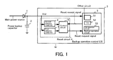
- Fig. 1 is a structural view of a reset circuit according to a first embodiment of the present invention.
- the reference numeral "1" denotes a diode
- "2" denotes a power backup capacitor
- "3" denotes a backup operation control LSI (Large-scale integration).
- the LSI includes a reset circuit 4 and a backup operation circuit 5.
- a power supply line from a main power source is connected to the reset circuit 4 and the backup operation circuit 5 via the diode 1.
- a power backup capacitor 2 Connected between the diode 1 and the LSI 3 is a power backup capacitor 2 for supplying a backup power to the LSI 3.
- the diode 1 is arranged to prevent electric charges stored in the power backup capacitor 2 from flowing back to the main power source when the power supply from the main power source is interrupted.
- the reset circuit 4 includes a first detector 7, a second detector 8, and a control circuit (controller) 9.
- the first detector 7 and the second detector 8 are each arranged to detect a voltage of the backup capacitor 2, and the detection voltage of each of the first and second detectors 7 and 8 can be set arbitrarily, respectively.
- a first voltage V1 and a second voltage V2 will be detected by the first detector 7 and the second detector 8, respectively, for the reset operation of the LSI 3.
- a normal voltage applied to the backup operation control LSI 3 when the main power supply is active is defied as "V0,” and the operation minimum voltage of the LSI 3 is defined as "Vmin,” and the first voltage V1 and the second voltage V2 will be set so as to meet the condition of VO>Vl>V2>Vmin, as shown in Fig. 2 .
- the voltage of the backup capacitor 2 When the main power supply is active, the voltage of the backup capacitor 2 is in a fully-charged state and maintains the voltage V0. Thereafter, when the main power supply is interrupted for some reasons, the backup capacitor 2 starts to supply the voltage to the LSI 3. As the backup capacitor 2 is discharged, the voltage of the backup capacitor 2 gradually decreases, becomes lower than V1, and then becomes lower than V2 as shown in Fig. 2 .
- the control circuit 9 After the voltage of the backup capacitor 2 became lower than V2, when the main power supply is resumed, the voltage of the power supply line starts to rise, becomes higher than V2, and then becomes higher than V1. At this period, the control circuit 9 outputs a reset request signal to the backup operation circuit 5.
- the first detector 7 initially detects the first voltage V1 during the drop of the voltage. In the initial state, however, the control circuit 9 prohibits outputting the reset request signal to the backup operation circuit 5 based on the detection result of the first detector 7.
- the control circuit 9 now allows outputting a reset request signal based on the detection result of the first detector 7.
- the controller 9 is configured to output the reset request signal when the voltage of the backup capacitor 2 once became lower than V2, and then became higher than V1.
- control circuit 9 can be configured such that, when the second detector 8 detects the second voltage 8, the control circuit 9 makes the first detector 7 detectable, so that the output of the first detector 7 can be used as a reset request signal as it is. In this case, the consumption current of the first detector 7 can be reduced by detecting the first voltage V1 only when needed.
- a reset signal is generated upon receipt of the reset request signal.
- the backup operation control LSI 3 When the backup operation control LSI 3 is reset, the backup operation circuit 5 generates a reset receipt signal and outputs it to the control circuit 9.
- the control circuit 9 which received the reset receipt signal makes the reset request signal inactive to terminate the reset request. With this operation, the backup operation control LSI 3 changes from the reset state to the normal operation state.
- the backup operation control LSI 3 in the backup operation control LSI 3, it can be configured to use a timer 52 embedded in the backup operation circuit 5 to set a reset period.
- the other circuit 51 can include a capacitor and a resistor to secure the stable secure reset period by the CR time constant of the capacitor and the resistor.
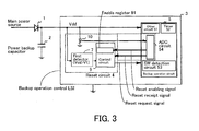
- Fig. 3 shows a second embodiment of the present invention.
- an ADC circuit (A/D converter circuit) 54 embedded in the backup operation circuit 5 is used as the second detector 8 shown in the first embodiment.
- the other structure is the same as that of the first embodiment, and therefore the cumulative explanation will be omitted by allotting the same reference numeral to the corresponding portion.
- the second detector 8 can be eliminated, which results in a reduced circuit size.
- one end of a resistor 10 is connected to the power supply line and the other end is grounded.
- a voltage obtained by dividing the power supply voltage Vdd with the resistor 10 is applied to the ADC circuit 54.
- the ADC circuit 54 can assume the power supply voltage Vdd depending on the magnitude of the voltage obtained by dividing the power supply voltage Vdd. This enables to detect whether or not the power supply voltage Vdd becomes lower than V2.
- the ADC circuit When the ADC circuit detects that the power supply voltage Vdd became lower than V2, the ADC circuit 54 outputs a reset enabling signal to the control circuit 9.
- This control circuit 9 is equipped with an enable register 91. Receiving the reset enabling signal, the control circuit 9 sets a permission flag which permits outputting a reset request signal in the enable register 91. When the main power supply is resumed and the power supply voltage gradually increases and becomes higher than V1 in a state in which the permission flag is set, the control circuit 9 can output a reset request signal.
- a reset signal is generated upon receipt of the reset request signal.
- the backup operation control LSI 3 When the backup operation control LSI 3 is reset, the backup operation circuit 5 generates a reset receipt signal and outputs it to the control circuit 9.
- the control circuit 9 which received the reset receipt signal makes the reset request signal inactive to terminate the reset request. With this, the backup operation control LSI 3 changes from the reset state to the normal operation state.
- the enable register 91 When the entire backup operation control LSI 3 is reset, the enable register 91 is initialized. This puts the flag down.
- the ADC circuit 54 is used in place of the second detector 8 of the first embodiment.
- Such ADC circuit 54 is high in general versatility and often embedded in an LSI for another purposes, and therefore can be effectively used.
- the term "preferably” is non-exclusive and means “preferably, but not limited to.”
- means-plus-function or step-plus-function limitations will only be employed where for a specific claim limitation all of the following conditions are present in that limitation: a) "means for” or “step for” is expressly recited; b) a corresponding function is expressly recited; and c) structure, material or acts that support that structure are not recited.
- the terminology "present invention” or “invention” is meant as a non-specific, general reference and may be used as a reference to one or more aspect within the present disclosure.
Landscapes
- Engineering & Computer Science (AREA)
- Theoretical Computer Science (AREA)
- Physics & Mathematics (AREA)
- General Engineering & Computer Science (AREA)
- General Physics & Mathematics (AREA)
- Electronic Switches (AREA)
Abstract
Description
- This application claims priority under 35 U.S.C. §119 to Japanese Patent Application No.
2009-224993 filed on September 29, 2009 - Some preferred embodiments of the present invention relate to a reset circuit for an electronic circuit equipped with a power backup capacitor.
- The following description sets forth the inventor's knowledge of related art and problems therein and should not be construed as an admission of knowledge in the prior art.
- In recent years, an electronic circuit, such as, e.g., an LSI circuit (hereinafter referred to as "electronic circuit",) mounting a power backup capacitor has been increasing. In such an electronic circuit, even if the power supply is interrupted due to, e.g., electric power failure, the electronic circuit can be continuously operated for a certain period of time using electric charges stored in the power backup capacitor. With this power backup capacitor, if the power failure continues only for a short period of time, for example, the data will not be cleared due to the power interruption. More specifically, in an electronic device having a timer recording function, the risk of occurrence of such inconvenience that the scheduled timer recording cannot be performed due to the power interruption can be reduced as low as possible.
- Electric charges stored in a power backup capacitor will reduce with time, and therefore it is required to reset the electronic circuit before the backup voltage becomes lower than the operation lower limit voltage of the circuit to prevent a runaway thereof.
- During the backup operation using the electric charges stored in the power backup capacitor, a predetermined voltage is generally used as a low reset voltage at which the circuit is reset when the backup voltage becomes lower than the predetermined voltage. When the power supply is resumed and then the backup voltage becomes higher than the reset voltage, the reset is terminated to resume the operation.
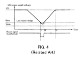
- In a normal low voltage reset circuit, as shown in
Fig. 4 , when the voltage of the power backup capacitor becomes lower than a predetermined low reset voltage, a reset request signal is outputted, and when the voltage of the power backup capacitor becomes higher than the predetermined low reset voltage, the reset request signal is released. The reset state will be maintained when the voltage of the power backup capacitor is kept lower than the predetermined low reset voltage. - According to the aforementioned prior art, however, during the process in which the voltage of the power backup capacitor raises after resuming of the power supply, there is a risk that a malfunction occurs during the voltage fluctuates before restoring to the normal operation voltage after exceeding the predetermined reset voltage.
- More specifically, for example, when power supply from the main power source is interrupted for some reasons, the electronic circuit enters into a backup state in which the circuit is operated by the electric charges stored in the power backup capacitor. The electric charges of the power backup capacitor gradually decrease with time, which in turn causes dropping of the voltage of the power backup capacitor. When the voltage reaches a predetermined voltage, the low voltage reset circuit resets the electronic circuit to prevent the possible malfunction. In order to secure the time from the interruption of the main power supply to the reset of the electronic circuit by detecting the low reset voltage as long as possible, it is required to approach the low reset voltage to the operation lower limit voltage Vmin of the LSI as close as possible.
- However, in cases where the low reset voltage is lowered too much, when the power supply is resumed and then the power supply voltage Vdd raises slightly, the reset state will be released. In this case, since the reset release timing is too early, the operation will be resumed at unstable voltages not sufficiently high. This may cause malfunction of the electronic circuit. To prevent such malfunction, if the low reset voltage is raised, the backup operation time becomes shorter.
- Even in cases where a reset voltage can be set using a microcomputer in a programmable manner, it is hard to find the most suitable low reset voltage value.
- Furthermore, in cases where a width of a conventional reset signal is increased using a counter, it is difficult to assuredly prevent the operation at unstable voltages while securing a sufficient time of the backup operation.
- The description herein of advantages and disadvantages of various features, embodiments, methods, and apparatus disclosed in other publications is in no way intended to limit the present invention. For example, certain features of the preferred embodiments of the invention may be capable of overcoming certain disadvantages and/or providing certain advantages, such as, e.g., disadvantages and/or advantages discussed herein, while retaining some or all of the features, embodiments, methods, and apparatus disclosed therein.
- The preferred embodiments of the present invention have been developed in view of the above-mentioned and/or other problems in the related art. The preferred embodiments of the present invention can significantly improve upon existing methods and/or apparatuses.
- Among other potential advantages, some embodiments can provide a reset circuit capable of minimizing a risk of malfunction of an electronic circuit when a power supply is resumed from a backup state.
- According to a first aspect of the present invention, among other potential advantages, some embodiments can provide a reset circuit including
- a first detector arranged to detect a predetermined first voltage of a power source;
- a second detector arranged to detect a predetermined second voltage of the power source, the second voltage being lower than the first voltage; and
- a controller arranged to control an output of a reset request signal based on detection results of the first detector and the second detector;
- In some examples, it can be configured such that the controller makes the first detector detectable after the second detector detected that a voltage of the backup capacitor became below the second voltage and makes an output from the first detector into the reset request signal.
- In some examples, it can be configured such that the controller is configured to receive a reset receipt signal and initialize the reset request signal to prohibit the reset request.
- In some examples, it can be configured such that the second detector is constituted by an ADC circuit,
wherein the controller includes a register, and
wherein the ADC circuit is configured to output a reset enabling signal to set a permission flag in the register to permit changing of the reset request signal when the permission flag is set. - According to a second aspect of the present invention, some preferred embodiments provide a reset circuit for an electronic circuit equipped with a power backup capacitor. The reset circuit includes a first detector arranged to detect a predetermined first voltage of the backup capacitor, a second detector arranged to detect a predetermined second voltage of the backup capacitor, the second voltage being lower than the first voltage, and a controller arranged to control an output of a reset request signal based on detection results of the first detector and the second detector. The controller is configured to output the reset request signal when the first detector detects the first voltage after the second detector detected the second voltage.
- According to a third aspect of the present invention, some preferred embodiments provide an electronic circuit equipped with a backup operation circuit, a reset circuit, and a power backup capacitor,
the reset circuit comprising: - a first detector arranged to detect a predetermined first voltage of the backup capacitor;
- a second detector arranged to detect a predetermined second voltage of the backup capacitor, the second voltage being lower than the first voltage; and
- a reset controller arranged to control an output of a reset request signal based on detection results of the first detector and the second detector,
- The above and/or other aspects, features and/or advantages of various embodiments will be further appreciated in view of the following description in conjunction with the accompanying figures. Various embodiments can include and/or exclude different aspects, features and/or advantages where applicable. In addition, various embodiments can combine one or more aspect or feature of other embodiments where applicable. The descriptions of aspects, features and/or advantages of particular embodiments should not be construed as limiting other embodiments or the claims.
- The preferred embodiments of the present invention are shown by way of example, and not limitation, in the accompanying figures, in which:
-
Fig. 1 is a schematic structural view showing a reset circuit according to a first embodiment of the present invention; -
Fig. 2 is a timing chart of an operation of the reset circuit of the first embodiment shown inFig. 1 ; -
Fig. 3 is a schematic structural view showing a reset circuit according to a second embodiment of the present invention; and -
Fig. 4 is a timing chart of an operation of a conventional reset circuit. - In the following paragraphs, some preferred embodiments of the present invention will be described by way of example and not limitation. It should be understood based on this disclosure that various other modifications can be made by those in the art based on these illustrated embodiments.
- Hereinafter, some preferable embodiments of the present invention will be explained with reference to the attached drawings. In the following explanation, although the reset circuit applied to a backup operation control LSI will be explained, it should be understood that the present invention can be applied to various electronic circuits.
-
Fig. 1 is a structural view of a reset circuit according to a first embodiment of the present invention. InFig. 1 , the reference numeral "1" denotes a diode, "2" denotes a power backup capacitor, and "3" denotes a backup operation control LSI (Large-scale integration). The LSI includes areset circuit 4 and abackup operation circuit 5. - A power supply line from a main power source is connected to the
reset circuit 4 and thebackup operation circuit 5 via the diode 1. Connected between the diode 1 and the LSI 3 is apower backup capacitor 2 for supplying a backup power to the LSI 3. The diode 1 is arranged to prevent electric charges stored in thepower backup capacitor 2 from flowing back to the main power source when the power supply from the main power source is interrupted. - The
reset circuit 4 includes afirst detector 7, asecond detector 8, and a control circuit (controller) 9. Thefirst detector 7 and thesecond detector 8 are each arranged to detect a voltage of thebackup capacitor 2, and the detection voltage of each of the first andsecond detectors - In this embodiment, two predetermined voltages, i.e., a first voltage V1 and a second voltage V2 will be detected by the
first detector 7 and thesecond detector 8, respectively, for the reset operation of the LSI 3. - In this embodiment, a normal voltage applied to the backup operation control LSI 3 when the main power supply is active is defied as "V0," and the operation minimum voltage of the LSI 3 is defined as "Vmin," and the first voltage V1 and the second voltage V2 will be set so as to meet the condition of VO>Vl>V2>Vmin, as shown in
Fig. 2 . - The operation of the
reset circuit 4 from the start of the power backup due to an interruption of the main power supply to the termination of the power backup due to the resuming of the main power supply will be explained with reference toFig. 2 . - When the main power supply is active, the voltage of the
backup capacitor 2 is in a fully-charged state and maintains the voltage V0. Thereafter, when the main power supply is interrupted for some reasons, thebackup capacitor 2 starts to supply the voltage to the LSI 3. As thebackup capacitor 2 is discharged, the voltage of thebackup capacitor 2 gradually decreases, becomes lower than V1, and then becomes lower than V2 as shown inFig. 2 . - After the voltage of the
backup capacitor 2 became lower than V2, when the main power supply is resumed, the voltage of the power supply line starts to rise, becomes higher than V2, and then becomes higher than V1. At this period, thecontrol circuit 9 outputs a reset request signal to thebackup operation circuit 5. - During this operation, the
first detector 7 initially detects the first voltage V1 during the drop of the voltage. In the initial state, however, thecontrol circuit 9 prohibits outputting the reset request signal to thebackup operation circuit 5 based on the detection result of thefirst detector 7. When thesecond detector 8 detected that the voltage of thebackup capacitor 2 became lower than V2 and then thefirst detector 7 detects that the voltage of thebackup capacitor 2 becomes higher than V1, thecontrol circuit 9 now allows outputting a reset request signal based on the detection result of thefirst detector 7. In other words, thecontroller 9 is configured to output the reset request signal when the voltage of thebackup capacitor 2 once became lower than V2, and then became higher than V1. - Alternatively, the
control circuit 9 can be configured such that, when thesecond detector 8 detects thesecond voltage 8, thecontrol circuit 9 makes thefirst detector 7 detectable, so that the output of thefirst detector 7 can be used as a reset request signal as it is. In this case, the consumption current of thefirst detector 7 can be reduced by detecting the first voltage V1 only when needed. - In the
backup operation circuit 5 which received the reset request signal outputted from thecontrol circuit 9, a reset signal is generated upon receipt of the reset request signal. When the backup operation control LSI 3 is reset, thebackup operation circuit 5 generates a reset receipt signal and outputs it to thecontrol circuit 9. Thecontrol circuit 9 which received the reset receipt signal makes the reset request signal inactive to terminate the reset request. With this operation, the backup operation control LSI 3 changes from the reset state to the normal operation state. - For the purpose of more stably resetting the backup operation control LSI 3, in the backup operation control LSI 3, it can be configured to use a
timer 52 embedded in thebackup operation circuit 5 to set a reset period. In cases where no timer is embedded in thebackup operation circuit 5, theother circuit 51 can include a capacitor and a resistor to secure the stable secure reset period by the CR time constant of the capacitor and the resistor. -
Fig. 3 shows a second embodiment of the present invention. In this embodiment, as thesecond detector 8 shown in the first embodiment, an ADC circuit (A/D converter circuit) 54 embedded in thebackup operation circuit 5 is used. The other structure is the same as that of the first embodiment, and therefore the cumulative explanation will be omitted by allotting the same reference numeral to the corresponding portion. - By using the
ADC circuit 54 in place of thesecond detector 8 of the first embodiment, thesecond detector 8 can be eliminated, which results in a reduced circuit size. In this embodiment, one end of aresistor 10 is connected to the power supply line and the other end is grounded. A voltage obtained by dividing the power supply voltage Vdd with theresistor 10 is applied to theADC circuit 54. TheADC circuit 54 can assume the power supply voltage Vdd depending on the magnitude of the voltage obtained by dividing the power supply voltage Vdd. This enables to detect whether or not the power supply voltage Vdd becomes lower than V2. - When the ADC circuit detects that the power supply voltage Vdd became lower than V2, the
ADC circuit 54 outputs a reset enabling signal to thecontrol circuit 9. Thiscontrol circuit 9 is equipped with an enableregister 91. Receiving the reset enabling signal, thecontrol circuit 9 sets a permission flag which permits outputting a reset request signal in the enableregister 91. When the main power supply is resumed and the power supply voltage gradually increases and becomes higher than V1 in a state in which the permission flag is set, thecontrol circuit 9 can output a reset request signal. - In the
backup operation circuit 5 which received the reset request signal outputted from thecontrol circuit 9, a reset signal is generated upon receipt of the reset request signal. When the backup operation control LSI 3 is reset, thebackup operation circuit 5 generates a reset receipt signal and outputs it to thecontrol circuit 9. Thecontrol circuit 9 which received the reset receipt signal makes the reset request signal inactive to terminate the reset request. With this, the backup operation control LSI 3 changes from the reset state to the normal operation state. When the entire backup operation control LSI 3 is reset, the enableregister 91 is initialized. This puts the flag down. - In this second embodiment, the
ADC circuit 54 is used in place of thesecond detector 8 of the first embodiment.Such ADC circuit 54 is high in general versatility and often embedded in an LSI for another purposes, and therefore can be effectively used. - While the present invention may be embodied in many different forms, a number of illustrative embodiments are described herein with the understanding that the present disclosure is to be considered as providing examples of the principles of the invention and such examples are not intended to limit the invention to preferred embodiments described herein and/or illustrated herein.
- While illustrative embodiments of the invention have been described herein, the present invention is not limited to the various preferred embodiments described herein, but includes any and all embodiments having equivalent elements, modifications, omissions, combinations (e.g., of aspects across various embodiments), adaptations and/or alterations as would be appreciated by those in the art based on the present disclosure. The limitations in the claims are to be interpreted broadly based on the language employed in the claims and not limited to examples described in the present specification or during the prosecution of the application, which examples are to be construed as non-exclusive. For example, in the present disclosure, the term "preferably" is non-exclusive and means "preferably, but not limited to." In this disclosure and during the prosecution of this application, means-plus-function or step-plus-function limitations will only be employed where for a specific claim limitation all of the following conditions are present in that limitation: a) "means for" or "step for" is expressly recited; b) a corresponding function is expressly recited; and c) structure, material or acts that support that structure are not recited. In this disclosure and during the prosecution of this application, the terminology "present invention" or "invention" is meant as a non-specific, general reference and may be used as a reference to one or more aspect within the present disclosure. The language present invention or invention should not be improperly interpreted as an identification of criticality, should not be improperly interpreted as applying across all aspects or embodiments (i.e., it should be understood that the present invention has a number of aspects and embodiments), and should not be improperly interpreted as limiting the scope of the application or claims. In this disclosure and during the prosecution of this application, the terminology "embodiment" can be used to describe any aspect, feature, process or step, any combination thereof, and/or any portion thereof, etc. In some examples, various embodiments may include overlapping features. In this disclosure and during the prosecution of this case, the following abbreviated terminology may be employed: "e.g." which means "for example;" and "NB" which means "note well:'
Claims (12)
- A reset circuit comprising:a first detector arranged to detect a predetermined first voltage of a power source;a second detector arranged to detect a predetermined second voltage of the power source, the second voltage being lower than the first voltage; anda controller arranged to control an output of a reset request signal based on detection results of the first detector and the second detector,wherein the controller is configured to output the reset request signal when the first detector detects the first voltage after the second detector detected the second voltage.
- The reset circuit as recited in claim 1, wherein the controller makes the first detector detectable after the second detector detected that a voltage of the backup capacitor became below the second voltage and makes an output from the first detector into the reset request signal.
- The reset circuit as recited in claim 2, wherein the controller is configured to receive a reset receipt signal and initialize the reset request signal to prohibit the reset request.
- The reset circuit as recited in claim 1,
wherein the second detector is constituted by an ADC circuit,
wherein the controller includes a register, and
wherein the ADC circuit is configured to output a reset enabling signal to set a permission flag in the register to permit changing of the reset request signal when the permission flag is set. - A reset circuit for an electronic circuit equipped with a power backup capacitor,
the reset circuit comprising:a first detector arranged to detect a predetermined first voltage of the backup capacitor;a second detector arranged to detect a predetermined second voltage of the backup capacitor, the second voltage being lower than the first voltage; anda controller arranged to control an output of a reset request signal based on detection results of the first detector and the second detector,wherein the controller is configured to output the reset request signal when the first detector detects the first voltage after the second detector detected the second voltage. - The reset circuit as recited in claim 5, wherein the controller makes the first detector detectable after the second detector detected that a voltage of the backup capacitor became below the second voltage and makes an output from the first detector into the reset request signal.
- The reset circuit as recited in claim 6, wherein the controller is configured to receive a reset receipt signal and initialize the reset request signal to prohibit the reset request.
- The reset circuit as recited in claim 5,
wherein the second detector is constituted by an ADC circuit,
wherein the controller includes a register, and
wherein the ADC circuit is configured to output a reset enabling signal to set a permission flag in the register to permit changing of the reset request signal when the permission flag is set. - An electronic circuit equipped with a backup operation circuit, a reset circuit, and a power backup capacitor,
the reset circuit comprising:a first detector arranged to detect a predetermined first voltage of the backup capacitor;a second detector arranged to detect a predetermined second voltage of the backup capacitor, the second voltage being lower than the first voltage; anda reset controller arranged to control an output of a reset request signal based on detection results of the first detector and the second detector,wherein the controller is configured to output the reset request signal to the backup operation circuit when the first detector detects the first voltage after the second detector detected the second voltage. - The reset circuit as recited in claim 9, wherein the controller makes the first detector detectable after the second detector detected that a voltage of the backup capacitor became below the second voltage and makes an output from the first detector into the reset request signal.
- The reset circuit as recited in claim 10, wherein the controller is configured to receive a reset receipt signal and initialize the reset request signal to prohibit the reset request.
- The reset circuit as recited in claim 9,
wherein the second detector is constituted by an ADC circuit,
wherein the controller includes a register, and
wherein the ADC circuit is configured to output a reset enabling signal to set a permission flag in the register to permit changing of the reset request signal when the permission flag is set.
Applications Claiming Priority (1)
| Application Number | Priority Date | Filing Date | Title |
|---|---|---|---|
| JP2009224993A JP5308298B2 (en) | 2009-09-29 | 2009-09-29 | Reset circuit |
Publications (2)
| Publication Number | Publication Date |
|---|---|
| EP2306266A2 true EP2306266A2 (en) | 2011-04-06 |
| EP2306266A3 EP2306266A3 (en) | 2012-10-17 |
Family
ID=43017132
Family Applications (1)
| Application Number | Title | Priority Date | Filing Date |
|---|---|---|---|
| EP10182194A Withdrawn EP2306266A3 (en) | 2009-09-29 | 2010-09-29 | Reset circuit |
Country Status (5)
| Country | Link |
|---|---|
| US (2) | US8653864B2 (en) |
| EP (1) | EP2306266A3 (en) |
| JP (1) | JP5308298B2 (en) |
| KR (1) | KR101148240B1 (en) |
| CN (1) | CN102035517B (en) |
Cited By (2)
| Publication number | Priority date | Publication date | Assignee | Title |
|---|---|---|---|---|
| EP2566294A1 (en) * | 2011-08-31 | 2013-03-06 | Koninklijke Philips Electronics N.V. | Appliance control device |
| EP2966743A4 (en) * | 2013-03-05 | 2016-10-19 | Huizhou Kimree Technology Co Ltd Shenzhen Branch | Protection device and method for preventing power source voltage of microcontroller from dropping in electronic cigarette |
Families Citing this family (3)
| Publication number | Priority date | Publication date | Assignee | Title |
|---|---|---|---|---|
| JP5308298B2 (en) * | 2009-09-29 | 2013-10-09 | セミコンダクター・コンポーネンツ・インダストリーズ・リミテッド・ライアビリティ・カンパニー | Reset circuit |
| JP4868051B2 (en) * | 2009-10-23 | 2012-02-01 | ミツミ電機株式会社 | Operation input device and control method thereof |
| FR3072221B1 (en) * | 2017-10-09 | 2021-03-26 | Continental Automotive France | POWER SUPPLY DEVICE FOR AN ELECTRONIC COMPUTER |
Family Cites Families (16)
| Publication number | Priority date | Publication date | Assignee | Title |
|---|---|---|---|---|
| JPS5923822U (en) * | 1982-07-31 | 1984-02-14 | 日本電気ホームエレクトロニクス株式会社 | Power outage compensation reset circuit |
| JPS61155928U (en) * | 1985-03-20 | 1986-09-27 | ||
| JPS61240303A (en) * | 1985-04-17 | 1986-10-25 | Toshiba Corp | Washing machine |
| JP3113516B2 (en) * | 1994-09-26 | 2000-12-04 | 三洋電機株式会社 | Reset pulse generation circuit |
| JP3802239B2 (en) * | 1998-08-17 | 2006-07-26 | 株式会社東芝 | Semiconductor integrated circuit |
| US6025981A (en) * | 1998-11-04 | 2000-02-15 | Mosel Vitelic Inc. | Flexible voltage transient detector circuit |
| JP2001285046A (en) * | 2000-03-31 | 2001-10-12 | Hitachi Ltd | Reset signal generation circuit and semiconductor integrated circuit |
| US20030140261A1 (en) * | 2002-01-24 | 2003-07-24 | Minoru Takasaki | Control apparatus |
| KR20040102736A (en) * | 2003-05-29 | 2004-12-08 | 매그나칩 반도체 유한회사 | Reset signal generator can discriminate power fail reset and power on reset |
| JP2005086108A (en) * | 2003-09-10 | 2005-03-31 | Renesas Technology Corp | Semiconductor integrated circuit |
| JP2007157199A (en) * | 2005-12-01 | 2007-06-21 | Matsushita Electric Ind Co Ltd | Semiconductor device |
| JP5111791B2 (en) * | 2006-06-20 | 2013-01-09 | オンセミコンダクター・トレーディング・リミテッド | Low voltage detection reset circuit |
| US7567098B2 (en) * | 2006-08-31 | 2009-07-28 | Atmel Corporation | Multi-threshold reset circuit |
| JP2009134564A (en) * | 2007-11-30 | 2009-06-18 | Daikin Ind Ltd | Operation control device for electrical equipment |
| KR101022673B1 (en) * | 2009-06-16 | 2011-03-22 | 주식회사 하이닉스반도체 | Power-Up Circuit of Semiconductor Memory Device |
| JP5308298B2 (en) * | 2009-09-29 | 2013-10-09 | セミコンダクター・コンポーネンツ・インダストリーズ・リミテッド・ライアビリティ・カンパニー | Reset circuit |
-
2009
- 2009-09-29 JP JP2009224993A patent/JP5308298B2/en active Active
-
2010
- 2010-08-24 KR KR1020100081954A patent/KR101148240B1/en not_active Expired - Fee Related
- 2010-09-28 CN CN2010102970659A patent/CN102035517B/en not_active Expired - Fee Related
- 2010-09-29 EP EP10182194A patent/EP2306266A3/en not_active Withdrawn
- 2010-09-29 US US12/893,755 patent/US8653864B2/en active Active
-
2014
- 2014-02-14 US US14/181,013 patent/US9209796B2/en active Active
Non-Patent Citations (1)
| Title |
|---|
| None |
Cited By (3)
| Publication number | Priority date | Publication date | Assignee | Title |
|---|---|---|---|---|
| EP2566294A1 (en) * | 2011-08-31 | 2013-03-06 | Koninklijke Philips Electronics N.V. | Appliance control device |
| WO2013030719A1 (en) * | 2011-08-31 | 2013-03-07 | Koninklijke Philips Electronics N.V. | Appliance control device |
| EP2966743A4 (en) * | 2013-03-05 | 2016-10-19 | Huizhou Kimree Technology Co Ltd Shenzhen Branch | Protection device and method for preventing power source voltage of microcontroller from dropping in electronic cigarette |
Also Published As
| Publication number | Publication date |
|---|---|
| EP2306266A3 (en) | 2012-10-17 |
| US20140232437A1 (en) | 2014-08-21 |
| KR101148240B1 (en) | 2012-05-21 |
| US20110074473A1 (en) | 2011-03-31 |
| US20150381164A9 (en) | 2015-12-31 |
| CN102035517A (en) | 2011-04-27 |
| KR20110035857A (en) | 2011-04-06 |
| CN102035517B (en) | 2013-09-11 |
| JP2011077673A (en) | 2011-04-14 |
| JP5308298B2 (en) | 2013-10-09 |
| US9209796B2 (en) | 2015-12-08 |
| US8653864B2 (en) | 2014-02-18 |
Similar Documents
| Publication | Publication Date | Title |
|---|---|---|
| US9209796B2 (en) | Method for operating a backup circuit and circuit therefor | |
| US9430008B2 (en) | Apparatus and method for optimizing use of NVDC chargers | |
| US9841805B2 (en) | Power management circuit and electronic device employing the same | |
| US8629713B2 (en) | System and method for controlling bypass of a voltage regulator | |
| US8179111B2 (en) | Methods, systems, and devices for power-on sequence for a circuit | |
| CN106486154B (en) | Memory control circuit for controlling memory device and control method thereof | |
| US20100090730A1 (en) | Circuit and method of adjusting system clock in low voltage detection, and low voltage reset circuit | |
| US20090027991A1 (en) | Information processing apparatus, memory unit erroneous write preventing method, and information processing system | |
| JP4322810B2 (en) | Integrated circuit and low voltage detection system | |
| US9436248B2 (en) | Data processing system with protocol determination circuitry | |
| US20150362982A1 (en) | Server system and cluster system using the same | |
| US10951228B2 (en) | Semiconductor apparatus | |
| US9501113B2 (en) | Voltage detection system and controlling method of the same | |
| US7882392B2 (en) | Electronic device and method of controlling electronic device | |
| US8578199B2 (en) | Resetting real time clock upon reference clock interruption | |
| EP2860634A1 (en) | Electronic device | |
| US6903583B1 (en) | Power supply shutdown control | |
| US11294445B2 (en) | Information processing apparatus and method of controlling information processing apparatus | |
| US7243220B2 (en) | Networking apparatus and method capable of wake-on-LAN after improper shutdown | |
| US20110242718A1 (en) | Protection circuit for central processing unit | |
| US12424933B2 (en) | Power consumption control of an electronic system and apparatus for controlling the power consumption | |
| US20130051086A1 (en) | Control circuits and control methods for over voltage protection in power suppliers | |
| US12625536B2 (en) | Circuit to protect against multi-rail voltage glitching attacks | |
| US10079487B2 (en) | Clamp circuit for electrical overstress and electrostatic discharge | |
| EP2833240A2 (en) | Electronic device |
Legal Events
| Date | Code | Title | Description |
|---|---|---|---|
| PUAI | Public reference made under article 153(3) epc to a published international application that has entered the european phase |
Free format text: ORIGINAL CODE: 0009012 |
|
| AK | Designated contracting states |
Kind code of ref document: A2 Designated state(s): AL AT BE BG CH CY CZ DE DK EE ES FI FR GB GR HR HU IE IS IT LI LT LU LV MC MK MT NL NO PL PT RO SE SI SK SM TR |
|
| AX | Request for extension of the european patent |
Extension state: BA ME RS |
|
| PUAL | Search report despatched |
Free format text: ORIGINAL CODE: 0009013 |
|
| AK | Designated contracting states |
Kind code of ref document: A3 Designated state(s): AL AT BE BG CH CY CZ DE DK EE ES FI FR GB GR HR HU IE IS IT LI LT LU LV MC MK MT NL NO PL PT RO SE SI SK SM TR |
|
| AX | Request for extension of the european patent |
Extension state: BA ME RS |
|
| RIC1 | Information provided on ipc code assigned before grant |
Ipc: G06F 1/24 20060101AFI20120913BHEP |
|
| 17P | Request for examination filed |
Effective date: 20130417 |
|
| 17Q | First examination report despatched |
Effective date: 20130606 |
|
| STAA | Information on the status of an ep patent application or granted ep patent |
Free format text: STATUS: THE APPLICATION IS DEEMED TO BE WITHDRAWN |
|
| 18D | Application deemed to be withdrawn |
Effective date: 20131217 |