EP2302776A1 - Voltage detecting device for half bridge circuit - Google Patents
Voltage detecting device for half bridge circuit Download PDFInfo
- Publication number
- EP2302776A1 EP2302776A1 EP10179241A EP10179241A EP2302776A1 EP 2302776 A1 EP2302776 A1 EP 2302776A1 EP 10179241 A EP10179241 A EP 10179241A EP 10179241 A EP10179241 A EP 10179241A EP 2302776 A1 EP2302776 A1 EP 2302776A1
- Authority
- EP
- European Patent Office
- Prior art keywords
- voltage
- transistors
- value
- terminal
- capacitor
- Prior art date
- Legal status (The legal status is an assumption and is not a legal conclusion. Google has not performed a legal analysis and makes no representation as to the accuracy of the status listed.)
- Granted
Links
Images
Classifications
-
- H—ELECTRICITY
- H02—GENERATION; CONVERSION OR DISTRIBUTION OF ELECTRIC POWER
- H02M—APPARATUS FOR CONVERSION BETWEEN AC AND AC, BETWEEN AC AND DC, OR BETWEEN DC AND DC, AND FOR USE WITH MAINS OR SIMILAR POWER SUPPLY SYSTEMS; CONVERSION OF DC OR AC INPUT POWER INTO SURGE OUTPUT POWER; CONTROL OR REGULATION THEREOF
- H02M1/00—Details of apparatus for conversion
- H02M1/08—Circuits specially adapted for the generation of control voltages for semiconductor devices incorporated in static converters
- H02M1/083—Circuits specially adapted for the generation of control voltages for semiconductor devices incorporated in static converters for the ignition at the zero crossing of the voltage or the current
-
- H—ELECTRICITY
- H02—GENERATION; CONVERSION OR DISTRIBUTION OF ELECTRIC POWER
- H02M—APPARATUS FOR CONVERSION BETWEEN AC AND AC, BETWEEN AC AND DC, OR BETWEEN DC AND DC, AND FOR USE WITH MAINS OR SIMILAR POWER SUPPLY SYSTEMS; CONVERSION OF DC OR AC INPUT POWER INTO SURGE OUTPUT POWER; CONTROL OR REGULATION THEREOF
- H02M1/00—Details of apparatus for conversion
- H02M1/38—Means for preventing simultaneous conduction of switches
-
- H—ELECTRICITY
- H02—GENERATION; CONVERSION OR DISTRIBUTION OF ELECTRIC POWER
- H02M—APPARATUS FOR CONVERSION BETWEEN AC AND AC, BETWEEN AC AND DC, OR BETWEEN DC AND DC, AND FOR USE WITH MAINS OR SIMILAR POWER SUPPLY SYSTEMS; CONVERSION OF DC OR AC INPUT POWER INTO SURGE OUTPUT POWER; CONTROL OR REGULATION THEREOF
- H02M3/00—Conversion of DC power input into DC power output
- H02M3/22—Conversion of DC power input into DC power output with intermediate conversion into AC
- H02M3/24—Conversion of DC power input into DC power output with intermediate conversion into AC by static converters
- H02M3/28—Conversion of DC power input into DC power output with intermediate conversion into AC by static converters using discharge tubes with control electrode or semiconductor devices with control electrode to produce the intermediate AC
- H02M3/325—Conversion of DC power input into DC power output with intermediate conversion into AC by static converters using discharge tubes with control electrode or semiconductor devices with control electrode to produce the intermediate AC using devices of a triode or a transistor type requiring continuous application of a control signal
- H02M3/335—Conversion of DC power input into DC power output with intermediate conversion into AC by static converters using discharge tubes with control electrode or semiconductor devices with control electrode to produce the intermediate AC using devices of a triode or a transistor type requiring continuous application of a control signal using semiconductor devices only
- H02M3/33569—Conversion of DC power input into DC power output with intermediate conversion into AC by static converters using discharge tubes with control electrode or semiconductor devices with control electrode to produce the intermediate AC using devices of a triode or a transistor type requiring continuous application of a control signal using semiconductor devices only having several active switching elements
- H02M3/33571—Half-bridge at primary side of an isolation transformer
-
- H—ELECTRICITY
- H02—GENERATION; CONVERSION OR DISTRIBUTION OF ELECTRIC POWER
- H02M—APPARATUS FOR CONVERSION BETWEEN AC AND AC, BETWEEN AC AND DC, OR BETWEEN DC AND DC, AND FOR USE WITH MAINS OR SIMILAR POWER SUPPLY SYSTEMS; CONVERSION OF DC OR AC INPUT POWER INTO SURGE OUTPUT POWER; CONTROL OR REGULATION THEREOF
- H02M1/00—Details of apparatus for conversion
- H02M1/0048—Circuits or arrangements for reducing losses
- H02M1/0054—Transistor switching losses
- H02M1/0058—Transistor switching losses by employing soft switching techniques, i.e. commutation of transistors when applied voltage is zero or when current flow is zero
-
- H—ELECTRICITY
- H02—GENERATION; CONVERSION OR DISTRIBUTION OF ELECTRIC POWER
- H02M—APPARATUS FOR CONVERSION BETWEEN AC AND AC, BETWEEN AC AND DC, OR BETWEEN DC AND DC, AND FOR USE WITH MAINS OR SIMILAR POWER SUPPLY SYSTEMS; CONVERSION OF DC OR AC INPUT POWER INTO SURGE OUTPUT POWER; CONTROL OR REGULATION THEREOF
- H02M3/00—Conversion of DC power input into DC power output
- H02M3/01—Resonant DC/DC converters
-
- Y—GENERAL TAGGING OF NEW TECHNOLOGICAL DEVELOPMENTS; GENERAL TAGGING OF CROSS-SECTIONAL TECHNOLOGIES SPANNING OVER SEVERAL SECTIONS OF THE IPC; TECHNICAL SUBJECTS COVERED BY FORMER USPC CROSS-REFERENCE ART COLLECTIONS [XRACs] AND DIGESTS
- Y02—TECHNOLOGIES OR APPLICATIONS FOR MITIGATION OR ADAPTATION AGAINST CLIMATE CHANGE
- Y02B—CLIMATE CHANGE MITIGATION TECHNOLOGIES RELATED TO BUILDINGS, e.g. HOUSING, HOUSE APPLIANCES OR RELATED END-USER APPLICATIONS
- Y02B70/00—Technologies for an efficient end-user side electric power management and consumption
- Y02B70/10—Technologies improving the efficiency by using switched-mode power supplies [SMPS], i.e. efficient power electronics conversion e.g. power factor correction or reduction of losses in power supplies or efficient standby modes
Definitions
- the present invention relates to a detecting device for a midpoint voltage of a transistor half bridge circuit.
- the circuits with high voltage transistor half bridges are employed in various applications, such as motor control, ballast for fluorescent lamps and supply circuits.
- the half bridge circuits consist of a pair of stacked transistors placed between a high supply voltage Vin and the ground GND, as seen in figure 1 .
- the transistors Q1 and Q2 are power devices of MOSFET type and their common connection point, node "A", is the output connected to the load.
- Each transistor Q1 and Q2 has its driving driver DRV1 and DRV2 providing the convenient signals for switching them on or off.
- monitoring the center-point node, node A is convenient for determining when this switched from a high state to a low state or vice versa, such as, for example, the LLC series resonant circuit 1 in figure 1 .
- the transistors Q1 and Q2 are alternately switched on and off to make the current flow into the resonant load connected to node A.
- transistor Q1 When transistor Q1 is switched on, the voltage of node A is brought to the high potential, substantially the supply voltage, and so the current starts increasing in the resonant load.
- transistor Q1 is switched off, the current flowing into the resonant load causes the voltage of node A to decrease towards a low potential.
- the transistors Q1 and Q2 are assumed to switch at a frequency which is higher than the resonance frequency of the load circuit. After a certain idle time such to ensure that the voltage of node A has decreased to a low voltage which is typically 0 volts, i.e. the ground GND, the transistor Q2 is switched on.
- the idle time avoids both transistors Q1, Q2 from being simultaneously switched on, which would cause a short circuit between the high and low voltages; the idle time ensures that the transition of the voltage of node A, i.e. the voltage of the midpoint node, is already over before switching on the other transistor.
- the switching losses may be minimized thus ensuring that node A has finished the transition from the high voltage to the low voltage or vice versa before switching on the transistors.
- a detecting device for a midpoint voltage of a transistor half bridge circuit comprising first and second transistors, said half bridge being connected between a voltage supply and a reference voltage and being adapted to drive a load, said first and second transistors being driven so that said midpoint voltage undergoes transitions from a low voltage value to a high voltage value and vice versa
- said half bridge circuit comprising a bootstrap capacitor having one terminal connected to the midpoint node and the other terminal connected to a supply circuit of said bootstrap capacitor, characterized in that it comprises a further capacitor adapted to be connected between said other terminal of said bootstrap capacitor and circuit means adapted to form a low impedance node for the current signal circulating in said further capacitor during the transitions from the low value to the high value and from the high value to the low value of the midpoint voltage, detecting means adapted to detect said current signal circulating in said further capacitor and adapted to output at least a first signal indicating the transitions from the low value to the high value or
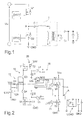
- Figure 2 shows a detecting device or circuit 10 for a midpoint voltage of a transistor half bridge circuit in accordance with the present invention.
- the figure shows a half bridge of MOS transistors M1 and M2 arranged in series between the supply voltage Vcc and the ground GND.
- the center-point node A i.e. the common terminal between the transistors M1 and M2, is connected to a load LOAD, preferably a resonant load, connected to the ground GND.
- the transistors M1 and M2 are driven by two drivers 11 and 21, respectively, having the input signals HVG and LVG, respectively.
- the drivers 11 and 21 are adapted to alternately switch on and off the transistors M1 and M2 so that when transistor M1 is on and transistor M2 is off, node A is at a high potential, substantially at the voltage Vcc, for example 400 Volts, whilst when transistor M2 is on and transistor M1 is off, node A is at a low potential, substantially at the ground voltage GND.
- transistor M1 When transistor M1 is switched off, the current flowing into the resonant load causes the voltage of node A to decrease towards a low potential LW.
- the transistors M1 and M2 are assumed to switch at a frequency which is higher than the resonance frequency of the load LOAD.
- Tm1 After a certain idle time Tm1, i.e. once the voltage of node A has been brought to a low voltage which is typically 0 volts, i.e. the ground GND, transistor M2 is switched on.
- the idle time Tm1 avoids both transistors M1, M2 from being simultaneously switched on, which would cause a short circuit between the high and low voltages; the idle time Tm1 ensures that the transition of the voltage of node A, i.e. the voltage of the midpoint node, is already over before switching on the other transistor M1.
- the current flowing into the resonant load causes the voltage of node A to increase towards a high potential HW.
- a certain idle time Tm2 i.e. once the voltage of node A has been brought to a high voltage which is typically the supply voltage Vcc, transistor M1 is switched on.
- the idle time Tm2 avoids both transistors M1, M2 from being simultaneously switched on, which would cause a short circuit between the high and low voltages; the idle time Tm2 ensures that the transition of the voltage of node A, i.e. the voltage of the midpoint node, is already over before switching on the other transistor M2.
- Circuit 10 is adapted to detect the voltage variations in the center-point node A and provide logic signals at said variations, in particular it is adapted to detect the transitions from a low voltage value LW to a high voltage value HW and vice versa of the midpoint voltage Va.
- the half bridge circuit normally also comprises a bootstrap capacitor Cboot connected to the center-point node A and a specific supply circuit 15 of said bootstrap capacitor Cboot.
- the bootstrap capacitor allows the driving stage of the transistor M1 to be correctly supplied; in order to ensure a charge of the bootstrap capacitor Cboot in a very short time, circuit 15 should allow the supply thereof in a short time.
- Circuit 10 comprises a circuitry with a further capacitor connectable to the bootstrap capacitor Cboot and to circuit means 12, Cpump, Q3, Q4 which form a low impedance node for the current signal crossing said further capacitor during the transitions from the low value LW to the high value HW and from the high value HW to the low value LW of the midpoint voltage Va.
- the high voltage value HW substantially is the supply voltage Vcc whilst the low voltage value LW is a reference voltage, preferably the ground GND.
- Circuit 15 preferably comprises a LDMOS transistor M10 having a non-drivable terminal, e.g. the source terminal, connected to a voltage Vdd, e.g.
- the further capacitor is the inherent capacitor Cgd between the gate terminal and the drain terminal of the transistor M10.
- an internal charge pump 12 comprising a driving circuit 12A preferably controlled by the signal LVG, a pumping capacitor Cpump connected between the output of the driving circuit 12A and coupled to the gate terminal G of transistor M10 and a diode D1 having the anode connected to the supply voltage Vdd and the cathode coupled to the gate terminal G of the transistor M10.
- the pumping circuit 12 preferably comprises at least one inverter, connected between the supply voltage Vdd and the ground GND and having the output terminal connected to the capacitor Cpump; the output terminal being the common terminal of the two transistors of the inverter.
- Circuit 10 exploits the inherent gate-drain capacitor Cgd of the LDMOS transistor M10 to monitor the voltage variation on node A; the capacitor Cgd is usually in the range between 0.5 and 1 pF.
- the coupling between the gate terminal of transistor M10 and a terminal of the capacitor Cpump and the cathode of diode D1 is achieved by a resistor Rswitch.
- Circuit 10 comprises a circuitry 20 with a bipolar transistor Q3 of the npn type having the emitter terminal directly connected to the gate terminal G of transistor M10 and connected to a terminal of the resistor Rswitch, the base terminal connected to the other terminal of the resistor Rswitch and the collector terminal connected to a current mirror T1-T2, comprising the p-channel MOS transistors T1 and T2, connected to a current generator I1.
- Circuitry 20 also comprises a bipolar transistor Q4 of the pnp type having the emitter terminal directly connected to the gate terminal G of transistor M10 and connected to a terminal of the resistor Rswitch, the base terminal connected to the other terminal of the resistor Rswitch and the collector terminal connected to a current mirror T3-T4, comprising the n-channel MOS transistors T3 and T4, connected to a current generator 12.
- the transistors Q3 and Q4 could also consist of MOS transistors having the gate terminal connected to the gate terminal G of transistor M10 and connected to a terminal of the resistor Rswitch, the gate terminals both connected to the other terminal of the resistor Rswitch and the drain terminals connected to the current mirrors T1-T2 and T3-T4.
- a current Isink is injected into the gate terminal G of the transistor M10 by the capacitor Cgd. Said current crosses the resistor Rswitch and flows on the capacitor Cpump that, from the point of view of the current signal, is a low impedance point and causes a voltage drop on the resistor Rswitch; this causes the bipolar transistor Q4 to be switched on, which transistor Q4 tends to divert the current Isink towards the mirror T3-T4.
- the current Isink is compared to the reference current 12 from the current generator 12 and provides, through an inverter 13, a high logic output signal LH_comm when the current Isink is higher than current 12.
- a current Isource is picked up from the gate terminal G of transistor M10 by the capacitor Cgd. Said current crosses the resistor Rswitch and flows on the capacitor Cpump that, from the point of view of the current signal, is a low impedance point and causes the voltage to drop on the resistor Rswitch; this causes the bipolar transistor Q3 to be switched on, which transistor Q3 tends to divert the current Isource towards the mirror T1-T2.
- the current Isource is compared to the reference current I1 from the current generator I1 and provides, through a buffer 14, a high logic output signal HL_comm when the current Isource is higher than current I1.
- the signal currents Isink and Isource are proportional to the derivative of the voltage of the center-point node A. Indeed, as one of the two bipolar transistors Q3 or Q4 is switched on when the current is injected into or picked up from the gate node G of transistor M10, the impedance seen by the current from the gate node towards the ground is relatively low, i.e. the emitting resistor of the bipolar transistor.
- I sin k / source Cgd ⁇ dVboot dt
- the signal currents Isink and Isource are proportional to the derivative of the center-point voltage Va. Therefore, the logic signals LH_comm and HL_comm, which are active-high when the positive/negative derivative of the voltage Va exceeds a certain value determined by the reference currents I1 and 12, indicate when a transition of node A occurs.
- the activation sensitivity of the logic signals HL_comm and LH_comm may be set to the variations of the voltage Va. Instead, the value of the resistor Rswitch determines the minimum threshold of the signal current Isink and Isource which activates the sensing circuitry.
- the above-described circuit 10 may be integrated in the same chip containing the bootstrap and control circuitry, without employing additional external components and thus simplifying the final application circuit.
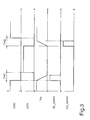
- Figure 3 shows the time charts of signals HVG and LVG, midpont voltage Va and signals HL_comm and LH_comm, and the idle time periods Tm1 and Tm2.
Landscapes
- Engineering & Computer Science (AREA)
- Power Engineering (AREA)
- Electronic Switches (AREA)
- Power Conversion In General (AREA)
Abstract
Description
- The present invention relates to a detecting device for a midpoint voltage of a transistor half bridge circuit.
- The circuits with high voltage transistor half bridges are employed in various applications, such as motor control, ballast for fluorescent lamps and supply circuits. The half bridge circuits consist of a pair of stacked transistors placed between a high supply voltage Vin and the ground GND, as seen in
figure 1 . - The transistors Q1 and Q2 are power devices of MOSFET type and their common connection point, node "A", is the output connected to the load. Each transistor Q1 and Q2 has its driving driver DRV1 and DRV2 providing the convenient signals for switching them on or off.
- In many applications, monitoring the center-point node, node A, is convenient for determining when this switched from a high state to a low state or vice versa, such as, for example, the LLC series
resonant circuit 1 infigure 1 . During the normal operation of the circuit, the transistors Q1 and Q2 are alternately switched on and off to make the current flow into the resonant load connected to node A. When transistor Q1 is switched on, the voltage of node A is brought to the high potential, substantially the supply voltage, and so the current starts increasing in the resonant load. When transistor Q1 is switched off, the current flowing into the resonant load causes the voltage of node A to decrease towards a low potential. The transistors Q1 and Q2 are assumed to switch at a frequency which is higher than the resonance frequency of the load circuit. After a certain idle time such to ensure that the voltage of node A has decreased to a low voltage which is typically 0 volts, i.e. the ground GND, the transistor Q2 is switched on. The idle time avoids both transistors Q1, Q2 from being simultaneously switched on, which would cause a short circuit between the high and low voltages; the idle time ensures that the transition of the voltage of node A, i.e. the voltage of the midpoint node, is already over before switching on the other transistor. - The complete transition from the high to the low voltages of the voltage of node A, before switching on the transistor Q2, will employ a finite time quantity. Under certain conditions, the voltage to node A could not be completely decreased to the low potential when the transistor Q2 is switched on. In this case, transistor Q2 will force the voltage of node A to the low voltage level. This switching is called "hard-switching" and it is a switching loss that will cause the transistors Q1 and Q2 to superheat such to even irreversibly damage the two transistors.
- Hence, the switching losses may be minimized thus ensuring that node A has finished the transition from the high voltage to the low voltage or vice versa before switching on the transistors.
- In view of the state of the art, it is the object of the present invention to provide a detecting device for a midpoint node voltage of a transistor half bridge circuit which overcomes the above-mentioned drawback.
- In accordance with the present invention, such an object is achieved by a detecting device for a midpoint voltage of a transistor half bridge circuit comprising first and second transistors, said half bridge being connected between a voltage supply and a reference voltage and being adapted to drive a load, said first and second transistors being driven so that said midpoint voltage undergoes transitions from a low voltage value to a high voltage value and vice versa, said half bridge circuit comprising a bootstrap capacitor having one terminal connected to the midpoint node and the other terminal connected to a supply circuit of said bootstrap capacitor, characterized in that it comprises a further capacitor adapted to be connected between said other terminal of said bootstrap capacitor and circuit means adapted to form a low impedance node for the current signal circulating in said further capacitor during the transitions from the low value to the high value and from the high value to the low value of the midpoint voltage, detecting means adapted to detect said current signal circulating in said further capacitor and adapted to output at least a first signal indicating the transitions from the low value to the high value or from the high value to the low value of the midpoint voltage according to said current signal.
- The features and advantages of the present invention will be apparent from the following detailed description of a practical embodiment thereof, shown by way of non-limiting example in the accompanying drawings, in which:
-
figure 1 is a diagram of a transistor half bridge circuit in accordance with the known art; -
figure 2 is a detecting device for a midpoint voltage of a transistor half bridge circuit in accordance with the present invention; -
figure 3 shows some time charts of the relevant signals in the circuit offigure 2 . -
Figure 2 shows a detecting device orcircuit 10 for a midpoint voltage of a transistor half bridge circuit in accordance with the present invention. The figure shows a half bridge of MOS transistors M1 and M2 arranged in series between the supply voltage Vcc and the ground GND. The center-point node A, i.e. the common terminal between the transistors M1 and M2, is connected to a load LOAD, preferably a resonant load, connected to the ground GND. The transistors M1 and M2 are driven by twodrivers drivers - When transistor M1 is switched off, the current flowing into the resonant load causes the voltage of node A to decrease towards a low potential LW. The transistors M1 and M2 are assumed to switch at a frequency which is higher than the resonance frequency of the load LOAD. After a certain idle time Tm1, i.e. once the voltage of node A has been brought to a low voltage which is typically 0 volts, i.e. the ground GND, transistor M2 is switched on. The idle time Tm1 avoids both transistors M1, M2 from being simultaneously switched on, which would cause a short circuit between the high and low voltages; the idle time Tm1 ensures that the transition of the voltage of node A, i.e. the voltage of the midpoint node, is already over before switching on the other transistor M1.
- Similarly, when transistor M2 is switched off, the current flowing into the resonant load causes the voltage of node A to increase towards a high potential HW. After a certain idle time Tm2, i.e. once the voltage of node A has been brought to a high voltage which is typically the supply voltage Vcc, transistor M1 is switched on. The idle time Tm2 avoids both transistors M1, M2 from being simultaneously switched on, which would cause a short circuit between the high and low voltages; the idle time Tm2 ensures that the transition of the voltage of node A, i.e. the voltage of the midpoint node, is already over before switching on the other transistor M2.
-
Circuit 10 is adapted to detect the voltage variations in the center-point node A and provide logic signals at said variations, in particular it is adapted to detect the transitions from a low voltage value LW to a high voltage value HW and vice versa of the midpoint voltage Va. - The half bridge circuit normally also comprises a bootstrap capacitor Cboot connected to the center-point node A and a
specific supply circuit 15 of said bootstrap capacitor Cboot. The bootstrap capacitor allows the driving stage of the transistor M1 to be correctly supplied; in order to ensure a charge of the bootstrap capacitor Cboot in a very short time,circuit 15 should allow the supply thereof in a short time. -
Circuit 10 comprises a circuitry with a further capacitor connectable to the bootstrap capacitor Cboot and to circuit means 12, Cpump, Q3, Q4 which form a low impedance node for the current signal crossing said further capacitor during the transitions from the low value LW to the high value HW and from the high value HW to the low value LW of the midpoint voltage Va. The high voltage value HW substantially is the supply voltage Vcc whilst the low voltage value LW is a reference voltage, preferably the ground GND.Circuit 15 preferably comprises a LDMOS transistor M10 having a non-drivable terminal, e.g. the source terminal, connected to a voltage Vdd, e.g. 20 Volts, which is lower than the supply voltage Vcc and the other non-drivable terminal, the drain terminal, connected to the center-point node A by the bootstrap capacitor Cboot. In such a case, the further capacitor is the inherent capacitor Cgd between the gate terminal and the drain terminal of the transistor M10. - In order to synchronously drive the transistor M10, a higher voltage than the supply voltage Vdd is needed, this is obtained by an
internal charge pump 12 comprising adriving circuit 12A preferably controlled by the signal LVG, a pumping capacitor Cpump connected between the output of thedriving circuit 12A and coupled to the gate terminal G of transistor M10 and a diode D1 having the anode connected to the supply voltage Vdd and the cathode coupled to the gate terminal G of the transistor M10. Thepumping circuit 12 preferably comprises at least one inverter, connected between the supply voltage Vdd and the ground GND and having the output terminal connected to the capacitor Cpump; the output terminal being the common terminal of the two transistors of the inverter. -
Circuit 10 exploits the inherent gate-drain capacitor Cgd of the LDMOS transistor M10 to monitor the voltage variation on node A; the capacitor Cgd is usually in the range between 0.5 and 1 pF. The coupling between the gate terminal of transistor M10 and a terminal of the capacitor Cpump and the cathode of diode D1 is achieved by a resistor Rswitch. -
Circuit 10 comprises acircuitry 20 with a bipolar transistor Q3 of the npn type having the emitter terminal directly connected to the gate terminal G of transistor M10 and connected to a terminal of the resistor Rswitch, the base terminal connected to the other terminal of the resistor Rswitch and the collector terminal connected to a current mirror T1-T2, comprising the p-channel MOS transistors T1 and T2, connected to a current generator I1.Circuitry 20 also comprises a bipolar transistor Q4 of the pnp type having the emitter terminal directly connected to the gate terminal G of transistor M10 and connected to a terminal of the resistor Rswitch, the base terminal connected to the other terminal of the resistor Rswitch and the collector terminal connected to a current mirror T3-T4, comprising the n-channel MOS transistors T3 and T4, connected to acurrent generator 12. The transistors Q3 and Q4 could also consist of MOS transistors having the gate terminal connected to the gate terminal G of transistor M10 and connected to a terminal of the resistor Rswitch, the gate terminals both connected to the other terminal of the resistor Rswitch and the drain terminals connected to the current mirrors T1-T2 and T3-T4. - When a switching from the low potential to the high potential of the center-point node A occurs, a current Isink is injected into the gate terminal G of the transistor M10 by the capacitor Cgd. Said current crosses the resistor Rswitch and flows on the capacitor Cpump that, from the point of view of the current signal, is a low impedance point and causes a voltage drop on the resistor Rswitch; this causes the bipolar transistor Q4 to be switched on, which transistor Q4 tends to divert the current Isink towards the mirror T3-T4. The current Isink is compared to the
reference current 12 from thecurrent generator 12 and provides, through aninverter 13, a high logic output signal LH_comm when the current Isink is higher than current 12. - When a switching from the high potential to the low potential of the center-point node A occurs, a current Isource is picked up from the gate terminal G of transistor M10 by the capacitor Cgd. Said current crosses the resistor Rswitch and flows on the capacitor Cpump that, from the point of view of the current signal, is a low impedance point and causes the voltage to drop on the resistor Rswitch; this causes the bipolar transistor Q3 to be switched on, which transistor Q3 tends to divert the current Isource towards the mirror T1-T2. The current Isource is compared to the reference current I1 from the current generator I1 and provides, through a
buffer 14, a high logic output signal HL_comm when the current Isource is higher than current I1. - The signal currents Isink and Isource are proportional to the derivative of the voltage of the center-point node A. Indeed, as one of the two bipolar transistors Q3 or Q4 is switched on when the current is injected into or picked up from the gate node G of transistor M10, the impedance seen by the current from the gate node towards the ground is relatively low, i.e. the emitting resistor of the bipolar transistor. The bootstrap capacitor Cboot, which normally has a value of about 100nF, typically has a much higher value than the parasitic capacitor Cgd (0.5-1pF) of the LDMOS transistor M10. Hence, the voltage Vboot across the Cboot capacitor is:

- Hence, the current Isink or Isource which is injected into or picked up from the capacitor Cgd is:

- Hence, the signal currents Isink and Isource are proportional to the derivative of the center-point voltage Va. Therefore, the logic signals LH_comm and HL_comm, which are active-high when the positive/negative derivative of the voltage Va exceeds a certain value determined by the reference currents I1 and 12, indicate when a transition of node A occurs. By conveniently setting the values of the reference currents I1 and 12, the activation sensitivity of the logic signals HL_comm and LH_comm may be set to the variations of the voltage Va. Instead, the value of the resistor Rswitch determines the minimum threshold of the signal current Isink and Isource which activates the sensing circuitry.
- The above-described
circuit 10 may be integrated in the same chip containing the bootstrap and control circuitry, without employing additional external components and thus simplifying the final application circuit. -
Figure 3 shows the time charts of signals HVG and LVG, midpont voltage Va and signals HL_comm and LH_comm, and the idle time periods Tm1 and Tm2.
Claims (11)
- A detecting device for the midpoint voltage (Va) of a half bridge circuit of transistors (M1, M2), said half bridge circuit comprising first (M1) and second (M2) transistors, said half bridge being connected between a voltage supply (Vcc) and a reference voltage (GND) and being adapted to drive a load (LOAD), said first and second transistors being driven so that said midpoint voltage (Va) undergoes transitions from a low voltage value (LW) to a high voltage value (HW) and vice versa, said half bridge circuit comprising a bootstrap capacitor (Cboot) having one terminal connected to the midpoint node and the other terminal connected to a supply circuit (15) of said bootstrap capacitor, characterized in that said detecting device comprises a further capacitor (Cgd) adapted to be connected between said other terminal of said bootstrap capacitor and circuit means (12, Cpump, Q3, Q4) adapted to form a low impedance node for the current signal (Isink, Isource) circulating in said further capacitor (Cgd) during the transitions from the low value to the high value and from the high value to the low value of the midpoint voltage (Va), detecting means (10) adapted to detect said current signal circulating in said further capacitor and adapted to output at least one first signal (HL_comm, LH_comm) indicating the transitions from the low value to the high value or from the high value to the low value of the midpoint voltage according to said current signal.
- A device according to claim 1, characterized in that said detecting means (10) are adapted to compare said current signal to at least one reference current (I1, I2) and output said at least one first signal (HL_comm, LH_comm) if the current signal (Isink, Isource) circulating in said further capacitor has a higher strength than the reference current.
- A device according to claim 2, characterized in that said detecting means (10) are adapted to detect either directions of the current signal (Isink, Isource) in response to the transition from the low value to the high value and from the high value to the low value of the midpoint voltage, respectively, and are adapted to output two different first signals according to the direction of the detected signal current.
- A device according to claim 3, characterized in that said detecting means comprise a resistor (Rswitch) arranged in series to said further capacitor and a pair of first (Q3) and second (Q4) transistors, either said first or said second transistors being active according to the current direction.
- A device according to claim 4, characterized in that the transistors (Q3, Q4) of said pair of transistors belonging to said detecting means are bipolar transistors and have the base terminals both connected to a terminal of said resistor (Rswitch), the emitter terminals both connected to the other terminal of the resistor and the collector terminals connected to two different current mirrors (T1-T2, T3-T4) adapted to mirror either said current signals (Isink, Isource) and two comparators adapted to compare the mirrored current to two different reference currents (I1,I2), and output said two first signals (HL_comm, LH_comm).
- A device according to claim 4, characterized in that the transistors (Q3, Q4) of said pair of transistors belonging to said detecting means are MOS transistors and have the gate terminals both connected to a terminal of said resistor (Rswitch), the source terminals both connected to the other terminal of the resistor, and the drain terminals connected to two different current mirrors (T1-T2, T3-T4) adapted to mirror either said current signals (Isink, Isource) and two comparators adapted to compare the mirrored current to two different reference currents (Il, I2), and output said two first signals (HL_comm, LH_comm).
- A device according to claim 1, characterized in that said low voltage value (LW) and said high voltage value (HW) substantially are the ground (GND) and the supply voltage (Vcc), respectively.
- A device according to claim 1, characterized in that said supply circuit (15) of said bootstrap capacitor (Cboot) comprises a third transistor (M10) having a non-drivable terminal connected to a voltage (Vdd) which is lower than the supply voltage (Vcc), the other non-drivable terminal connected to the bootstrap capacitor, and the drivable terminal coupled to the pumping capacitor (Cpump) of a pumping circuit (12).
- A device according to claim 8, characterized in that said third transistor (M10) is a LDMOS transistor and said further capacitor (Cgd) is the inherent capacitor between the gate terminal and the drain terminal of said third transistor.
- A device according to claim 8, characterized in that said circuit means comprise said pumping capacitor (Cpump) of the pumping circuit (12).
- An integrated circuit comprising a transistor half bridge circuit comprising first (M1) and second (M2) transistors, said half bridge being connected between a supply voltage (Vcc) and a reference voltage (GND) and being adapted to drive a load (LOAD), said first and second transistors being driven so that said midpoint voltage (Va) undergoes transitions from a low voltage value (LW) to a high voltage value (HW) and vice versa, said half bridge circuit comprising a bootstrap capacitor (Cboot) having one terminal connected to the midpoint node and the other terminal connected to a supply circuit (15) of said bootstrap capacitor, said integrated circuit comprising a detecting device for the midpoint voltage (Va) of the transistor half bridge circuit as defined in any one of the preceding claims.
Applications Claiming Priority (1)
| Application Number | Priority Date | Filing Date | Title |
|---|---|---|---|
| ITMI20091662 | 2009-09-29 |
Publications (2)
| Publication Number | Publication Date |
|---|---|
| EP2302776A1 true EP2302776A1 (en) | 2011-03-30 |
| EP2302776B1 EP2302776B1 (en) | 2012-10-31 |
Family
ID=42543301
Family Applications (1)
| Application Number | Title | Priority Date | Filing Date |
|---|---|---|---|
| EP10179241A Active EP2302776B1 (en) | 2009-09-29 | 2010-09-24 | Voltage detecting device for half bridge circuit |
Country Status (4)
| Country | Link |
|---|---|
| US (1) | US8599590B2 (en) |
| EP (1) | EP2302776B1 (en) |
| JP (1) | JP2011078305A (en) |
| CN (1) | CN102033153B (en) |
Cited By (2)
| Publication number | Priority date | Publication date | Assignee | Title |
|---|---|---|---|---|
| CN103683866A (en) * | 2012-11-26 | 2014-03-26 | 崇贸科技股份有限公司 | Transistor gate driver with charge pump circuit for power converter |
| CN115498873A (en) * | 2022-10-12 | 2022-12-20 | 武汉市聚芯微电子有限责任公司 | Charge pump unit and chip |
Families Citing this family (13)
| Publication number | Priority date | Publication date | Assignee | Title |
|---|---|---|---|---|
| JP5499877B2 (en) * | 2010-04-23 | 2014-05-21 | 三菱電機株式会社 | Power semiconductor device |
| CN103701308B (en) * | 2014-01-09 | 2016-04-13 | 帝奥微电子有限公司 | A kind of synchronizing power pipe drives and charging bootstrap capacitor circuit |
| JP6303129B2 (en) * | 2014-03-07 | 2018-04-04 | パナソニックIpマネジメント株式会社 | Motor drive device |
| JP6303128B2 (en) * | 2014-01-20 | 2018-04-04 | パナソニックIpマネジメント株式会社 | Motor drive device |
| BR212016016507Y1 (en) * | 2014-01-20 | 2020-06-30 | Panasonic Intellectual Propert Management Co., Ltd. | motor drive device |
| CN106559951A (en) * | 2015-09-28 | 2017-04-05 | 亚荣源科技(深圳)有限公司 | The electric stabilizer of tool fluorescent tube discriminating function |
| CN106602900A (en) * | 2015-10-19 | 2017-04-26 | 中兴通讯股份有限公司 | High-low-side bootstrapped drive control method and apparatus |
| TWI617910B (en) * | 2016-11-10 | 2018-03-11 | 力林科技股份有限公司 | Power conversion apparatus |
| CN109188235B (en) * | 2018-10-22 | 2020-10-16 | 北京金风科创风电设备有限公司 | Method, device and circuit for detecting IGBT (insulated Gate Bipolar transistor) switching state in converter |
| CN109217647B (en) * | 2018-11-16 | 2023-10-27 | 中国电子科技集团公司第四十三研究所 | A driving circuit for a positive and negative power supply half-bridge circuit and a driving method thereof |
| FR3113139B1 (en) * | 2020-07-30 | 2022-11-25 | St Microelectronics Rousset | Voltage comparator |
| US11133797B1 (en) * | 2020-11-24 | 2021-09-28 | Diodes Incorporated | Bootstrap circuit for gate driver |
| CN114978130B (en) * | 2022-05-05 | 2024-10-29 | 北京市科通电子继电器总厂有限公司 | An operational amplifier constant current drive circuit based on solid-state power controller |
Citations (4)
| Publication number | Priority date | Publication date | Assignee | Title |
|---|---|---|---|---|
| WO2003058804A2 (en) * | 2002-01-12 | 2003-07-17 | Philips Intellectual Property & Standards Gmbh | Driver circuit for controlling a resonant converter |
| US20040080969A1 (en) * | 2002-07-02 | 2004-04-29 | Patent-Treuhand-Gesellschaft Fur Elektrisch Gluhlampen Mbh | Drive for a half-bridge inverter |
| US20070096662A1 (en) * | 2005-11-03 | 2007-05-03 | International Rectifier Corporation | Ballast control circuit |
| US20080129269A1 (en) * | 2006-12-05 | 2008-06-05 | Antonin Rozsypal | Method of forming a power supply controller and structure therefor |
Family Cites Families (6)
| Publication number | Priority date | Publication date | Assignee | Title |
|---|---|---|---|---|
| US6172493B1 (en) * | 1999-09-04 | 2001-01-09 | Texas Instruments Incorporated | Switch-mode power converter circuit |
| US7436160B2 (en) * | 2004-02-19 | 2008-10-14 | International Rectifier Corporation | Half bridge adaptive dead time circuit and method |
| CN101061446A (en) * | 2004-02-19 | 2007-10-24 | 国际整流器公司 | Half bridge adaptive dead time circuit and method |
| US7368957B2 (en) * | 2006-07-21 | 2008-05-06 | Picor Corporation | Capacitively coupled floating gate driver |
| US7504868B2 (en) * | 2007-03-15 | 2009-03-17 | Infineon Technologies Ag | High-side switch with a zero-crossing detector |
| US8558583B2 (en) * | 2010-04-12 | 2013-10-15 | Texas Instruments Incorporated | Slew detection for high voltage isolation region |
-
2010
- 2010-09-24 EP EP10179241A patent/EP2302776B1/en active Active
- 2010-09-28 US US12/892,592 patent/US8599590B2/en active Active
- 2010-09-29 CN CN201010502250.7A patent/CN102033153B/en active Active
- 2010-09-29 JP JP2010218247A patent/JP2011078305A/en active Pending
Patent Citations (4)
| Publication number | Priority date | Publication date | Assignee | Title |
|---|---|---|---|---|
| WO2003058804A2 (en) * | 2002-01-12 | 2003-07-17 | Philips Intellectual Property & Standards Gmbh | Driver circuit for controlling a resonant converter |
| US20040080969A1 (en) * | 2002-07-02 | 2004-04-29 | Patent-Treuhand-Gesellschaft Fur Elektrisch Gluhlampen Mbh | Drive for a half-bridge inverter |
| US20070096662A1 (en) * | 2005-11-03 | 2007-05-03 | International Rectifier Corporation | Ballast control circuit |
| US20080129269A1 (en) * | 2006-12-05 | 2008-06-05 | Antonin Rozsypal | Method of forming a power supply controller and structure therefor |
Cited By (4)
| Publication number | Priority date | Publication date | Assignee | Title |
|---|---|---|---|---|
| CN103683866A (en) * | 2012-11-26 | 2014-03-26 | 崇贸科技股份有限公司 | Transistor gate driver with charge pump circuit for power converter |
| CN103683866B (en) * | 2012-11-26 | 2017-01-04 | 崇贸科技股份有限公司 | Transistor gate driver with charge pump circuit for power converter |
| CN115498873A (en) * | 2022-10-12 | 2022-12-20 | 武汉市聚芯微电子有限责任公司 | Charge pump unit and chip |
| CN115498873B (en) * | 2022-10-12 | 2023-05-30 | 武汉市聚芯微电子有限责任公司 | Charge pump unit and chip |
Also Published As
| Publication number | Publication date |
|---|---|
| US20110075452A1 (en) | 2011-03-31 |
| EP2302776B1 (en) | 2012-10-31 |
| CN102033153B (en) | 2015-12-16 |
| JP2011078305A (en) | 2011-04-14 |
| US8599590B2 (en) | 2013-12-03 |
| CN102033153A (en) | 2011-04-27 |
Similar Documents
| Publication | Publication Date | Title |
|---|---|---|
| EP2302776B1 (en) | Voltage detecting device for half bridge circuit | |
| CN101689799B (en) | Drive circuit of power element | |
| CN100403631C (en) | Capacitive high-side switch driver for power converters | |
| CN100511248C (en) | Bootstrap diode emulator with dynamic back-gate biasing | |
| JP4113436B2 (en) | Gate drive device | |
| CN110165872B (en) | Switch control circuit and control method thereof | |
| US10084446B2 (en) | Driver circuit, corresponding integrated circuit and device | |
| US10715132B2 (en) | Gate driver circuit of power transistor, and motor driver circuit | |
| KR102800664B1 (en) | Low power cycle to cycle bit transfer in gate drivers | |
| US20170288385A1 (en) | Short-circuit protection circuit for self-arc-extinguishing type semiconductor element | |
| US20150364913A1 (en) | Load driving circuit | |
| JP2000253646A (en) | Gate circuit of insulated gate semiconductor device | |
| JPS63304715A (en) | Mos transistor bridge circuit | |
| KR100724156B1 (en) | High Voltage Offset Detection Circuit and Method | |
| CN102204098B (en) | Half-bridge circuit protected against short circuits and having semiconductor switches | |
| US7548029B2 (en) | Bi-directional current sensing by monitoring VS voltage in a half or full bridge circuit | |
| US9318973B2 (en) | Driving device | |
| US7705638B2 (en) | Switching control circuit with reduced dead time | |
| JP5831527B2 (en) | Semiconductor device | |
| KR20060050626A (en) | Bootstrap diode emulator prevents dynamic backgate biasing and short circuits | |
| JP2020182321A (en) | Gate drive circuit | |
| US12597916B2 (en) | Half-bridge driver circuit, related integrated circuit, half-bridge switching circuit and method | |
| JP3977332B2 (en) | Power control integrated circuit with active impedance to prevent sense of spurious information | |
| US8294506B2 (en) | Driving system for switching power supply to reduce switch noise and switching loss | |
| JP7566161B2 (en) | Switching element drive circuit |
Legal Events
| Date | Code | Title | Description |
|---|---|---|---|
| PUAI | Public reference made under article 153(3) epc to a published international application that has entered the european phase |
Free format text: ORIGINAL CODE: 0009012 |
|
| AK | Designated contracting states |
Kind code of ref document: A1 Designated state(s): AL AT BE BG CH CY CZ DE DK EE ES FI FR GB GR HR HU IE IS IT LI LT LU LV MC MK MT NL NO PL PT RO SE SI SK SM TR |
|
| AX | Request for extension of the european patent |
Extension state: BA ME RS |
|
| 17P | Request for examination filed |
Effective date: 20110927 |
|
| GRAP | Despatch of communication of intention to grant a patent |
Free format text: ORIGINAL CODE: EPIDOSNIGR1 |
|
| RAP1 | Party data changed (applicant data changed or rights of an application transferred) |
Owner name: STMICROELECTRONICS SRL |
|
| GRAJ | Information related to disapproval of communication of intention to grant by the applicant or resumption of examination proceedings by the epo deleted |
Free format text: ORIGINAL CODE: EPIDOSDIGR1 |
|
| GRAP | Despatch of communication of intention to grant a patent |
Free format text: ORIGINAL CODE: EPIDOSNIGR1 |
|
| GRAS | Grant fee paid |
Free format text: ORIGINAL CODE: EPIDOSNIGR3 |
|
| GRAA | (expected) grant |
Free format text: ORIGINAL CODE: 0009210 |
|
| AK | Designated contracting states |
Kind code of ref document: B1 Designated state(s): AL AT BE BG CH CY CZ DE DK EE ES FI FR GB GR HR HU IE IS IT LI LT LU LV MC MK MT NL NO PL PT RO SE SI SK SM TR |
|
| REG | Reference to a national code |
Ref country code: GB Ref legal event code: FG4D Ref country code: CH Ref legal event code: EP |
|
| REG | Reference to a national code |
Ref country code: AT Ref legal event code: REF Ref document number: 582453 Country of ref document: AT Kind code of ref document: T Effective date: 20121115 |
|
| REG | Reference to a national code |
Ref country code: IE Ref legal event code: FG4D |
|
| REG | Reference to a national code |
Ref country code: DE Ref legal event code: R096 Ref document number: 602010003410 Country of ref document: DE Effective date: 20121227 |
|
| REG | Reference to a national code |
Ref country code: AT Ref legal event code: MK05 Ref document number: 582453 Country of ref document: AT Kind code of ref document: T Effective date: 20121031 |
|
| REG | Reference to a national code |
Ref country code: LT Ref legal event code: MG4D |
|
| REG | Reference to a national code |
Ref country code: NL Ref legal event code: VDEP Effective date: 20121031 |
|
| PG25 | Lapsed in a contracting state [announced via postgrant information from national office to epo] |
Ref country code: HR Free format text: LAPSE BECAUSE OF FAILURE TO SUBMIT A TRANSLATION OF THE DESCRIPTION OR TO PAY THE FEE WITHIN THE PRESCRIBED TIME-LIMIT Effective date: 20121031 Ref country code: LT Free format text: LAPSE BECAUSE OF FAILURE TO SUBMIT A TRANSLATION OF THE DESCRIPTION OR TO PAY THE FEE WITHIN THE PRESCRIBED TIME-LIMIT Effective date: 20121031 Ref country code: NL Free format text: LAPSE BECAUSE OF FAILURE TO SUBMIT A TRANSLATION OF THE DESCRIPTION OR TO PAY THE FEE WITHIN THE PRESCRIBED TIME-LIMIT Effective date: 20121031 Ref country code: ES Free format text: LAPSE BECAUSE OF FAILURE TO SUBMIT A TRANSLATION OF THE DESCRIPTION OR TO PAY THE FEE WITHIN THE PRESCRIBED TIME-LIMIT Effective date: 20130211 Ref country code: FI Free format text: LAPSE BECAUSE OF FAILURE TO SUBMIT A TRANSLATION OF THE DESCRIPTION OR TO PAY THE FEE WITHIN THE PRESCRIBED TIME-LIMIT Effective date: 20121031 Ref country code: NO Free format text: LAPSE BECAUSE OF FAILURE TO SUBMIT A TRANSLATION OF THE DESCRIPTION OR TO PAY THE FEE WITHIN THE PRESCRIBED TIME-LIMIT Effective date: 20130131 Ref country code: SE Free format text: LAPSE BECAUSE OF FAILURE TO SUBMIT A TRANSLATION OF THE DESCRIPTION OR TO PAY THE FEE WITHIN THE PRESCRIBED TIME-LIMIT Effective date: 20121031 Ref country code: IS Free format text: LAPSE BECAUSE OF FAILURE TO SUBMIT A TRANSLATION OF THE DESCRIPTION OR TO PAY THE FEE WITHIN THE PRESCRIBED TIME-LIMIT Effective date: 20130228 |
|
| PG25 | Lapsed in a contracting state [announced via postgrant information from national office to epo] |
Ref country code: BE Free format text: LAPSE BECAUSE OF FAILURE TO SUBMIT A TRANSLATION OF THE DESCRIPTION OR TO PAY THE FEE WITHIN THE PRESCRIBED TIME-LIMIT Effective date: 20121031 Ref country code: LV Free format text: LAPSE BECAUSE OF FAILURE TO SUBMIT A TRANSLATION OF THE DESCRIPTION OR TO PAY THE FEE WITHIN THE PRESCRIBED TIME-LIMIT Effective date: 20121031 Ref country code: SI Free format text: LAPSE BECAUSE OF FAILURE TO SUBMIT A TRANSLATION OF THE DESCRIPTION OR TO PAY THE FEE WITHIN THE PRESCRIBED TIME-LIMIT Effective date: 20121031 Ref country code: GR Free format text: LAPSE BECAUSE OF FAILURE TO SUBMIT A TRANSLATION OF THE DESCRIPTION OR TO PAY THE FEE WITHIN THE PRESCRIBED TIME-LIMIT Effective date: 20130201 Ref country code: PT Free format text: LAPSE BECAUSE OF FAILURE TO SUBMIT A TRANSLATION OF THE DESCRIPTION OR TO PAY THE FEE WITHIN THE PRESCRIBED TIME-LIMIT Effective date: 20130228 Ref country code: PL Free format text: LAPSE BECAUSE OF FAILURE TO SUBMIT A TRANSLATION OF THE DESCRIPTION OR TO PAY THE FEE WITHIN THE PRESCRIBED TIME-LIMIT Effective date: 20121031 |
|
| PG25 | Lapsed in a contracting state [announced via postgrant information from national office to epo] |
Ref country code: AT Free format text: LAPSE BECAUSE OF FAILURE TO SUBMIT A TRANSLATION OF THE DESCRIPTION OR TO PAY THE FEE WITHIN THE PRESCRIBED TIME-LIMIT Effective date: 20121031 |
|
| PG25 | Lapsed in a contracting state [announced via postgrant information from national office to epo] |
Ref country code: SK Free format text: LAPSE BECAUSE OF FAILURE TO SUBMIT A TRANSLATION OF THE DESCRIPTION OR TO PAY THE FEE WITHIN THE PRESCRIBED TIME-LIMIT Effective date: 20121031 Ref country code: EE Free format text: LAPSE BECAUSE OF FAILURE TO SUBMIT A TRANSLATION OF THE DESCRIPTION OR TO PAY THE FEE WITHIN THE PRESCRIBED TIME-LIMIT Effective date: 20121031 Ref country code: DK Free format text: LAPSE BECAUSE OF FAILURE TO SUBMIT A TRANSLATION OF THE DESCRIPTION OR TO PAY THE FEE WITHIN THE PRESCRIBED TIME-LIMIT Effective date: 20121031 Ref country code: BG Free format text: LAPSE BECAUSE OF FAILURE TO SUBMIT A TRANSLATION OF THE DESCRIPTION OR TO PAY THE FEE WITHIN THE PRESCRIBED TIME-LIMIT Effective date: 20130131 Ref country code: CZ Free format text: LAPSE BECAUSE OF FAILURE TO SUBMIT A TRANSLATION OF THE DESCRIPTION OR TO PAY THE FEE WITHIN THE PRESCRIBED TIME-LIMIT Effective date: 20121031 |
|
| PG25 | Lapsed in a contracting state [announced via postgrant information from national office to epo] |
Ref country code: RO Free format text: LAPSE BECAUSE OF FAILURE TO SUBMIT A TRANSLATION OF THE DESCRIPTION OR TO PAY THE FEE WITHIN THE PRESCRIBED TIME-LIMIT Effective date: 20121031 Ref country code: IT Free format text: LAPSE BECAUSE OF FAILURE TO SUBMIT A TRANSLATION OF THE DESCRIPTION OR TO PAY THE FEE WITHIN THE PRESCRIBED TIME-LIMIT Effective date: 20121031 |
|
| PLBE | No opposition filed within time limit |
Free format text: ORIGINAL CODE: 0009261 |
|
| STAA | Information on the status of an ep patent application or granted ep patent |
Free format text: STATUS: NO OPPOSITION FILED WITHIN TIME LIMIT |
|
| 26N | No opposition filed |
Effective date: 20130801 |
|
| REG | Reference to a national code |
Ref country code: DE Ref legal event code: R097 Ref document number: 602010003410 Country of ref document: DE Effective date: 20130801 |
|
| PG25 | Lapsed in a contracting state [announced via postgrant information from national office to epo] |
Ref country code: CY Free format text: LAPSE BECAUSE OF FAILURE TO SUBMIT A TRANSLATION OF THE DESCRIPTION OR TO PAY THE FEE WITHIN THE PRESCRIBED TIME-LIMIT Effective date: 20121031 |
|
| PG25 | Lapsed in a contracting state [announced via postgrant information from national office to epo] |
Ref country code: MC Free format text: LAPSE BECAUSE OF FAILURE TO SUBMIT A TRANSLATION OF THE DESCRIPTION OR TO PAY THE FEE WITHIN THE PRESCRIBED TIME-LIMIT Effective date: 20121031 |
|
| REG | Reference to a national code |
Ref country code: FR Ref legal event code: ST Effective date: 20140530 |
|
| REG | Reference to a national code |
Ref country code: IE Ref legal event code: MM4A |
|
| PG25 | Lapsed in a contracting state [announced via postgrant information from national office to epo] |
Ref country code: IE Free format text: LAPSE BECAUSE OF NON-PAYMENT OF DUE FEES Effective date: 20130924 |
|
| PG25 | Lapsed in a contracting state [announced via postgrant information from national office to epo] |
Ref country code: FR Free format text: LAPSE BECAUSE OF NON-PAYMENT OF DUE FEES Effective date: 20130930 |
|
| REG | Reference to a national code |
Ref country code: CH Ref legal event code: PL |
|
| GBPC | Gb: european patent ceased through non-payment of renewal fee |
Effective date: 20140924 |
|
| PG25 | Lapsed in a contracting state [announced via postgrant information from national office to epo] |
Ref country code: SM Free format text: LAPSE BECAUSE OF FAILURE TO SUBMIT A TRANSLATION OF THE DESCRIPTION OR TO PAY THE FEE WITHIN THE PRESCRIBED TIME-LIMIT Effective date: 20121031 |
|
| PG25 | Lapsed in a contracting state [announced via postgrant information from national office to epo] |
Ref country code: MT Free format text: LAPSE BECAUSE OF FAILURE TO SUBMIT A TRANSLATION OF THE DESCRIPTION OR TO PAY THE FEE WITHIN THE PRESCRIBED TIME-LIMIT Effective date: 20121031 Ref country code: TR Free format text: LAPSE BECAUSE OF FAILURE TO SUBMIT A TRANSLATION OF THE DESCRIPTION OR TO PAY THE FEE WITHIN THE PRESCRIBED TIME-LIMIT Effective date: 20121031 |
|
| PG25 | Lapsed in a contracting state [announced via postgrant information from national office to epo] |
Ref country code: LU Free format text: LAPSE BECAUSE OF NON-PAYMENT OF DUE FEES Effective date: 20130924 Ref country code: CH Free format text: LAPSE BECAUSE OF NON-PAYMENT OF DUE FEES Effective date: 20140930 Ref country code: LI Free format text: LAPSE BECAUSE OF NON-PAYMENT OF DUE FEES Effective date: 20140930 Ref country code: GB Free format text: LAPSE BECAUSE OF NON-PAYMENT OF DUE FEES Effective date: 20140924 Ref country code: HU Free format text: LAPSE BECAUSE OF FAILURE TO SUBMIT A TRANSLATION OF THE DESCRIPTION OR TO PAY THE FEE WITHIN THE PRESCRIBED TIME-LIMIT; INVALID AB INITIO Effective date: 20100924 Ref country code: MK Free format text: LAPSE BECAUSE OF FAILURE TO SUBMIT A TRANSLATION OF THE DESCRIPTION OR TO PAY THE FEE WITHIN THE PRESCRIBED TIME-LIMIT Effective date: 20121031 |
|
| PG25 | Lapsed in a contracting state [announced via postgrant information from national office to epo] |
Ref country code: AL Free format text: LAPSE BECAUSE OF FAILURE TO SUBMIT A TRANSLATION OF THE DESCRIPTION OR TO PAY THE FEE WITHIN THE PRESCRIBED TIME-LIMIT Effective date: 20121031 |
|
| PGFP | Annual fee paid to national office [announced via postgrant information from national office to epo] |
Ref country code: DE Payment date: 20250820 Year of fee payment: 16 |