EP2299573B1 - Verbesserung der Genauigkeit einer Volt-Second-Clamp in einem isolierten Gleichstromwandler - Google Patents
Verbesserung der Genauigkeit einer Volt-Second-Clamp in einem isolierten Gleichstromwandler Download PDFInfo
- Publication number
- EP2299573B1 EP2299573B1 EP10009842.5A EP10009842A EP2299573B1 EP 2299573 B1 EP2299573 B1 EP 2299573B1 EP 10009842 A EP10009842 A EP 10009842A EP 2299573 B1 EP2299573 B1 EP 2299573B1
- Authority
- EP
- European Patent Office
- Prior art keywords
- value
- voltage
- comparator
- circuit
- input
- Prior art date
- Legal status (The legal status is an assumption and is not a legal conclusion. Google has not performed a legal analysis and makes no representation as to the accuracy of the status listed.)
- Active
Links
- 239000003990 capacitor Substances 0.000 claims description 20
- 238000004804 winding Methods 0.000 claims description 14
- 238000000034 method Methods 0.000 claims description 9
- 230000004907 flux Effects 0.000 claims description 8
- 238000006243 chemical reaction Methods 0.000 claims description 4
- 238000012986 modification Methods 0.000 description 4
- 230000004048 modification Effects 0.000 description 4
- 238000013459 approach Methods 0.000 description 3
- 238000010586 diagram Methods 0.000 description 2
- 238000007599 discharging Methods 0.000 description 2
- 238000002955 isolation Methods 0.000 description 2
- 238000012937 correction Methods 0.000 description 1
- 238000013461 design Methods 0.000 description 1
Images


Classifications
-
- H—ELECTRICITY
- H02—GENERATION; CONVERSION OR DISTRIBUTION OF ELECTRIC POWER
- H02M—APPARATUS FOR CONVERSION BETWEEN AC AND AC, BETWEEN AC AND DC, OR BETWEEN DC AND DC, AND FOR USE WITH MAINS OR SIMILAR POWER SUPPLY SYSTEMS; CONVERSION OF DC OR AC INPUT POWER INTO SURGE OUTPUT POWER; CONTROL OR REGULATION THEREOF
- H02M3/00—Conversion of DC power input into DC power output
- H02M3/22—Conversion of DC power input into DC power output with intermediate conversion into AC
- H02M3/24—Conversion of DC power input into DC power output with intermediate conversion into AC by static converters
- H02M3/28—Conversion of DC power input into DC power output with intermediate conversion into AC by static converters using discharge tubes with control electrode or semiconductor devices with control electrode to produce the intermediate AC
- H02M3/325—Conversion of DC power input into DC power output with intermediate conversion into AC by static converters using discharge tubes with control electrode or semiconductor devices with control electrode to produce the intermediate AC using devices of a triode or a transistor type requiring continuous application of a control signal
- H02M3/335—Conversion of DC power input into DC power output with intermediate conversion into AC by static converters using discharge tubes with control electrode or semiconductor devices with control electrode to produce the intermediate AC using devices of a triode or a transistor type requiring continuous application of a control signal using semiconductor devices only
- H02M3/33507—Conversion of DC power input into DC power output with intermediate conversion into AC by static converters using discharge tubes with control electrode or semiconductor devices with control electrode to produce the intermediate AC using devices of a triode or a transistor type requiring continuous application of a control signal using semiconductor devices only with automatic control of the output voltage or current, e.g. flyback converters
-
- H—ELECTRICITY
- H02—GENERATION; CONVERSION OR DISTRIBUTION OF ELECTRIC POWER
- H02M—APPARATUS FOR CONVERSION BETWEEN AC AND AC, BETWEEN AC AND DC, OR BETWEEN DC AND DC, AND FOR USE WITH MAINS OR SIMILAR POWER SUPPLY SYSTEMS; CONVERSION OF DC OR AC INPUT POWER INTO SURGE OUTPUT POWER; CONTROL OR REGULATION THEREOF
- H02M1/00—Details of apparatus for conversion
- H02M1/0003—Details of control, feedback or regulation circuits
- H02M1/0016—Control circuits providing compensation of output voltage deviations using feedforward of disturbance parameters
- H02M1/0022—Control circuits providing compensation of output voltage deviations using feedforward of disturbance parameters the disturbance parameters being input voltage fluctuations
Definitions
- This disclosure relates to power supply systems, and more particularly, to circuitry and methodology for providing a volt-second clamp in an isolated DC/DC converter.
- An isolated DC/DC converter uses power transformer windings to provide voltage conversion and galvanic isolation for the load.
- a volt-second clamp is commonly used in isolated DC/DC converters to limit the excursion of the magnetic flux density in the power transformer that occurs when voltage is applied. If a given voltage is applied for a long period of time, then the magnetic flux density will increase to the point of saturation, with potentially damaging results to the DC/DC converter.
- the volt-second clamp is provided in a pulse width modulation (PWM) controller, which is used to control the power switches that apply voltage to the power transformer.
- PWM pulse width modulation
- FIG. 1 shows a conventional isolated DC/DC converter having a power transformer T1.
- An input voltage V IN is supplied to the primary winding of the transformer T1 to provide an output voltage Vout to a load coupled to the secondary winding of the transformer T1.
- a volt-second clamp circuit 10 is provided on a PWM controller integrated circuit (IC) used to control a power switch MI that applies voltage to the power transformer TI.
- the volt-second clamp circuit 10 comprises a voltage comparator U1 used to limit the on-time of the power switch M1. When the volt-second limit has been reached, M1 will be turned off, even if the PWM signal is still high.
- switch M2 coupled to the positive input of the comparator U1 will be off and an external RC charging circuit is allowed to charge, increasing the voltage on the positive input of the comparator U1. If this voltage increases above the reference level V R , the comparator output goes high, indicating that the volt-second limit has been reached.
- the comparator output signal resets latch U2 coupled via AND gate G1 to the switch M1, causing M1 to turn off.
- switch M2 controlled via inverter G2 discharges the capacitor C in the RC charging circuit.
- t CL RC ⁇ ln V IN V IN ⁇ V R
- R and C are values of resistor R and capacitor C in the RC charging circuit.
- the volt-second clamp time t CL is inversely proportional to transformer voltage V IN . Therefore, for a given value of V R , R and C, the product of t CL and V IN will be constant, meaning that the maximum allowed volt-second product on the transformer will also be constant as V IN is varied. Since the resistor and capacitor are external to the PWM controller IC, the overall accuracy of the volt-second clamp can be very good. Typically the accuracy of the reference and comparator are excellent (1% or better), and any variation in circuit delay is small relative to the volt-second clamp time (3% or less). Consequently, the accuracy of the volt-second clamp can readily be 5% or better, depending on the tolerance of the external resistor and capacitor.
- V IN >> V R .
- V IN V IN
- V R V R
- FIG. 2 shows a conventional volt-second clamp circuit 20.
- the voltage V SW on the secondary side of the transformer T1 is used to feed the RC charging circuit.
- Diodes D1 and D2, inductor L and output capacitor Co are provided on the secondary side of the transformer T1. If the output voltage V OUT is low, then the voltage V SW will also be relatively low, thereby causing volt-second clamp inaccuracy. In either of these cases, the exponential nature of volt-second clamp as it is commonly used will result in substantial errors. Such degraded performance can compromise the ability of the volt-second clamp to prevent transformer core saturation.
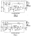
- a second approach is to make use of a more complex volt-second clamp architecture that typically uses an analog multiplier/divider to create a current that is inversely proportional to the input voltage. This current is then used to charge a capacitor that resides within the PWM controller integrated circuit. Such a circuit is illustrated in FIG. 3 .
- a volt-second clamp circuit 30 in FIG. 3 includes an analog multiplier/divider circuit 22 that divides voltage value V BI by a voltage value produced at the node between resistors R1 and R2.
- the output of the multiplier/divider 22 controls transconductance amplifier G M . coupled to the positive input of the comparator U1, together with switch M2 and integrated circuit capacitor C.
- Voltage V B2 is supplied to the transconductance amplifier G M .
- a DC/DC conversion system configured for producing an output voltage in response to an input voltage has a transformer with a primary winding responsive to the input voltage, and a secondary winding for producing the output voltage.
- the conversion system comprises a power switch coupled to the primary winding of the transformer and controlled with a converter control signal, such as a PWM control signal.
- the power switch is further controlled by a comparator that compares an input value supplied to its input with a variable reference value so as to prevent magnetic flux density of the transformer from increasing to an undesired level.
- the input value of the comparator is produced by a comparator input circuit as a function of the input voltage and an on-time of the power switch.
- the variable reference value produced by a reference circuit varies as a function of the input voltage.
- the reference circuit may be configured for producing the variable reference value based on a reference adjustment value inversely proportional to the input voltage.
- the reference adjustment value may be produced by dividing a pre-selected constant value by a value of the input voltage.
- the reference circuit may subtract the reference adjustment value from a fixed reference value to produce the variable reference value.
- the comparator may be arranged on a chip, such as a converter controller chip, and the comparator input circuit may include a capacitor arranged externally with respect to the chip.
- a switch responsive to an output signal of the comparator may control charging and discharging of the capacitor.
- a control system for controlling a circuit having a transformer arranged between input circuitry and output circuitry to galvanically isolate the output circuitry from the input circuitry.
- the control system comprises a power switch controlled to apply voltage to the transformer, and a switch control circuit responsive to a difference between a variable control value and a variable reference value to control the power switch so as to control the voltage applied to the transformer.
- the control value is produced as a function of the voltage applied to the transformer and an on-time of the switch.
- the reference value varies as a function of the voltage applied to the transformer.
- variable reference value may be produced by a reference circuit based on a reference adjustment value inversely proportional to the voltage applied to the transformer.
- the reference adjustment value may be generated by dividing a pre-selected constant value by a value of the voltage applied to the transformer.
- the reference adjustment value may be subtracted from a fixed reference value to produce the variable reference value.
- the switch control circuit may be arranged on a chip, and the control value generating circuit may include a capacitor arranged externally with respect to the chip.
- the control value generating circuit may further include a switch responsive to an output signal of the switch control circuit to control charging of the capacitor.
- the following steps are carried out to limit magnetic flux density in a transformer used to galvanically isolate an output of a DC/DC converter from an input voltage:
- the variable reference value may be produced based on a reference adjustment value inversely proportional to the input voltage.
- the reference adjustment value may be generated by dividing a pre-selected constant value by the value of the input voltage.
- the variable reference value may be produced by subtracting the reference adjustment value from a fixed reference value.
- the present disclosure will be made using an exemplary arrangement of a volt-second clamp circuit coupled to the primary winding of a power transformer in an isolated DC/DC converter. It will become apparent, however, that the concepts described herein are applicable to any volt-second clamp arrangement coupled to either a primary or a secondary winding of a transformer arranged in any circuit configuration.
- FIG. 4 illustrates an exemplary embodiment of a volt-second clamp circuit 40 of the present disclosure.
- the volt-clamp circuit 40 may be provided on a converter controller IC, such as a PWM controller IC, configured for controlling an isolated DC/DC converter having a power transformer T1 that provides galvanic isolation of secondary side circuitry coupled to the secondary winding of the transformer T1 from primary side circuitry coupled to the primary winding of the transformer T1.
- a power switch M1 such as a MOSFET, may be coupled to the primary winding so as to allow input voltage V IN of the converter to apply to the transformer T1 when M1 is on.
- the volt-second clamp circuit 40 may include a voltage comparator U1 for comparing a value at its positive input with a reference value at its negative input.
- the output of the comparator-U1 is coupled to a reset input R of a latch U2.
- a set input S/ of the latch U2 is supplied with a PWM control signal.
- the output Q of the latch U2 is coupled to one input of an AND gate G1.
- Another input of the AND gate G1 is supplied with the PWM control signal.
- the output of the AND gate G1 is supplied to the switch M1 to control its switching. Via an inverter G2, the output signal of the AND gate G1 is also supplied to control switching of a switch M2 coupled to the positive input of the comparator U 1.
- the switch M2 controls charging of an RC charging circuit composed of a resistor R and capacitor C arranged externally with respect to the converter controller IC. A node connecting the resistor R and capacitor C is coupled to the positive input of the comparator U1.
- the comparator U1 controls the switch M1 so as to limit the on-time of this switch.
- the switch M1 is on and voltage V IN is applied to the transformer T1
- the switch M2 is off and the external RC circuit is allowed to charge, increasing the voltage at the positive input of the comparator U1. If this voltage exceeds a reference voltage supplied to the negative input of the comparator U1, the output of the comparator U1 goes high indicating that the volt-second limit has been reached.
- the output signal of the comparator U1 resets latch U2 that causes the switch M1 to turn off even if the PWM signal is still high.
- the switch M1 is off, the switch M2 is on, discharging the capacitor C in the RC charging circuit coupled to the positive input of the comparator U1.
- the signal at the positive input of the comparator U1 is produced as a function of the input voltage V IN and the on-time of the switch M1.
- a value of the reference voltage supplied to the negative input of the comparator U1 may vary as a function of the input voltage V IN .
- a value of the reference voltage V R may correspond to a value of fixed reference voltage V R1 adjusted by a value inversely proportional to the input voltage V IN .
- V R V IN 1 ⁇ e ⁇ V RI V IN
- V RI is a fixed reference voltage
- V R V R 1 ⁇ K V IN
- V R1 is a fixed reference voltage
- K is a constant that can be calculated or empirically determined for a best fit approximation to the exponential.
- V R1 is a fixed reference voltage
- K is a constant that can be calculated or empirically determined for a best fit approximation to the exponential.
- a reference voltage typically within 1% of the desired exponential ideal.
- V IN varies between 1.5V and 10V
- V R1 of 0.6V a fixed reference voltage
- the produced value C is supplied to an adder/subtractor circuit 44 that subtracts the value C from a fixed reference value V R1.
- the output of the adder/subtractor circuit 44 represents the variable reference value V R supplied to the negative input of the comparator U1.
- the volt-second claim circuit of the present disclosure compares a value at the input of the comparator U1 with a variable reference value V R produced as a function of the input voltage V IN , for example, by adjusting a fixed reference value V R1 by an amount inversely proportional to the input voltage V IN .
- the accuracy of the clamp is only minimally impacted when the input voltage V IN gets low relative to the reference voltage V R .
- Prior art approaches use an analog multiplier to replace the entire RC charging circuit, thereby introducing unnecessary inaccuracies.
- the multiplier/divider is only used to create a correction to the reference voltage, so that the accuracy of the multiplier/divider is not especially critical.
- the volt-second clamp of the present disclosure does not suffer from the inaccuracy associated with an integrated circuit capacitor.
- the circuit response is essentially instantaneous, maintaining a cycle-by-cycle control of the volt-seconds applied to the transformer T1.
- FIG. 4 shows a volt-second clamp circuit provided on the primary side of the transformer T1
- the present disclosure is also applicable to improving the accuracy of a volt-second clamp circuit arranged at the secondary side of the transformer T1, such as a circuit illustrated in FIG. 2 .
Landscapes
- Engineering & Computer Science (AREA)
- Power Engineering (AREA)
- Dc-Dc Converters (AREA)
Claims (8)
- Ein DC/DC-Wandlungssystem bzw. Gleichstromwandlersystem, das dazu konfiguriert ist, als Antwort auf eine Eingangsspannung eine Ausgangsspannung zu erzeugen, und das einen Transformator mit einer primären Wicklung aufweist, die auf die Eingangsspannung anspricht, und eine sekundäre Wicklung, um die Ausgangsspannung zu erzeugen, wobei das System Folgendes umfasst:einen Leistungsschalter, der mit der Primärwicklung des Transformators gekoppelt ist und mit einem Steuersignal des Wandlers gesteuert wird,einen Komparator bzw. Vergleicher, um einen Eingangswert, der dem Komparator zugeführt wird, mit einem variablen Referenzwert zur Steuerung des Leistungsschalters zu vergleichen, sodass vermieden wird, dass die magnetische Flussdichte des Transformators unerwünscht hohe Werte erreicht,einen Komparator-Eingangs-Schaltkreis zur Erzeugung des Eingangswertes des Komparators als Funktion der Eingangsspannung und einer Einschaltzeit des Leistungsschalters, undeine Referenzschaltung, um den variablen Referenzwert zu erzeugen, indem eine feste Referenzspannung um einen Referenz-Einstellwert angepasst wird, der umgekehrt proportional zur Eingangsspannung ist.
- Das System nach Anspruch 1, wobei die Referenzschaltung konfiguriert ist, um den Referenz-Einstellwert zu erzeugen, indem ein vorgewählter konstanter Wert durch einen Wert der Eingangsspannung dividiert wird.
- Das System nach Anspruch 1 oder 2, wobei die Referenzschaltung konfiguriert ist, um Referenz-Einstellwert von der festen Referenzspannung zu subtrahieren, um den variablen Referenzwert zu erzeugen.
- Das System nach irgendeinem der Ansprüche 1 bis 3, wobei der Komparator auf einem integrierten Schaltkreis angeordnet ist, und der Komparator-Eingangs-Schaltkreis einen Kondensator beinhaltet, der in Bezug auf den integrierten Schaltkreis außen angeordnet ist.
- Das System nach Anspruch 4, wobei der Komparator-Eingangs-Schaltkreis des Weiteren einen Umschalter beinhaltet, der auf ein Ausgangssignal des Komparators reagiert, um den Ladevorgang des Kondensators zu steuern.
- Ein Verfahren zur Beschränkung der magnetischen Flussdichte in einem Transformator, der verwendet wird, um einen Ausgang eines DC/DC-Wandlers von einer Eingangsspannung galvanisch zu trennen, wobei das Verfahren die folgenden Schritte umfasst:erzeugen eines Steuerwertes als Funktion der Eingangsspannung und einer Einschaltzeit eines Umschalters bzw. Schalters, der den DC/DC-Wandler steuert,erzeugen eines variablen Referenzwertes, indem eine feste Referenzspannung um einen Referenz-Einstellwert angepasst wird, der zur Eingangsspannung umgekehrt proportional ist, undbasierend auf einer Differenz zwischen dem Steuerwert und dem variablen Referenzwert, steuern der Zufuhr der Eingangsspannung an den Transformator.
- Das Verfahren nach Anspruch 6, wobei der Referenz-Einstellwert erzeugt wird, indem ein vorgewählter konstanter Wert durch einen Wert der Eingangsspannung dividiert wird.
- Das Verfahren nach Anspruch 6 oder 7, wobei der variable Referenzwert erzeugt wird, indem der Referenz-Einstellwert von der festen Referenzspannung subtrahiert wird.
Priority Applications (1)
| Application Number | Priority Date | Filing Date | Title |
|---|---|---|---|
| EP16001187.0A EP3091650A1 (de) | 2009-09-17 | 2010-09-17 | Verbesserung der genauigkeit einer voltsekundenklemme in einem isolierten gleichstromwandler |
Applications Claiming Priority (1)
| Application Number | Priority Date | Filing Date | Title |
|---|---|---|---|
| US24323009P | 2009-09-17 | 2009-09-17 |
Related Child Applications (1)
| Application Number | Title | Priority Date | Filing Date |
|---|---|---|---|
| EP16001187.0A Division EP3091650A1 (de) | 2009-09-17 | 2010-09-17 | Verbesserung der genauigkeit einer voltsekundenklemme in einem isolierten gleichstromwandler |
Publications (2)
| Publication Number | Publication Date |
|---|---|
| EP2299573A1 EP2299573A1 (de) | 2011-03-23 |
| EP2299573B1 true EP2299573B1 (de) | 2016-05-25 |
Family
ID=43413504
Family Applications (2)
| Application Number | Title | Priority Date | Filing Date |
|---|---|---|---|
| EP16001187.0A Withdrawn EP3091650A1 (de) | 2009-09-17 | 2010-09-17 | Verbesserung der genauigkeit einer voltsekundenklemme in einem isolierten gleichstromwandler |
| EP10009842.5A Active EP2299573B1 (de) | 2009-09-17 | 2010-09-17 | Verbesserung der Genauigkeit einer Volt-Second-Clamp in einem isolierten Gleichstromwandler |
Family Applications Before (1)
| Application Number | Title | Priority Date | Filing Date |
|---|---|---|---|
| EP16001187.0A Withdrawn EP3091650A1 (de) | 2009-09-17 | 2010-09-17 | Verbesserung der genauigkeit einer voltsekundenklemme in einem isolierten gleichstromwandler |
Country Status (2)
| Country | Link |
|---|---|
| US (1) | US8593839B2 (de) |
| EP (2) | EP3091650A1 (de) |
Families Citing this family (5)
| Publication number | Priority date | Publication date | Assignee | Title |
|---|---|---|---|---|
| US8934267B2 (en) * | 2010-11-09 | 2015-01-13 | Tdk-Lambda Corporation | Loosely regulated feedback control for high efficiency isolated DC-DC converters |
| US9520772B2 (en) | 2010-11-09 | 2016-12-13 | Tdk-Lambda Corporation | Multi-level voltage regulator system |
| CN105490545B (zh) * | 2014-09-19 | 2018-07-13 | 万国半导体(开曼)股份有限公司 | 固定导通时间切换式转换装置 |
| US11632054B2 (en) | 2019-04-24 | 2023-04-18 | Power Integrations, Inc. | Mode operation detection for control of a power converter with an active clamp switch |
| EP3959807B1 (de) * | 2019-04-24 | 2023-06-07 | Power Integrations, Inc. | Leistungsumrichter mit einer aktiven nicht dissipativen klemmschaltung, und zugehörige regelschaltung |
Citations (1)
| Publication number | Priority date | Publication date | Assignee | Title |
|---|---|---|---|---|
| US20090161287A1 (en) * | 2007-12-19 | 2009-06-25 | Freescale Semiconductor, Inc. | Electronic device operable to protect a power transistor when used in conjunction with a transformer |
Family Cites Families (11)
| Publication number | Priority date | Publication date | Assignee | Title |
|---|---|---|---|---|
| US552979A (en) * | 1896-01-14 | Joseph baker | ||
| US4477867A (en) * | 1981-08-28 | 1984-10-16 | Data General Corporation | Core saturation control circuit |
| US4794508A (en) * | 1987-12-23 | 1988-12-27 | Dci Technology | PWM control circuit for a non-symmetrical switching power supply |
| DE58907794D1 (de) * | 1989-09-19 | 1994-07-07 | Siemens Ag | Verfahren und Schaltungsanordnung zum Ansteuern eines Halbleiterschalters unter Verwendung eines induktiven Übertragers. |
| US5552979A (en) | 1993-11-30 | 1996-09-03 | Philips Electronics North America Corporation | Isolated current sensor for DC to high frequency applications |
| US5710697A (en) | 1996-03-26 | 1998-01-20 | Unitrode Corporation | Power supply controller having frequency foldback and volt-second duty cycle clamp features |
| US6327178B1 (en) | 2000-07-18 | 2001-12-04 | Micron Technology, Inc. | Programmable circuit and its method of operation |
| GB2370655B (en) | 2000-07-18 | 2005-01-19 | Coutant Lambda Ltd | A DC switching regulator |
| TW538589B (en) * | 2001-07-13 | 2003-06-21 | Delta Electronics Inc | Volt-second clamping circuit power supplier |
| US6717826B2 (en) * | 2002-01-31 | 2004-04-06 | Texas Instruments Incorporated | Method to reduce bus voltage stress in a single-stage single switch power factor correction circuit |
| US8139384B2 (en) * | 2009-06-02 | 2012-03-20 | Power Integrations, Inc. | Method and apparatus for input charge control of a power supply |
-
2010
- 2010-09-15 US US12/882,806 patent/US8593839B2/en active Active
- 2010-09-17 EP EP16001187.0A patent/EP3091650A1/de not_active Withdrawn
- 2010-09-17 EP EP10009842.5A patent/EP2299573B1/de active Active
Patent Citations (1)
| Publication number | Priority date | Publication date | Assignee | Title |
|---|---|---|---|---|
| US20090161287A1 (en) * | 2007-12-19 | 2009-06-25 | Freescale Semiconductor, Inc. | Electronic device operable to protect a power transistor when used in conjunction with a transformer |
Also Published As
| Publication number | Publication date |
|---|---|
| US20110063882A1 (en) | 2011-03-17 |
| EP3091650A1 (de) | 2016-11-09 |
| EP2299573A1 (de) | 2011-03-23 |
| US8593839B2 (en) | 2013-11-26 |
Similar Documents
| Publication | Publication Date | Title |
|---|---|---|
| US8148968B2 (en) | Method and apparatus for a power supply controller responsive to a feedforward signal | |
| US9391523B2 (en) | Controller with constant current limit | |
| US9088217B2 (en) | Systems and methods for load compensation with primary-side sensing and regulation for flyback power converters | |
| US10236680B2 (en) | Control circuit of switching power supply device | |
| US8248826B2 (en) | Method for controlling a switching regulator and related switching regulator | |
| EP2987230B1 (de) | System und verfahren zum regeln von gleichrichtern auf der basis von mehrpunkt-hochsetzstellern zur leistungsfaktorkorrektur | |
| EP1969705B1 (de) | Schaltregler-steigungskompensationsgeneratorschaltung | |
| US20080246447A1 (en) | Method and apparatus for integrated cable drop compensation of a power converter | |
| US20140268920A1 (en) | Systems and Methods for Flyback Power Converters with Switching Frequency and Peak Current Adjustments | |
| US11183937B2 (en) | Digitally compensated current sensing protection | |
| US20120294052A1 (en) | Monotonic pre-bias start-up of a dc-dc converter | |
| KR20140113521A (ko) | Dc-dc 컨버터의 제어 방법 및 제어 시스템 | |
| EP3518407B1 (de) | Vorrichtung und verfahren zur linearisierung der steuerung von steuerungseingaben für einen resonanzwandler mit zwei ausgängen | |
| EP2299573B1 (de) | Verbesserung der Genauigkeit einer Volt-Second-Clamp in einem isolierten Gleichstromwandler | |
| US20110194316A1 (en) | Switching power supply device | |
| US5986911A (en) | Secondary side post regulator and multiple output power supply employing the same | |
| US11223273B2 (en) | Sub-harmonic oscillation control in peak current limit mode switching system | |
| US12068693B2 (en) | Digital nonlinear transformation for voltage-mode control of a power converter | |
| US20220158536A1 (en) | Soft-start for resonant converters | |
| EP3518409B1 (de) | Vorrichtung und verfahren für einen doppelausgangsresonanzwandler zur sicherstellung des vollen leistungsbereichs für beide ausgänge | |
| US9397560B2 (en) | Controller for a power supply with transition region regulation | |
| JPH0783587B2 (ja) | Dc―dcコンバータの過電流制限方法 | |
| EP3035515A1 (de) | Isolierter Gleichspannungswandler |
Legal Events
| Date | Code | Title | Description |
|---|---|---|---|
| PUAI | Public reference made under article 153(3) epc to a published international application that has entered the european phase |
Free format text: ORIGINAL CODE: 0009012 |
|
| AK | Designated contracting states |
Kind code of ref document: A1 Designated state(s): AL AT BE BG CH CY CZ DE DK EE ES FI FR GB GR HR HU IE IS IT LI LT LU LV MC MK MT NL NO PL PT RO SE SI SK SM TR |
|
| AX | Request for extension of the european patent |
Extension state: BA ME RS |
|
| RAP1 | Party data changed (applicant data changed or rights of an application transferred) |
Owner name: LINEAR TECHNOLOGY CORPORATION |
|
| 17P | Request for examination filed |
Effective date: 20110922 |
|
| 17Q | First examination report despatched |
Effective date: 20120208 |
|
| GRAP | Despatch of communication of intention to grant a patent |
Free format text: ORIGINAL CODE: EPIDOSNIGR1 |
|
| INTG | Intention to grant announced |
Effective date: 20151209 |
|
| GRAS | Grant fee paid |
Free format text: ORIGINAL CODE: EPIDOSNIGR3 |
|
| GRAA | (expected) grant |
Free format text: ORIGINAL CODE: 0009210 |
|
| RIN1 | Information on inventor provided before grant (corrected) |
Inventor name: HAWKES, CHARLES EDWARD |
|
| AK | Designated contracting states |
Kind code of ref document: B1 Designated state(s): AL AT BE BG CH CY CZ DE DK EE ES FI FR GB GR HR HU IE IS IT LI LT LU LV MC MK MT NL NO PL PT RO SE SI SK SM TR |
|
| REG | Reference to a national code |
Ref country code: GB Ref legal event code: FG4D |
|
| REG | Reference to a national code |
Ref country code: CH Ref legal event code: EP |
|
| REG | Reference to a national code |
Ref country code: AT Ref legal event code: REF Ref document number: 803052 Country of ref document: AT Kind code of ref document: T Effective date: 20160615 Ref country code: IE Ref legal event code: FG4D |
|
| REG | Reference to a national code |
Ref country code: DE Ref legal event code: R096 Ref document number: 602010033565 Country of ref document: DE |
|
| REG | Reference to a national code |
Ref country code: NL Ref legal event code: FP |
|
| REG | Reference to a national code |
Ref country code: FR Ref legal event code: PLFP Year of fee payment: 7 Ref country code: LT Ref legal event code: MG4D |
|
| PG25 | Lapsed in a contracting state [announced via postgrant information from national office to epo] |
Ref country code: LT Free format text: LAPSE BECAUSE OF FAILURE TO SUBMIT A TRANSLATION OF THE DESCRIPTION OR TO PAY THE FEE WITHIN THE PRESCRIBED TIME-LIMIT Effective date: 20160525 Ref country code: FI Free format text: LAPSE BECAUSE OF FAILURE TO SUBMIT A TRANSLATION OF THE DESCRIPTION OR TO PAY THE FEE WITHIN THE PRESCRIBED TIME-LIMIT Effective date: 20160525 Ref country code: NO Free format text: LAPSE BECAUSE OF FAILURE TO SUBMIT A TRANSLATION OF THE DESCRIPTION OR TO PAY THE FEE WITHIN THE PRESCRIBED TIME-LIMIT Effective date: 20160825 |
|
| REG | Reference to a national code |
Ref country code: AT Ref legal event code: MK05 Ref document number: 803052 Country of ref document: AT Kind code of ref document: T Effective date: 20160525 |
|
| PG25 | Lapsed in a contracting state [announced via postgrant information from national office to epo] |
Ref country code: PT Free format text: LAPSE BECAUSE OF FAILURE TO SUBMIT A TRANSLATION OF THE DESCRIPTION OR TO PAY THE FEE WITHIN THE PRESCRIBED TIME-LIMIT Effective date: 20160926 Ref country code: ES Free format text: LAPSE BECAUSE OF FAILURE TO SUBMIT A TRANSLATION OF THE DESCRIPTION OR TO PAY THE FEE WITHIN THE PRESCRIBED TIME-LIMIT Effective date: 20160525 Ref country code: SE Free format text: LAPSE BECAUSE OF FAILURE TO SUBMIT A TRANSLATION OF THE DESCRIPTION OR TO PAY THE FEE WITHIN THE PRESCRIBED TIME-LIMIT Effective date: 20160525 Ref country code: GR Free format text: LAPSE BECAUSE OF FAILURE TO SUBMIT A TRANSLATION OF THE DESCRIPTION OR TO PAY THE FEE WITHIN THE PRESCRIBED TIME-LIMIT Effective date: 20160826 Ref country code: HR Free format text: LAPSE BECAUSE OF FAILURE TO SUBMIT A TRANSLATION OF THE DESCRIPTION OR TO PAY THE FEE WITHIN THE PRESCRIBED TIME-LIMIT Effective date: 20160525 Ref country code: LV Free format text: LAPSE BECAUSE OF FAILURE TO SUBMIT A TRANSLATION OF THE DESCRIPTION OR TO PAY THE FEE WITHIN THE PRESCRIBED TIME-LIMIT Effective date: 20160525 |
|
| PG25 | Lapsed in a contracting state [announced via postgrant information from national office to epo] |
Ref country code: CZ Free format text: LAPSE BECAUSE OF FAILURE TO SUBMIT A TRANSLATION OF THE DESCRIPTION OR TO PAY THE FEE WITHIN THE PRESCRIBED TIME-LIMIT Effective date: 20160525 Ref country code: EE Free format text: LAPSE BECAUSE OF FAILURE TO SUBMIT A TRANSLATION OF THE DESCRIPTION OR TO PAY THE FEE WITHIN THE PRESCRIBED TIME-LIMIT Effective date: 20160525 Ref country code: SK Free format text: LAPSE BECAUSE OF FAILURE TO SUBMIT A TRANSLATION OF THE DESCRIPTION OR TO PAY THE FEE WITHIN THE PRESCRIBED TIME-LIMIT Effective date: 20160525 Ref country code: DK Free format text: LAPSE BECAUSE OF FAILURE TO SUBMIT A TRANSLATION OF THE DESCRIPTION OR TO PAY THE FEE WITHIN THE PRESCRIBED TIME-LIMIT Effective date: 20160525 Ref country code: RO Free format text: LAPSE BECAUSE OF FAILURE TO SUBMIT A TRANSLATION OF THE DESCRIPTION OR TO PAY THE FEE WITHIN THE PRESCRIBED TIME-LIMIT Effective date: 20160525 |
|
| PG25 | Lapsed in a contracting state [announced via postgrant information from national office to epo] |
Ref country code: BE Free format text: LAPSE BECAUSE OF NON-PAYMENT OF DUE FEES Effective date: 20160525 Ref country code: AT Free format text: LAPSE BECAUSE OF FAILURE TO SUBMIT A TRANSLATION OF THE DESCRIPTION OR TO PAY THE FEE WITHIN THE PRESCRIBED TIME-LIMIT Effective date: 20160525 Ref country code: SM Free format text: LAPSE BECAUSE OF FAILURE TO SUBMIT A TRANSLATION OF THE DESCRIPTION OR TO PAY THE FEE WITHIN THE PRESCRIBED TIME-LIMIT Effective date: 20160525 Ref country code: PL Free format text: LAPSE BECAUSE OF FAILURE TO SUBMIT A TRANSLATION OF THE DESCRIPTION OR TO PAY THE FEE WITHIN THE PRESCRIBED TIME-LIMIT Effective date: 20160525 |
|
| REG | Reference to a national code |
Ref country code: DE Ref legal event code: R097 Ref document number: 602010033565 Country of ref document: DE |
|
| PLBE | No opposition filed within time limit |
Free format text: ORIGINAL CODE: 0009261 |
|
| STAA | Information on the status of an ep patent application or granted ep patent |
Free format text: STATUS: NO OPPOSITION FILED WITHIN TIME LIMIT |
|
| PG25 | Lapsed in a contracting state [announced via postgrant information from national office to epo] |
Ref country code: MC Free format text: LAPSE BECAUSE OF FAILURE TO SUBMIT A TRANSLATION OF THE DESCRIPTION OR TO PAY THE FEE WITHIN THE PRESCRIBED TIME-LIMIT Effective date: 20160525 |
|
| REG | Reference to a national code |
Ref country code: CH Ref legal event code: PL |
|
| 26N | No opposition filed |
Effective date: 20170228 |
|
| PG25 | Lapsed in a contracting state [announced via postgrant information from national office to epo] |
Ref country code: SI Free format text: LAPSE BECAUSE OF FAILURE TO SUBMIT A TRANSLATION OF THE DESCRIPTION OR TO PAY THE FEE WITHIN THE PRESCRIBED TIME-LIMIT Effective date: 20160525 |
|
| REG | Reference to a national code |
Ref country code: IE Ref legal event code: MM4A |
|
| PG25 | Lapsed in a contracting state [announced via postgrant information from national office to epo] |
Ref country code: IE Free format text: LAPSE BECAUSE OF NON-PAYMENT OF DUE FEES Effective date: 20160917 Ref country code: LI Free format text: LAPSE BECAUSE OF NON-PAYMENT OF DUE FEES Effective date: 20160930 Ref country code: CH Free format text: LAPSE BECAUSE OF NON-PAYMENT OF DUE FEES Effective date: 20160930 |
|
| PG25 | Lapsed in a contracting state [announced via postgrant information from national office to epo] |
Ref country code: LU Free format text: LAPSE BECAUSE OF NON-PAYMENT OF DUE FEES Effective date: 20160917 |
|
| REG | Reference to a national code |
Ref country code: FR Ref legal event code: PLFP Year of fee payment: 8 |
|
| PG25 | Lapsed in a contracting state [announced via postgrant information from national office to epo] |
Ref country code: HU Free format text: LAPSE BECAUSE OF FAILURE TO SUBMIT A TRANSLATION OF THE DESCRIPTION OR TO PAY THE FEE WITHIN THE PRESCRIBED TIME-LIMIT; INVALID AB INITIO Effective date: 20100917 Ref country code: CY Free format text: LAPSE BECAUSE OF FAILURE TO SUBMIT A TRANSLATION OF THE DESCRIPTION OR TO PAY THE FEE WITHIN THE PRESCRIBED TIME-LIMIT Effective date: 20160525 |
|
| PG25 | Lapsed in a contracting state [announced via postgrant information from national office to epo] |
Ref country code: MT Free format text: LAPSE BECAUSE OF NON-PAYMENT OF DUE FEES Effective date: 20160930 Ref country code: TR Free format text: LAPSE BECAUSE OF FAILURE TO SUBMIT A TRANSLATION OF THE DESCRIPTION OR TO PAY THE FEE WITHIN THE PRESCRIBED TIME-LIMIT Effective date: 20160525 Ref country code: IS Free format text: LAPSE BECAUSE OF FAILURE TO SUBMIT A TRANSLATION OF THE DESCRIPTION OR TO PAY THE FEE WITHIN THE PRESCRIBED TIME-LIMIT Effective date: 20160525 Ref country code: MK Free format text: LAPSE BECAUSE OF FAILURE TO SUBMIT A TRANSLATION OF THE DESCRIPTION OR TO PAY THE FEE WITHIN THE PRESCRIBED TIME-LIMIT Effective date: 20160525 |
|
| PG25 | Lapsed in a contracting state [announced via postgrant information from national office to epo] |
Ref country code: BG Free format text: LAPSE BECAUSE OF FAILURE TO SUBMIT A TRANSLATION OF THE DESCRIPTION OR TO PAY THE FEE WITHIN THE PRESCRIBED TIME-LIMIT Effective date: 20160525 |
|
| REG | Reference to a national code |
Ref country code: FR Ref legal event code: PLFP Year of fee payment: 9 |
|
| PG25 | Lapsed in a contracting state [announced via postgrant information from national office to epo] |
Ref country code: AL Free format text: LAPSE BECAUSE OF FAILURE TO SUBMIT A TRANSLATION OF THE DESCRIPTION OR TO PAY THE FEE WITHIN THE PRESCRIBED TIME-LIMIT Effective date: 20160525 |
|
| REG | Reference to a national code |
Ref country code: DE Ref legal event code: R082 Ref document number: 602010033565 Country of ref document: DE Representative=s name: WITHERS & ROGERS LLP, DE Ref country code: DE Ref legal event code: R082 Ref document number: 602010033565 Country of ref document: DE Representative=s name: MUELLER-BORE & PARTNER PATENTANWAELTE PARTG MB, DE Ref country code: DE Ref legal event code: R081 Ref document number: 602010033565 Country of ref document: DE Owner name: ANALOG DEVICES INTERNATIONAL UNLIMITED COMPANY, IE Free format text: FORMER OWNER: LINEAR TECHNOLOGY CORPORATION, MILPITAS, CALIF., US |
|
| REG | Reference to a national code |
Ref country code: DE Ref legal event code: R082 Ref document number: 602010033565 Country of ref document: DE Representative=s name: WITHERS & ROGERS LLP, DE |
|
| PGFP | Annual fee paid to national office [announced via postgrant information from national office to epo] |
Ref country code: IT Payment date: 20210824 Year of fee payment: 12 |
|
| REG | Reference to a national code |
Ref country code: GB Ref legal event code: 732E Free format text: REGISTERED BETWEEN 20211125 AND 20211201 |
|
| REG | Reference to a national code |
Ref country code: NL Ref legal event code: PD Owner name: ANALOG DEVICES INTERNATIONAL UNLIMITED COMPANY; IE Free format text: DETAILS ASSIGNMENT: CHANGE OF OWNER(S), ASSIGNMENT; FORMER OWNER NAME: LINEAR TECHNOLOGY LLC Effective date: 20211216 |
|
| PG25 | Lapsed in a contracting state [announced via postgrant information from national office to epo] |
Ref country code: IT Free format text: LAPSE BECAUSE OF NON-PAYMENT OF DUE FEES Effective date: 20220917 |
|
| PGFP | Annual fee paid to national office [announced via postgrant information from national office to epo] |
Ref country code: NL Payment date: 20240820 Year of fee payment: 15 |
|
| PGFP | Annual fee paid to national office [announced via postgrant information from national office to epo] |
Ref country code: DE Payment date: 20240820 Year of fee payment: 15 |
|
| PGFP | Annual fee paid to national office [announced via postgrant information from national office to epo] |
Ref country code: GB Payment date: 20240821 Year of fee payment: 15 |
|
| PGFP | Annual fee paid to national office [announced via postgrant information from national office to epo] |
Ref country code: FR Payment date: 20240820 Year of fee payment: 15 |