EP2299570A2 - Dc/dc converter overcurrent protection - Google Patents
Dc/dc converter overcurrent protection Download PDFInfo
- Publication number
- EP2299570A2 EP2299570A2 EP10009844A EP10009844A EP2299570A2 EP 2299570 A2 EP2299570 A2 EP 2299570A2 EP 10009844 A EP10009844 A EP 10009844A EP 10009844 A EP10009844 A EP 10009844A EP 2299570 A2 EP2299570 A2 EP 2299570A2
- Authority
- EP
- European Patent Office
- Prior art keywords
- mosfet
- converter
- output
- current
- sense resistor
- Prior art date
- Legal status (The legal status is an assumption and is not a legal conclusion. Google has not performed a legal analysis and makes no representation as to the accuracy of the status listed.)
- Granted
Links
Images


Classifications
-
- H—ELECTRICITY
- H02—GENERATION; CONVERSION OR DISTRIBUTION OF ELECTRIC POWER
- H02M—APPARATUS FOR CONVERSION BETWEEN AC AND AC, BETWEEN AC AND DC, OR BETWEEN DC AND DC, AND FOR USE WITH MAINS OR SIMILAR POWER SUPPLY SYSTEMS; CONVERSION OF DC OR AC INPUT POWER INTO SURGE OUTPUT POWER; CONTROL OR REGULATION THEREOF
- H02M1/00—Details of apparatus for conversion
- H02M1/32—Means for protecting converters other than automatic disconnection
-
- H—ELECTRICITY
- H02—GENERATION; CONVERSION OR DISTRIBUTION OF ELECTRIC POWER
- H02M—APPARATUS FOR CONVERSION BETWEEN AC AND AC, BETWEEN AC AND DC, OR BETWEEN DC AND DC, AND FOR USE WITH MAINS OR SIMILAR POWER SUPPLY SYSTEMS; CONVERSION OF DC OR AC INPUT POWER INTO SURGE OUTPUT POWER; CONTROL OR REGULATION THEREOF
- H02M3/00—Conversion of DC power input into DC power output
Definitions
- the present disclosure relates generally to DC/DC converters, and more particularly to a DC/DC converter provided with overcurrent protection.
- DC/DC converters are widely used to step from an input voltage level to an output voltage level that may be higher or lower than the input voltage. These converters generally use pulse-width modulated MOSFET switches to convert one DC voltage to another with minimal power loss. Protecting the MOSFET switches and other circuit components from destructive overcurrent conditions is necessary to ensure reliable and safe operation.
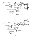
- DC/DC converters often include provisions for overcurrent protection. Often the DC/DC converter is provided in the form of an integrated chip, and is used to protect a transistor such as a MOSFET from overcurrent conditions. As an example, as shown in Figure 1 , a DC/DC converter 10 (only a portion of which is shown in Figure 1 for ease of illustration and explanation) can be connected to a MOSFET 12 that requires overcurrent protection by connecting the gate of the MOSFET to the pin 16. In this case a solution to provide overcurrent protection also requires connecting at least one other external pin 18 of the converter 10 to a resistor 14, which in turn is connected in series with the source of the MOSFET 12. The current through the MOSFET 12 is measured by sensing the voltage across resistor 14.
- a comparator 20 of the converter is used to compare the sensed voltage across external resistor 14 to a fixed internal reference voltage V OS . As long as the sensed voltage is less than V OS the converter 20 will continue to operate under the condition that the MOSFET 12 is operating within its current limit. However, should the current through the MOSFET 12 exceed the current limit, the voltage across resistor 14 will exceed the reference voltage V OS and the comparator will provide a leading edge of a pulse to the reset input R of the latch 22 so as to the cause the Q output of the latch to go low. The low output is applied to the AND gate so that the output of the gate will go low until the next cycle. The low output results in the output at pin 16 low so as to turn the MOSFET 12 off.
- Figure 2 shows the prior art approach is sensing the current through the resistor using two pins 18 and 24.
- Single-ended sensing has the advantage of requiring one less pin; however, special care must be taken with the ground sense of the comparator to ensure signal integrity. That is, any difference between the ground on the bottom side of the sense resistor and the ground of the overcurrent comparator will appear as an offset that causes the overcurrent comparator to trip prematurely or, worse yet, not to trip when a true overcurrent event occurs.
- Both arrangements typically include a blanking circuit 26 so that both the single-ended and differential sense methods typically disable, or "Blank,” the overcurrent comparator for a few hundred nanoseconds after turning on the MOSFET to avoid a false overcurrent trip due to noise.
- problems of this prior art approach include the need to provide one or two external pins dedicated solely to the implementation of overcurrent protection, which increases IC package size, package cost, and PCB area. Special care must be taken with signal routing, particularly in the single-ended sense configuration, since noise and unintended resistance in the current sense path may cause the overcurrent comparator to trip prematurely or not trip in an overcurrent condition.
- the overcurrent comparator input is limited to a specific common-mode voltage range, and can not be used at arbitrarily high or low voltages.
- a DC/DC converter is of a type that provides a pulse width modulated signal output signal to the gate of a MOSFET switch.
- the converter comprises: an output configured to be coupled to the gate of the MOSFET switch; and a control configured so as to sense a current generated at the output when the current through the MOSFET switch exceeds a first threshold level, and disabling the pulse width modulated output signal until the next cycle of the signal when the output current exceeds a second threshold level.
- a method for protecting a MOSFET switch coupled to the pulse width modulated output of a DC/DC converter from an overcurrent condition.
- the method comprises: coupling the MOSFET switch to a sense resistor so that current flowing though the MOSFET switch also flows through the sense resistor; coupling a bipolar transistor to the MOSFET switch and sense resistor so that current through the sense resistor biases the bipolar transistor so that when the when the current through the sense resistor exceeds a first threshold level, the bipolar transistor turns on so as to draw current from the output of the DC/DC converter; and disabling the output of the DC/DC converter until the next cycle of the pulse width modulated output when the current drawn from the output of the DC/DC converter exceeds a second threshold level.
- Figure 1 is a partial schematic, partial block diagram of a prior art approach to providing overcurrent protection when connecting a DC/DC converter to a MOSFET, requiring one dedicated pin for making an external connection;
- Figure 2 is a partial schematic, partial block diagram of a prior art approach to providing overcurrent protection when connecting a DC/DC converter to a MOSFET, requiring two dedicated pins for making an external connection;
- Figure 3 is a partial schematic, partial block diagram of one embodiment for providing overcurrent protection when connecting a DC/DC converter to a MOSFET eliminating the need for dedicated pins for making an external connection;
- Figure 4 is a partial schematic, partial block diagram of a second embodiment for providing overcurrent protection when connecting a DC/DC converter to a MOSFET eliminating the need for dedicated pins for making an external connection;
- Figure 5 is a partial schematic, partial block diagram of a third embodiment for providing overcurrent protection when connecting a DC/DC converter to a MOSFET eliminating the need for dedicated pins for making an external connection;
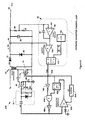
- Figure 6 is a partial schematic, partial block diagram of a more detailed exemplary embodiment a DC/DC converter incorporating the embodiment of Figure 5 for connecting the converter to a MOSFET for eliminating the need for dedicated pins for making the external connection.
- the converter 40 receives a pulse width modulated signal at node 42 which is applied to an input of AND gate 44 and the S - input of latch 46.
- the Q output of latch 46 is connected to a second input of AND gate 44.
- the output of AND gate 44 is connected to an input of output stage 48, which as described below includes a P-channel MOSFET (not specifically shown).
- the output of stage 48 is connected to the pin 50 and to an inverting input of overcurrent comparator 52, which in turn has its non-inverting input connected to receive an internal reference signal V OS -V CC and its output connect is connected the R input of latch 46.
- node 42 is connected to the blanking circuit 54, which in turn is connected to the comparator 52.
- converter 40 is connected through the pin 50 to the gate of an external N-channel MOSFET 56, which provision is made to protect from an overcurrent condition.
- the source of MOSFET 56 is connected to external sense resistor 58, and is also to the base of NPN (bipolar) transistor 60.
- the collector of NPN transistor 60 is connected to the gate of MOSFET 56, while the emitter of transistor 60 is connected to sense resistor 58 at system ground.
- current that flows through the external N-Channel MOSFET 56 also flows through the external sense resistor 58. This creates a voltage between the base and emitter of NPN transistor 60.
- NPN transistor 60 turns on and pulls a current Ic out of the gate drive output stage 48.
- Output stage 48 is held to Vcc by a P-Channel MOSFET (not shown) which has a known ON-resistance, R DS(ON) .
- the current Ic flowing through this P-channel MOSFET ON-resistance creates a voltage on the inverting input of comparator 52 equal to Vcc-Ic*R DS ( ON ).
- Comparator 52 compares this voltage to the internal reference voltage (a second threshold) on its non-inverting input, Vcc-Vos.
- the single pin approach can be extended to protecting a P-Channel MOSFET 64 gate driver as shown in Figure 4 .
- the source is connected to sense resistor 66, which in turn is connected to voltage source Vcc.
- NPN transistor 60 has been replaced with a PNP (bipolar) transistor 68.
- PNP transistor 68 has it collector connected to the pin 50A and gate of MOSFET 64.
- the base of PNP transistor 68 is connected to the source of MOSFET 64 and sense resistor 66.
- the emitter of PNP transistor 68 is connected to the voltage source Vcc and the resistor 66.
- the gate drive output of output stage 48A is inverted as shown, so that it is low when the P-Channel MOSFET 64 is "ON.”
- the overcurrent comparator 52A is now referenced to ground instead of Vcc.
- This circuit operates similarly to the circuit of Figure 3 . Specifically, current that is flowing through the external P-Channel MOSFET 64 also flows through the sense resistor 66. This creates a voltage between the emitter and base of PNP transistor 68. When this voltage reaches approximately 0.7V, the PNP transistor 68 turns on and pushes a current Ic into the gate drive output stage 48A.
- Output stage 48A is held at system ground by a N-Channel MOSFET (not shown) which has a known on-resistance, R OS(ON) .
- the current Ic flowing through the N-channel MOSFET on-resistance creates a voltage on the non-inverting input of comparator 52A equal to I C *R DS(ON) .
- Overcurrent comparator 52A compares this voltage to the voltage on its inverting input, Vos. When I C *R DS(ON) exceeds Vos, the output of comparator 52A goes high which trips latch 46A, latching the gate drive output at pin 50A low until the next PWM cycle.
- Blanking circuit 54A keeps the comparator 52A in an untripped state during switch transitions to avoid false trips due to noise.
- the teachings provided in this disclosure can be extended to other types of MOSFET configurations.
- the teachings are extended to a level-shift MOSFET 64.
- a level-shift network in configured between the pin 50A and the gate of the MOSFET 64.
- the level-shift network 70 includes a capacitor 72 connected between pin 50A gate of MOSFET 64 and the collector of bipolar transistor 68.
- a resistor 74 and the anode of Schottky diode 76 are each connected at the node formed by the capacitor 72, the collector of transistor 68 and the gate of MOSFET 64.
- the resistor 74 and the cathode of Schottky diode 76 references the P-Channel MOSFET to a voltage Vx, which may be higher or lower than Vcc.
- Vx voltage
- This level-shift network is widely used in forward converters with active clamp reset, where the voltage Vx is commonly connected to ground.
- the circuit in Figure 5 operates as follows:
- the resistor and diode in network 70 establish a reference voltage point Vx for the MOSFET 64.
- Vx the reference voltage point for the MOSFET 64.
- the gate drive output at pin 50A switches from Vcc to ground
- the gate of the MOSFET 64 is capacitively pulled low by the level-shift network 70, to a voltage of approximately equal to Vx-Vcc, turning on the MOSFET 64.
- the rest of the operation of this circuit is identical to that of Figure 4 , with the exception that the current Ic from the PNP transistor 68 is now capacitively coupled to the gate drive at pin 50A through the same level-shift network 70.
- the Vx voltage can be arbitrarily high or low and is limited only by the voltage rating of the level-shift capacitor 72 in network 70.
- FIG. 6 is a more complete diagram of an embodiment of a DC/DC converter 40B incorporating the configuration described in connection with Figure 5 .
- Vin provides voltage to the primary winding of a power transformer 72 which is connected through capacitor 74 to the drain of MOSFET 64.
- the primary winding of the transformer 72 is also applied to the drain of MOSFET 76.
- MOSFET 76 has its gate connected to the pulse-width modulated control signal (PWM) and its source connected to the system ground.
- PWM pulse-width modulated control signal
- the secondary winding of a power transformer 72 is connected to the anode of diode 78, which in turn has its cathode connected to the cathode of diode 80 and the inductor 82.
- the anode of diode 80 is connected to system ground, while the inductor 82 is connected to the output 86 of the converter 40B.
- the output 86 is also connected through capacitor 88 to system ground, and to the voltage divider formed by resistors 90 and 92.
- the junction formed by resistors 90 and 92 provides the voltage input to the forward converter control loop 94, and specifically to the inverting input of error amplifier 96 (having feedback capacitor 98 connected between the inverting input and output of the amplifier.
- the out of error amplifier 96 is connected to the inverting input of the current comparator 100.
- the output at 86 is sensed with current monitor 84, and applied to the non-inverting input of the current comparator 100.
- comparator 100 The output of comparator 100 is applied to the R input of latch 102, while a clocking input PWM Clock is provided by the clock 104 to the S input of the latch 102.
- the Q output of latch 102 provides the output PWM of the control loop 94 at node 42A.
- the node is connected to an inverter 106, which in turn provides an input to the AND gate 44A.
- the latch 102 In operation when the PWM Clock from clock 104 goes high, the latch 102 is set and PWM signal at node 42A goes high. This turns off AG (active gate) of the MOSFET 64, and turns on PG (primary gate) of MOSFET 76. With PG of MOSFET 76 on, the switch node (SW) on the secondary winding of power transformer 72 goes high and the current in the inductor 82 ramps linearly. The current increases until the current comparator 100 trips and resets the latch 102. The threshold of the current comparator 100 is established by error amplifier 96, which integrates the error between the output voltage Vout and a reference voltage VREF.
- the error amplifier 96 increases the peak current threshold to increase the current which brings it back up.
- the PWM latch 102 is reset and the PWM signal at node 42A goes low.
- the PG of MOSFET 76 is turned off and the AG of MOSFET 64 is turned on.
- the AG of MOSFET 64 is necessary to reset the transformer core of transformer 72, which is a necessity in forward converters.
- the use of the current protection circuit shown in Figure 6 is used to protect the active gate of MOSFET 64 from excessive currents seen during transient conditions (line step, load step, etc).
- the overprotection circuit works as follows: when the PWM signal at node 42A is high, the output of inverter 106 is low, which forces the output of AND gate 44A low, and, through inverter 48A, makes the AG of MOSFET 64 go high. This turns off the AG of MOSFET 64. At this point, the output Q of latch 46A is high. When the PWM signal at node 42A goes low, the output of latch 102 remains high. The output of inverter 106 goes high, and the output of AND gate 44A goes high. Inverter 48A makes AG of MOSFET 64 go low, which turns on the AG MOSFET 64.
- the overcurrent signal is generated at the source, eliminating the offset due to trace routing that can occur with a single-ended overcurrent comparator of Figure 1 . Additionally, the NPN or PNP transistor gain element of transistors 60 and 68 in combination with the low output impedance of the gate driver gives the overcurrent monitor high noise immunity.
- the arrangements in which the dedicated pins for sensing the load current are not limited to the input range of the overcurrent comparator.
- the overcurrent monitor can be extended to an arbitrary voltage Vx with minimal limitation.
- embodiments of the present disclosure can have fewer, additional, and/or different components, steps, features, benefits and advantages than as expressly described herein. These also include embodiments in which the components and/or steps are arranged and/or ordered differently.
Landscapes
- Engineering & Computer Science (AREA)
- Power Engineering (AREA)
- Dc-Dc Converters (AREA)
Abstract
Description
- This application relates to and claims priority from United States Provisional Patent Application No.
61/243,236 filed September 17, 2009 - The present disclosure relates generally to DC/DC converters, and more particularly to a DC/DC converter provided with overcurrent protection.
- DC/DC converters are widely used to step from an input voltage level to an output voltage level that may be higher or lower than the input voltage. These converters generally use pulse-width modulated MOSFET switches to convert one DC voltage to another with minimal power loss. Protecting the MOSFET switches and other circuit components from destructive overcurrent conditions is necessary to ensure reliable and safe operation.
- DC/DC converters often include provisions for overcurrent protection. Often the DC/DC converter is provided in the form of an integrated chip, and is used to protect a transistor such as a MOSFET from overcurrent conditions. As an example, as shown in
Figure 1 , a DC/DC converter 10 (only a portion of which is shown inFigure 1 for ease of illustration and explanation) can be connected to aMOSFET 12 that requires overcurrent protection by connecting the gate of the MOSFET to thepin 16. In this case a solution to provide overcurrent protection also requires connecting at least one otherexternal pin 18 of theconverter 10 to aresistor 14, which in turn is connected in series with the source of theMOSFET 12. The current through theMOSFET 12 is measured by sensing the voltage acrossresistor 14. Acomparator 20 of the converter is used to compare the sensed voltage acrossexternal resistor 14 to a fixed internal reference voltage VOS. As long as the sensed voltage is less than VOS theconverter 20 will continue to operate under the condition that theMOSFET 12 is operating within its current limit. However, should the current through theMOSFET 12 exceed the current limit, the voltage acrossresistor 14 will exceed the reference voltage VOS and the comparator will provide a leading edge of a pulse to the reset input R of thelatch 22 so as to the cause the Q output of the latch to go low. The low output is applied to the AND gate so that the output of the gate will go low until the next cycle. The low output results in the output atpin 16 low so as to turn theMOSFET 12 off. -
Figure 2 shows the prior art approach is sensing the current through the resistor using twopins 18 and 24. Thus, in either arrangement ofFigure 1 or 2 , if the voltage across the resistor exceeds the comparator threshold (Vos inFigure 1 ) then theMOSFET 12 is turned off until the next cycle. - Single-ended sensing has the advantage of requiring one less pin; however, special care must be taken with the ground sense of the comparator to ensure signal integrity. That is, any difference between the ground on the bottom side of the sense resistor and the ground of the overcurrent comparator will appear as an offset that causes the overcurrent comparator to trip prematurely or, worse yet, not to trip when a true overcurrent event occurs. Both arrangements typically include a
blanking circuit 26 so that both the single-ended and differential sense methods typically disable, or "Blank," the overcurrent comparator for a few hundred nanoseconds after turning on the MOSFET to avoid a false overcurrent trip due to noise. - Problems of this prior art approach include the need to provide one or two external pins dedicated solely to the implementation of overcurrent protection, which increases IC package size, package cost, and PCB area. Special care must be taken with signal routing, particularly in the single-ended sense configuration, since noise and unintended resistance in the current sense path may cause the overcurrent comparator to trip prematurely or not trip in an overcurrent condition. The overcurrent comparator input is limited to a specific common-mode voltage range, and can not be used at arbitrarily high or low voltages.
- An arrangement that overcomes or substantially reduces the foregoing is therefore desirable.
- In accordance with one aspect of the teachings provided herein, a DC/DC converter is of a type that provides a pulse width modulated signal output signal to the gate of a MOSFET switch. The converter comprises: an output configured to be coupled to the gate of the MOSFET switch; and a control configured so as to sense a current generated at the output when the current through the MOSFET switch exceeds a first threshold level, and disabling the pulse width modulated output signal until the next cycle of the signal when the output current exceeds a second threshold level.
- In accordance with another aspect of the teachings provided herein, a method is provided for protecting a MOSFET switch coupled to the pulse width modulated output of a DC/DC converter from an overcurrent condition. The method comprises: coupling the MOSFET switch to a sense resistor so that current flowing though the MOSFET switch also flows through the sense resistor; coupling a bipolar transistor to the MOSFET switch and sense resistor so that current through the sense resistor biases the bipolar transistor so that when the when the current through the sense resistor exceeds a first threshold level, the bipolar transistor turns on so as to draw current from the output of the DC/DC converter; and disabling the output of the DC/DC converter until the next cycle of the pulse width modulated output when the current drawn from the output of the DC/DC converter exceeds a second threshold level.
- These, as well as other components, steps, features benefits, and advantages, will now become clear from a review of the following detailed description of illustrative embodiments, the accompanying drawings, and the claims.
- The drawings disclose illustrative embodiments. They do not set forth all embodiments. Other embodiments may be used in addition or instead. Details that may be apparent or unnecessary may be omitted to save space or for more effective illustration. Conversely, some embodiments may be practiced without all of the details that are disclosed. When the same numeral appears in different drawings, it refers to the same or like components or steps.
- Aspects of the disclosure may be more fully understood from the following description when read together with the accompanying drawings, which are to be regarded as illustrative in nature, and not as limiting. The drawings are not necessarily to scale, emphasis instead being placed on the principles of the disclosure. In the drawings:
-
Figure 1 is a partial schematic, partial block diagram of a prior art approach to providing overcurrent protection when connecting a DC/DC converter to a MOSFET, requiring one dedicated pin for making an external connection; -
Figure 2 is a partial schematic, partial block diagram of a prior art approach to providing overcurrent protection when connecting a DC/DC converter to a MOSFET, requiring two dedicated pins for making an external connection; -
Figure 3 is a partial schematic, partial block diagram of one embodiment for providing overcurrent protection when connecting a DC/DC converter to a MOSFET eliminating the need for dedicated pins for making an external connection; -
Figure 4 is a partial schematic, partial block diagram of a second embodiment for providing overcurrent protection when connecting a DC/DC converter to a MOSFET eliminating the need for dedicated pins for making an external connection; -
Figure 5 is a partial schematic, partial block diagram of a third embodiment for providing overcurrent protection when connecting a DC/DC converter to a MOSFET eliminating the need for dedicated pins for making an external connection; and -
Figure 6 is a partial schematic, partial block diagram of a more detailed exemplary embodiment a DC/DC converter incorporating the embodiment ofFigure 5 for connecting the converter to a MOSFET for eliminating the need for dedicated pins for making the external connection. - Illustrative embodiments are now discussed. Other embodiments may be used in addition or instead. Details that may be apparent or unnecessary may be omitted ensure conciseness or for a more effective presentation. Conversely, some embodiments may be practiced without all of the details that are disclosed. In
Figures 3-5 , only a portion of each DC/DC converter is illustrated in order to simplify exposition of the various disclosed embodiments. - One embodiment is shown in
Figure 3 . In this embodiment theconverter 40 receives a pulse width modulated signal atnode 42 which is applied to an input ofAND gate 44 and the S- input oflatch 46. The Q output oflatch 46 is connected to a second input ofAND gate 44. The output ofAND gate 44 is connected to an input ofoutput stage 48, which as described below includes a P-channel MOSFET (not specifically shown). The output ofstage 48 is connected to thepin 50 and to an inverting input ofovercurrent comparator 52, which in turn has its non-inverting input connected to receive an internal reference signal VOS-VCC and its output connect is connected the R input oflatch 46. Finallynode 42 is connected to theblanking circuit 54, which in turn is connected to thecomparator 52. - In the example shown in
Figure 3 ,converter 40 is connected through thepin 50 to the gate of an external N-channel MOSFET 56, which provision is made to protect from an overcurrent condition. Specifically, the source ofMOSFET 56 is connected toexternal sense resistor 58, and is also to the base of NPN (bipolar)transistor 60. The collector ofNPN transistor 60 is connected to the gate ofMOSFET 56, while the emitter oftransistor 60 is connected tosense resistor 58 at system ground. As configured, current that flows through the external N-Channel MOSFET 56 also flows through theexternal sense resistor 58. This creates a voltage between the base and emitter ofNPN transistor 60. When this voltage reaches approximately 0.7V (a first threshold),NPN transistor 60 turns on and pulls a current Ic out of the gatedrive output stage 48.Output stage 48 is held to Vcc by a P-Channel MOSFET (not shown) which has a known ON-resistance, RDS(ON). The current Ic flowing through this P-channel MOSFET ON-resistance creates a voltage on the inverting input ofcomparator 52 equal to Vcc-Ic*RDS(ON).Comparator 52 compares this voltage to the internal reference voltage (a second threshold) on its non-inverting input, Vcc-Vos. When IC*RDS(ON) exceeds Vos, the output of the comparator goes high which trips latch 46, causing the Q output of thelatch 46 low, resulting in the output of AND gate low. This results in latching the gate drive output ofstage 48 low until the next PWM cycle. The blankingcircuit 54 keeps the comparator in an untripped state during gate drive transitions to avoid false trips due to noise. - The single pin approach can be extended to protecting a P-
Channel MOSFET 64 gate driver as shown inFigure 4 . In this case the source is connected to senseresistor 66, which in turn is connected to voltage source Vcc.NPN transistor 60 has been replaced with a PNP (bipolar)transistor 68. Specifically,PNP transistor 68 has it collector connected to thepin 50A and gate ofMOSFET 64. The base ofPNP transistor 68 is connected to the source ofMOSFET 64 andsense resistor 66. Finally, the emitter ofPNP transistor 68 is connected to the voltage source Vcc and theresistor 66. In this case the gate drive output ofoutput stage 48A is inverted as shown, so that it is low when the P-Channel MOSFET 64 is "ON." Theovercurrent comparator 52A is now referenced to ground instead of Vcc. This circuit operates similarly to the circuit ofFigure 3 . Specifically, current that is flowing through the external P-Channel MOSFET 64 also flows through thesense resistor 66. This creates a voltage between the emitter and base ofPNP transistor 68. When this voltage reaches approximately 0.7V, thePNP transistor 68 turns on and pushes a current Ic into the gatedrive output stage 48A.Output stage 48A is held at system ground by a N-Channel MOSFET (not shown) which has a known on-resistance, ROS(ON). The current Ic flowing through the N-channel MOSFET on-resistance creates a voltage on the non-inverting input ofcomparator 52A equal to IC*RDS(ON). Overcurrent comparator 52A compares this voltage to the voltage on its inverting input, Vos. When IC*RDS(ON) exceeds Vos, the output ofcomparator 52A goes high which trips latch 46A, latching the gate drive output atpin 50A low until the next PWM cycle.Blanking circuit 54A keeps thecomparator 52A in an untripped state during switch transitions to avoid false trips due to noise. - The teachings provided in this disclosure can be extended to other types of MOSFET configurations. For example, as shown in
Figure 5 , the teachings are extended to a level-shift MOSFET 64. Specifically a level-shift network in configured between thepin 50A and the gate of theMOSFET 64. The level-shift network 70 includes acapacitor 72 connected betweenpin 50A gate ofMOSFET 64 and the collector ofbipolar transistor 68. Aresistor 74 and the anode ofSchottky diode 76 are each connected at the node formed by thecapacitor 72, the collector oftransistor 68 and the gate ofMOSFET 64. Theresistor 74 and the cathode ofSchottky diode 76 references the P-Channel MOSFET to a voltage Vx, which may be higher or lower than Vcc. This level-shift network is widely used in forward converters with active clamp reset, where the voltage Vx is commonly connected to ground. - The circuit in
Figure 5 operates as follows: The resistor and diode innetwork 70 establish a reference voltage point Vx for theMOSFET 64. When the gate drive output atpin 50A switches from Vcc to ground, the gate of theMOSFET 64 is capacitively pulled low by the level-shift network 70, to a voltage of approximately equal to Vx-Vcc, turning on theMOSFET 64. The rest of the operation of this circuit is identical to that ofFigure 4 , with the exception that the current Ic from thePNP transistor 68 is now capacitively coupled to the gate drive atpin 50A through the same level-shift network 70. Note that the Vx voltage can be arbitrarily high or low and is limited only by the voltage rating of the level-shift capacitor 72 innetwork 70. - For a more complete understanding of the implementation of the teachings described herein,
Figure 6 is a more complete diagram of an embodiment of a DC/DC converter 40B incorporating the configuration described in connection withFigure 5 . In the illustrated embodiment, Vin provides voltage to the primary winding of apower transformer 72 which is connected throughcapacitor 74 to the drain ofMOSFET 64. The primary winding of thetransformer 72 is also applied to the drain ofMOSFET 76.MOSFET 76 has its gate connected to the pulse-width modulated control signal (PWM) and its source connected to the system ground. The secondary winding of apower transformer 72 is connected to the anode ofdiode 78, which in turn has its cathode connected to the cathode ofdiode 80 and the inductor 82. The anode ofdiode 80 is connected to system ground, while the inductor 82 is connected to theoutput 86 of theconverter 40B. Theoutput 86 is also connected throughcapacitor 88 to system ground, and to the voltage divider formed byresistors resistors converter control loop 94, and specifically to the inverting input of error amplifier 96 (havingfeedback capacitor 98 connected between the inverting input and output of the amplifier. The out oferror amplifier 96 is connected to the inverting input of thecurrent comparator 100. The output at 86 is sensed withcurrent monitor 84, and applied to the non-inverting input of thecurrent comparator 100. The output ofcomparator 100 is applied to the R input oflatch 102, while a clocking input PWM Clock is provided by theclock 104 to the S input of thelatch 102. The Q output oflatch 102 provides the output PWM of thecontrol loop 94 atnode 42A. For reasons which will be more evident below, the node is connected to aninverter 106, which in turn provides an input to the ANDgate 44A. - In operation when the PWM Clock from
clock 104 goes high, thelatch 102 is set and PWM signal atnode 42A goes high. This turns off AG (active gate) of theMOSFET 64, and turns on PG (primary gate) ofMOSFET 76. With PG ofMOSFET 76 on, the switch node (SW) on the secondary winding ofpower transformer 72 goes high and the current in the inductor 82 ramps linearly. The current increases until thecurrent comparator 100 trips and resets thelatch 102. The threshold of thecurrent comparator 100 is established byerror amplifier 96, which integrates the error between the output voltage Vout and a reference voltage VREF. For example, if the output voltage is too low, theerror amplifier 96 increases the peak current threshold to increase the current which brings it back up. After thecurrent comparator 100 trips, thePWM latch 102 is reset and the PWM signal atnode 42A goes low. The PG ofMOSFET 76 is turned off and the AG ofMOSFET 64 is turned on. The AG ofMOSFET 64 is necessary to reset the transformer core oftransformer 72, which is a necessity in forward converters. The use of the current protection circuit shown inFigure 6 is used to protect the active gate ofMOSFET 64 from excessive currents seen during transient conditions (line step, load step, etc). - The overprotection circuit works as follows: when the PWM signal at
node 42A is high, the output ofinverter 106 is low, which forces the output of ANDgate 44A low, and, throughinverter 48A, makes the AG ofMOSFET 64 go high. This turns off the AG ofMOSFET 64. At this point, the output Q oflatch 46A is high. When the PWM signal atnode 42A goes low, the output oflatch 102 remains high. The output ofinverter 106 goes high, and the output of ANDgate 44A goes high.Inverter 48A makes AG ofMOSFET 64 go low, which turns on theAG MOSFET 64. - If the current in P-
channel MOSFET 64, which flows throughsense resistor 66 is high enough to turn on thePNP transistor 68, it will push current back intoinverter 48A. If the voltage on the output ofinverter 48A exceeds the VOS offset voltage ofcomparator 52A, then the output ofcomparator 52A will go high and resetlatch 46A. This in turn makes the AG signal on theMOSFET 64 go high which turns off the P-channel MOSFET.Blanking circuit 54A keeps thecomparator 52A from tripping on noise during transitions. The blankingcircuit 54A does not enablecomparator 52A until some time delay after PWM atnode 42A goes low (typically 200ns, although this time delay can vary). - As described the arrangements described in connection with
Figures 3-5 embodiments have the following advantages: - No extra pins are required to sense the current, which saves IC package area and cost.
- The overcurrent signal is generated at the source, eliminating the offset due to trace routing that can occur with a single-ended overcurrent comparator of
Figure 1 . Additionally, the NPN or PNP transistor gain element oftransistors - Unlike the prior art, the arrangements in which the dedicated pins for sensing the load current are not limited to the input range of the overcurrent comparator. As shown in
Figure 5 , the overcurrent monitor can be extended to an arbitrary voltage Vx with minimal limitation. - Thus, the teachings described herein address three significant problems with the prior art overcurrent monitor implementations. It does not require any extra pins for implementation, is less prone to error from noise coupling and trace resistance, and can be extended to an arbitrary voltage range.
- The components, steps, features, benefits and advantages that have been discussed are merely illustrative. None of them, nor the discussions relating to them, are intended to limit the scope of protection in any way. Numerous other embodiments are also contemplated.
- Additionally, embodiments of the present disclosure can have fewer, additional, and/or different components, steps, features, benefits and advantages than as expressly described herein. These also include embodiments in which the components and/or steps are arranged and/or ordered differently.
- Unless otherwise stated, all measurements, values, ratings, positions, magnitudes, sizes, and other specifications that are set forth in this specification, including in the claims that follow, are approximate, not exact. They are intended to have a reasonable range that is consistent with the functions to which they relate and with what is customary in the art to which they pertain.
- All articles, patents, patent applications, and other publications which have been cited in this disclosure are hereby incorporated herein by reference.
- The phrase "means for" when used in a claim is intended to and should be interpreted to embrace the corresponding structures and materials that have been described and their equivalents. Similarly, the phrase "step for" when used in a claim embraces the corresponding acts that have been described and their equivalents. The absence of these phrases means that the claim is not intended to and should not be interpreted to be limited to any of the corresponding structures, materials, or acts or to their equivalents.
- Nothing that has been stated or illustrated is intended or should be interpreted to cause a dedication of any component, step, feature, object, benefit, advantage, or equivalent to the public, regardless of whether it is recited in the claims.
- The scope of protection is limited solely by the claims that now follow. That scope is intended and should be interpreted to be as broad as is consistent with the ordinary meaning of the language that is used in the claims when interpreted in light of this specification and the prosecution history that follows and to encompass all structural and functional equivalents.
Claims (13)
- A DC/DC converter for providing a pulse width modulated signal output signal to the gate of a MOSFET switch, the converter comprising:an output configured to be coupled to the gate of the MOSFET switch; anda control configured so as to sense a current generated at the output when the current through the MOSFET switch exceeds a first threshold level, and disabling the pulse width modulated output signal until the next cycle of the signal when the sensed output current exceeds a second threshold level.
- The DC/DC converter according to claim 1, wherein the first threshold is a function of current flowing in the MOSFET.
- The DC/DC converter according to claim 1 or 2, further including a sense resistor external to the converter and coupled to the MOSFET so that current flowing through the MOSFET flows through the sense resistor, and a bipolar transistor external to the converter and coupled to the MOSFET and sense resistor so that when the current flowing through the switch exceeds the first threshold level, the bipolar switch turns on so as to draw current at the output of the DC/DC converter.
- The DC/DC converter according to any one of claims 1 to 3, wherein the control includes a comparator configured to generate a disabling signal when the current drawn from the output of the DC/DC converter exceeds the second threshold level.
- The DC/DC converter according to any one of the preceding claims, wherein MOSFET is an N-channel MOSFET, the bipolar transistor is an NPN transistor, and the sense resistor is coupled to system ground.
- The DC/DC converter according to any one of claims 1 to 4, wherein MOSFET is a P-channel MOSFET, the bipolar transistor is a PNP transistor, and the sense resistor is coupled to a voltage source.
- A DC/DC converter according to any one of the preceding claims, further including coupling a level shift network between the output of the DC/DC converter to the MOSFET switch.
- A DC/DC converter according to any one of the preceding claims, further including a blanking circuit configured so as to prevent the control from disabling the pulse width modulated output signal during transitions of the pulse width modulated signal.
- A method of protecting a MOSFET switch coupled to the pulse width modulated output of a DC/DC converter from an overcurrent condition, the method comprising:coupling the MOSFET switch to a sense resistor so that current flowing though the MOSFET switch also flows through the sense resistor;coupling a bipolar transistor to the MOSFET switch and sense resistor so that current through the sense resistor biases the bipolar transistor so that when the when the current through the sense resistor exceeds a first threshold level, the bipolar transistor turns on so as to draw current from the output of the DC/DC converter; anddisabling the output of the DC/DC converter until the next cycle of the pulse width modulated output when the current drawn from the output of the DC/DC converter exceeds a second threshold level.
- A method according to claim 9, wherein MOSFET is an N-channel MOSFET, the bipolar transistor is an NPN transistor, and the method includes coupling the sense resistor to system ground.
- A method according to claim 9, wherein the MOSFET is a P-channel MOSFET, the bipolar transistor is a PNP transistor, and the method includes coupling the sense resistor to a voltage source.
- A method according to any one of claims 9 to 11, further including coupling a level shift network between the output of the DC/DC converter to the MOSFET switch.
- A method according to any one of claims 9 to 12, wherein during operation the output of the DC/DC converter is a pulse width modulated signal, the method further including preventing the disabling step from occurring during transitions of the pulse width modulated signal.
Applications Claiming Priority (1)
| Application Number | Priority Date | Filing Date | Title |
|---|---|---|---|
| US24323609P | 2009-09-17 | 2009-09-17 |
Publications (3)
| Publication Number | Publication Date |
|---|---|
| EP2299570A2 true EP2299570A2 (en) | 2011-03-23 |
| EP2299570A3 EP2299570A3 (en) | 2011-03-30 |
| EP2299570B1 EP2299570B1 (en) | 2014-11-12 |
Family
ID=43447855
Family Applications (1)
| Application Number | Title | Priority Date | Filing Date |
|---|---|---|---|
| EP10009844.1A Active EP2299570B1 (en) | 2009-09-17 | 2010-09-17 | Dc/dc converter overcurrent protection |
Country Status (2)
| Country | Link |
|---|---|
| US (1) | US8345391B2 (en) |
| EP (1) | EP2299570B1 (en) |
Cited By (1)
| Publication number | Priority date | Publication date | Assignee | Title |
|---|---|---|---|---|
| FR3017465A1 (en) * | 2014-02-13 | 2015-08-14 | Bosch Gmbh Robert | METHOD AND DEVICE FOR DETECTING A PILOT SHORT CIRCUIT WITH PULSE WIDTH MODULATION |
Families Citing this family (5)
| Publication number | Priority date | Publication date | Assignee | Title |
|---|---|---|---|---|
| US9712041B2 (en) | 2013-12-17 | 2017-07-18 | Integrated Device Technology, Inc. | Apparatuses and methods for over-current protection of DC-DC voltage converters |
| US10128738B2 (en) | 2016-07-08 | 2018-11-13 | Infineon Technologies Ag | Determination of entering and exiting safe mode |
| CN107257193B (en) * | 2017-07-19 | 2019-05-03 | 深圳市华星光电半导体显示技术有限公司 | A kind of current foldback circuit and liquid crystal display |
| US11362590B1 (en) * | 2019-02-08 | 2022-06-14 | Renesas Electronics America Inc. | Current limit mode detection and control in a switch mode power supply |
| US12445042B2 (en) * | 2023-02-10 | 2025-10-14 | Texas Instruments Incorporated | Circuit and system for the protection of primary transistors in power converters with active clamping |
Family Cites Families (9)
| Publication number | Priority date | Publication date | Assignee | Title |
|---|---|---|---|---|
| US5023692A (en) | 1989-12-07 | 1991-06-11 | Harris Semiconductor Patents, Inc. | Power MOSFET transistor circuit |
| US5572395A (en) * | 1993-12-21 | 1996-11-05 | International Business Machines Corporation | Circuit for controlling current in an adapter card |
| DE69523936T2 (en) * | 1995-12-29 | 2002-05-29 | Co.Ri.M.Me. Consorzio Per La Ricerca Sulla Microelettronica Nel Mezzogiorno, Catania | Power transistor protection method and matching circuit |
| JPH09308239A (en) | 1996-05-16 | 1997-11-28 | Denso Corp | DC-DC converter having overcurrent protection function |
| US6288883B1 (en) * | 1998-08-07 | 2001-09-11 | Marconi Communications, Inc. | Power input protection circuit |
| GB2357197B (en) * | 1999-08-10 | 2002-06-05 | Delta Electronics Inc | Discharge device |
| WO2001043488A2 (en) | 1999-12-10 | 2001-06-14 | Siemens Aktiengesellschaft | Method and device for switching reduced bandwidth connections, corresponding program and corresponding remote connection unit |
| JP2006025547A (en) | 2004-07-08 | 2006-01-26 | Toyota Motor Corp | Switching power supply device |
| JP5056055B2 (en) | 2007-02-19 | 2012-10-24 | 富士電機株式会社 | Integrated circuit for switching power supply control and switching power supply device |
-
2010
- 2010-09-16 US US12/883,876 patent/US8345391B2/en active Active
- 2010-09-17 EP EP10009844.1A patent/EP2299570B1/en active Active
Non-Patent Citations (1)
| Title |
|---|
| None |
Cited By (1)
| Publication number | Priority date | Publication date | Assignee | Title |
|---|---|---|---|---|
| FR3017465A1 (en) * | 2014-02-13 | 2015-08-14 | Bosch Gmbh Robert | METHOD AND DEVICE FOR DETECTING A PILOT SHORT CIRCUIT WITH PULSE WIDTH MODULATION |
Also Published As
| Publication number | Publication date |
|---|---|
| US8345391B2 (en) | 2013-01-01 |
| EP2299570A3 (en) | 2011-03-30 |
| US20110063760A1 (en) | 2011-03-17 |
| EP2299570B1 (en) | 2014-11-12 |
Similar Documents
| Publication | Publication Date | Title |
|---|---|---|
| US10236677B2 (en) | Semiconductor device | |
| US8345391B2 (en) | DC/DC converter overcurrent protection | |
| US8259470B2 (en) | Control circuit, control method, and power supply device | |
| US8878460B2 (en) | DC-DC converter protection circuit and protection method thereof | |
| US7619909B2 (en) | Control circuit for adjusting leading edge blanking time and power converting system using the same control circuit | |
| TWI553984B (en) | Short protection circuit for power switch and associated protection method | |
| US9397550B2 (en) | Systems and methods for over-temperature protection and over-voltage protection for power conversion systems | |
| US9112352B2 (en) | Condition responsive circuit protection apparatus which can enter an energy saving mode | |
| CN103746342A (en) | Boost converter, controller for boost converter and short-circuit protection method | |
| US20150333502A1 (en) | Short-circuit protection system for power converters | |
| CN102160271A (en) | Control method for power control circuit, power supply unit, power supply system, and power controller control method | |
| US10749429B2 (en) | Methods and systems of reducing charge pump substrate noise | |
| CN116418241A (en) | Conduction inductance type voltage stabilizer and fault detection method thereof | |
| JP2018164394A (en) | Switching power supply and ground fault detection method thereof | |
| CN110601533A (en) | Control chip, control circuit, power supply circuit and control method | |
| US12155376B2 (en) | Driver discharge circuit | |
| CN114340092A (en) | Full-voltage sampling circuit, driving chip, LED driving circuit and sampling method | |
| CN119497953A (en) | Power modules, routers, switches and electronic devices | |
| US20090115390A1 (en) | Power converter with protection mechanism for diode in open-circuit condition and pulse-width-modulation controller thereof | |
| CN105226940B (en) | Boost circuit and control method thereof | |
| CN116256622A (en) | A chip test mode control circuit and control method | |
| CN110865227B (en) | Buck Mode Valley Current Sense Replica Linearization | |
| US20070024288A1 (en) | Apparatus and Method for Detecting an Error in a Power Signal | |
| US20210119527A1 (en) | Pin-short detection circuits | |
| US20250300636A1 (en) | Inductive load driver with pwm regulation and fast shut down current decay |
Legal Events
| Date | Code | Title | Description |
|---|---|---|---|
| PUAI | Public reference made under article 153(3) epc to a published international application that has entered the european phase |
Free format text: ORIGINAL CODE: 0009012 |
|
| PUAL | Search report despatched |
Free format text: ORIGINAL CODE: 0009013 |
|
| AK | Designated contracting states |
Kind code of ref document: A2 Designated state(s): AL AT BE BG CH CY CZ DE DK EE ES FI FR GB GR HR HU IE IS IT LI LT LU LV MC MK MT NL NO PL PT RO SE SI SK SM TR |
|
| AX | Request for extension of the european patent |
Extension state: BA ME RS |
|
| AK | Designated contracting states |
Kind code of ref document: A3 Designated state(s): AL AT BE BG CH CY CZ DE DK EE ES FI FR GB GR HR HU IE IS IT LI LT LU LV MC MK MT NL NO PL PT RO SE SI SK SM TR |
|
| AX | Request for extension of the european patent |
Extension state: BA ME RS |
|
| RIN1 | Information on inventor provided before grant (corrected) |
Inventor name: MATTHEWS, KURK DAVID Inventor name: COLEY, WILLIAM HALL |
|
| RAP1 | Party data changed (applicant data changed or rights of an application transferred) |
Owner name: LINEAR TECHNOLOGY CORPORATION |
|
| 17P | Request for examination filed |
Effective date: 20110930 |
|
| 17Q | First examination report despatched |
Effective date: 20130808 |
|
| GRAP | Despatch of communication of intention to grant a patent |
Free format text: ORIGINAL CODE: EPIDOSNIGR1 |
|
| INTG | Intention to grant announced |
Effective date: 20140522 |
|
| GRAS | Grant fee paid |
Free format text: ORIGINAL CODE: EPIDOSNIGR3 |
|
| GRAA | (expected) grant |
Free format text: ORIGINAL CODE: 0009210 |
|
| AK | Designated contracting states |
Kind code of ref document: B1 Designated state(s): AL AT BE BG CH CY CZ DE DK EE ES FI FR GB GR HR HU IE IS IT LI LT LU LV MC MK MT NL NO PL PT RO SE SI SK SM TR |
|
| REG | Reference to a national code |
Ref country code: GB Ref legal event code: FG4D |
|
| REG | Reference to a national code |
Ref country code: CH Ref legal event code: EP |
|
| REG | Reference to a national code |
Ref country code: AT Ref legal event code: REF Ref document number: 696273 Country of ref document: AT Kind code of ref document: T Effective date: 20141115 |
|
| REG | Reference to a national code |
Ref country code: IE Ref legal event code: FG4D |
|
| REG | Reference to a national code |
Ref country code: DE Ref legal event code: R096 Ref document number: 602010020072 Country of ref document: DE Effective date: 20141224 |
|
| REG | Reference to a national code |
Ref country code: NL Ref legal event code: T3 |
|
| REG | Reference to a national code |
Ref country code: AT Ref legal event code: MK05 Ref document number: 696273 Country of ref document: AT Kind code of ref document: T Effective date: 20141112 |
|
| PG25 | Lapsed in a contracting state [announced via postgrant information from national office to epo] |
Ref country code: FI Free format text: LAPSE BECAUSE OF FAILURE TO SUBMIT A TRANSLATION OF THE DESCRIPTION OR TO PAY THE FEE WITHIN THE PRESCRIBED TIME-LIMIT Effective date: 20141112 Ref country code: ES Free format text: LAPSE BECAUSE OF FAILURE TO SUBMIT A TRANSLATION OF THE DESCRIPTION OR TO PAY THE FEE WITHIN THE PRESCRIBED TIME-LIMIT Effective date: 20141112 Ref country code: NO Free format text: LAPSE BECAUSE OF FAILURE TO SUBMIT A TRANSLATION OF THE DESCRIPTION OR TO PAY THE FEE WITHIN THE PRESCRIBED TIME-LIMIT Effective date: 20150212 Ref country code: LT Free format text: LAPSE BECAUSE OF FAILURE TO SUBMIT A TRANSLATION OF THE DESCRIPTION OR TO PAY THE FEE WITHIN THE PRESCRIBED TIME-LIMIT Effective date: 20141112 Ref country code: PT Free format text: LAPSE BECAUSE OF FAILURE TO SUBMIT A TRANSLATION OF THE DESCRIPTION OR TO PAY THE FEE WITHIN THE PRESCRIBED TIME-LIMIT Effective date: 20150312 Ref country code: IS Free format text: LAPSE BECAUSE OF FAILURE TO SUBMIT A TRANSLATION OF THE DESCRIPTION OR TO PAY THE FEE WITHIN THE PRESCRIBED TIME-LIMIT Effective date: 20150312 |
|
| PG25 | Lapsed in a contracting state [announced via postgrant information from national office to epo] |
Ref country code: AT Free format text: LAPSE BECAUSE OF FAILURE TO SUBMIT A TRANSLATION OF THE DESCRIPTION OR TO PAY THE FEE WITHIN THE PRESCRIBED TIME-LIMIT Effective date: 20141112 Ref country code: HR Free format text: LAPSE BECAUSE OF FAILURE TO SUBMIT A TRANSLATION OF THE DESCRIPTION OR TO PAY THE FEE WITHIN THE PRESCRIBED TIME-LIMIT Effective date: 20141112 Ref country code: CY Free format text: LAPSE BECAUSE OF FAILURE TO SUBMIT A TRANSLATION OF THE DESCRIPTION OR TO PAY THE FEE WITHIN THE PRESCRIBED TIME-LIMIT Effective date: 20141112 Ref country code: PL Free format text: LAPSE BECAUSE OF FAILURE TO SUBMIT A TRANSLATION OF THE DESCRIPTION OR TO PAY THE FEE WITHIN THE PRESCRIBED TIME-LIMIT Effective date: 20141112 Ref country code: SE Free format text: LAPSE BECAUSE OF FAILURE TO SUBMIT A TRANSLATION OF THE DESCRIPTION OR TO PAY THE FEE WITHIN THE PRESCRIBED TIME-LIMIT Effective date: 20141112 Ref country code: GR Free format text: LAPSE BECAUSE OF FAILURE TO SUBMIT A TRANSLATION OF THE DESCRIPTION OR TO PAY THE FEE WITHIN THE PRESCRIBED TIME-LIMIT Effective date: 20150213 Ref country code: LV Free format text: LAPSE BECAUSE OF FAILURE TO SUBMIT A TRANSLATION OF THE DESCRIPTION OR TO PAY THE FEE WITHIN THE PRESCRIBED TIME-LIMIT Effective date: 20141112 |
|
| PG25 | Lapsed in a contracting state [announced via postgrant information from national office to epo] |
Ref country code: SK Free format text: LAPSE BECAUSE OF FAILURE TO SUBMIT A TRANSLATION OF THE DESCRIPTION OR TO PAY THE FEE WITHIN THE PRESCRIBED TIME-LIMIT Effective date: 20141112 Ref country code: RO Free format text: LAPSE BECAUSE OF FAILURE TO SUBMIT A TRANSLATION OF THE DESCRIPTION OR TO PAY THE FEE WITHIN THE PRESCRIBED TIME-LIMIT Effective date: 20141112 Ref country code: CZ Free format text: LAPSE BECAUSE OF FAILURE TO SUBMIT A TRANSLATION OF THE DESCRIPTION OR TO PAY THE FEE WITHIN THE PRESCRIBED TIME-LIMIT Effective date: 20141112 Ref country code: EE Free format text: LAPSE BECAUSE OF FAILURE TO SUBMIT A TRANSLATION OF THE DESCRIPTION OR TO PAY THE FEE WITHIN THE PRESCRIBED TIME-LIMIT Effective date: 20141112 Ref country code: DK Free format text: LAPSE BECAUSE OF FAILURE TO SUBMIT A TRANSLATION OF THE DESCRIPTION OR TO PAY THE FEE WITHIN THE PRESCRIBED TIME-LIMIT Effective date: 20141112 |
|
| REG | Reference to a national code |
Ref country code: DE Ref legal event code: R097 Ref document number: 602010020072 Country of ref document: DE |
|
| PLBE | No opposition filed within time limit |
Free format text: ORIGINAL CODE: 0009261 |
|
| STAA | Information on the status of an ep patent application or granted ep patent |
Free format text: STATUS: NO OPPOSITION FILED WITHIN TIME LIMIT |
|
| 26N | No opposition filed |
Effective date: 20150813 |
|
| PG25 | Lapsed in a contracting state [announced via postgrant information from national office to epo] |
Ref country code: SI Free format text: LAPSE BECAUSE OF FAILURE TO SUBMIT A TRANSLATION OF THE DESCRIPTION OR TO PAY THE FEE WITHIN THE PRESCRIBED TIME-LIMIT Effective date: 20141112 |
|
| PG25 | Lapsed in a contracting state [announced via postgrant information from national office to epo] |
Ref country code: LU Free format text: LAPSE BECAUSE OF FAILURE TO SUBMIT A TRANSLATION OF THE DESCRIPTION OR TO PAY THE FEE WITHIN THE PRESCRIBED TIME-LIMIT Effective date: 20150917 Ref country code: MC Free format text: LAPSE BECAUSE OF FAILURE TO SUBMIT A TRANSLATION OF THE DESCRIPTION OR TO PAY THE FEE WITHIN THE PRESCRIBED TIME-LIMIT Effective date: 20141112 |
|
| REG | Reference to a national code |
Ref country code: CH Ref legal event code: PL |
|
| REG | Reference to a national code |
Ref country code: IE Ref legal event code: MM4A |
|
| PG25 | Lapsed in a contracting state [announced via postgrant information from national office to epo] |
Ref country code: IE Free format text: LAPSE BECAUSE OF NON-PAYMENT OF DUE FEES Effective date: 20150917 Ref country code: LI Free format text: LAPSE BECAUSE OF NON-PAYMENT OF DUE FEES Effective date: 20150930 Ref country code: CH Free format text: LAPSE BECAUSE OF NON-PAYMENT OF DUE FEES Effective date: 20150930 |
|
| REG | Reference to a national code |
Ref country code: FR Ref legal event code: PLFP Year of fee payment: 7 |
|
| PG25 | Lapsed in a contracting state [announced via postgrant information from national office to epo] |
Ref country code: MT Free format text: LAPSE BECAUSE OF FAILURE TO SUBMIT A TRANSLATION OF THE DESCRIPTION OR TO PAY THE FEE WITHIN THE PRESCRIBED TIME-LIMIT Effective date: 20141112 |
|
| PG25 | Lapsed in a contracting state [announced via postgrant information from national office to epo] |
Ref country code: HU Free format text: LAPSE BECAUSE OF FAILURE TO SUBMIT A TRANSLATION OF THE DESCRIPTION OR TO PAY THE FEE WITHIN THE PRESCRIBED TIME-LIMIT; INVALID AB INITIO Effective date: 20100917 Ref country code: SM Free format text: LAPSE BECAUSE OF FAILURE TO SUBMIT A TRANSLATION OF THE DESCRIPTION OR TO PAY THE FEE WITHIN THE PRESCRIBED TIME-LIMIT Effective date: 20141112 Ref country code: BG Free format text: LAPSE BECAUSE OF FAILURE TO SUBMIT A TRANSLATION OF THE DESCRIPTION OR TO PAY THE FEE WITHIN THE PRESCRIBED TIME-LIMIT Effective date: 20141112 |
|
| PG25 | Lapsed in a contracting state [announced via postgrant information from national office to epo] |
Ref country code: TR Free format text: LAPSE BECAUSE OF FAILURE TO SUBMIT A TRANSLATION OF THE DESCRIPTION OR TO PAY THE FEE WITHIN THE PRESCRIBED TIME-LIMIT Effective date: 20141112 |
|
| REG | Reference to a national code |
Ref country code: FR Ref legal event code: PLFP Year of fee payment: 8 |
|
| PG25 | Lapsed in a contracting state [announced via postgrant information from national office to epo] |
Ref country code: BE Free format text: LAPSE BECAUSE OF FAILURE TO SUBMIT A TRANSLATION OF THE DESCRIPTION OR TO PAY THE FEE WITHIN THE PRESCRIBED TIME-LIMIT Effective date: 20141112 |
|
| PG25 | Lapsed in a contracting state [announced via postgrant information from national office to epo] |
Ref country code: MK Free format text: LAPSE BECAUSE OF FAILURE TO SUBMIT A TRANSLATION OF THE DESCRIPTION OR TO PAY THE FEE WITHIN THE PRESCRIBED TIME-LIMIT Effective date: 20141112 |
|
| REG | Reference to a national code |
Ref country code: FR Ref legal event code: PLFP Year of fee payment: 9 |
|
| PG25 | Lapsed in a contracting state [announced via postgrant information from national office to epo] |
Ref country code: AL Free format text: LAPSE BECAUSE OF FAILURE TO SUBMIT A TRANSLATION OF THE DESCRIPTION OR TO PAY THE FEE WITHIN THE PRESCRIBED TIME-LIMIT Effective date: 20141112 |
|
| REG | Reference to a national code |
Ref country code: DE Ref legal event code: R082 Ref document number: 602010020072 Country of ref document: DE Representative=s name: WITHERS & ROGERS LLP, DE Ref country code: DE Ref legal event code: R082 Ref document number: 602010020072 Country of ref document: DE Representative=s name: MUELLER-BORE & PARTNER PATENTANWAELTE PARTG MB, DE Ref country code: DE Ref legal event code: R081 Ref document number: 602010020072 Country of ref document: DE Owner name: ANALOG DEVICES INTERNATIONAL UNLIMITED COMPANY, IE Free format text: FORMER OWNER: LINEAR TECHNOLOGY CORP., MILPITAS, CALIF., US |
|
| REG | Reference to a national code |
Ref country code: DE Ref legal event code: R082 Ref document number: 602010020072 Country of ref document: DE Representative=s name: WITHERS & ROGERS LLP, DE |
|
| PGFP | Annual fee paid to national office [announced via postgrant information from national office to epo] |
Ref country code: IT Payment date: 20210824 Year of fee payment: 12 |
|
| REG | Reference to a national code |
Ref country code: GB Ref legal event code: 732E Free format text: REGISTERED BETWEEN 20211125 AND 20211201 |
|
| REG | Reference to a national code |
Ref country code: NL Ref legal event code: PD Owner name: ANALOG DEVICES INTERNATIONAL UNLIMITED COMPANY; IE Free format text: DETAILS ASSIGNMENT: CHANGE OF OWNER(S), ASSIGNMENT; FORMER OWNER NAME: LINEAR TECHNOLOGY LLC Effective date: 20211216 |
|
| PG25 | Lapsed in a contracting state [announced via postgrant information from national office to epo] |
Ref country code: IT Free format text: LAPSE BECAUSE OF NON-PAYMENT OF DUE FEES Effective date: 20220917 |
|
| PGFP | Annual fee paid to national office [announced via postgrant information from national office to epo] |
Ref country code: NL Payment date: 20240820 Year of fee payment: 15 |
|
| PGFP | Annual fee paid to national office [announced via postgrant information from national office to epo] |
Ref country code: DE Payment date: 20240820 Year of fee payment: 15 |
|
| PGFP | Annual fee paid to national office [announced via postgrant information from national office to epo] |
Ref country code: GB Payment date: 20240820 Year of fee payment: 15 |
|
| PGFP | Annual fee paid to national office [announced via postgrant information from national office to epo] |
Ref country code: FR Payment date: 20240820 Year of fee payment: 15 |
|
| REG | Reference to a national code |
Ref country code: NL Ref legal event code: MM Effective date: 20251001 |