EP2299246A1 - Test and measurement instrument using combined signals - Google Patents
Test and measurement instrument using combined signals Download PDFInfo
- Publication number
- EP2299246A1 EP2299246A1 EP10251570A EP10251570A EP2299246A1 EP 2299246 A1 EP2299246 A1 EP 2299246A1 EP 10251570 A EP10251570 A EP 10251570A EP 10251570 A EP10251570 A EP 10251570A EP 2299246 A1 EP2299246 A1 EP 2299246A1
- Authority
- EP
- European Patent Office
- Prior art keywords
- signal
- combined signal
- signals
- digitized
- test
- Prior art date
- Legal status (The legal status is an assumption and is not a legal conclusion. Google has not performed a legal analysis and makes no representation as to the accuracy of the status listed.)
- Granted
Links
Images

Classifications
-
- G—PHYSICS
- G01—MEASURING; TESTING
- G01R—MEASURING ELECTRIC VARIABLES; MEASURING MAGNETIC VARIABLES
- G01R13/00—Arrangements for displaying electric variables or waveforms
- G01R13/02—Arrangements for displaying electric variables or waveforms for displaying measured electric variables in digital form
- G01R13/0218—Circuits therefor
-
- G—PHYSICS
- G01—MEASURING; TESTING
- G01D—MEASURING NOT SPECIALLY ADAPTED FOR A SPECIFIC VARIABLE; ARRANGEMENTS FOR MEASURING TWO OR MORE VARIABLES NOT COVERED IN A SINGLE OTHER SUBCLASS; TARIFF METERING APPARATUS; MEASURING OR TESTING NOT OTHERWISE PROVIDED FOR
- G01D5/00—Mechanical means for transferring the output of a sensing member; Means for converting the output of a sensing member to another variable where the form or nature of the sensing member does not constrain the means for converting; Transducers not specially adapted for a specific variable
- G01D5/12—Mechanical means for transferring the output of a sensing member; Means for converting the output of a sensing member to another variable where the form or nature of the sensing member does not constrain the means for converting; Transducers not specially adapted for a specific variable using electric or magnetic means
- G01D5/244—Mechanical means for transferring the output of a sensing member; Means for converting the output of a sensing member to another variable where the form or nature of the sensing member does not constrain the means for converting; Transducers not specially adapted for a specific variable using electric or magnetic means influencing characteristics of pulses or pulse trains; generating pulses or pulse trains
-
- G—PHYSICS
- G01—MEASURING; TESTING
- G01R—MEASURING ELECTRIC VARIABLES; MEASURING MAGNETIC VARIABLES
- G01R13/00—Arrangements for displaying electric variables or waveforms
- G01R13/20—Cathode-ray oscilloscopes
- G01R13/22—Circuits therefor
-
- G—PHYSICS
- G01—MEASURING; TESTING
- G01R—MEASURING ELECTRIC VARIABLES; MEASURING MAGNETIC VARIABLES
- G01R15/00—Details of measuring arrangements of the types provided for in groups G01R17/00 - G01R29/00, G01R33/00 - G01R33/26 or G01R35/00
- G01R15/12—Circuits for multi-testers, i.e. multimeters, e.g. for measuring voltage, current, or impedance at will
- G01R15/125—Circuits for multi-testers, i.e. multimeters, e.g. for measuring voltage, current, or impedance at will for digital multimeters
Definitions
- This disclosure relates to test and measurement instruments, in particular to test and measurement instruments using combined signals.
- Test and measurement instruments can acquire data by digitizing input signals.
- input signals can represent voltages, currents, temperatures, pressures, etc.
- the digitized input signals can be stored in an acquisition memory. Once an acquisition is triggered, the data can be read out of the acquisition memory as acquired data.
- Such acquired data can be further processed using various waveform math functions. For example, one waveform can be subtracted from another. However, such waveform math is performed entirely after the data has been acquired, transferred among different memories, or the like.
- An embodiment includes a test and measurement instrument including a plurality of digitizers, each digitizer configured to digitize an input signal to generate a digitized signal; a signal processor configured to combine at least two of the digitized signals from the digitizers into a combined signal; and a circuit configured to receive the combined signal and at least one of the digitized signals.
- Another embodiment includes a method including digitizing a plurality of input signals into a plurality of digitized signals; combining at least two of the digitized signals into a combined signal; and selecting from among the digitized signals and the combined signal in association with an acquisition.
- FIGURE 1 is a block diagram of a test and measurement instrument using combined signals according to an embodiment.
- FIGURE 2 is a block diagram of another test and measurement instrument storing a combined signal in an acquisition memory according to an embodiment.
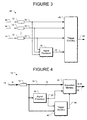
- FIGURE 3 is a block diagram of another test and measurement instrument using a combined signal as a trigger according to an embodiment.
- FIGURE 4 is a block diagram of another test and measurement instrument storing a combined signal and using the combined signal as a trigger according to an embodiment.
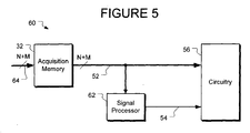
- FIGURE 5 is a block diagram of another test and measurement instrument generating a combined signal from data stored in an acquisition memory according to an embodiment.
- Embodiments include test and measurement instruments and techniques where digitized signals can be combined into a combined signal.
- the combined signal can be used substantially similarly to the source digitized signals.
- FIGURE 1 is a block diagram of a test and measurement instrument using combined signals according to an embodiment.
- the test and measurement instrument 10 includes multiple digitizers 12. In this embodiment, three or more digitizers 12 are illustrated. However, in an embodiment, any number of digitizers greater than one can be used.
- Each digitizer 12 is configured to digitize an input signal 14 to generate a corresponding digitized signal 16.
- the input signal 14 can be any kind of signal that can be digitized.
- the input signal 14 can be a voltage, a current, a temperature, a pressure, or any other parameter.
- the input signal 14 can be a different type of signal representing such parameters.
- a voltage can represent a current converted by a transducer.
- the digitizer 12 can be an appropriate digitizer to digitize such a signal.
- the digitizer 12 can be an analog-to-digital converter (ADC) with a multi-bit output.
- ADC analog-to-digital converter
- Such an ADC can have a voltage input, a current input, or the like.
- the digitizer 12 can be a comparator configured to provide a one-bit output.
- the test and measurement instrument 10 includes a signal processor 18.
- the signal processor 18 is configured to combine at least two of the digitized signals 16 from the digitizers into a combined signal 20.
- the signal processor 18 can be coupled to each of the digitizers 12 and configured to receive each of the digitized signals 16.
- the signal processor can be coupled to the digitizers 12 in different ways.
- the digitized signals 16 that the signal processor 18 is configured to receive can be selected from among the digitized signals 16 through a switch or other routing circuitry. Regardless, the signal processor 18 has access to at least two digitized signals 16.
- the signal processor 18 can be configured to combine the digitized signals 16 in a variety of ways. In one example, the signal processor 18 can be configured to multiply the digitized signals 16 together. If one digitized signal 16 represents a voltage and another digitized signal 16 represents a current, the combined signal 20 can represent a corresponding power. In another example, one digitized signal 16 can be a gating signal that can be used to gate out undesired portions of another digitized signal 16.
- the signal processor 18 can be configured to subtract one digitized signal 16 from another digitized signal 16.
- the combined signal 20 can represent a differential signal.
- the signal processor 18 can be configured to add one digitized signal 16 to another digitized signal 16, representing a common mode signal.
- any mathematical combination can be used.
- one or more of the digitized signals 16 can be filtered, a digitized signal 16 can be used to modulate or demodulate another digitized signal 16, the digitized signals 16 can be combined using linear or non-linear techniques, or the like.
- the signal processor 18 can be configured to combine multiple digitized signals 16 into the combined signal 20 as desired.
- the signal processor 18 can be any variety of circuitry.
- the signal processor 18 can be a digital signal processor, a programmable gate array, an application specific integrated circuit, a discrete logic circuit, a combination of such circuitry, or the like.
- the signal processor 18 can be configured to combine at least two of the digitized signals 16 into the combined signal 20 substantially simultaneously with the digitization of the corresponding input signals 14. That is, as the digitized data of a digitized signal 16 is output from the corresponding digitizer 12, the digitized data can be input into the signal processor 18. Using the example of multiplication to measure a power, one digitizer 12 can output a value indicating an instantaneous voltage. Another digitizer 12 can output a value indicating a corresponding instantaneous current. When these two values are multiplied in the signal processor 18, the output value of the combined signal 20 is the instantaneous power.
- a propagation delay through the signal processor 18 can offset the combined signal 20 in time from the source digitized signals 16, the circuitry 22 can be configured to accommodate such a delay.
- a delay can be introduced into the digitized signal 16 such that the digitized signals 16 and the combined signal 20 are aligned in time.
- the test and measurement instrument 10 can include a delay circuit 24.
- the delay circuit 24 can be configured to time-align the digitized signals 16 and the combined signal 20. Thus, when the signals are incident on the circuitry 22, the signals can be substantially time-aligned.
- the delay circuit 24 is illustrated as operating on the digitized signals 16, the delay circuit can include portions of the signal processor 18, a combination of such circuits, or the like. Any circuit that can introduce a relative time offset between the digitized signals 16 and the combined signal 20 can be used as a delay circuit 24.
- the processing of the signal processor 18 is not performed in a post-processing fashion. That is, the combined signal 20 can be generated at substantially the same time, rather than being generated after full sets of the digitized signals 16 are acquired.
- the combined signal 20 can be used by the circuitry 22 in a manner as if the combined signal 20 was a digitized signal 16 occurring at substantially the same time.
- the circuitry 22 can be any variety of circuitry that can process the digitized signals 16. As will be described in further detail below, the circuitry 22 can be configured to use the combined signal 20 just as the other digitized signals 16 could be used. In particular, a selection can be made from among the digitized signals 16 and the combined signal 20 in association with an acquisition.
- the test and measurement instrument 10 can include means for digitizing a plurality of input signals into a plurality of digitized signals; means for combining at least two of the digitized signals into a combined signal; and means for acquiring data in response to the combined signal.
- the means for digitizing the input signals into the digitized signals 16 can include any variety of the digitizers 12 described above.
- the means for combining at least two of the digitized signals into a combined signal 20 can include any variety of the signal processor 18 described above.
- the means for acquiring data in response to the combined signal 20 can include trigger circuitry, acquisition memories, signal conditioning circuitry, associated controllers, or any other circuit used in acquiring data such as the circuitry 22, described above.
- the digitizers 12 can be configured to substantially continuously digitize the input signals 14. Accordingly, the digitized signals 16 can be substantially continuously presented to the circuitry 22. Similarly, the signal processor 18 can be configured to substantially continuously combine the desired digitized signals 16. Thus, the combined signal 20 can also be substantially continuously presented to the circuitry 22.
- the circuitry 22 can use any of the digitized signals 16 and the combined single 20 as a substantially continuous signal.
- FIGURE 2 is a block diagram of another test and measurement instrument storing a combined signal in an acquisition memory according to an embodiment.
- the test and measurement instrument 30 includes an acquisition memory 32 as part of the circuitry 22. That is, the acquisition memory 32 can be configured to receive the digitized signals 16 and the combined signal 20.
- acquisition memory 32 is memory that is configured to buffer incoming digitized data.
- the acquisition memory 32 can be configured as a circular buffer where new values overwrite older values.
- a window of data can be stored in the acquisition memory 32.
- a window of data of the digitized signals and the combined signal can be stored.
- the stored data can be read out as illustrated by data 34.
- the combined signal 20 can be treated as any other signal to be acquired.
- a trigger can be received.
- the storing of the digitized signals 16 and the combined signal 20 in the acquisition memory 32 can be stopped, the storing can continue for a particular time, or the like.
- the acquisition memory 32 can be any variety of memory.
- the acquisition memory can be dynamic memory, static memory, volatile or non volatile memory, mass-storage device, or the like.
- the acquisition memory can be dynamic memory, static memory, volatile or non volatile memory, mass-storage device, or the like.
- any number of memories can be used.
- each digitized signal 16 and each combined signal 20 can have a dedicated acquisition memory 32.
- the test and measurement instrument 30 can include means for storing the combined signal 20 and at least one of the digitized signals 16.
- the means for storing can include any variety of the acquisition memory 32 described above.
- FIGURE 3 is a block diagram of another test and measurement instrument using a combined signal as a trigger according to an embodiment.
- the test and measurement instrument 40 includes a trigger circuit 42.
- the trigger circuit 42 is configured to trigger an acquisition in response to at least one of the combined signal 20 and/or at least one of the digitized signals 16.
- the trigger circuit 42 can be configured to receive the combined signal 20 and one or more of the digitized signals 16.
- One or more of such signals can be used to trigger an acquisition.
- the combined signal 20 alone can be used to trigger an acquisition.
- a digitized signal 16 can be used to trigger an acquisition.
- the combined signal 20 can be used with one or more digital signals 16 to trigger an acquisition.
- the combined signal 20 can represent a variety of other signals, such as power, a differential signal, a common mode signal, or the like.
- the trigger circuit 42 can generate a trigger signal 44 in response to such signals.
- an acquisition can be triggered in response to a change in power.
- an acquisition can be triggered in response to a signal that can have a different type, character, response, or the like as compared with one of the digitized signals 16.
- the trigger circuit 42 can be any variety of circuit that can generate a trigger signal in response to a digitized signal such as the digitized signals 16 and the combined signal 20.
- the trigger circuit 42 can be a digital signal processor, a programmable gate array, an application specific integrated circuit, a discrete logic circuit, a combination of such circuitry, or the like.
- the test and measurement instrument 40 can include means for triggering an acquisition in response to the combined signal.
- the test and measurement instrument 40 can include means for triggering the acquisition in response to the combined signal and at least one of the digitized signals.
- Such means for triggering can include any variety of the trigger circuit 42 described above.
- FIGURE 4 is a block diagram of another test and measurement instrument storing a combined signal and using the combined signal as a trigger according to an embodiment.
- the test and measurement instrument 50 includes both an acquisition memory 32 and a trigger circuit 42.
- both the acquisition memory 32 and the trigger circuit 42 are configured to receive the combined signal 20.
- the multiple digitizers 12, input signals 14, and digitized signals 16 are combined, illustrating N such elements.
- the acquisition memory 32 can be configured to respond to the trigger signal 44 from the trigger circuit 42.
- an acquisition can be triggered in the acquisition memory 32 of the combined signal 20 in response to a trigger signal 44 generated in response to the combined signal 20.
- the acquisition memory 32 can be configured to store both the digitized signals 16 and the combined signal 20. Accordingly, any or all of such signals can be output as acquired signals 52. Moreover, one combined signal 20 has been used as an example; however, any number M combined signals 20 can be input to the acquisition memory from one or more signal processors 18. Accordingly, N+M acquired signals 52 can be output from the acquisition memory 32.
- the combined signal 20 can be available at substantially the same time as the original digitized signals 16, the combined signal 20 can be used for any purpose as a digitized signal 16.
- FIGURE 5 is a block diagram of another test and measurement instrument generating a combined signal from data stored in an acquisition memory according to an embodiment.
- the test and measurement instrument 60 can include another signal processor 62 similar to the signal processor 18 described above.
- the signal processor 62 is configured to combine acquired signals 52 from the acquisition memory 32. That is, both the acquired signals 52 and another combined signal 54 can be substantially simultaneously presented to and subsequent processing 56.
- the N+M acquired signals 52 can be received by the signal processor 62. That is, not only can the N digitized signals 16 stored in the acquisition memory 32 be combined, but the M combined signals. 20 can be combined in the signal processor 62.
- the acquisition memory 32 need not be configured to store a combined signal 20 as described above. That is, in an embodiment, the signal processor 62 can be the first signal processor capable of combining the digitized signals together encountered by the digitized signals. However, as the signal processor 62 can be configured to combine the digitized signals 52 substantially simultaneously as the digitized signals 52 are output from the acquisition memory 32, the combined signal 54 can be subsequently used as a digitized signal 52.
- a test and measurement instrument can include both such signal processors 18 and 62.
- the signal processor 18 can be configured to generate the combined signal 20 for any use of a digitized signal 16 prior to the acquisition memory 32. If the combined signal 20 is not stored in the acquisition memory 32, additional memory can be available for other acquired signals.
- the signal processor 62 can be configured to create the second combined signal 54 from the signal stored in the acquisition memory.
- the combined signal 54 can be substantially identical to the combined signal 20 generated by the signal processor 18; however, in other embodiments, the combined signal 54 can be different.
Landscapes
- Physics & Mathematics (AREA)
- General Physics & Mathematics (AREA)
- Testing Or Calibration Of Command Recording Devices (AREA)
- Measurement Of Current Or Voltage (AREA)
- Tests Of Electronic Circuits (AREA)
Abstract
Description
- This disclosure relates to test and measurement instruments, in particular to test and measurement instruments using combined signals.
- Test and measurement instruments, such as oscilloscopes, logic analyzers, or the like, can acquire data by digitizing input signals. Such input signals can represent voltages, currents, temperatures, pressures, etc. The digitized input signals can be stored in an acquisition memory. Once an acquisition is triggered, the data can be read out of the acquisition memory as acquired data.
- Such acquired data can be further processed using various waveform math functions. For example, one waveform can be subtracted from another. However, such waveform math is performed entirely after the data has been acquired, transferred among different memories, or the like.
- An embodiment includes a test and measurement instrument including a plurality of digitizers, each digitizer configured to digitize an input signal to generate a digitized signal; a signal processor configured to combine at least two of the digitized signals from the digitizers into a combined signal; and a circuit configured to receive the combined signal and at least one of the digitized signals.
- Another embodiment includes a method including digitizing a plurality of input signals into a plurality of digitized signals; combining at least two of the digitized signals into a combined signal; and selecting from among the digitized signals and the combined signal in association with an acquisition.
-
FIGURE 1 is a block diagram of a test and measurement instrument using combined signals according to an embodiment. -
FIGURE 2 is a block diagram of another test and measurement instrument storing a combined signal in an acquisition memory according to an embodiment. -
FIGURE 3 is a block diagram of another test and measurement instrument using a combined signal as a trigger according to an embodiment. -
FIGURE 4 is a block diagram of another test and measurement instrument storing a combined signal and using the combined signal as a trigger according to an embodiment. -
FIGURE 5 is a block diagram of another test and measurement instrument generating a combined signal from data stored in an acquisition memory according to an embodiment. - Embodiments include test and measurement instruments and techniques where digitized signals can be combined into a combined signal. In an embodiment, the combined signal can be used substantially similarly to the source digitized signals.
-
FIGURE 1 is a block diagram of a test and measurement instrument using combined signals according to an embodiment. In this embodiment, the test andmeasurement instrument 10 includesmultiple digitizers 12. In this embodiment, three ormore digitizers 12 are illustrated. However, in an embodiment, any number of digitizers greater than one can be used. - Each
digitizer 12 is configured to digitize aninput signal 14 to generate a correspondingdigitized signal 16. For example, theinput signal 14 can be any kind of signal that can be digitized. For example, theinput signal 14 can be a voltage, a current, a temperature, a pressure, or any other parameter. In addition, theinput signal 14 can be a different type of signal representing such parameters. For example, a voltage can represent a current converted by a transducer. Regardless, thedigitizer 12 can be an appropriate digitizer to digitize such a signal. For example, thedigitizer 12 can be an analog-to-digital converter (ADC) with a multi-bit output. Such an ADC can have a voltage input, a current input, or the like. In another example, thedigitizer 12 can be a comparator configured to provide a one-bit output. - The test and
measurement instrument 10 includes asignal processor 18. Thesignal processor 18 is configured to combine at least two of thedigitized signals 16 from the digitizers into a combinedsignal 20. For example, thesignal processor 18 can be coupled to each of thedigitizers 12 and configured to receive each of thedigitized signals 16. However, in another embodiment, the signal processor can be coupled to thedigitizers 12 in different ways. For example, thedigitized signals 16 that thesignal processor 18 is configured to receive can be selected from among thedigitized signals 16 through a switch or other routing circuitry. Regardless, thesignal processor 18 has access to at least twodigitized signals 16. - The
signal processor 18 can be configured to combine thedigitized signals 16 in a variety of ways. In one example, thesignal processor 18 can be configured to multiply thedigitized signals 16 together. If onedigitized signal 16 represents a voltage and anotherdigitized signal 16 represents a current, the combinedsignal 20 can represent a corresponding power. In another example, one digitizedsignal 16 can be a gating signal that can be used to gate out undesired portions of another digitizedsignal 16. - In another example, the
signal processor 18 can be configured to subtract onedigitized signal 16 from another digitizedsignal 16. Thus, the combinedsignal 20 can represent a differential signal. Similarly, thesignal processor 18 can be configured to add one digitizedsignal 16 to another digitizedsignal 16, representing a common mode signal. - Moreover, although operations such as multiplication, addition, and subtraction have been described, any mathematical combination can be used. For example, one or more of the
digitized signals 16 can be filtered, a digitizedsignal 16 can be used to modulate or demodulate another digitizedsignal 16, thedigitized signals 16 can be combined using linear or non-linear techniques, or the like. Thus, thesignal processor 18 can be configured to combine multipledigitized signals 16 into the combinedsignal 20 as desired. - The
signal processor 18 can be any variety of circuitry. For example, thesignal processor 18 can be a digital signal processor, a programmable gate array, an application specific integrated circuit, a discrete logic circuit, a combination of such circuitry, or the like. - In an embodiment, the
signal processor 18 can be configured to combine at least two of thedigitized signals 16 into the combinedsignal 20 substantially simultaneously with the digitization of thecorresponding input signals 14. That is, as the digitized data of a digitizedsignal 16 is output from thecorresponding digitizer 12, the digitized data can be input into thesignal processor 18. Using the example of multiplication to measure a power, onedigitizer 12 can output a value indicating an instantaneous voltage. Anotherdigitizer 12 can output a value indicating a corresponding instantaneous current. When these two values are multiplied in thesignal processor 18, the output value of the combinedsignal 20 is the instantaneous power. Although a propagation delay through thesignal processor 18 can offset the combinedsignal 20 in time from the sourcedigitized signals 16, thecircuitry 22 can be configured to accommodate such a delay. For example, a delay can be introduced into the digitizedsignal 16 such that thedigitized signals 16 and the combinedsignal 20 are aligned in time. - In an embodiment, the test and
measurement instrument 10 can include a delay circuit 24. The delay circuit 24 can be configured to time-align thedigitized signals 16 and the combinedsignal 20. Thus, when the signals are incident on thecircuitry 22, the signals can be substantially time-aligned. - Although the delay circuit 24 is illustrated as operating on the
digitized signals 16, the delay circuit can include portions of thesignal processor 18, a combination of such circuits, or the like. Any circuit that can introduce a relative time offset between thedigitized signals 16 and the combinedsignal 20 can be used as a delay circuit 24. - In an embodiment, the processing of the
signal processor 18 is not performed in a post-processing fashion. That is, the combinedsignal 20 can be generated at substantially the same time, rather than being generated after full sets of the digitized signals 16 are acquired. The combinedsignal 20 can be used by thecircuitry 22 in a manner as if the combinedsignal 20 was adigitized signal 16 occurring at substantially the same time. - In an embodiment, the
circuitry 22 can be any variety of circuitry that can process the digitized signals 16. As will be described in further detail below, thecircuitry 22 can be configured to use the combinedsignal 20 just as the otherdigitized signals 16 could be used. In particular, a selection can be made from among the digitized signals 16 and the combinedsignal 20 in association with an acquisition. - In an embodiment, the test and
measurement instrument 10 can include means for digitizing a plurality of input signals into a plurality of digitized signals; means for combining at least two of the digitized signals into a combined signal; and means for acquiring data in response to the combined signal. - The means for digitizing the input signals into the digitized signals 16 can include any variety of the
digitizers 12 described above. The means for combining at least two of the digitized signals into a combinedsignal 20 can include any variety of thesignal processor 18 described above. The means for acquiring data in response to the combinedsignal 20 can include trigger circuitry, acquisition memories, signal conditioning circuitry, associated controllers, or any other circuit used in acquiring data such as thecircuitry 22, described above. - In an embodiment, the
digitizers 12 can be configured to substantially continuously digitize the input signals 14. Accordingly, the digitized signals 16 can be substantially continuously presented to thecircuitry 22. Similarly, thesignal processor 18 can be configured to substantially continuously combine the desired digitized signals 16. Thus, the combinedsignal 20 can also be substantially continuously presented to thecircuitry 22. Thecircuitry 22 can use any of the digitized signals 16 and the combined single 20 as a substantially continuous signal. -
FIGURE 2 is a block diagram of another test and measurement instrument storing a combined signal in an acquisition memory according to an embodiment. In this embodiment, the test andmeasurement instrument 30 includes anacquisition memory 32 as part of thecircuitry 22. That is, theacquisition memory 32 can be configured to receive the digitized signals 16 and the combinedsignal 20. - As used herein,
acquisition memory 32 is memory that is configured to buffer incoming digitized data. For example, theacquisition memory 32 can be configured as a circular buffer where new values overwrite older values. Thus, a window of data can be stored in theacquisition memory 32. In particular, a window of data of the digitized signals and the combined signal can be stored. - Accordingly, when a trigger is generated, or data is otherwise to be acquired, the stored data can be read out as illustrated by
data 34. In particular, the combinedsignal 20 can be treated as any other signal to be acquired. For example, in an embodiment, a trigger can be received. In response, the storing of the digitized signals 16 and the combinedsignal 20 in theacquisition memory 32 can be stopped, the storing can continue for a particular time, or the like. - The
acquisition memory 32 can be any variety of memory. For example, the acquisition memory can be dynamic memory, static memory, volatile or non volatile memory, mass-storage device, or the like. Moreover, although a single memory has been illustrated, any number of memories can be used. For example eachdigitized signal 16 and each combinedsignal 20 can have a dedicatedacquisition memory 32. - In an embodiment, the test and
measurement instrument 30 can include means for storing the combinedsignal 20 and at least one of the digitized signals 16. The means for storing can include any variety of theacquisition memory 32 described above. -
FIGURE 3 is a block diagram of another test and measurement instrument using a combined signal as a trigger according to an embodiment. In this embodiment, the test andmeasurement instrument 40 includes atrigger circuit 42. Thetrigger circuit 42 is configured to trigger an acquisition in response to at least one of the combinedsignal 20 and/or at least one of the digitized signals 16. - That is, the
trigger circuit 42 can be configured to receive the combinedsignal 20 and one or more of the digitized signals 16. One or more of such signals can be used to trigger an acquisition. For example, in the combinedsignal 20 alone can be used to trigger an acquisition. In another example, adigitized signal 16 can be used to trigger an acquisition. In yet another example, the combinedsignal 20 can be used with one or moredigital signals 16 to trigger an acquisition. - In particular, as described above, the combined
signal 20 can represent a variety of other signals, such as power, a differential signal, a common mode signal, or the like. As the combinedsignal 20 representing such signals is presented to thetrigger circuit 42, thetrigger circuit 42 can generate atrigger signal 44 in response to such signals. For example, an acquisition can be triggered in response to a change in power. Thus, an acquisition can be triggered in response to a signal that can have a different type, character, response, or the like as compared with one of the digitized signals 16. - The
trigger circuit 42 can be any variety of circuit that can generate a trigger signal in response to a digitized signal such as the digitized signals 16 and the combinedsignal 20. For example, thetrigger circuit 42 can be a digital signal processor, a programmable gate array, an application specific integrated circuit, a discrete logic circuit, a combination of such circuitry, or the like. - In an embodiment, the test and
measurement instrument 40 can include means for triggering an acquisition in response to the combined signal. In particular, the test andmeasurement instrument 40 can include means for triggering the acquisition in response to the combined signal and at least one of the digitized signals. Such means for triggering can include any variety of thetrigger circuit 42 described above. -
FIGURE 4 is a block diagram of another test and measurement instrument storing a combined signal and using the combined signal as a trigger according to an embodiment. In this embodiment, the test andmeasurement instrument 50 includes both anacquisition memory 32 and atrigger circuit 42. In particular, both theacquisition memory 32 and thetrigger circuit 42 are configured to receive the combinedsignal 20. In this embodiment, for clarity, themultiple digitizers 12, input signals 14, anddigitized signals 16 are combined, illustrating N such elements. - The
acquisition memory 32 can be configured to respond to thetrigger signal 44 from thetrigger circuit 42. In particular, an acquisition can be triggered in theacquisition memory 32 of the combinedsignal 20 in response to atrigger signal 44 generated in response to the combinedsignal 20. - The
acquisition memory 32 can be configured to store both the digitized signals 16 and the combinedsignal 20. Accordingly, any or all of such signals can be output as acquired signals 52. Moreover, one combinedsignal 20 has been used as an example; however, any number M combined signals 20 can be input to the acquisition memory from one ormore signal processors 18. Accordingly, N+M acquired signals 52 can be output from theacquisition memory 32. - Although triggering and storing of a combined
signal 20 in anacquisition memory 32 have been described above, as the combinedsignal 20 can be available at substantially the same time as the originaldigitized signals 16, the combinedsignal 20 can be used for any purpose as adigitized signal 16. -
FIGURE 5 is a block diagram of another test and measurement instrument generating a combined signal from data stored in an acquisition memory according to an embodiment. In this embodiment, the test andmeasurement instrument 60 can include anothersignal processor 62 similar to thesignal processor 18 described above. However, thesignal processor 62 is configured to combine acquiredsignals 52 from theacquisition memory 32. That is, both the acquired signals 52 and another combinedsignal 54 can be substantially simultaneously presented to andsubsequent processing 56. - As illustrated, the N+M acquired signals 52 can be received by the
signal processor 62. That is, not only can the N digitized signals 16 stored in theacquisition memory 32 be combined, but the M combined signals. 20 can be combined in thesignal processor 62. - Moreover, in an embodiment, the
acquisition memory 32 need not be configured to store a combinedsignal 20 as described above. That is, in an embodiment, thesignal processor 62 can be the first signal processor capable of combining the digitized signals together encountered by the digitized signals. However, as thesignal processor 62 can be configured to combine the digitized signals 52 substantially simultaneously as the digitized signals 52 are output from theacquisition memory 32, the combinedsignal 54 can be subsequently used as adigitized signal 52. - However, in an embodiment, a test and measurement instrument can include both
such signal processors signal processor 18 can be configured to generate the combinedsignal 20 for any use of adigitized signal 16 prior to theacquisition memory 32. If the combinedsignal 20 is not stored in theacquisition memory 32, additional memory can be available for other acquired signals. Thesignal processor 62 can be configured to create the second combinedsignal 54 from the signal stored in the acquisition memory. In an embodiment, the combinedsignal 54 can be substantially identical to the combinedsignal 20 generated by thesignal processor 18; however, in other embodiments, the combinedsignal 54 can be different. - Although particular embodiments have been described, it will be appreciated that the principles of the invention are not limited to those embodiments. Variations and modifications may be made without departing from the principles of the invention as set forth in the following claims.
Claims (15)
- A test and measurement instrument, comprising:a plurality of digitizers, each digitizer configured to digitize an input signal to generate a digitized signal;a signal processor configured to combine at least two of the digitized signals from the digitizers into a combined signal; anda circuit configured to receive the combined signal.
- The test and measurement instrument of claim 1, wherein the circuit is further configured to receive at least one of the digitized signals
- The test and measurement instrument of claim 1, further comprising:an acquisition memory configured to store the combined signal.
- The test and measurement instrument of claim 3, wherein the acquisition memory is further configured to store the digitized signals.
- The test and measurement instrument of claim 4, the combined signal referred to as a first combined signal, the test and measurement instrument further comprising:a second signal processor configured to combine at least two signals of the digitized signals and the first combined signal stored in the acquisition memory into a second combined signal and provide the second combined signal as a signal from the acquisition memory.
- The test and measurement instrument of claim 1, further comprising:a trigger circuit configured to trigger an acquisition in response to the combined signal.
- The test and measurement instrument of claim 6, further comprising:an acquisition memory configured to store the combined signal and at least one of the digitized signals.
- The test and measurement instrument of claim 1, wherein the signal processor is configured to combine at least two of the digitized signals into the combined signal substantially simultaneously with the digitization of the corresponding input signals.
- The test and measurement instrument of claim 1, further comprising:a delay circuit configured to substantially time-align the digitized signals and the combined signal;wherein the circuit is configured to receive the time-aligned combined signal and at least one of the digitized signals.
- A method, comprising:digitizing a plurality of input signals into a plurality of digitized signals;combining at least two of the digitized signals into a combined signal; andselecting from among the digitized signals and the combined signal in association with an acquisition.
- The method of claim 10, further comprising:triggering an acquisition in response to the combined signal.
- The method of claim 10, further comprising:storing the combined signal in an acquisition memory.
- The method of claim 10, further comprising:substantially continuously digitizing the input signals.
- The method of claim 10, wherein the digitizing of the input signals and the combining of the at least two digitized signals occurs substantially simultaneously.
- The method of claim 10, further comprising:time-aligning the digitized signals and the combined signal prior to selecting from among the digitized signals and the combined signal.
Applications Claiming Priority (1)
| Application Number | Priority Date | Filing Date | Title |
|---|---|---|---|
| US12/564,800 US10107649B2 (en) | 2009-09-22 | 2009-09-22 | Test and measurement instrument using combined signals |
Publications (2)
| Publication Number | Publication Date |
|---|---|
| EP2299246A1 true EP2299246A1 (en) | 2011-03-23 |
| EP2299246B1 EP2299246B1 (en) | 2016-11-09 |
Family
ID=43479655
Family Applications (1)
| Application Number | Title | Priority Date | Filing Date |
|---|---|---|---|
| EP10251570.7A Active EP2299246B1 (en) | 2009-09-22 | 2010-09-10 | Test and measurement instrument using combined signals |
Country Status (5)
| Country | Link |
|---|---|
| US (1) | US10107649B2 (en) |
| EP (1) | EP2299246B1 (en) |
| JP (1) | JP5605834B2 (en) |
| KR (1) | KR101769868B1 (en) |
| CN (1) | CN102052938B (en) |
Families Citing this family (6)
| Publication number | Priority date | Publication date | Assignee | Title |
|---|---|---|---|---|
| US9568503B2 (en) | 2011-05-26 | 2017-02-14 | Tektronix, Inc. | Calibration for test and measurement instrument including asynchronous time-interleaved digitizer using harmonic mixing |
| US8742749B2 (en) * | 2011-05-26 | 2014-06-03 | Tektronix, Inc. | Test and measurement instrument including asynchronous time-interleaved digitizer using harmonic mixing |
| CN104950152B (en) * | 2014-03-28 | 2020-03-13 | 特克特朗尼克公司 | Test and measurement instrument including asynchronous time interleaved digitizer using harmonic mixing |
| USD947693S1 (en) | 2019-09-20 | 2022-04-05 | Tektronix, Inc. | Measurement probe head assembly |
| JP2022012905A (en) * | 2020-07-02 | 2022-01-17 | キオクシア株式会社 | Memory system and method for managing property information of semiconductor device |
| US11428791B1 (en) * | 2021-10-14 | 2022-08-30 | Motional Ad Llc | Dual-mode silicon photomultiplier based LiDAR |
Citations (2)
| Publication number | Priority date | Publication date | Assignee | Title |
|---|---|---|---|---|
| US20050249037A1 (en) * | 2004-04-28 | 2005-11-10 | Kohn Daniel W | Wireless instrument for the remote monitoring of biological parameters and methods thereof |
| US20080284410A1 (en) * | 2007-05-16 | 2008-11-20 | Square D Company | Clamp-on current and voltage module for a power monitoring system |
Family Cites Families (15)
| Publication number | Priority date | Publication date | Assignee | Title |
|---|---|---|---|---|
| US4768208A (en) * | 1987-03-09 | 1988-08-30 | Motorola, Inc. | Mid-symbol sampling timing estimator |
| JPH029950U (en) * | 1988-07-05 | 1990-01-23 | ||
| JP3088176B2 (en) | 1992-01-24 | 2000-09-18 | 日置電機株式会社 | Waveform display device for waveform recorder |
| JPH06203677A (en) | 1993-01-06 | 1994-07-22 | Toshiba Corp | Insulation rod |
| US5530454A (en) * | 1994-04-13 | 1996-06-25 | Tektronix, Inc. | Digital oscilloscope architecture for signal monitoring with enhanced duty cycle |
| US6201993B1 (en) * | 1998-12-09 | 2001-03-13 | Medtronic, Inc. | Medical device telemetry receiver having improved noise discrimination |
| JP2002286761A (en) | 2001-03-26 | 2002-10-03 | Yokogawa Electric Corp | Multi-phenomenon digital oscilloscope |
| US6892150B2 (en) * | 2002-05-24 | 2005-05-10 | Tektronix, Inc. | Combined analog and DSP trigger system for a digital storage oscilloscope |
| WO2004038432A2 (en) * | 2002-10-24 | 2004-05-06 | Lecroy Corporation | High bandwidth real time oscilloscope |
| US7398175B2 (en) * | 2002-12-18 | 2008-07-08 | Tektronix, Inc. | Method and apparatus providing multiple channel multiple instrument triggering |
| US7184906B2 (en) * | 2003-06-26 | 2007-02-27 | Agilent Technologies, Inc. | Systems and methods for performing multi-source measurements |
| US7672797B2 (en) * | 2006-07-20 | 2010-03-02 | Ads Llc | Flow measurement in partially filled pipes using pulsed peak velocity doppler |
| US8046183B2 (en) * | 2008-03-04 | 2011-10-25 | Tektronix, Inc. | Pre-trigger and post-trigger acquisition for no dead time acquisition system |
| CN201181323Y (en) * | 2008-03-25 | 2009-01-14 | 东莞理工学院 | a logic analyzer |
| CN100588972C (en) * | 2008-05-05 | 2010-02-10 | 电子科技大学 | Dual Time Base Digital Storage Oscilloscope |
-
2009
- 2009-09-22 US US12/564,800 patent/US10107649B2/en active Active
-
2010
- 2010-09-01 JP JP2010196036A patent/JP5605834B2/en active Active
- 2010-09-10 EP EP10251570.7A patent/EP2299246B1/en active Active
- 2010-09-17 KR KR1020100091839A patent/KR101769868B1/en active Active
- 2010-09-21 CN CN201010295421.3A patent/CN102052938B/en not_active Expired - Fee Related
Patent Citations (2)
| Publication number | Priority date | Publication date | Assignee | Title |
|---|---|---|---|---|
| US20050249037A1 (en) * | 2004-04-28 | 2005-11-10 | Kohn Daniel W | Wireless instrument for the remote monitoring of biological parameters and methods thereof |
| US20080284410A1 (en) * | 2007-05-16 | 2008-11-20 | Square D Company | Clamp-on current and voltage module for a power monitoring system |
Also Published As
| Publication number | Publication date |
|---|---|
| CN102052938A (en) | 2011-05-11 |
| US20110071795A1 (en) | 2011-03-24 |
| EP2299246B1 (en) | 2016-11-09 |
| KR101769868B1 (en) | 2017-08-21 |
| KR20110033060A (en) | 2011-03-30 |
| JP2011069820A (en) | 2011-04-07 |
| US10107649B2 (en) | 2018-10-23 |
| CN102052938B (en) | 2016-01-13 |
| JP5605834B2 (en) | 2014-10-15 |
Similar Documents
| Publication | Publication Date | Title |
|---|---|---|
| US10107649B2 (en) | Test and measurement instrument using combined signals | |
| JP4955432B2 (en) | Waveform display device | |
| US7126515B1 (en) | Selectable real time sample triggering for a plurality of inputs of an analog-to-digital converter | |
| WO2007144789A3 (en) | Instrument and method for measuring partial electrical discharges in an electrical system | |
| JP2007018501A (en) | Apparatus and method for updating data in dual port memory | |
| JP2014077791A (en) | Method of indicating correlation between multiple signals, and test measurement device | |
| KR970022357A (en) | Conversion characteristics test circuit and method of analog digital converter | |
| Ramos et al. | Recent developments on impedance measurements with DSP-based ellipse-fitting algorithms | |
| JPH11312975A (en) | Evaluation device for ad converter | |
| US8575983B1 (en) | Waveform generation circuit for a waveform generator | |
| CN107478883B (en) | A kind of method and apparatus for realizing any N times of equivalent sampling | |
| CN109361389A (en) | A kind of timesharing interleaved analog-digital converter multichannel mismatch error calibration method and system | |
| US10326465B1 (en) | Analog to digital converter device and method for generating testing signal | |
| US10788534B2 (en) | Device for dynamic signal generation and analysis | |
| JP2007232571A (en) | Voltage and other effective value calculation circuit and measuring instrument | |
| EP1132744A2 (en) | Measuring device | |
| US20130154860A1 (en) | Use of logic circuit embedded into comparator for foreground offset cancellation | |
| CN104076178A (en) | Oscilloscope with triggering improvement function | |
| US11791928B2 (en) | Digital data rate enhancement filter, digital data rate reduction filter, and digital oscilloscope | |
| Rubini et al. | Design of high performance system-on-chips using Field Programmable Gate Arrays (FPGA) | |
| US11422160B2 (en) | Measurement system and method for generating a trigger signal for a measurement system | |
| US7423565B2 (en) | Apparatus and method for comparison of a plurality of analog signals with selected signals | |
| US11776524B2 (en) | Electromyography signal detection device | |
| CN115015720B (en) | Partial discharge synchronous signal generation method, device, equipment and medium | |
| JP2006318482A (en) | Apparatus and method for generating complementary cumulative distribution function (CCDF) curves |
Legal Events
| Date | Code | Title | Description |
|---|---|---|---|
| PUAI | Public reference made under article 153(3) epc to a published international application that has entered the european phase |
Free format text: ORIGINAL CODE: 0009012 |
|
| AK | Designated contracting states |
Kind code of ref document: A1 Designated state(s): AL AT BE BG CH CY CZ DE DK EE ES FI FR GB GR HR HU IE IS IT LI LT LU LV MC MK MT NL NO PL PT RO SE SI SK SM TR |
|
| AX | Request for extension of the european patent |
Extension state: BA ME RS |
|
| 17P | Request for examination filed |
Effective date: 20110922 |
|
| RAP1 | Party data changed (applicant data changed or rights of an application transferred) |
Owner name: TEKTRONIX, INC. |
|
| 17Q | First examination report despatched |
Effective date: 20151009 |
|
| GRAP | Despatch of communication of intention to grant a patent |
Free format text: ORIGINAL CODE: EPIDOSNIGR1 |
|
| INTG | Intention to grant announced |
Effective date: 20160530 |
|
| GRAS | Grant fee paid |
Free format text: ORIGINAL CODE: EPIDOSNIGR3 |
|
| GRAA | (expected) grant |
Free format text: ORIGINAL CODE: 0009210 |
|
| AK | Designated contracting states |
Kind code of ref document: B1 Designated state(s): AL AT BE BG CH CY CZ DE DK EE ES FI FR GB GR HR HU IE IS IT LI LT LU LV MC MK MT NL NO PL PT RO SE SI SK SM TR |
|
| REG | Reference to a national code |
Ref country code: GB Ref legal event code: FG4D |
|
| REG | Reference to a national code |
Ref country code: AT Ref legal event code: REF Ref document number: 844359 Country of ref document: AT Kind code of ref document: T Effective date: 20161115 Ref country code: CH Ref legal event code: EP |
|
| REG | Reference to a national code |
Ref country code: IE Ref legal event code: FG4D |
|
| REG | Reference to a national code |
Ref country code: DE Ref legal event code: R096 Ref document number: 602010037798 Country of ref document: DE |
|
| PG25 | Lapsed in a contracting state [announced via postgrant information from national office to epo] |
Ref country code: LV Free format text: LAPSE BECAUSE OF FAILURE TO SUBMIT A TRANSLATION OF THE DESCRIPTION OR TO PAY THE FEE WITHIN THE PRESCRIBED TIME-LIMIT Effective date: 20161109 |
|
| REG | Reference to a national code |
Ref country code: LT Ref legal event code: MG4D |
|
| REG | Reference to a national code |
Ref country code: NL Ref legal event code: MP Effective date: 20161109 |
|
| REG | Reference to a national code |
Ref country code: AT Ref legal event code: MK05 Ref document number: 844359 Country of ref document: AT Kind code of ref document: T Effective date: 20161109 |
|
| PG25 | Lapsed in a contracting state [announced via postgrant information from national office to epo] |
Ref country code: NO Free format text: LAPSE BECAUSE OF FAILURE TO SUBMIT A TRANSLATION OF THE DESCRIPTION OR TO PAY THE FEE WITHIN THE PRESCRIBED TIME-LIMIT Effective date: 20170209 Ref country code: LT Free format text: LAPSE BECAUSE OF FAILURE TO SUBMIT A TRANSLATION OF THE DESCRIPTION OR TO PAY THE FEE WITHIN THE PRESCRIBED TIME-LIMIT Effective date: 20161109 Ref country code: NL Free format text: LAPSE BECAUSE OF FAILURE TO SUBMIT A TRANSLATION OF THE DESCRIPTION OR TO PAY THE FEE WITHIN THE PRESCRIBED TIME-LIMIT Effective date: 20161109 Ref country code: SE Free format text: LAPSE BECAUSE OF FAILURE TO SUBMIT A TRANSLATION OF THE DESCRIPTION OR TO PAY THE FEE WITHIN THE PRESCRIBED TIME-LIMIT Effective date: 20161109 Ref country code: GR Free format text: LAPSE BECAUSE OF FAILURE TO SUBMIT A TRANSLATION OF THE DESCRIPTION OR TO PAY THE FEE WITHIN THE PRESCRIBED TIME-LIMIT Effective date: 20170210 |
|
| PG25 | Lapsed in a contracting state [announced via postgrant information from national office to epo] |
Ref country code: AT Free format text: LAPSE BECAUSE OF FAILURE TO SUBMIT A TRANSLATION OF THE DESCRIPTION OR TO PAY THE FEE WITHIN THE PRESCRIBED TIME-LIMIT Effective date: 20161109 Ref country code: PT Free format text: LAPSE BECAUSE OF FAILURE TO SUBMIT A TRANSLATION OF THE DESCRIPTION OR TO PAY THE FEE WITHIN THE PRESCRIBED TIME-LIMIT Effective date: 20170309 Ref country code: FI Free format text: LAPSE BECAUSE OF FAILURE TO SUBMIT A TRANSLATION OF THE DESCRIPTION OR TO PAY THE FEE WITHIN THE PRESCRIBED TIME-LIMIT Effective date: 20161109 Ref country code: ES Free format text: LAPSE BECAUSE OF FAILURE TO SUBMIT A TRANSLATION OF THE DESCRIPTION OR TO PAY THE FEE WITHIN THE PRESCRIBED TIME-LIMIT Effective date: 20161109 Ref country code: PL Free format text: LAPSE BECAUSE OF FAILURE TO SUBMIT A TRANSLATION OF THE DESCRIPTION OR TO PAY THE FEE WITHIN THE PRESCRIBED TIME-LIMIT Effective date: 20161109 Ref country code: IS Free format text: LAPSE BECAUSE OF FAILURE TO SUBMIT A TRANSLATION OF THE DESCRIPTION OR TO PAY THE FEE WITHIN THE PRESCRIBED TIME-LIMIT Effective date: 20170309 Ref country code: HR Free format text: LAPSE BECAUSE OF FAILURE TO SUBMIT A TRANSLATION OF THE DESCRIPTION OR TO PAY THE FEE WITHIN THE PRESCRIBED TIME-LIMIT Effective date: 20161109 |
|
| PG25 | Lapsed in a contracting state [announced via postgrant information from national office to epo] |
Ref country code: RO Free format text: LAPSE BECAUSE OF FAILURE TO SUBMIT A TRANSLATION OF THE DESCRIPTION OR TO PAY THE FEE WITHIN THE PRESCRIBED TIME-LIMIT Effective date: 20161109 Ref country code: DK Free format text: LAPSE BECAUSE OF FAILURE TO SUBMIT A TRANSLATION OF THE DESCRIPTION OR TO PAY THE FEE WITHIN THE PRESCRIBED TIME-LIMIT Effective date: 20161109 Ref country code: EE Free format text: LAPSE BECAUSE OF FAILURE TO SUBMIT A TRANSLATION OF THE DESCRIPTION OR TO PAY THE FEE WITHIN THE PRESCRIBED TIME-LIMIT Effective date: 20161109 Ref country code: CZ Free format text: LAPSE BECAUSE OF FAILURE TO SUBMIT A TRANSLATION OF THE DESCRIPTION OR TO PAY THE FEE WITHIN THE PRESCRIBED TIME-LIMIT Effective date: 20161109 Ref country code: SK Free format text: LAPSE BECAUSE OF FAILURE TO SUBMIT A TRANSLATION OF THE DESCRIPTION OR TO PAY THE FEE WITHIN THE PRESCRIBED TIME-LIMIT Effective date: 20161109 |
|
| REG | Reference to a national code |
Ref country code: DE Ref legal event code: R097 Ref document number: 602010037798 Country of ref document: DE |
|
| PG25 | Lapsed in a contracting state [announced via postgrant information from national office to epo] |
Ref country code: IT Free format text: LAPSE BECAUSE OF FAILURE TO SUBMIT A TRANSLATION OF THE DESCRIPTION OR TO PAY THE FEE WITHIN THE PRESCRIBED TIME-LIMIT Effective date: 20161109 Ref country code: SM Free format text: LAPSE BECAUSE OF FAILURE TO SUBMIT A TRANSLATION OF THE DESCRIPTION OR TO PAY THE FEE WITHIN THE PRESCRIBED TIME-LIMIT Effective date: 20161109 Ref country code: BG Free format text: LAPSE BECAUSE OF FAILURE TO SUBMIT A TRANSLATION OF THE DESCRIPTION OR TO PAY THE FEE WITHIN THE PRESCRIBED TIME-LIMIT Effective date: 20170209 Ref country code: BE Free format text: LAPSE BECAUSE OF FAILURE TO SUBMIT A TRANSLATION OF THE DESCRIPTION OR TO PAY THE FEE WITHIN THE PRESCRIBED TIME-LIMIT Effective date: 20161109 |
|
| PLBE | No opposition filed within time limit |
Free format text: ORIGINAL CODE: 0009261 |
|
| STAA | Information on the status of an ep patent application or granted ep patent |
Free format text: STATUS: NO OPPOSITION FILED WITHIN TIME LIMIT |
|
| 26N | No opposition filed |
Effective date: 20170810 |
|
| PG25 | Lapsed in a contracting state [announced via postgrant information from national office to epo] |
Ref country code: SI Free format text: LAPSE BECAUSE OF FAILURE TO SUBMIT A TRANSLATION OF THE DESCRIPTION OR TO PAY THE FEE WITHIN THE PRESCRIBED TIME-LIMIT Effective date: 20161109 |
|
| REG | Reference to a national code |
Ref country code: CH Ref legal event code: PL |
|
| PG25 | Lapsed in a contracting state [announced via postgrant information from national office to epo] |
Ref country code: MC Free format text: LAPSE BECAUSE OF FAILURE TO SUBMIT A TRANSLATION OF THE DESCRIPTION OR TO PAY THE FEE WITHIN THE PRESCRIBED TIME-LIMIT Effective date: 20161109 |
|
| REG | Reference to a national code |
Ref country code: IE Ref legal event code: MM4A |
|
| PG25 | Lapsed in a contracting state [announced via postgrant information from national office to epo] |
Ref country code: LU Free format text: LAPSE BECAUSE OF NON-PAYMENT OF DUE FEES Effective date: 20170910 |
|
| REG | Reference to a national code |
Ref country code: FR Ref legal event code: ST Effective date: 20180531 |
|
| PG25 | Lapsed in a contracting state [announced via postgrant information from national office to epo] |
Ref country code: CH Free format text: LAPSE BECAUSE OF NON-PAYMENT OF DUE FEES Effective date: 20170930 Ref country code: IE Free format text: LAPSE BECAUSE OF NON-PAYMENT OF DUE FEES Effective date: 20170910 Ref country code: LI Free format text: LAPSE BECAUSE OF NON-PAYMENT OF DUE FEES Effective date: 20170930 |
|
| PG25 | Lapsed in a contracting state [announced via postgrant information from national office to epo] |
Ref country code: FR Free format text: LAPSE BECAUSE OF NON-PAYMENT OF DUE FEES Effective date: 20171002 |
|
| PG25 | Lapsed in a contracting state [announced via postgrant information from national office to epo] |
Ref country code: MT Free format text: LAPSE BECAUSE OF NON-PAYMENT OF DUE FEES Effective date: 20170910 |
|
| PGFP | Annual fee paid to national office [announced via postgrant information from national office to epo] |
Ref country code: GB Payment date: 20180927 Year of fee payment: 9 |
|
| PG25 | Lapsed in a contracting state [announced via postgrant information from national office to epo] |
Ref country code: HU Free format text: LAPSE BECAUSE OF FAILURE TO SUBMIT A TRANSLATION OF THE DESCRIPTION OR TO PAY THE FEE WITHIN THE PRESCRIBED TIME-LIMIT; INVALID AB INITIO Effective date: 20100910 |
|
| PG25 | Lapsed in a contracting state [announced via postgrant information from national office to epo] |
Ref country code: CY Free format text: LAPSE BECAUSE OF NON-PAYMENT OF DUE FEES Effective date: 20161109 |
|
| PG25 | Lapsed in a contracting state [announced via postgrant information from national office to epo] |
Ref country code: MK Free format text: LAPSE BECAUSE OF FAILURE TO SUBMIT A TRANSLATION OF THE DESCRIPTION OR TO PAY THE FEE WITHIN THE PRESCRIBED TIME-LIMIT Effective date: 20161109 |
|
| PG25 | Lapsed in a contracting state [announced via postgrant information from national office to epo] |
Ref country code: TR Free format text: LAPSE BECAUSE OF FAILURE TO SUBMIT A TRANSLATION OF THE DESCRIPTION OR TO PAY THE FEE WITHIN THE PRESCRIBED TIME-LIMIT Effective date: 20161109 |
|
| PG25 | Lapsed in a contracting state [announced via postgrant information from national office to epo] |
Ref country code: AL Free format text: LAPSE BECAUSE OF FAILURE TO SUBMIT A TRANSLATION OF THE DESCRIPTION OR TO PAY THE FEE WITHIN THE PRESCRIBED TIME-LIMIT Effective date: 20161109 |
|
| GBPC | Gb: european patent ceased through non-payment of renewal fee |
Effective date: 20190910 |
|
| PG25 | Lapsed in a contracting state [announced via postgrant information from national office to epo] |
Ref country code: GB Free format text: LAPSE BECAUSE OF NON-PAYMENT OF DUE FEES Effective date: 20190910 |
|
| P01 | Opt-out of the competence of the unified patent court (upc) registered |
Effective date: 20230530 |
|
| PGFP | Annual fee paid to national office [announced via postgrant information from national office to epo] |
Ref country code: DE Payment date: 20250929 Year of fee payment: 16 |