EP2297813B1 - Electronic device suitable for bioimplantation - Google Patents
Electronic device suitable for bioimplantation Download PDFInfo
- Publication number
- EP2297813B1 EP2297813B1 EP09757924.7A EP09757924A EP2297813B1 EP 2297813 B1 EP2297813 B1 EP 2297813B1 EP 09757924 A EP09757924 A EP 09757924A EP 2297813 B1 EP2297813 B1 EP 2297813B1
- Authority
- EP
- European Patent Office
- Prior art keywords
- electronic device
- power source
- casing
- shape
- stack
- Prior art date
- Legal status (The legal status is an assumption and is not a legal conclusion. Google has not performed a legal analysis and makes no representation as to the accuracy of the status listed.)
- Active
Links
Images
Classifications
-
- H—ELECTRICITY
- H01—ELECTRIC ELEMENTS
- H01M—PROCESSES OR MEANS, e.g. BATTERIES, FOR THE DIRECT CONVERSION OF CHEMICAL ENERGY INTO ELECTRICAL ENERGY
- H01M10/00—Secondary cells; Manufacture thereof
- H01M10/42—Methods or arrangements for servicing or maintenance of secondary cells or secondary half-cells
- H01M10/46—Accumulators structurally combined with charging apparatus
-
- H—ELECTRICITY
- H01—ELECTRIC ELEMENTS
- H01M—PROCESSES OR MEANS, e.g. BATTERIES, FOR THE DIRECT CONVERSION OF CHEMICAL ENERGY INTO ELECTRICAL ENERGY
- H01M10/00—Secondary cells; Manufacture thereof
- H01M10/42—Methods or arrangements for servicing or maintenance of secondary cells or secondary half-cells
- H01M10/425—Structural combination with electronic components, e.g. electronic circuits integrated to the outside of the casing
-
- H—ELECTRICITY
- H01—ELECTRIC ELEMENTS
- H01M—PROCESSES OR MEANS, e.g. BATTERIES, FOR THE DIRECT CONVERSION OF CHEMICAL ENERGY INTO ELECTRICAL ENERGY
- H01M10/00—Secondary cells; Manufacture thereof
- H01M10/42—Methods or arrangements for servicing or maintenance of secondary cells or secondary half-cells
- H01M10/44—Methods for charging or discharging
-
- A—HUMAN NECESSITIES
- A61—MEDICAL OR VETERINARY SCIENCE; HYGIENE
- A61N—ELECTROTHERAPY; MAGNETOTHERAPY; RADIATION THERAPY; ULTRASOUND THERAPY
- A61N1/00—Electrotherapy; Circuits therefor
- A61N1/18—Applying electric currents by contact electrodes
- A61N1/32—Applying electric currents by contact electrodes alternating or intermittent currents
- A61N1/36—Applying electric currents by contact electrodes alternating or intermittent currents for stimulation
- A61N1/372—Arrangements in connection with the implantation of stimulators
- A61N1/378—Electrical supply
- A61N1/3787—Electrical supply from an external energy source
-
- Y—GENERAL TAGGING OF NEW TECHNOLOGICAL DEVELOPMENTS; GENERAL TAGGING OF CROSS-SECTIONAL TECHNOLOGIES SPANNING OVER SEVERAL SECTIONS OF THE IPC; TECHNICAL SUBJECTS COVERED BY FORMER USPC CROSS-REFERENCE ART COLLECTIONS [XRACs] AND DIGESTS
- Y02—TECHNOLOGIES OR APPLICATIONS FOR MITIGATION OR ADAPTATION AGAINST CLIMATE CHANGE
- Y02E—REDUCTION OF GREENHOUSE GAS [GHG] EMISSIONS, RELATED TO ENERGY GENERATION, TRANSMISSION OR DISTRIBUTION
- Y02E60/00—Enabling technologies; Technologies with a potential or indirect contribution to GHG emissions mitigation
- Y02E60/10—Energy storage using batteries
Definitions
- the invention relates to an electronic device suitable for bioimplantation.
- the invention also relates to an assembly of an electronic device according to the invention and a charging unit adapted to generate a magnetic field.
- bioimplantable electronic devices can be wirelessly charged by means of a magnetic field (inductively charged).
- the known bioimplantable electronic device therefore comprises a (re)chargeable power source and a coil connected to said power source to enable wirelessly charging of the power source by means of a magnetic field (inductively charged).
- the amount of energy that can be transferred scales quadratically with the area of the coil used, which means in general that the bulk of the electrical current is generated in the largest windings of the coil.
- the restriction makes the application of a flat (2D) rectangular or circular coil design rather inefficient. Moreover, this restriction implies that a electronic device with a small footprint, which can merely incorporate a small coil, can hardly be recharged.
- US 5,749,909 discloses an energy transmission system for transmitting energy non-invasively from an external unit to an implanted medical device to recharge a battery in the medical device.
- An alternating magnetic field is generated by the external charging unit and a piezoelectric device in the implanted medical device vibrates in response to the magnetic flux to generate a voltage.
- the voltage is rectified and regulated to provide charging current to a rechargeable battery in the medical device.
- US2007/0296283 A1 discloses a power generation device that generates power by subjecting a composite of magnetostrictive material and piezo material to a magnetic field.
- the composite of magnetostrictive material and piezo material may be incorporated in a battery or other storage device.
- an electronic device suitable for bioimplantation comprising: at least one rechargeable power source, at least one electronic component connected to said power source, and magnetoelectric conversion means connected to said power source to enable recharging of said power source, said magnetoelectric conversion means comprising at least one stack stack of at least one magnetoelastic layer and at least one piezoelectric layer, wherein said magnetoelectric conversion means has a three-dimensional geometry for receiving and magnetoelectrically converting a magnetic field originating from multiple directions respectively.
- the magnetoelectric stack is applied to an internal or external surface of a casing of the electronic device, wherein the casing has a substantially spherical pill shape or a substantially cylindrical pill shape, a round pill shape, an ellipsoidal shape, an elongated capsule shape, an elongated ellipsoid shape, a super-elliptical cylindrical shape, or a cardioid cylindrical pill shape.
- the substantially improved efficiency of the electronic device is firstly due to the application of said magnetoelectric stack (laminate) of said at least one magnetoelastic layer and said at least one piezoelectric layer, preferably a stack of at least one piezoelectric layer which is sandwiched between multiple magnetoelastic layers, by means of which stack the magnetic field induced can be converted relatively efficiently into electrical energy.
- said stack is subjected to an (alternating) magnetic field the magnetoelastic layer and consequently the piezoelectric layer will be deformed resulting in the generation of an electrical current within the piezoelectric layer.
- the induced electrical current is subsequently used to (re)charge the power source of the electronic device.
- magnetoelectric thus refers to the effect in which an electric current is produced in a laminate when it is subjected to a magnetic field.
- pieoelectric refers to the effect in those materials which only produce an electric output when they experience a change in mechanical load.
- the substantially improved efficiency of the electronic device according to the invention is secondly due to the improved degree of freedom of design of the magnetoelectric conversion means, and hence of the electronic device as such, which degree of freedom is many times larger than this freedom offered by the state of the art. Due to this freedom of design the magnetoelectric conversion means is easily provided a three-dimensional geometry for receiving and magnetoelectrically converting a magnetic field originating from multiple directions respectively.
- the term "three-dimensional geometry” implies the application of a magnetoelectric stack provided with a three-dimensional shape such that an improved probability can be obtained that at least a part of said stack is oriented substantially perpendicular to (a component of) the applied magnetic field, in order to secure the generation of sufficient electrical energy to charge the power source of the electronic device according to the invention.
- the risk of depletion of all electrical energy that can be provided by the power source due to (too) poor charging of the power source can thus be counteracted this way.
- the electronic device can either be fixedly attached to the body or can, to a certain extent, be freely moveably within said body cavity.
- the electronic device according to the invention will commonly be used as bioimplantable device, it would also be conceivable to apply the electronic device in other applications, for example in water treatment plants or in chemical engineering equipment such as a chemical reactors, pipelines, et cetera.
- Suitable materials to be utilized as the magnetoelastic material in a magnetoelastic sensor may be any material with a non-zero magnetostriction and a high magnetoelastic coupling, such as iron-nickel alloys, rare earth metals, ferrites, such as spinel type ferrites (Fe 3 O 4 , MnFe 2 O 4 ), silicon-iron alloys, many other different alloys and mixtures thereof.
- Soft magnetoelastic materials, alloys and mixtures thereof as well as amorphous magnetoelastic materials, alloys and mixtures thereof may be utilized.
- Examples of amorphous magnetoelastic alloys are metglases such as Fe 40 Ni 38 MO 4 B 18 , e.g.
- Metglas 2826MBTM Honeywell Amorphous Metals, Pittsburg, PA, USA
- (FeCo) 80 B 20 (CoNi) 80 B 20 and (FeNi) 80 B 20 .
- suitable elastomagnetic materials are: Ni 2 MnGa, Ni-Mn-Ga alloys, Ni-Ti alloys, Ag-Cd alloys (44/49 at.% Cd), Au-Cd alloys (46,5/50 at.% Cd), Cu-Al-Ni alloys (14/14.5 wt.% A1 and 3/4.5 wt.% Ni), Cu-Sn alloys (approx.
- the size of the dimensional change depends on the magnetization in the material and, of course, on the material properties.
- the phenomenon of magnetostriction is due to the interaction between the atomic magnetic moments in the material.
- the piezoelectric layer is preferably selected from the group consisting of lead zirconate titanate (PZT), lead zincate niobate (PZN), lead zincate niobate lead-titanate (PZN-PT), lead magnesium niobate lead-titanate (PMN-PT), lead lanthanum zirconate titanate (PLZT), Nb/Ta doped-PLZT, barium zirconate titanate (BZT), lead metanobiate, polyvinylidene fluoride (PVFD), polyvinyl chloride (PVC), quartz, barium titanate, cadmium sulphide, topaz, tourmaline, and cane sugar.
- PVFD polyvinylidene fluoride
- PVC polyvin
- the electronic device preferably comprises a protective casing enclosing the power source and/or the at least one electronic component at least substantially. More preferably, the casing is adapted to shield the power source and/or the electronic component against surrounding fluids, in particular body fluids, to enhance the life span of both the power source and the electronic component.
- the casing can further be adapted to enclose the magnetoelectric conversion means at least substantially, wherein at least a part of the magnetoelectric stack is applied onto an internal surface of said casing. However, according to an alternative aspect of the invention at least a part of the magnetoelectric stack is applied onto an external surface of said casing.
- the magnetoelectric stack may cover an entire surface of said casing.
- the magnetoelectric stack merely covers a casing surface partially, wherein a remaining part of said casing surface is left uncovered.
- Application of the stack onto a casing surface is preferably realised by successive deposition of the stack layers by means of one of the following (known) techniques: chemical vapour deposition (CVD), physical vapour deposition (PVD), atomic layer deposition (ALD), sol-gel (impregnation) techniques, melt casting, die casting, spray coating, or flash evaporation.
- CVD chemical vapour deposition
- PVD physical vapour deposition
- ALD atomic layer deposition
- sol-gel sol-gel
- the casing applied may be either rather rigid or rather flexible depending on the composition and thickness of the casing.
- Application of a relatively flexible casing could be particularly favourable, since external forces applied to the casing will also cause deformation of the piezoelectric layer leading to (additional) charging of the power source.
- the casing has a substantially spherical pill shape or a substantially cylindrical pill shape, which shapes are commonly very well suitable to be incorporated in a human or animal body.
- the invention comprises a casing having a round pill shape, an ellipsoidal shape, an elongated capsule shape, an elongated ellipsoid shape, an elongated rectangular shape, a super elliptical cylindrical shape, a cardioid cylindrical pill shape.
- the power source applied preferably comprises at least one solid-state battery, and more preferably a thin film battery comprising a substrate, and at least one battery stack deposited onto said substrate, the battery stack comprising: a first battery electrode, a second battery electrode, and an intermediate solid-state electrolyte separating the first battery electrode and the second battery electrode.
- at least one battery electrode of the power source is adapted for storage of active species of at least one of following elements: hydrogen (H), lithium (Li), beryllium (Be), magnesium (Mg), aluminium (Al), copper (Cu), silver (Ag), sodium (Na) and potassium (K), or any other suitable element which is assigned to group 1 or group 2 of the periodic table.
- the power source of the electrical device according to the invention may be based on various intercalation mechanisms and is therefore suitable to form different kinds of batteries, e.g. Li-ion batteries, NiMH batteries, et cetera.
- at least one battery electrode more preferably the battery anode, comprises at least one of the following materials: C, Sn, Ge, Pb, Zn, Bi, Sb, Li, and, preferably doped, Si.
- C, Sn, Ge, Pb, Zn, Bi, Sb, Li and, preferably doped, Si.
- n-type or p-type doped Si is used as battery electrode, or a doped Si-related compound, like SiGe or SiGeC.
- the battery anode preferably any other suitable element which is assigned to one of groups 12-16 of the periodic table, provided that the material of the battery electrode is adapted for intercalation and storing of the abovementioned reactive species.
- the aforementioned materials are in particularly suitable to be applied in lithium ion batteries.
- the battery anode preferably comprises a hydride forming material, such as AB 5 -type materials, in particular LaNi 5 , and such as magnesium-based alloys, in particular Mg x Ti 1-x .
- the battery cathode for a lithium ion based energy source preferably comprises at least one metal-oxide based material, e.g.
- the battery cathode preferably comprises Ni(OH) 2 and/or NiM(OH) 2 , wherein M is formed by one or more elements selected from the group of e.g. Cd, Co, or Bi. Further embodiments are disclosed in the international application WO 2008/032252 in the name of applicant.
- the power source may comprise at least one capacitor to power the electronic component of the electronic device according to the invention.
- capacitors can be used among which wet/dry capacitors, elcos, supercaps, ultracaps, et cetera.
- the electrical component comprises at least one component chosen from the following group of components: a sensor, such as a temperature sensor or an acidity sensor, a transmitter, a receiver, a camera, an actuator, and a pump.
- the electronic device commonly comprises a power management system connected to both the power source and the magnetoelectric conversion means.
- the primary function of said power management system is to optimise a relatively quick and safe (re)charging process of the power source dependent on the characteristics of said power source.
- the power management typically comprises an electric convertor (DC-DC or AC-DC) to convert the voltage induced within the magnetoelectric means to a desired voltage for the power source to be charged.
- DC-DC or AC-DC an electric convertor
- the power management system comprises a second converter for converting the voltage of the power source to the voltage requirement by the electric component powered by said power source.
- the (micro)controller preferably also checks the voltage provided to the electric component in order to be able to prevent said voltage to drop below a minimum voltage required by said electric component.
- the invention also relates to an assembly of an electronic device according to the invention and a charging unit adapted to generate a magnetic field, preferably an alternating magnetic field.
- the charging unit commonly comprises one or multiple coils to induce the magnetic field.
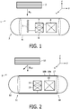
- Fig. 1 shows a schematic cross section of an assembly 1 of a magnetic charging unit 2 and a bioimplantable electronic device 3 known from the prior art.
- the known device 3 comprises a cylindrical pill shaped housing 4 enclosing a coil 5, a power management system 6 connected to said coil 5, a rechargeable battery 7 connected to said power management system 6, and an electronic component 8, such as a sensor, connected to said battery 7.
- an alternating magnetic field B is imposed to the electronic device 3.
- the coil 5 will convert the magnetic field B into electrical energy which is used to (re)charge the battery 7.
- a first drawback of the known device 3 is that by means of the coil 5 merely a relatively poor and inefficient transfer of energy within the device 3 can be achieved.
- the coil 5 is substantially sensitive for a magnetic field B z which is perpendicular to each winding of the coil 5. In case the magnetic field would originate from another direction than the z-direction, this would further deteriorate or even cease the charging process.
- Fig. 2 shows a schematic cross section of an assembly 9 of a magnetic charging unit 10 and a bioimplantable electronic device 11 according to the invention.
- the charging unit 10 commonly comprises one or multiple coils (not shown) to induce a magnetic field B.
- the device 11 according to the invention comprises a cylindrical pill shaped housing 12 enclosing a power management system 13, a rechargeable solid-state battery 14 connected to said power management system 13, and an electronic component 15, such as a sensor, connected to said battery 14.
- An external surface of the housing 12 is partially covered with a magnetoelectric laminate 16 comprising a piezoelectric layer 17 sandwiched in between two magnetoelastic layers 18a, 18b.
- the magnetoelectric laminate 16 is coupled to the power management system 13.
- the magnetoelectric laminate 16 is deposited onto the housing 12 by means of conventional techniques. As shown in this figure the magnetoelectric laminate 16 has a three-dimensional shape as a result of which said laminate 16 is adapted to efficiently convert a magnetic field B originating from the x-direction and/or the z-direction. In case the external surface of the housing 12 would be covered completely by the laminate 16, then laminate 16 would also be adapted to efficiently convert a magnetic field B originating from the y-direction. This makes the orientation of the device 11 with respect to the charging unit 10 less critical, and improves and secures the charging process of the battery 14.
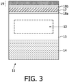
- FIG. 3 An alternative schematic view of the electronic device 11 is shown in figure 3 , wherein the device 11 is shown as a stack of the battery 14, the electrical component 15 incorporating said power management system 13, and the magnetoelectric laminate 16. As also shown in this figure the magnetoelectric laminate 16 is covered by a biocompatible coating 19. Furthermore it is clearly shown in this figure that the piezoelectric layer 17 is enclosed by two magnetoelastic layers 18a, 18b.
Description
- The invention relates to an electronic device suitable for bioimplantation. The invention also relates to an assembly of an electronic device according to the invention and a charging unit adapted to generate a magnetic field.
- During the twentieth century, energy consumption increased dramatically and an unbalanced energy management exists. While there is no sign that this growth in demand will abate (particularly amongst the developing nations), there is now an awareness of the transience of non-renewable resources and the irreversible damage caused to the environment. In addition, there is a trend towards the miniaturization and portability of computing and communications devices. These energy-demanding applications require small, light power sources that are able to sustain operation over long periods of time, particularly in remote locations such as space and exploration. Furthermore, advances in medical science are leading to an increasing number of implantable electrically-operated devices, such as pacemakers and bioimplantable sensors. These devices need power supplies that will operate for extremely long durations as maintenance would necessitate surgery. Presently, bioimplantable electronic devices can be wirelessly charged by means of a magnetic field (inductively charged). The known bioimplantable electronic device therefore comprises a (re)chargeable power source and a coil connected to said power source to enable wirelessly charging of the power source by means of a magnetic field (inductively charged). The amount of energy that can be transferred scales quadratically with the area of the coil used, which means in general that the bulk of the electrical current is generated in the largest windings of the coil. The restriction makes the application of a flat (2D) rectangular or circular coil design rather inefficient. Moreover, this restriction implies that a electronic device with a small footprint, which can merely incorporate a small coil, can hardly be recharged. A further limitation of the known electronic device is that in general the maximum energetic efficiency is obtained when the coil is oriented perpendicular to the applied magnetic field, which is commonly rather hard to achieve in case a implantable device is used which is, to certain extent, freely moveable in a body cavity.
US 5,749,909 discloses an energy transmission system for transmitting energy non-invasively from an external unit to an implanted medical device to recharge a battery in the medical device. An alternating magnetic field is generated by the external charging unit and a piezoelectric device in the implanted medical device vibrates in response to the magnetic flux to generate a voltage. The voltage is rectified and regulated to provide charging current to a rechargeable battery in the medical device.US2007/0296283 A1 discloses a power generation device that generates power by subjecting a composite of magnetostrictive material and piezo material to a magnetic field. The composite of magnetostrictive material and piezo material may be incorporated in a battery or other storage device. - It is an object of the invention to provide a relatively efficient electronic device.
- The object is achieved according to the invention by providing an electronic device suitable for bioimplantation, comprising: at least one rechargeable power source, at least one electronic component connected to said power source, and magnetoelectric conversion means connected to said power source to enable recharging of said power source, said magnetoelectric conversion means comprising at least one stack stack of at least one magnetoelastic layer and at least one piezoelectric layer, wherein said magnetoelectric conversion means has a three-dimensional geometry for receiving and magnetoelectrically converting a magnetic field originating from multiple directions respectively. According to the invention, at least a part of the magnetoelectric stack is applied to an internal or external surface of a casing of the electronic device, wherein the casing has a substantially spherical pill shape or a substantially cylindrical pill shape, a round pill shape, an ellipsoidal shape, an elongated capsule shape, an elongated ellipsoid shape, a super-elliptical cylindrical shape, or a cardioid cylindrical pill shape. The substantially improved efficiency of the electronic device is firstly due to the application of said magnetoelectric stack (laminate) of said at least one magnetoelastic layer and said at least one piezoelectric layer, preferably a stack of at least one piezoelectric layer which is sandwiched between multiple magnetoelastic layers, by means of which stack the magnetic field induced can be converted relatively efficiently into electrical energy. In case said stack is subjected to an (alternating) magnetic field the magnetoelastic layer and consequently the piezoelectric layer will be deformed resulting in the generation of an electrical current within the piezoelectric layer. The induced electrical current is subsequently used to (re)charge the power source of the electronic device. The term "magnetoelectric" thus refers to the effect in which an electric current is produced in a laminate when it is subjected to a magnetic field. The term "piezoelectric" refers to the effect in those materials which only produce an electric output when they experience a change in mechanical load. The substantially improved efficiency of the electronic device according to the invention is secondly due to the improved degree of freedom of design of the magnetoelectric conversion means, and hence of the electronic device as such, which degree of freedom is many times larger than this freedom offered by the state of the art. Due to this freedom of design the magnetoelectric conversion means is easily provided a three-dimensional geometry for receiving and magnetoelectrically converting a magnetic field originating from multiple directions respectively. In this context the term "three-dimensional geometry" implies the application of a magnetoelectric stack provided with a three-dimensional shape such that an improved probability can be obtained that at least a part of said stack is oriented substantially perpendicular to (a component of) the applied magnetic field, in order to secure the generation of sufficient electrical energy to charge the power source of the electronic device according to the invention. The risk of depletion of all electrical energy that can be provided by the power source due to (too) poor charging of the power source can thus be counteracted this way. In case the electronic device is implanted in a body cavity, the electronic device can either be fixedly attached to the body or can, to a certain extent, be freely moveably within said body cavity. Although the electronic device according to the invention will commonly be used as bioimplantable device, it would also be conceivable to apply the electronic device in other applications, for example in water treatment plants or in chemical engineering equipment such as a chemical reactors, pipelines, et cetera.
- Suitable materials to be utilized as the magnetoelastic material in a magnetoelastic sensor may be any material with a non-zero magnetostriction and a high magnetoelastic coupling, such as iron-nickel alloys, rare earth metals, ferrites, such as spinel type ferrites (Fe3O4, MnFe2O4), silicon-iron alloys, many other different alloys and mixtures thereof. Soft magnetoelastic materials, alloys and mixtures thereof as well as amorphous magnetoelastic materials, alloys and mixtures thereof may be utilized. Examples of amorphous magnetoelastic alloys are metglases such as Fe40Ni38MO4B18, e.g. Metglas 2826MB™ (Honeywell Amorphous Metals, Pittsburg, PA, USA), (FeCo)80B20, (CoNi)80B20 and (FeNi)80B20. Other examples of suitable elastomagnetic materials are: Ni2MnGa, Ni-Mn-Ga alloys, Ni-Ti alloys, Ag-Cd alloys (44/49 at.% Cd), Au-Cd alloys (46,5/50 at.% Cd), Cu-Al-Ni alloys (14/14.5 wt.% A1 and 3/4.5 wt.% Ni), Cu-Sn alloys (approx. 15 at.% Sn), Cu-Zn alloys (38.5/41.5 wt.% Zn), Cu-Zn-X alloys wherein X = Si, A1 or Sn; Fe-Pt alloys (approx. 25 at.% Pt), Mn-Cu alloys (5/35 at.% Cu), Fe-Mn-Si, Pt alloys, Co-Ni-Al alloys, Co-Ni-Ga alloys, Ni-Fe-Ga alloys, and Ti-Pd alloys in various concentrations. The term "magnetostriction" introduced in this paragraph refers to a phenomenon whereby a material will change dimensions in the presence of an external magnetic field. The size of the dimensional change depends on the magnetization in the material and, of course, on the material properties. The phenomenon of magnetostriction is due to the interaction between the atomic magnetic moments in the material. The piezoelectric layer is preferably selected from the group consisting of lead zirconate titanate (PZT), lead zincate niobate (PZN), lead zincate niobate lead-titanate (PZN-PT), lead magnesium niobate lead-titanate (PMN-PT), lead lanthanum zirconate titanate (PLZT), Nb/Ta doped-PLZT, barium zirconate titanate (BZT), lead metanobiate, polyvinylidene fluoride (PVFD), polyvinyl chloride (PVC), quartz, barium titanate, cadmium sulphide, topaz, tourmaline, and cane sugar. The electronic device according to the invention preferably comprises a protective casing enclosing the power source and/or the at least one electronic component at least substantially. More preferably, the casing is adapted to shield the power source and/or the electronic component against surrounding fluids, in particular body fluids, to enhance the life span of both the power source and the electronic component. The casing can further be adapted to enclose the magnetoelectric conversion means at least substantially, wherein at least a part of the magnetoelectric stack is applied onto an internal surface of said casing. However, according to an alternative aspect of the invention at least a part of the magnetoelectric stack is applied onto an external surface of said casing. The magnetoelectric stack may cover an entire surface of said casing. However, it is also conceivable that the magnetoelectric stack merely covers a casing surface partially, wherein a remaining part of said casing surface is left uncovered. Application of the stack onto a casing surface is preferably realised by successive deposition of the stack layers by means of one of the following (known) techniques: chemical vapour deposition (CVD), physical vapour deposition (PVD), atomic layer deposition (ALD), sol-gel (impregnation) techniques, melt casting, die casting, spray coating, or flash evaporation. In an alternative preferred embodiment the casing is formed by the magnetoelectric conversion means. By smartly integrating the casing with the magnetoelectric stack a further improved and volume-efficient means of wireless charging is introduced. An additional important advantage is that the overall size of the power source will be smaller as (more efficient) recharging is now possible, resulting in a relatively compact and less-invasive device. The casing applied may be either rather rigid or rather flexible depending on the composition and thickness of the casing. Application of a relatively flexible casing could be particularly favourable, since external forces applied to the casing will also cause deformation of the piezoelectric layer leading to (additional) charging of the power source.
- According to the invention, the casing has a substantially spherical pill shape or a substantially cylindrical pill shape, which shapes are commonly very well suitable to be incorporated in a human or animal body. In addition to these shapes, the invention comprises a casing having a round pill shape, an ellipsoidal shape, an elongated capsule shape, an elongated ellipsoid shape, an elongated rectangular shape, a super elliptical cylindrical shape, a cardioid cylindrical pill shape.
- The power source applied preferably comprises at least one solid-state battery, and more preferably a thin film battery comprising a substrate, and at least one battery stack deposited onto said substrate, the battery stack comprising: a first battery electrode, a second battery electrode, and an intermediate solid-state electrolyte separating the first battery electrode and the second battery electrode. Preferably, at least one battery electrode of the power source is adapted for storage of active species of at least one of following elements: hydrogen (H), lithium (Li), beryllium (Be), magnesium (Mg), aluminium (Al), copper (Cu), silver (Ag), sodium (Na) and potassium (K), or any other suitable element which is assigned to
group 1 orgroup 2 of the periodic table. So, the power source of the electrical device according to the invention may be based on various intercalation mechanisms and is therefore suitable to form different kinds of batteries, e.g. Li-ion batteries, NiMH batteries, et cetera. In a preferred embodiment at least one battery electrode, more preferably the battery anode, comprises at least one of the following materials: C, Sn, Ge, Pb, Zn, Bi, Sb, Li, and, preferably doped, Si. A combination of these materials may also be used to form the battery electrode(s). Preferably, n-type or p-type doped Si is used as battery electrode, or a doped Si-related compound, like SiGe or SiGeC. Also other suitable materials may be applied as battery anode, preferably any other suitable element which is assigned to one of groups 12-16 of the periodic table, provided that the material of the battery electrode is adapted for intercalation and storing of the abovementioned reactive species. The aforementioned materials are in particularly suitable to be applied in lithium ion batteries. In case a hydrogen based energy source is applied, the battery anode preferably comprises a hydride forming material, such as AB5-type materials, in particular LaNi5, and such as magnesium-based alloys, in particular MgxTi1-x. The battery cathode for a lithium ion based energy source preferably comprises at least one metal-oxide based material, e.g. LiCoO2, LiNiO2, LiMnO2 or a combination of these such as. e.g. Li(NiCoMn)O2. In case of a hydrogen based energy source, the battery cathode preferably comprises Ni(OH)2 and/or NiM(OH)2, wherein M is formed by one or more elements selected from the group of e.g. Cd, Co, or Bi. Further embodiments are disclosed in the international applicationWO 2008/032252 in the name of applicant. Alternatively the power source may comprise at least one capacitor to power the electronic component of the electronic device according to the invention. Several types of capacitors can be used among which wet/dry capacitors, elcos, supercaps, ultracaps, et cetera. - In a preferred embodiment the electrical component comprises at least one component chosen from the following group of components: a sensor, such as a temperature sensor or an acidity sensor, a transmitter, a receiver, a camera, an actuator, and a pump. By means of these electronic components a wide range of applications of the electronic device according to the invention can be realised, among which drug delivery devices, neuro-stimulators, (bio)sensors, transmitters, receivers, and/or actuators.
- The electronic device commonly comprises a power management system connected to both the power source and the magnetoelectric conversion means. The primary function of said power management system is to optimise a relatively quick and safe (re)charging process of the power source dependent on the characteristics of said power source. The power management typically comprises an electric convertor (DC-DC or AC-DC) to convert the voltage induced within the magnetoelectric means to a desired voltage for the power source to be charged. By means of a (micro)controller one or multiple charging parameters can be measured, such as the charging current, the charging voltage, and the temperature. Based upon these measurements the charging process can eventually be manipulated and hence further be optimized. Optionally, the power management system comprises a second converter for converting the voltage of the power source to the voltage requirement by the electric component powered by said power source. In case this second converter is applied, the (micro)controller preferably also checks the voltage provided to the electric component in order to be able to prevent said voltage to drop below a minimum voltage required by said electric component.
- The invention also relates to an assembly of an electronic device according to the invention and a charging unit adapted to generate a magnetic field, preferably an alternating magnetic field. The charging unit commonly comprises one or multiple coils to induce the magnetic field.
- The invention is illustrated by way of the following non-limitative examples, wherein:
-
Fig. 1 shows a schematic cross section of an assembly of a magnetic charging unit and a bioimplantable electronic device known from the prior art, -
Fig. 2 shows a schematic cross section of an assembly of a magnetic charging unit and a bioimplantable electronic device according to the invention, and -
Fig. 3 shows an alternative schematic view of the electronic device according tofigure 2 . -
Fig. 1 shows a schematic cross section of anassembly 1 of amagnetic charging unit 2 and a bioimplantableelectronic device 3 known from the prior art. The knowndevice 3 comprises a cylindrical pill shapedhousing 4 enclosing acoil 5, apower management system 6 connected to saidcoil 5, arechargeable battery 7 connected to saidpower management system 6, and anelectronic component 8, such as a sensor, connected to saidbattery 7. By means of the chargingunit 2 an alternating magnetic field B is imposed to theelectronic device 3. Thecoil 5 will convert the magnetic field B into electrical energy which is used to (re)charge thebattery 7. A first drawback of the knowndevice 3 is that by means of thecoil 5 merely a relatively poor and inefficient transfer of energy within thedevice 3 can be achieved. Moreover, thecoil 5 is substantially sensitive for a magnetic field Bz which is perpendicular to each winding of thecoil 5. In case the magnetic field would originate from another direction than the z-direction, this would further deteriorate or even cease the charging process. -
Fig. 2 shows a schematic cross section of anassembly 9 of amagnetic charging unit 10 and a bioimplantableelectronic device 11 according to the invention. The chargingunit 10 commonly comprises one or multiple coils (not shown) to induce a magnetic field B. Thedevice 11 according to the invention comprises a cylindrical pill shapedhousing 12 enclosing apower management system 13, a rechargeable solid-state battery 14 connected to saidpower management system 13, and anelectronic component 15, such as a sensor, connected to saidbattery 14. An external surface of thehousing 12 is partially covered with amagnetoelectric laminate 16 comprising apiezoelectric layer 17 sandwiched in between twomagnetoelastic layers magnetoelectric laminate 16 is coupled to thepower management system 13. Themagnetoelectric laminate 16 is deposited onto thehousing 12 by means of conventional techniques. As shown in this figure themagnetoelectric laminate 16 has a three-dimensional shape as a result of which saidlaminate 16 is adapted to efficiently convert a magnetic field B originating from the x-direction and/or the z-direction. In case the external surface of thehousing 12 would be covered completely by the laminate 16, then laminate 16 would also be adapted to efficiently convert a magnetic field B originating from the y-direction. This makes the orientation of thedevice 11 with respect to the chargingunit 10 less critical, and improves and secures the charging process of thebattery 14. An alternative schematic view of theelectronic device 11 is shown infigure 3 , wherein thedevice 11 is shown as a stack of thebattery 14, theelectrical component 15 incorporating saidpower management system 13, and themagnetoelectric laminate 16. As also shown in this figure themagnetoelectric laminate 16 is covered by abiocompatible coating 19. Furthermore it is clearly shown in this figure that thepiezoelectric layer 17 is enclosed by twomagnetoelastic layers - It should be noted that the above-mentioned embodiments illustrate rather than limit the invention, and that those skilled in the art will be able to design many alternative embodiments. In the claims, any reference signs placed between parentheses shall not be construed as limiting the claim. Use of the verb "comprise" and its conjugations does not exclude the presence of elements or steps other than those stated in a claim. The article "a" or "an" preceding an element does not exclude the presence of a plurality of such elements. The mere fact that certain measures are recited in mutually different dependent claims does not indicate that a combination of these measures cannot be used to advantage.
Claims (14)
- Electronic device (11) suitable for bioimplantation, comprising:- at least one rechargeable power source (14),- at least one electronic component (15) connected to said power source, and- magnetoelectric conversion means connected to said power source to enable recharging of said power source, said magnetoelectric conversion means comprising at least one stack (16) of at least one magnetoelastic layer (18) and at least one piezoelectric layer (17), characterized in that
said at least one stack has a three-dimensional shape such that at least a part of said stack is oriented substantially perpendicular to an applied magnetic field from multiple respective directions for receiving and magnetoelectrically converting the applied magnetic field, at least a part of the magnetoelectric stack being applied onto an internal or external surface of a casing of the electronic device, wherein- the casing has a substantially spherical pill shape or a substantially cylindrical pill shape, or- the casing has a round pill shape, an ellipsoidal shape, an elongated capsule shape, an elongated ellipsoid shape, a super elliptical cylindrical shape, or a cardioid cylindrical pill shape. - Electronic device according to claim 1, wherein the magnetoelectric conversion means comprises a stack of at least one piezoelectric layer (17) which is sandwiched between multiple magnetoelastic layers (18a, 18b)
- Electronic device according to claim 1, wherein the magnetoelastic layer is made of at least one following materials: iron-nickel alloys, rare earth metals, ferrites, in particular spinel type ferrites, and silicon-iron alloys.
- Electronic device according to claim 1, wherein the piezoelectric layer is selected from the group consisting of lead zirconate titanate (PZT), lead zincate niobate (PZN), lead zincate niobate lead-titanate (PZN-PT), lead magnesium niobate lead-titanate (PMN-PT), lead lanthanum zirconate titanate (PLZT), Nb/Ta doped-PLZT, barium zirconate titanate (BZT), lead metanobiate, polyvinylidene fluoride (PVFD), polyvinyl chloride (PVC), quartz, barium titanate, cadmium sulphide, topaz, tourmaline, and cane sugar.
- Electronic device according to claim 1, wherein the casing (12) encloses the power source and/or the electronic component at least substantially.
- Electronic device according to claim 5, wherein the casing further encloses at least a part of the magnetoelectric stack.
- Electronic device according to claim 5, wherein at least a part of the magnetoelectric stack is applied onto the external surface of said casing.
- Electronic device according to claim 5, wherein the casing is formed by the magnetoelectric conversion means.
- Electronic device according to claims 5, wherein the casing has a substantially spherical shape or a substantially cylindrical pill shape.
- Electronic device according to claim 1, wherein the power source comprises at least one solid-state battery.
- Electronic device according to claim 1, wherein the power source comprises at least one capacitor.
- Electronic device according to claim 1, wherein the electrical component comprises at least one component chosen from the following group of components: a sensor, a transmitter, a receiver, a camera, an actuator, and a pump.
- Electronic device according to claim 1, wherein the electronic device comprises a power management system connected to both the power source and the magnetoelectric conversion means.
- Assembly of an electronic device according to claim 1 and a charging unit (10) adapted to generate a magnetic field.
Priority Applications (1)
| Application Number | Priority Date | Filing Date | Title |
|---|---|---|---|
| EP09757924.7A EP2297813B1 (en) | 2008-06-05 | 2009-05-26 | Electronic device suitable for bioimplantation |
Applications Claiming Priority (3)
| Application Number | Priority Date | Filing Date | Title |
|---|---|---|---|
| EP08157658 | 2008-06-05 | ||
| EP09757924.7A EP2297813B1 (en) | 2008-06-05 | 2009-05-26 | Electronic device suitable for bioimplantation |
| PCT/IB2009/052199 WO2009147573A1 (en) | 2008-06-05 | 2009-05-26 | Electronic device suitable for bioimplantation |
Publications (2)
| Publication Number | Publication Date |
|---|---|
| EP2297813A1 EP2297813A1 (en) | 2011-03-23 |
| EP2297813B1 true EP2297813B1 (en) | 2020-09-09 |
Family
ID=40996711
Family Applications (1)
| Application Number | Title | Priority Date | Filing Date |
|---|---|---|---|
| EP09757924.7A Active EP2297813B1 (en) | 2008-06-05 | 2009-05-26 | Electronic device suitable for bioimplantation |
Country Status (5)
| Country | Link |
|---|---|
| US (1) | US8872507B2 (en) |
| EP (1) | EP2297813B1 (en) |
| JP (1) | JP2011525099A (en) |
| CN (1) | CN102057530B (en) |
| WO (1) | WO2009147573A1 (en) |
Families Citing this family (9)
| Publication number | Priority date | Publication date | Assignee | Title |
|---|---|---|---|---|
| AU2013232107B2 (en) * | 2012-03-16 | 2015-11-19 | Boston Scientific Neuromodulation Corporation | Neurostimulation system for preventing magnetically induced currents in electronic circuitry |
| KR102023617B1 (en) * | 2016-03-22 | 2019-09-20 | 삼성전자주식회사 | Method for supplying power to implantable medical device and power supply system thereof |
| CN106253499A (en) * | 2016-08-17 | 2016-12-21 | 桐城市闲产网络服务有限公司 | A kind of novel ultrasound wave Contactless Power Transmission System based on PZT |
| CN106178282A (en) * | 2016-08-31 | 2016-12-07 | 王成章 | Miniature blue light based on external power supply sterilization capsule |
| KR102276765B1 (en) * | 2018-08-30 | 2021-07-12 | 한양대학교 산학협력단 | Capcule endoscope using piezoelectric element |
| US10824822B2 (en) | 2019-02-05 | 2020-11-03 | International Business Machines Corporation | Magnetic tracking for medicine management |
| US10679018B1 (en) * | 2019-02-05 | 2020-06-09 | International Business Machines Corporation | Magnetic tracking for medicine management |
| CN110159758B (en) * | 2019-05-22 | 2020-09-11 | 海信(广东)厨卫系统有限公司 | Pressure container, manufacturing method thereof, pressure container stress detection system and method |
| US11890466B2 (en) * | 2019-07-01 | 2024-02-06 | Wavegate Corporation | IPG and header combination |
Family Cites Families (20)
| Publication number | Priority date | Publication date | Assignee | Title |
|---|---|---|---|---|
| US5749909A (en) * | 1996-11-07 | 1998-05-12 | Sulzer Intermedics Inc. | Transcutaneous energy coupling using piezoelectric device |
| ATE277672T1 (en) * | 1997-08-01 | 2004-10-15 | Mann Alfred E Found Scient Res | IMPLANTABLE DEVICE WITH IMPROVED ARRANGEMENT FOR BATTERY CHARGING AND POWER SUPPLY |
| US6178353B1 (en) * | 1998-07-27 | 2001-01-23 | Advanced Bionics Corporation | Laminated magnet keeper for implant device |
| JP2004528890A (en) * | 2001-04-04 | 2004-09-24 | ギブン・イメージング・リミテッド | Inductive power in vivo imaging device |
| JP3905418B2 (en) * | 2001-05-18 | 2007-04-18 | セイコーインスツル株式会社 | Power supply device and electronic device |
| WO2003037399A2 (en) * | 2001-10-31 | 2003-05-08 | Biophan Technologies, Inc. | Hermetic component housing for photonic catheter |
| US6894456B2 (en) * | 2001-11-07 | 2005-05-17 | Quallion Llc | Implantable medical power module |
| GB2398176B (en) | 2002-05-13 | 2006-03-08 | Zap Wireless Technologies Ltd | Improvements relating to contact-less power transfer |
| US8236443B2 (en) * | 2002-08-09 | 2012-08-07 | Infinite Power Solutions, Inc. | Metal film encapsulation |
| US7023206B2 (en) * | 2002-10-18 | 2006-04-04 | Virginia Tech Intellectual Properties, Inc. | Magnetoelectric magnetic field sensor with longitudinally biased magnetostrictive layer |
| US7808236B1 (en) * | 2002-12-09 | 2010-10-05 | Ferro Solutions, Inc. | Energy harvester utilizing external magnetic field |
| US6984902B1 (en) * | 2003-02-03 | 2006-01-10 | Ferro Solutions, Inc. | High efficiency vibration energy harvester |
| DE10320188A1 (en) | 2003-05-07 | 2004-12-02 | Abb Research Ltd. | Magnetic field generation system |
| JP2006149685A (en) * | 2004-11-29 | 2006-06-15 | Olympus Corp | In-subject introduction device and in-subject introduction system |
| EP2011165A1 (en) | 2006-04-11 | 2009-01-07 | Ferro Solutions, Inc. | Apparatus and method utilizing magnetic field |
| CA2636371C (en) | 2006-04-28 | 2015-06-16 | Cooper Tire & Rubber Company | Long range rfid transponder |
| CA2649880C (en) * | 2006-06-22 | 2015-10-27 | Cooper Tire & Rubber Co. | Magnetostrictive/piezo remote power generation, battery and method |
| US20100167130A1 (en) | 2006-09-14 | 2010-07-01 | Koninklijke Philips Electronics N.V. | Electrochemical energy source and electronic device provided with such an electrochemical energy source |
| US7979126B2 (en) * | 2006-10-18 | 2011-07-12 | Boston Scientific Neuromodulation Corporation | Orientation-independent implantable pulse generator |
| US7573734B2 (en) * | 2007-07-13 | 2009-08-11 | Consejo Superior De Investigaciones Cientificas | Magnetoelectric device and method for writing non-volatile information into said magnetoelectric device |
-
2009
- 2009-05-26 US US12/994,168 patent/US8872507B2/en active Active
- 2009-05-26 JP JP2011512243A patent/JP2011525099A/en active Pending
- 2009-05-26 WO PCT/IB2009/052199 patent/WO2009147573A1/en active Application Filing
- 2009-05-26 CN CN200980120562.7A patent/CN102057530B/en not_active Expired - Fee Related
- 2009-05-26 EP EP09757924.7A patent/EP2297813B1/en active Active
Non-Patent Citations (1)
| Title |
|---|
| None * |
Also Published As
| Publication number | Publication date |
|---|---|
| US8872507B2 (en) | 2014-10-28 |
| EP2297813A1 (en) | 2011-03-23 |
| CN102057530A (en) | 2011-05-11 |
| JP2011525099A (en) | 2011-09-08 |
| US20110101914A1 (en) | 2011-05-05 |
| CN102057530B (en) | 2014-10-29 |
| WO2009147573A1 (en) | 2009-12-10 |
Similar Documents
| Publication | Publication Date | Title |
|---|---|---|
| EP2297813B1 (en) | Electronic device suitable for bioimplantation | |
| KR102418977B1 (en) | Secondary battery and electronic device | |
| US11949061B2 (en) | Secondary battery and electronic device | |
| Rasouli et al. | Energy sources and their development for application in medical devices | |
| US10193108B2 (en) | Secondary battery, electronic device, and vehicle | |
| JP2020198318A (en) | Secondary battery | |
| EP3192163B1 (en) | Flexible, hybrid energy generating and storage power cell | |
| WO2009123672A2 (en) | Electrochemical actuator | |
| US20170164581A1 (en) | Transmitters for Animals and Methods for Transmitting from Animals | |
| EP3567666A1 (en) | Electrode assembly | |
| KR20160055778A (en) | Segmented energy storage assembly | |
| WO2009147587A1 (en) | Wearable rechargeable power system and electronic device | |
| EP3392999B1 (en) | Capsule endoscope | |
| Rebel et al. | Energy harvesting on human bodies | |
| Janicek et al. | Polymer based piezoelectric energy microgenerator | |
| Bilal et al. | Powering the future: Exploring self‐charging cardiac implantable electronic devices and the Qi revolution | |
| JP2010514123A (en) | Electrochemical energy source and electronic device provided with such electrochemical energy source |
Legal Events
| Date | Code | Title | Description |
|---|---|---|---|
| PUAI | Public reference made under article 153(3) epc to a published international application that has entered the european phase |
Free format text: ORIGINAL CODE: 0009012 |
|
| 17P | Request for examination filed |
Effective date: 20110105 |
|
| AK | Designated contracting states |
Kind code of ref document: A1 Designated state(s): AT BE BG CH CY CZ DE DK EE ES FI FR GB GR HR HU IE IS IT LI LT LU LV MC MK MT NL NO PL PT RO SE SI SK TR |
|
| AX | Request for extension of the european patent |
Extension state: AL BA RS |
|
| DAX | Request for extension of the european patent (deleted) | ||
| 17Q | First examination report despatched |
Effective date: 20130225 |
|
| RAP1 | Party data changed (applicant data changed or rights of an application transferred) |
Owner name: KONINKLIJKE PHILIPS N.V. |
|
| STAA | Information on the status of an ep patent application or granted ep patent |
Free format text: STATUS: EXAMINATION IS IN PROGRESS |
|
| RAP1 | Party data changed (applicant data changed or rights of an application transferred) |
Owner name: KONINKLIJKE PHILIPS N.V. |
|
| GRAP | Despatch of communication of intention to grant a patent |
Free format text: ORIGINAL CODE: EPIDOSNIGR1 |
|
| STAA | Information on the status of an ep patent application or granted ep patent |
Free format text: STATUS: GRANT OF PATENT IS INTENDED |
|
| INTG | Intention to grant announced |
Effective date: 20200326 |
|
| RIC1 | Information provided on ipc code assigned before grant |
Ipc: H01M 10/46 20060101ALI20200318BHEP Ipc: H01M 10/44 20060101AFI20200318BHEP Ipc: A61N 1/378 20060101ALN20200318BHEP Ipc: H01M 10/42 20060101ALI20200318BHEP |
|
| GRAS | Grant fee paid |
Free format text: ORIGINAL CODE: EPIDOSNIGR3 |
|
| GRAA | (expected) grant |
Free format text: ORIGINAL CODE: 0009210 |
|
| STAA | Information on the status of an ep patent application or granted ep patent |
Free format text: STATUS: THE PATENT HAS BEEN GRANTED |
|
| AK | Designated contracting states |
Kind code of ref document: B1 Designated state(s): AT BE BG CH CY CZ DE DK EE ES FI FR GB GR HR HU IE IS IT LI LT LU LV MC MK MT NL NO PL PT RO SE SI SK TR |
|
| REG | Reference to a national code |
Ref country code: GB Ref legal event code: FG4D |
|
| REG | Reference to a national code |
Ref country code: AT Ref legal event code: REF Ref document number: 1312700 Country of ref document: AT Kind code of ref document: T Effective date: 20200915 Ref country code: CH Ref legal event code: EP |
|
| REG | Reference to a national code |
Ref country code: DE Ref legal event code: R096 Ref document number: 602009062743 Country of ref document: DE |
|
| REG | Reference to a national code |
Ref country code: IE Ref legal event code: FG4D |
|
| REG | Reference to a national code |
Ref country code: LT Ref legal event code: MG4D |
|
| PG25 | Lapsed in a contracting state [announced via postgrant information from national office to epo] |
Ref country code: BG Free format text: LAPSE BECAUSE OF FAILURE TO SUBMIT A TRANSLATION OF THE DESCRIPTION OR TO PAY THE FEE WITHIN THE PRESCRIBED TIME-LIMIT Effective date: 20201209 Ref country code: HR Free format text: LAPSE BECAUSE OF FAILURE TO SUBMIT A TRANSLATION OF THE DESCRIPTION OR TO PAY THE FEE WITHIN THE PRESCRIBED TIME-LIMIT Effective date: 20200909 Ref country code: LT Free format text: LAPSE BECAUSE OF FAILURE TO SUBMIT A TRANSLATION OF THE DESCRIPTION OR TO PAY THE FEE WITHIN THE PRESCRIBED TIME-LIMIT Effective date: 20200909 Ref country code: GR Free format text: LAPSE BECAUSE OF FAILURE TO SUBMIT A TRANSLATION OF THE DESCRIPTION OR TO PAY THE FEE WITHIN THE PRESCRIBED TIME-LIMIT Effective date: 20201210 Ref country code: FI Free format text: LAPSE BECAUSE OF FAILURE TO SUBMIT A TRANSLATION OF THE DESCRIPTION OR TO PAY THE FEE WITHIN THE PRESCRIBED TIME-LIMIT Effective date: 20200909 Ref country code: SE Free format text: LAPSE BECAUSE OF FAILURE TO SUBMIT A TRANSLATION OF THE DESCRIPTION OR TO PAY THE FEE WITHIN THE PRESCRIBED TIME-LIMIT Effective date: 20200909 Ref country code: NO Free format text: LAPSE BECAUSE OF FAILURE TO SUBMIT A TRANSLATION OF THE DESCRIPTION OR TO PAY THE FEE WITHIN THE PRESCRIBED TIME-LIMIT Effective date: 20201209 |
|
| REG | Reference to a national code |
Ref country code: AT Ref legal event code: MK05 Ref document number: 1312700 Country of ref document: AT Kind code of ref document: T Effective date: 20200909 |
|
| REG | Reference to a national code |
Ref country code: NL Ref legal event code: MP Effective date: 20200909 |
|
| PG25 | Lapsed in a contracting state [announced via postgrant information from national office to epo] |
Ref country code: LV Free format text: LAPSE BECAUSE OF FAILURE TO SUBMIT A TRANSLATION OF THE DESCRIPTION OR TO PAY THE FEE WITHIN THE PRESCRIBED TIME-LIMIT Effective date: 20200909 Ref country code: PL Free format text: LAPSE BECAUSE OF FAILURE TO SUBMIT A TRANSLATION OF THE DESCRIPTION OR TO PAY THE FEE WITHIN THE PRESCRIBED TIME-LIMIT Effective date: 20200909 |
|
| PG25 | Lapsed in a contracting state [announced via postgrant information from national office to epo] |
Ref country code: CZ Free format text: LAPSE BECAUSE OF FAILURE TO SUBMIT A TRANSLATION OF THE DESCRIPTION OR TO PAY THE FEE WITHIN THE PRESCRIBED TIME-LIMIT Effective date: 20200909 Ref country code: EE Free format text: LAPSE BECAUSE OF FAILURE TO SUBMIT A TRANSLATION OF THE DESCRIPTION OR TO PAY THE FEE WITHIN THE PRESCRIBED TIME-LIMIT Effective date: 20200909 Ref country code: NL Free format text: LAPSE BECAUSE OF FAILURE TO SUBMIT A TRANSLATION OF THE DESCRIPTION OR TO PAY THE FEE WITHIN THE PRESCRIBED TIME-LIMIT Effective date: 20200909 Ref country code: PT Free format text: LAPSE BECAUSE OF FAILURE TO SUBMIT A TRANSLATION OF THE DESCRIPTION OR TO PAY THE FEE WITHIN THE PRESCRIBED TIME-LIMIT Effective date: 20210111 Ref country code: RO Free format text: LAPSE BECAUSE OF FAILURE TO SUBMIT A TRANSLATION OF THE DESCRIPTION OR TO PAY THE FEE WITHIN THE PRESCRIBED TIME-LIMIT Effective date: 20200909 |
|
| PG25 | Lapsed in a contracting state [announced via postgrant information from national office to epo] |
Ref country code: AT Free format text: LAPSE BECAUSE OF FAILURE TO SUBMIT A TRANSLATION OF THE DESCRIPTION OR TO PAY THE FEE WITHIN THE PRESCRIBED TIME-LIMIT Effective date: 20200909 Ref country code: ES Free format text: LAPSE BECAUSE OF FAILURE TO SUBMIT A TRANSLATION OF THE DESCRIPTION OR TO PAY THE FEE WITHIN THE PRESCRIBED TIME-LIMIT Effective date: 20200909 Ref country code: IS Free format text: LAPSE BECAUSE OF FAILURE TO SUBMIT A TRANSLATION OF THE DESCRIPTION OR TO PAY THE FEE WITHIN THE PRESCRIBED TIME-LIMIT Effective date: 20210109 |
|
| REG | Reference to a national code |
Ref country code: DE Ref legal event code: R097 Ref document number: 602009062743 Country of ref document: DE |
|
| PG25 | Lapsed in a contracting state [announced via postgrant information from national office to epo] |
Ref country code: SK Free format text: LAPSE BECAUSE OF FAILURE TO SUBMIT A TRANSLATION OF THE DESCRIPTION OR TO PAY THE FEE WITHIN THE PRESCRIBED TIME-LIMIT Effective date: 20200909 |
|
| PLBE | No opposition filed within time limit |
Free format text: ORIGINAL CODE: 0009261 |
|
| STAA | Information on the status of an ep patent application or granted ep patent |
Free format text: STATUS: NO OPPOSITION FILED WITHIN TIME LIMIT |
|
| PGFP | Annual fee paid to national office [announced via postgrant information from national office to epo] |
Ref country code: FR Payment date: 20210526 Year of fee payment: 13 Ref country code: DE Payment date: 20210527 Year of fee payment: 13 |
|
| 26N | No opposition filed |
Effective date: 20210610 |
|
| PG25 | Lapsed in a contracting state [announced via postgrant information from national office to epo] |
Ref country code: SI Free format text: LAPSE BECAUSE OF FAILURE TO SUBMIT A TRANSLATION OF THE DESCRIPTION OR TO PAY THE FEE WITHIN THE PRESCRIBED TIME-LIMIT Effective date: 20200909 Ref country code: DK Free format text: LAPSE BECAUSE OF FAILURE TO SUBMIT A TRANSLATION OF THE DESCRIPTION OR TO PAY THE FEE WITHIN THE PRESCRIBED TIME-LIMIT Effective date: 20200909 |
|
| PGFP | Annual fee paid to national office [announced via postgrant information from national office to epo] |
Ref country code: GB Payment date: 20210526 Year of fee payment: 13 |
|
| PG25 | Lapsed in a contracting state [announced via postgrant information from national office to epo] |
Ref country code: IT Free format text: LAPSE BECAUSE OF FAILURE TO SUBMIT A TRANSLATION OF THE DESCRIPTION OR TO PAY THE FEE WITHIN THE PRESCRIBED TIME-LIMIT Effective date: 20200909 |
|
| REG | Reference to a national code |
Ref country code: CH Ref legal event code: PL |
|
| PG25 | Lapsed in a contracting state [announced via postgrant information from national office to epo] |
Ref country code: CH Free format text: LAPSE BECAUSE OF NON-PAYMENT OF DUE FEES Effective date: 20210531 Ref country code: LI Free format text: LAPSE BECAUSE OF NON-PAYMENT OF DUE FEES Effective date: 20210531 Ref country code: MC Free format text: LAPSE BECAUSE OF FAILURE TO SUBMIT A TRANSLATION OF THE DESCRIPTION OR TO PAY THE FEE WITHIN THE PRESCRIBED TIME-LIMIT Effective date: 20200909 Ref country code: LU Free format text: LAPSE BECAUSE OF NON-PAYMENT OF DUE FEES Effective date: 20210526 |
|
| REG | Reference to a national code |
Ref country code: BE Ref legal event code: MM Effective date: 20210531 |
|
| PG25 | Lapsed in a contracting state [announced via postgrant information from national office to epo] |
Ref country code: IE Free format text: LAPSE BECAUSE OF NON-PAYMENT OF DUE FEES Effective date: 20210526 |
|
| PG25 | Lapsed in a contracting state [announced via postgrant information from national office to epo] |
Ref country code: BE Free format text: LAPSE BECAUSE OF NON-PAYMENT OF DUE FEES Effective date: 20210531 |
|
| REG | Reference to a national code |
Ref country code: DE Ref legal event code: R119 Ref document number: 602009062743 Country of ref document: DE |
|
| GBPC | Gb: european patent ceased through non-payment of renewal fee |
Effective date: 20220526 |
|
| PG25 | Lapsed in a contracting state [announced via postgrant information from national office to epo] |
Ref country code: FR Free format text: LAPSE BECAUSE OF NON-PAYMENT OF DUE FEES Effective date: 20220531 |
|
| PG25 | Lapsed in a contracting state [announced via postgrant information from national office to epo] |
Ref country code: HU Free format text: LAPSE BECAUSE OF FAILURE TO SUBMIT A TRANSLATION OF THE DESCRIPTION OR TO PAY THE FEE WITHIN THE PRESCRIBED TIME-LIMIT; INVALID AB INITIO Effective date: 20090526 Ref country code: GB Free format text: LAPSE BECAUSE OF NON-PAYMENT OF DUE FEES Effective date: 20220526 Ref country code: DE Free format text: LAPSE BECAUSE OF NON-PAYMENT OF DUE FEES Effective date: 20221201 Ref country code: CY Free format text: LAPSE BECAUSE OF FAILURE TO SUBMIT A TRANSLATION OF THE DESCRIPTION OR TO PAY THE FEE WITHIN THE PRESCRIBED TIME-LIMIT Effective date: 20200909 |