EP2297763B1 - Charged particle detection system and method - Google Patents
Charged particle detection system and method Download PDFInfo
- Publication number
- EP2297763B1 EP2297763B1 EP09754346.6A EP09754346A EP2297763B1 EP 2297763 B1 EP2297763 B1 EP 2297763B1 EP 09754346 A EP09754346 A EP 09754346A EP 2297763 B1 EP2297763 B1 EP 2297763B1
- Authority
- EP
- European Patent Office
- Prior art keywords
- converter
- particle
- charged particles
- emitted
- electrons
- Prior art date
- Legal status (The legal status is an assumption and is not a legal conclusion. Google has not performed a legal analysis and makes no representation as to the accuracy of the status listed.)
- Active
Links
Images


Classifications
-
- H—ELECTRICITY
- H01—ELECTRIC ELEMENTS
- H01J—ELECTRIC DISCHARGE TUBES OR DISCHARGE LAMPS
- H01J37/00—Discharge tubes with provision for introducing objects or material to be exposed to the discharge, e.g. for the purpose of examination or processing thereof
- H01J37/02—Details
- H01J37/244—Detectors; Associated components or circuits therefor
-
- H—ELECTRICITY
- H01—ELECTRIC ELEMENTS
- H01J—ELECTRIC DISCHARGE TUBES OR DISCHARGE LAMPS
- H01J2237/00—Discharge tubes exposing object to beam, e.g. for analysis treatment, etching, imaging
- H01J2237/244—Detection characterized by the detecting means
- H01J2237/2448—Secondary particle detectors
Definitions
- the present invention generally relates to a charged particle detection system and method, in particular to a particle detection system capable of detecting electrons, positive ions and negative ions.
- Electrons, positive ions and negative ions are charged particles that can be emitted from a sample upon irradiation thereof by a focused ion beam.
- Particle detectors which can detect both positively charged particles and negatively charged particles, are well known. These detectors typically comprise a scintillator element, which is excited by electrons that are emitted from the sample and/or generated by conversion of ions to electrons by an ion-to-electron converter.
- the converters used in the devices of the kind specified are designed in such a way that positive ions are allowed to impinge upon surfaces of the ion-to-electron converter and cause emission of secondary electrons from the conversion surfaces of the converter, while negatively charged particles bypass the conversion surfaces without interacting with these surfaces.
- Publication JP 63 07 1680 A discloses a detector to improve detection limit and sensitivity and to enable detection of both positive and negative ions with the same gain by disposing a meshed electrode between an ion-electron converter and scintillator and forming a curved shape to focus secondary electrons to a scintillator surface by using the surface of the meshed electrode and the surface of the scintillator.
- the surfaces of the meshed electrode and the scintillator are shaped to the spherical surface having the same center so as to focus the secondary electrons generated by the ion-electron converter onto an aluminum film.
- US Patent No. 5 202 561 discloses a detector device for analyzing ions of high mass using a time-of-flight (TOF) analytical method, consisting of a mass spectrometer, accelerating electrodes and a magnetic field and/or electric field, all of which serves to deflect secondary ions emerging from a first conversion dynode, so that the secondary ions impinge according to polarity on a second and third conversion dynode.
- TOF time-of-flight
- US Patent No. 3 898 456 relates to an improved ion detector for use in mass spectrometers for pulse counting single ions which may have a positive or a negative charge.
- the invention combines a novel electron multiplier with a scintillator type of ion detector. It is a high vacuum, high voltage device intended for use in ion microprobe mass spectrometers.
- Publication EP 0 278 034 A1 discloses a detector for detecting charged particles, the detector comprises a secondara electron multiplier for converting the charged particles into secondary electrons and amplifying the secondary electrons, a scintillator for converting the secondary electrons generated from the secondary electron multipler into light, and a photomultiplier for receiving the light.
- the present invention provides a novel particle detection system capable of detecting electrons, positive ions and negative ions.
- the conventional particle detectors utilize ion-to-electron converters and are configured to allow positive ion interaction with the conversion surfaces of the converter while preventing negative ion and electron interaction with such surfaces.
- negative ions pass through a detector and impinge directly upon the surface of a scintillator element thus shortening the scintillator element surface life.
- the invented approach provides for solving the above problem. Also, the invention provides for utilizing the ion-to-electron converter for converting electrons originating from a sample to secondary electrons, in addition to converting the positive and negative ions to electrons, thereby amplifying the number of electrons to be detected by the detector.
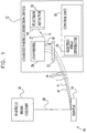
- System 10 comprises a charged particle detection device 12 configured according to the invention for detecting charged particle(s) 14 of different types emitted from a sample 16, and a particle beam column 18.
- Particle beam column 18 may comprise a focused ion beam (FIB) column, a dual beam column, an electron beam column, a helium beam column or any other suitable particle beam column.
- the charged particle detectable by detection device 12 is an electron, a positive ion or a negative ion.
- a particle beam 20, generated by column 18, irradiates the sample 16 causing charged particle (positive/negative ion and/or electron) emission from the sample 16. The emitted particle propagates towards detection device 12.
- the detection device 12 is operable in three modes for detecting positive and negative ions and electrons, respectively, depending on a generated electric field.
- the detection device 12 comprises a converter 26 for generating electrons 27 in response to interaction with incident charged particles 14, an electron detector 28, and a control unit 30.
- the detection system 10 comprises a grid electrode 32 accommodated in the path of charged particles emitted from the same, e.g. upstream of the converter 26 with respect to propagation of the charged particle trajectories. Grid 32 may or may not be a constructional part of the detection device 12.
- the control unit 30 comprises an electric field generator 38, which may be referred to as an electrical biasing assembly, configured and operable for creating an appropriate electric field within the detection device 12 to thereby define trajectories for charged particle (i.e. for positive and negative ion and for electron) propagation towards detector 28.
- Electric field generator 38 thus comprises a voltage supply unit (not shown) to supply/maintain appropriate voltages to converter 26 and detector 28 and also to grid 32 if such grid is used in the detection device 12.
- the converter 26 has a charged particle conversion surface 40 which has a continuous surface interaction region R oriented to intersect the trajectories of charged particles of different types. Conversion surface 40 (at least within the interaction region R ) is adapted for emitting electrons in response to interaction with incident charged particle(s). Electron detector 28 has a scintillator element surface 44 exposed to electron output from the converter 26. With such appropriately oriented continuous interaction region R, the electric field created within the detection device 12 defines an operational mode of the device to selectively allow detection of the charged particles of any type by the electron detector 28.
- electron detector 28 may be of any suitable configuration for receiving electrons and generating output data indicative thereof.
- MCP Multi-Channel-Plate
- SSD Solid State Diode
- CHANNELTRON® detector may be employed and may be commercially available at Burle Industries, Inc. of 1000 New Holland Avenue, Lancaster, PA 17601-5688 U.S.A.
- Detection device 12 thus operates as a triple mode particle detection device.
- converter 26 is electrically biasable for selectively attracting a charged particle and electron detector 28 is electrically biasable with respect to converter 26 so as to detect the electron emitted from the conversion surface 40.
- the scintillator element surface 44 of the electron detector 28 may be set to a positive high potential typically in the range of approximately 7kV-12kV.
- the converter 26 may be set to a positive or negative potential with a fixed proportion factor relative to the grid 32.
- the fixed proportion factor may be larger than 1, such as approximately 1.4, for example.
- the converter 26 and detector 28 may be each set at a different electrical potential to create an appropriate electric field defining the trajectories of the different-type charged particles so as to selectively facilitate detection of a positive ion in a positive ion detection mode, a negative ion in a negative ion detection mode, and an electron in an electron detection mode.
- grid 32 may be set to an electrical potential of approximately -2.7 kV
- converter 26 may be set to an electrical potential of approximately -3.8 kV
- the scintillator element surface 44 may be set to an electrical potential of approximately +10 kV.
- grid 32 may be set to an electrical potential of approximately +2.7 kV, converter 26 may be set to an electrical potential of approximately +3.8 kV and the scintillator element surface 44 may be set to an electrical potential of approximately +10 kV.
- grid 32 may be set to an electrical potential of approximately +1 kV, converter 26 may be set to an electrical potential of approximately +1.4 kV and the scintillator element surface 44 may be set to an electrical potential of approximately +10 kV.
- grid 32 may be located at any suitable location.
- the provision of the grid 32 is optional.
- the desired electric fields can be created by appropriate potentials on the converter 26 and detector 28 (to ensure that a particle 14 emitted from a sample 16 impinges upon the conversion surface 40 of the converter 26, and also to ensure that electrons 27 from the converter 26 are directed to the detector 28 ).
- the following description comprises some specific but non limiting examples of the configuration of the detection system according to the invention.
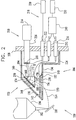
- FIG. 2 is a simplified sectional illustration of a particle detection system 100 constructed and operative in accordance with an embodiment of the present invention.
- Particle detection system 100 comprises a particle beam 102 generated by a beam column 104, and a charged particle detection device, also referred to as a triple mode particle detection device, which in the present example is located within a detection system chamber 106 having walls 108.
- the particle beam 102 generated by column 104 irradiates a sample 110 thus urging one or more charged particles 114 to be emitted therefrom.
- the emitted charged particles 114 may comprise an electron, positive ion and/or a negative ion.
- beam column 104 may comprise a focused ion beam (FIB) column, a dual beam column, an electron beam column, a helium beam column or any other suitable particle beam column.
- FIB focused ion beam
- a particle detection device 120 is enclosed in a housing 124 formed of any suitable conductive material.
- housing 124 is set to an electrical potential of the detection system chamber 106.
- a grid 130 is provided in the detection device, e.g. being mounted to walls 134 and 138 of the housing 124 in any suitable manner, e.g. using mounting elements 140 and 142.
- Mounting elements 140 and 142 may be formed of any suitable material, typically an insulating material, such as Ertalyte® which may be commercially available at Modem Plastics of 678 Howard Avenue, Bridgeport, Connecticut, USA.
- Housing 124 has an aperture 150 in its wall 134 for a charged particle 114 to pass therethrough.
- charged particle 114 is urged to pass the housing aperture 150 and reach grid 130 while the electric field in the detection device is such as to attract the particle towards the grid 130 (the grid 130 is electrically biased at a potential operative to attract the charged particle 114 thereto).
- Grid 130 may be formed of any suitable conductive material, such as stainless steal.
- the grid 130 may define a planar surface 152 or any other suitable geometry, such as a curved surface, a mash, an array of spaced apart elements or any configuration operative to allow a particle to pass therethrough.
- the charged particle 114 passes grid 130, via a grid space/aperture 156, preferably configured at a central location of planer surface 152, and propagates to a converter 160.
- Converter 160 may have any suitable configuration such that a conversion surface 164 thereof, or at least an interaction region R thereof, is located in the propagation path of the charged particles of different types. As seen in Fig. 2 , a cross section of converter 160 may have a right triangle geometry with conversion surface 164 defined by a hypotenuse surface between side supports 168. Converter 160 may include a bottom support 170, thus defining a converter vicinity 172 therein for charged particle passage therethrough away from the conversion surface 164. Bottom support 170 is formed with an aperture 180 for charged particle passage therethrough towards the conversion surface 164.
- Converter 160 may be mounted to housing 124 in any suitable manner, such as by a mounting element 174 affixing conversion surface 164 to housing wall 138.
- Mounting element 174 may be formed of any suitable material, typically an insulating material, such as Ertalyte® which may be commercially available at Modem Plastics of 678 Howard Avenue, Bridgeport, Connecticut, USA.
- Any suitable material for allowing high electron emission may be used for the conversion surface 164 of converter 160, such as aluminum covered by a thin layer of aluminum oxide, for example.
- a control unit ( Fig. 1 ), namely its electric field generator operates to create an appropriate electric field to direct charged particle 114 towards the converter 160, i.e. converter 160 is electrically biased at a potential operative to attract the charged particle 114 thereto such that the charged particle 114 passes aperture 180 and impinges upon conversion surface 164 within the interaction region R at its surface side 192. Consequentially, a plurality of electrons 194 are emitted from conversion surface 164 at the same surface side 192.
- converter 160 operates as an ion-to-electron converter whereupon the charged particle 114 is a positive ion or a negative ion.
- the same conversion surface operates as a particle 114 amplifier. For example, three electrons 194 may be emitted upon impingement of a single particle 114 on conversion surface 164.
- the so-emitted electrons 194 pass vicinity 172 and propagate towards a scintillator element surface 200 of an electron detector 210.
- the scintillator element surface 200 may be coupled to a light sensor, such as a photomultiplier tube (PMT) 214 via a light guide 216 thereby yielding an electrical signal from electron detector 210.
- PMT photomultiplier tube
- the grid 130, converter 160 and scintillator element surface 200 are electrically biased so as to create an electric field capable of urging charged particle 114 of a specific type emitted from sample 110 to pass grid 130 onto converter 160 and to attract resultant electrons emitted from converter 160 to scintillator element surface 200.
- grid 130, converter 160 and scintillator element surface 200 may be electrically biased in any suitable manner.
- provision of grid 130 is optional. In the case no grid is used the electric field is defined by voltage on the converter 160 and scintillator element surface 200.
- an electrical biasing assembly 218 of control unit comprises a switchable high voltage power supply 220 coupled to a first voltage feedthrough 222 in electrical communication with scintillator element surface 200 so as to electrically bias scintillator element surface 200, and a switchable high voltage bipolar power supply 230 coupled to a second and a third voltage feedthrough 232 and 234, respectively, via a voltage divider 240.
- Second voltage feedthrough 232 is in electrical communication with converter 160 so as to electrically bias converter 160
- third voltage feedthrough 234 is in electrical communication with grid 130 so as to electrically bias grid 130.
- electrical biasing assembly 218 may be configured in any suitable configuration, such as will be exemplified hereinbelow with reference to Fig. 3 .
- a plurality or single voltage power supply may be provided.
- the control unit may be located within particle detection system 100 or may be located externally to particle detection system 100 and is in electrical communication therewith.
- the voltage power supply and/or the voltage divider may be located within particle detection system 100 or may be located externally to particle detection system 100 and are in electrical communication therewith.
- the converter 160 (and also grid 130 if used) is positioned relative to sample 110 and is electrically biased so as to ensure that a charged particle 114 emitted from sample 110 is attracted to the interaction region R within the conversion surface of converter 160. Additionally, the converter 160 (and grid 130 if used) may be positioned relative to sample 110 and the converter 160 and scintillator element surface 200 are electrically biased so as to ensure that a charged particle 114 impinges upon the interaction region within the conversion surface 164 at a location where an attraction force generated by scintillator element surface 200 is greatest so as to ensure that a resultant electron emitted from conversion surface 164 is attracted to scintillator element surface 200. This location, designated by reference numeral 250 in Fig. 2 , is proximal to the scintillator element surface 200.
- grid 130 may be located at any suitable location inside or outside the housing 124. Additionally, grid 130 may be obviated and converter 160 may be thus electrically biased so as to ensure that a particle 114 emitted from sample 110 will impinge upon conversion surface 164.
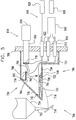
- Particle detection system 300 comprises a particle beam 302 generated by a particle beam column 304 which in the present example is located within a detection system chamber 306 defined by chamber walls 308, and a triple mode particle detection device.
- the particle beam 302 generated by column 304 irradiates a sample 310 thus causing a charged particle 314 to be emitted therefrom.
- the charged particle 314 may be an electron, positive ion or a negative ion.
- Beam column 304 may comprise an FIB column, a dual beam column, an electron beam column, a helium beam column or any other suitable particle beam column.
- Triple mode particle detection device 320 comprises a housing 324, and optionally comprises a grid 330 which may be located inside or outside the housing 324.
- the housing is formed of any suitable conductive material, and is preferably set to an electrical potential of the detection system chamber 306.
- grid 330 is located inside the housing 324 being appropriately mounted to housing walls 334 and 338, e.g. using mounting elements 340 and 342.
- Charged particle 314 is directed, by electric field in the detection device, to pass a housing aperture 350 in wall 334 and reach grid 330 which is electrically biased at a potential operative to attract the charged particle 314 thereto.
- grid 330 may be formed of any suitable conductive material, such as stainless steal, and may define any suitable configuration such as a planar surface or a curved surface 352 allowing a particle 314 to pass through grid aperture/space 356.
- the latter is preferably configured at a central location of planer surface 352.
- Converter 360 may have any suitable configuration. As exemplified in Fig. 3 , converter 360 has a geometry similar to that of Fig. 2 , namely having a right triangle cross section with a conversion surface 364, defined by a hypotenuse surface, between side supports 368. Converter 360 may include a bottom surface 370 thus defining a converter vicinity therein 372 for charged particle passage therethrough away from the conversion surface 364. Bottom support 370 is formed with an aperture 380 for charged particle passage therethrough towards the conversion surface 364. Converter 360 may be mounted to housing 324 by a mounting element 374 affixing conversion surface 364 to housing wall 338. Any suitable material for allowing high electron emission may be used for the conversion surface of converter 360, such as aluminum covered by a thin layer of aluminum oxide, for example.
- Converter 360 is electrically biased at a potential operative to attract the charged particle 314 thereto such that the charged particle 314 passes aperture 380 and impinges upon conversion surface 364. Consequentially, a plurality of electrons 390 are emitted from conversion surface 364 at the same surface side 392 onto which the charged particle 314 was incident. Thus, converter 360 operates as an ion-to-electron converter whereupon the charged particle 314 is a positive ion or a negative ion. Additionally, the same conversion surface operates as a particle 314 amplifier. For example, three electrons 390 may be emitted upon impingement of a single particle 314 on conversion surface 364.
- Electrons 390 pass vicinity 372 and impinge upon a scintillator element surface 400 of an electron detector 410.
- the scintillator element surface 400 may be coupled to a light sensor, such as a PMT 414 via a light guide 416 thereby yielding an electrical signal from electron detector 410.
- an electrical biasing assembly 418 comprises a switchable high voltage power supply 420 coupled to a first voltage feedthrough 422 in electrical communication with scintillator element surface 400 so as to electrically bias scintillator element surface 400, and a switchable high voltage power supply 430 coupled to a second voltage feedthrough 432 which is in electrical communication with converter 360.
- Resistors 440 and 442 may be provided so as to allow voltage fed via voltage feedthrough 432 to be divided between grid 330 and converter 360 in order to electrically bias them. As seen in Fig. 3 , resistors 440 are interconnected between housing 324 and second voltage feedthrough 432. Resistor 440 may be of approximately 2.5G ⁇ resistance and resistor 442 may be of approximately 1G ⁇ resistance. It is appreciated that a multiplicity of resistors may be utilized and may be located at various locations within detection device 320 at various degrees of resistance.
- the converter 360 is positioned relative to sample 310 and is electrically biased to ensure that a particle 314 emitted from sample 310 will be attracted to converter 360 (e.g. assisted by grid 330 ) and thereby impinge upon conversion surface 364. Additionally, the converter 360 (and grid 330 ) may be positioned relative to sample 310 and electrically biased to ensure that a particle 314 interacts with the conversion surface 364 at a location wherein an attraction force generated by scintillator element surface 400 is greatest so as to ensure that a resultant electron emitted from converter 360 is attracted to scintillator element surface 400. This location 450 is proximal to the scintillator element surface 400.
- grid 330 may be located at any suitable location inside or outside the housing 324. Additionally, grid 330 may not be used at all and converter 360 may be thus electrically biased so as to ensure that a particle 314 emitted from sample 310 interacts with conversion surface 364.
- FIG. 4 is a simplified sectional illustration of a particle detection system 500 constructed and operative in accordance with yet another embodiment of the present invention.
- Particle detection system 500 is configured generally similar to the above-described examples, namely comprising a particle beam 502 generated by a particle beam column 504 and a triple mode particle detection device 520.
- Column 504 may comprise an FIB column, a dual beam column, an electron beam column, a helium beam column or any other suitable particle beam column.
- Column 504 is located within a detection system chamber 506 defined by chamber walls 508, and operates to generate particle beam 502 to irradiate a sample 510 thus causing emission of a charged particle 514 (an electron, positive ion or a negative ion) from the sample 510.
- a charged particle 514 an electron, positive ion or a negative ion
- the detection device 520 has a housing 524 (formed of any suitable conductive material and is preferably set to an electrical potential of the detection system chamber 506 ) having an aperture 550 defined within a wall 534, optionally comprises a grid 530 (e.g. mounted to housing walls 534 and 538 by respective mounting elements 540 and 542 ), and comprises an electron detector 610.
- Charged particle 514 is urged to pass through aperture 550 towards grid 530, electrically biased at an appropriate potential operative to attract the charged particle 514 thereto, and to pass through a grid aperture/space 556 (e.g. at a central location of a planer surface 552 of the grid 530 ) to a converter 560.
- converter 560 has a curved conversion surface 564 between side supports 568.
- Converter 560 may include a bottom surface 570 defining a converter vicinity 572 for charged particle passage therethrough away from the conversion surface 564.
- Bottom support 570 is formed with an aperture 580 for charged particle passage therethrough towards the conversion surface 564.
- Converter 560 may be mounted to housing 524 by a mounting element 574 affixing conversion surface 564 to housing wall 538.
- Conversion surface 564 may be made of any suitable material allowing high electron emission therefrom, such as aluminum covered by a thin layer of aluminum oxide, for example.
- converter 560 is electrically biased at a potential operative to attract the charged particle 514 thereto such that the charged particle 514 passes aperture 580 and impinges upon conversion surface 564 at its surface side 592 resulting in emission of a plurality of electrons 590 from conversion surface 564 at the same surface side 592.
- converter 560 operates as an ion-to-electron converter whereupon the charged particle 514 is a positive ion or a negative ion.
- the same conversion surface operates as a particle 514 amplifier. For example, three electrons 590 may be emitted upon impingement of a single particle 514 on conversion surface 564.
- Electrons 590 pass vicinity 572 and impinge upon a scintillator element surface 600 of electron detector 610.
- the scintillator element surface 600 may be coupled to a light sensor, such as a PMT 614 via a light guide 616 thereby yielding an electrical signal from electron detector 610.
- converter 560 and scintillator element surface 600 are electrically biased so as to direct a charged particle 514 emitted from sample 510 towards an interaction region within the conversion surface of converter 560 (e.g. via grid 530 ) and to attract resultant electrons 590, emitted from converter 560, to scintillator element surface 600.
- Converter 560 and scintillator element surface 600 may be electrically biased using an electrical biasing assembly 618 comprising a switchable high voltage power supply 620 coupled to a first voltage feedthrough 622 in electrical communication with scintillator element surface 600 so as to electrically bias scintillator element surface 600, and a switchable high voltage bipolar power supply 630 coupled to a second and a third voltage feedthrough 632 and 634, respectively, via a voltage divider 640.
- Second voltage feedthrough 632 is in electrical communication with converter 560 so as to electrically bias it
- third voltage feedthrough 634 is in electrical communication with grid 530 so as to electrically bias grid 530.
- the conversion surface 564 may be shaped so as to minimize inhomogeneities in a detection efficiency of the charged particles 514 irrespective of their location along an interaction region R of the conversion surface 564.
- the detection efficiency is defined as the conversion factor of a charged particle 514 impinging on conversion surface 564, i.e. the number of electrons 590 emitted from conversion surface 564 per single impinging charged particle 514, multiplied by the extraction efficiency of the emitted electrons 590, i.e. the probability that an emitted electron 590 will impinge on the scintillator element surface 600.
- the attraction force of the scintillator element surface 600 defined by the electrical field generated by the scintillator element surface 600 in the detection device may decrease as the detection distance, i.e. the distance of a location on the conversion surface 564 from the scintillator element surface 600, increases.
- the extraction efficiency may decrease as the detection distance increases and in turn the detection efficiency may be inhomogenous along conversion surface 564.
- the conversion surface 564 is shaped so as to increase the conversion factor as the detection distance increases.
- the conversion factor may increase as a grazing angle of a particle 514 impinging on the conversion surface 564 decreases.
- the conversion factor will increase as the detection distance increases and thus the detection efficiency inhomogeneity along the conversion surface 564 is minimized.
- Fig. 4 it is seen that due to the curvature of the conversion surface 564, at a location 660 on conversion surface 564, which is in relative proximity to the scintillator element surface 600, the grazing angle 664 of a particle 666 impinging on conversion surface 564 is relatively large. Accordingly, at a location 670 on conversion surface 564, which is in relative distance to the scintillator element surface 600, the grazing angle 674 of a particle 676 impinging on conversion surface 564 is relatively small, thus the efficiency inhomogeneity along the conversion surface 564 is minimized.
- the conversion factor at a normal incidence angle is 5.27 and increases to 19.75 wherein the grazing angle is 10°.
- the curvature of the conversion surface 564 may be determined in accordance with the specific parameters, such as the detection distance, for example, of a given particle detection system. This can be achieved by simulating impingement of particles on a conversion surface within a given particle detection system so as to determine the optimal conversion surface curvature operative to provide a homogenous detection efficiency along the conversion surface.
- curvature of conversion surface 564 may be formed with a constant radius of curvature or, alternatively, with a variable radius of curvature.
- grid 530 may be located at any suitable location inside or outside the housing 524, and may not be used at all, in which case converter 560 is appropriately electrically biased to ensure that a charged particle 514 emitted from sample 510 will impinge upon conversion surface 564.
- Particle detection system 700 comprises a particle beam 702 generated by a particle beam column 704, which may comprise an FIB column, a dual beam column, an electron beam column, a helium beam column or any other suitable particle beam column.
- Column 704 is located within a detection system chamber 706 defined by chamber walls 708, and operates to generate particle beam 702 to irradiate a sample 710 thus causing emission of a charged particle 714 (an electron, positive ion or a negative ion) from the sample 710.
- a charged particle 714 an electron, positive ion or a negative ion
- a detection device 720 comprises a housing 724 (formed of any suitable conductive material and is preferably set to an electrical potential of the detection system chamber 706 ), a grid 730 (the provision of which is optional) mounted to housing walls 734 and 738 by respective mounting elements 740 and 742, a converter 760 and an electron detector 810.
- the charged particle 714 is directed to pass a housing aperture 750 defined within wall 734 towards grid 730 due to an appropriate electric field obtained by electrically biasing the grid 730 at a potential operative to attract the charged particle 714 thereto.
- the charged particle 714 passes grid 730 to converter 760, via a grid aperture 756, preferably configured at a central location of planer surface 752 defined by grid 730.
- Converter 760 may be formed with a conversion surface 764 defining a substantially planar continuous interaction region R.
- the planar conversion surface 764 is seen in Fig. 5 to be generally perpendicular to a scintillator element surface 770 described in further detail hereinbelow.
- Converter 760 may be mounted to housing 724 by a mounting element 774 affixing conversion surface 764 to housing wall 738 .
- Converter 760 is electrically biased at a potential operative to attract the charged particle 714 thereto such that the charged particle 714 impinges upon conversion surface 764 at its surface side 792, and a plurality of electrons 790 are emitted from said surface side 792.
- converter 760 operates as an ion-to-electron converter whereupon the charged particle 714 is a positive ion or a negative ion.
- the same conversion surface operates as a particle 714 amplifier. For example, three electrons 790 may be emitted upon impingement of a single particle 714 on conversion surface 764 .
- Electrons 790 impinge upon scintillator element surface 770 of electron detector 810 .
- the scintillator element surface 770 may be coupled to a light sensor, such as a photomultiplier tube 814 via a light guide 816 thereby yielding an electrical signal from electron detector 810 .
- Converter 760 and scintillator element surface 770 are electrically biased so as to force a charged particle 714 emitted from sample 710 to pass to the interaction region R within the conversion surface of converter 760 and to attract resultant electrons 790 emitted from converter 760 to scintillator element surface 770.
- Converter 760 and scintillator element surface 770 are appropriately electrically biased to create a desired electric field defining the trajectories of the emitted charged particle to interact with the converter. In the embodiment shown in Fig.
- an electrical biasing assembly 818 comprises a switchable high voltage power supply 820 coupled to a first voltage feedthrough 822 in electrical communication with scintillator element surface 770 so as to electrically bias scintillator element surface 770 , and a switchable high voltage bipolar power supply 830 coupled to a second and a third voltage feedthrough 832 and 834, respectively, via a voltage divider 840 .
- Second voltage feedthrough 832 is in electrical communication with converter 760 so as to electrically bias converter 760
- third voltage feedthrough 834 is in electrical communication with grid 730 so as to electrically bias grid 730.
- the converter 760 (and grid 730 ) may be positioned relative to sample 710 and may be electrically biased to ensure that a charged particle 714 emitted from sample 710 will be attracted to the interaction region R of converter 760. Additionally, the converter 760 (and grid 730 ) may be positioned relative to sample 710 and may be electrically biased to ensure that a charged particle 714 interacts with the conversion surface 764 at a location wherein an attraction force generated by scintillator element surface 770 is greatest so as to ensure that a resultant electron emitted from converter 760 is attracted to scintillator element surface 770. This location 850 is proximal to the scintillator element surface 770.
Landscapes
- Chemical & Material Sciences (AREA)
- Analytical Chemistry (AREA)
- Measurement Of Radiation (AREA)
- Analysing Materials By The Use Of Radiation (AREA)
- Electron Tubes For Measurement (AREA)
Description
- Applicant hereby claims priority of U. S. Patent Application Serial No. 12/155,233, filed on May 30, 2008, entitled "Three Modes Particle Detector".
- The present invention generally relates to a charged particle detection system and method, in particular to a particle detection system capable of detecting electrons, positive ions and negative ions.
- Electrons, positive ions and negative ions are charged particles that can be emitted from a sample upon irradiation thereof by a focused ion beam. Particle detectors, which can detect both positively charged particles and negatively charged particles, are well known. These detectors typically comprise a scintillator element, which is excited by electrons that are emitted from the sample and/or generated by conversion of ions to electrons by an ion-to-electron converter. The converters used in the devices of the kind specified are designed in such a way that positive ions are allowed to impinge upon surfaces of the ion-to-electron converter and cause emission of secondary electrons from the conversion surfaces of the converter, while negatively charged particles bypass the conversion surfaces without interacting with these surfaces.
- Publication
JP 63 07 1680 A -
US Patent No. 5 202 561 discloses a detector device for analyzing ions of high mass using a time-of-flight (TOF) analytical method, consisting of a mass spectrometer, accelerating electrodes and a magnetic field and/or electric field, all of which serves to deflect secondary ions emerging from a first conversion dynode, so that the secondary ions impinge according to polarity on a second and third conversion dynode. -
US Patent No. 3 898 456 relates to an improved ion detector for use in mass spectrometers for pulse counting single ions which may have a positive or a negative charge. The invention combines a novel electron multiplier with a scintillator type of ion detector. It is a high vacuum, high voltage device intended for use in ion microprobe mass spectrometers. - Publication
EP 0 278 034 A1 discloses a detector for detecting charged particles, the detector comprises a secondara electron multiplier for converting the charged particles into secondary electrons and amplifying the secondary electrons, a scintillator for converting the secondary electrons generated from the secondary electron multipler into light, and a photomultiplier for receiving the light. - The present invention provides a novel particle detection system capable of detecting electrons, positive ions and negative ions.
- The conventional particle detectors utilize ion-to-electron converters and are configured to allow positive ion interaction with the conversion surfaces of the converter while preventing negative ion and electron interaction with such surfaces. However, with the conventional approach, negative ions pass through a detector and impinge directly upon the surface of a scintillator element thus shortening the scintillator element surface life.
- The invented approach provides for solving the above problem. Also, the invention provides for utilizing the ion-to-electron converter for converting electrons originating from a sample to secondary electrons, in addition to converting the positive and negative ions to electrons, thereby amplifying the number of electrons to be detected by the detector.
- There is thus provided a charged particle detection device and system according to claims 1 and 7, respectively, and a method for use in detecting charged particles according to
claim 10. Advantageous embodiments of the invention are set out in the dependent claims. - The present invention will be understood and appreciated more folly from the following detailed description, taken in conjunction with the drawings in which
-
Fig. 1 is a schematic illustration of an example of a charged particle detection system according to the invention; -
Fig. 2 is a simplified sectional illustration of a particle detection system constructed and operative in accordance with an embodiment of the present invention; -
Fig. 3 is a simplified sectional illustration of a particle detection system constructed and operative in accordance with another embodiment of the present invention; -
Fig. 4 is a simplified sectional illustration of a particle detection system constructed and operative in accordance with yet another embodiment of the present invention; and -
Fig. 5 is a simplified sectional illustration of a particle detection system constructed and operative in accordance with still another embodiment of the present invention. - Referring to
Fig. 1 , there is illustrated, by way of a block diagram, an example of a chargedparticle detection system 10 configured and operable according to the invention.System 10 comprises a chargedparticle detection device 12 configured according to the invention for detecting charged particle(s) 14 of different types emitted from asample 16, and aparticle beam column 18.Particle beam column 18 may comprise a focused ion beam (FIB) column, a dual beam column, an electron beam column, a helium beam column or any other suitable particle beam column. The charged particle detectable bydetection device 12 is an electron, a positive ion or a negative ion. Aparticle beam 20, generated bycolumn 18, irradiates thesample 16 causing charged particle (positive/negative ion and/or electron) emission from thesample 16. The emitted particle propagates towardsdetection device 12. - As will be described further below, the
detection device 12 is operable in three modes for detecting positive and negative ions and electrons, respectively, depending on a generated electric field. Thedetection device 12 comprises aconverter 26 for generatingelectrons 27 in response to interaction with incidentcharged particles 14, anelectron detector 28, and acontrol unit 30. Optionally, thedetection system 10 comprises agrid electrode 32 accommodated in the path of charged particles emitted from the same, e.g. upstream of theconverter 26 with respect to propagation of the charged particle trajectories.Grid 32 may or may not be a constructional part of thedetection device 12. - The
control unit 30 comprises anelectric field generator 38, which may be referred to as an electrical biasing assembly, configured and operable for creating an appropriate electric field within thedetection device 12 to thereby define trajectories for charged particle (i.e. for positive and negative ion and for electron) propagation towardsdetector 28.Electric field generator 38 thus comprises a voltage supply unit (not shown) to supply/maintain appropriate voltages to converter 26 anddetector 28 and also togrid 32 if such grid is used in thedetection device 12. - The
converter 26 has a chargedparticle conversion surface 40 which has a continuous surface interaction region R oriented to intersect the trajectories of charged particles of different types. Conversion surface 40 (at least within the interaction region R) is adapted for emitting electrons in response to interaction with incident charged particle(s).Electron detector 28 has ascintillator element surface 44 exposed to electron output from theconverter 26. With such appropriately oriented continuous interaction region R, the electric field created within thedetection device 12 defines an operational mode of the device to selectively allow detection of the charged particles of any type by theelectron detector 28. - It is appreciated that
electron detector 28 may be of any suitable configuration for receiving electrons and generating output data indicative thereof. For example, a Multi-Channel-Plate (MCP) or a Solid State Diode (SSD) may be employed. Alternatively, a CHANNELTRON® detector may be employed and may be commercially available at Burle Industries, Inc. of 1000 New Holland Avenue, Lancaster, PA 17601-5688 U.S.A. -
Detection device 12 thus operates as a triple mode particle detection device. As will be described more specifically further below,converter 26 is electrically biasable for selectively attracting a charged particle andelectron detector 28 is electrically biasable with respect to converter 26 so as to detect the electron emitted from theconversion surface 40. - In a non-limiting example, the
scintillator element surface 44 of theelectron detector 28 may be set to a positive high potential typically in the range of approximately 7kV-12kV. Theconverter 26 may be set to a positive or negative potential with a fixed proportion factor relative to thegrid 32. The fixed proportion factor may be larger than 1, such as approximately 1.4, for example. - The
converter 26 and detector 28 (its scintillator element surface 44), as well asgrid 32 if used, may be each set at a different electrical potential to create an appropriate electric field defining the trajectories of the different-type charged particles so as to selectively facilitate detection of a positive ion in a positive ion detection mode, a negative ion in a negative ion detection mode, and an electron in an electron detection mode. For example, to facilitate the positive ion detection mode,grid 32 may be set to an electrical potential of approximately -2.7 kV,converter 26 may be set to an electrical potential of approximately -3.8 kV and thescintillator element surface 44 may be set to an electrical potential of approximately +10 kV. To implement the negative ion detection mode,grid 32 may be set to an electrical potential of approximately +2.7 kV,converter 26 may be set to an electrical potential of approximately +3.8 kV and thescintillator element surface 44 may be set to an electrical potential of approximately +10 kV. In the electron detection mode,grid 32 may be set to an electrical potential of approximately +1 kV,converter 26 may be set to an electrical potential of approximately +1.4 kV and thescintillator element surface 44 may be set to an electrical potential of approximately +10 kV. - It is appreciated that
grid 32, if used, may be located at any suitable location. The provision of thegrid 32 is optional. The desired electric fields can be created by appropriate potentials on theconverter 26 and detector 28 (to ensure that aparticle 14 emitted from asample 16 impinges upon theconversion surface 40 of theconverter 26, and also to ensure thatelectrons 27 from theconverter 26 are directed to the detector 28). The following description comprises some specific but non limiting examples of the configuration of the detection system according to the invention. - Reference is made to
Fig. 2 , which is a simplified sectional illustration of aparticle detection system 100 constructed and operative in accordance with an embodiment of the present invention.Particle detection system 100 comprises aparticle beam 102 generated by abeam column 104, and a charged particle detection device, also referred to as a triple mode particle detection device, which in the present example is located within adetection system chamber 106 havingwalls 108. Theparticle beam 102 generated bycolumn 104 irradiates asample 110 thus urging one or more chargedparticles 114 to be emitted therefrom. The emitted chargedparticles 114 may comprise an electron, positive ion and/or a negative ion. As indicated above,beam column 104 may comprise a focused ion beam (FIB) column, a dual beam column, an electron beam column, a helium beam column or any other suitable particle beam column. - A
particle detection device 120 is enclosed in ahousing 124 formed of any suitable conductive material. Preferably,housing 124 is set to an electrical potential of thedetection system chamber 106. Optionally, agrid 130 is provided in the detection device, e.g. being mounted towalls housing 124 in any suitable manner, e.g. using mountingelements elements -
Housing 124 has anaperture 150 in itswall 134 for a chargedparticle 114 to pass therethrough. Thus, chargedparticle 114 is urged to pass thehousing aperture 150 and reachgrid 130 while the electric field in the detection device is such as to attract the particle towards the grid 130 (thegrid 130 is electrically biased at a potential operative to attract the chargedparticle 114 thereto).Grid 130 may be formed of any suitable conductive material, such as stainless steal. Thegrid 130 may define aplanar surface 152 or any other suitable geometry, such as a curved surface, a mash, an array of spaced apart elements or any configuration operative to allow a particle to pass therethrough. - The charged
particle 114passes grid 130, via a grid space/aperture 156, preferably configured at a central location ofplaner surface 152, and propagates to aconverter 160.Converter 160 may have any suitable configuration such that aconversion surface 164 thereof, or at least an interaction region R thereof, is located in the propagation path of the charged particles of different types. As seen inFig. 2 , a cross section ofconverter 160 may have a right triangle geometry withconversion surface 164 defined by a hypotenuse surface between side supports 168.Converter 160 may include abottom support 170, thus defining aconverter vicinity 172 therein for charged particle passage therethrough away from theconversion surface 164.Bottom support 170 is formed with an aperture 180 for charged particle passage therethrough towards theconversion surface 164.Converter 160 may be mounted tohousing 124 in any suitable manner, such as by a mountingelement 174 affixingconversion surface 164 tohousing wall 138. Mountingelement 174 may be formed of any suitable material, typically an insulating material, such as Ertalyte® which may be commercially available at Modem Plastics of 678 Howard Avenue, Bridgeport, Connecticut, USA. - Any suitable material for allowing high electron emission may be used for the
conversion surface 164 ofconverter 160, such as aluminum covered by a thin layer of aluminum oxide, for example. - A control unit (
Fig. 1 ), namely its electric field generator operates to create an appropriate electric field to direct chargedparticle 114 towards theconverter 160, i.e.converter 160 is electrically biased at a potential operative to attract the chargedparticle 114 thereto such that the chargedparticle 114 passes aperture 180 and impinges uponconversion surface 164 within the interaction region R at its surface side 192. Consequentially, a plurality ofelectrons 194 are emitted fromconversion surface 164 at the same surface side 192. Thus,converter 160 operates as an ion-to-electron converter whereupon the chargedparticle 114 is a positive ion or a negative ion. Additionally, the same conversion surface operates as aparticle 114 amplifier. For example, threeelectrons 194 may be emitted upon impingement of asingle particle 114 onconversion surface 164. - The so-emitted
electrons 194pass vicinity 172 and propagate towards ascintillator element surface 200 of anelectron detector 210. Thescintillator element surface 200 may be coupled to a light sensor, such as a photomultiplier tube (PMT) 214 via alight guide 216 thereby yielding an electrical signal fromelectron detector 210. - As described hereinabove, the
grid 130,converter 160 andscintillator element surface 200 are electrically biased so as to create an electric field capable of urging chargedparticle 114 of a specific type emitted fromsample 110 to passgrid 130 ontoconverter 160 and to attract resultant electrons emitted fromconverter 160 toscintillator element surface 200. It should be understood thatgrid 130,converter 160 andscintillator element surface 200 may be electrically biased in any suitable manner. Also, provision ofgrid 130 is optional. In the case no grid is used the electric field is defined by voltage on theconverter 160 andscintillator element surface 200. - In the embodiment shown in
Fig. 2 , anelectrical biasing assembly 218 of control unit comprises a switchable highvoltage power supply 220 coupled to afirst voltage feedthrough 222 in electrical communication withscintillator element surface 200 so as to electrically biasscintillator element surface 200, and a switchable high voltagebipolar power supply 230 coupled to a second and athird voltage feedthrough voltage divider 240.Second voltage feedthrough 232 is in electrical communication withconverter 160 so as to electricallybias converter 160, andthird voltage feedthrough 234 is in electrical communication withgrid 130 so as to electricallybias grid 130. - It is appreciated that
electrical biasing assembly 218 may be configured in any suitable configuration, such as will be exemplified hereinbelow with reference toFig. 3 . Alternatively, a plurality or single voltage power supply may be provided. The control unit may be located withinparticle detection system 100 or may be located externally toparticle detection system 100 and is in electrical communication therewith. Additionally, the voltage power supply and/or the voltage divider may be located withinparticle detection system 100 or may be located externally toparticle detection system 100 and are in electrical communication therewith. - The converter 160 (and also
grid 130 if used) is positioned relative to sample 110 and is electrically biased so as to ensure that a chargedparticle 114 emitted fromsample 110 is attracted to the interaction region R within the conversion surface ofconverter 160. Additionally, the converter 160 (andgrid 130 if used) may be positioned relative to sample 110 and theconverter 160 andscintillator element surface 200 are electrically biased so as to ensure that a chargedparticle 114 impinges upon the interaction region within theconversion surface 164 at a location where an attraction force generated byscintillator element surface 200 is greatest so as to ensure that a resultant electron emitted fromconversion surface 164 is attracted toscintillator element surface 200. This location, designated byreference numeral 250 inFig. 2 , is proximal to thescintillator element surface 200. - It is appreciated that
grid 130 may be located at any suitable location inside or outside thehousing 124. Additionally,grid 130 may be obviated andconverter 160 may be thus electrically biased so as to ensure that aparticle 114 emitted fromsample 110 will impinge uponconversion surface 164. - It is noted that features described in reference to
Fig. 1 may be identical to features described in reference toFig. 2 . - Reference is now made to
Fig. 3 , which is a simplified sectional illustration of aparticle detection system 300 constructed and operative in accordance with another embodiment of the present invention.Particle detection system 300 comprises aparticle beam 302 generated by aparticle beam column 304 which in the present example is located within adetection system chamber 306 defined bychamber walls 308, and a triple mode particle detection device. Theparticle beam 302 generated bycolumn 304 irradiates asample 310 thus causing a chargedparticle 314 to be emitted therefrom. The chargedparticle 314 may be an electron, positive ion or a negative ion.Beam column 304 may comprise an FIB column, a dual beam column, an electron beam column, a helium beam column or any other suitable particle beam column. - Triple mode
particle detection device 320 comprises ahousing 324, and optionally comprises agrid 330 which may be located inside or outside thehousing 324. The housing is formed of any suitable conductive material, and is preferably set to an electrical potential of thedetection system chamber 306. In the present example,grid 330 is located inside thehousing 324 being appropriately mounted tohousing walls elements Charged particle 314 is directed, by electric field in the detection device, to pass ahousing aperture 350 inwall 334 and reachgrid 330 which is electrically biased at a potential operative to attract the chargedparticle 314 thereto. As indicated above,grid 330 may be formed of any suitable conductive material, such as stainless steal, and may define any suitable configuration such as a planar surface or acurved surface 352 allowing aparticle 314 to pass through grid aperture/space 356. The latter is preferably configured at a central location ofplaner surface 352. -
Charged particle 314 passes throughgrid 330 toward aconverter 360.Converter 360 may have any suitable configuration. As exemplified inFig. 3 ,converter 360 has a geometry similar to that ofFig. 2 , namely having a right triangle cross section with aconversion surface 364, defined by a hypotenuse surface, between side supports 368.Converter 360 may include abottom surface 370 thus defining a converter vicinity therein 372 for charged particle passage therethrough away from theconversion surface 364.Bottom support 370 is formed with anaperture 380 for charged particle passage therethrough towards theconversion surface 364.Converter 360 may be mounted tohousing 324 by a mountingelement 374 affixingconversion surface 364 tohousing wall 338. Any suitable material for allowing high electron emission may be used for the conversion surface ofconverter 360, such as aluminum covered by a thin layer of aluminum oxide, for example. -
Converter 360 is electrically biased at a potential operative to attract the chargedparticle 314 thereto such that the chargedparticle 314passes aperture 380 and impinges uponconversion surface 364. Consequentially, a plurality ofelectrons 390 are emitted fromconversion surface 364 at thesame surface side 392 onto which the chargedparticle 314 was incident. Thus,converter 360 operates as an ion-to-electron converter whereupon the chargedparticle 314 is a positive ion or a negative ion. Additionally, the same conversion surface operates as aparticle 314 amplifier. For example, threeelectrons 390 may be emitted upon impingement of asingle particle 314 onconversion surface 364. -
Electrons 390pass vicinity 372 and impinge upon ascintillator element surface 400 of anelectron detector 410. Thescintillator element surface 400 may be coupled to a light sensor, such as aPMT 414 via alight guide 416 thereby yielding an electrical signal fromelectron detector 410. - As described hereinabove,
converter 360 and scintillator element surface 400 (and alsogrid 330 if used) are electrically biased so as to cause a chargedparticle 314 emitted fromsample 310 to pass to converter 360 (e.g. through grid 330) and to attract resultant electrons emitted fromconverter 360 toscintillator element surface 400. In the embodiment shown inFig. 3 , anelectrical biasing assembly 418 comprises a switchable highvoltage power supply 420 coupled to afirst voltage feedthrough 422 in electrical communication withscintillator element surface 400 so as to electrically biasscintillator element surface 400, and a switchable highvoltage power supply 430 coupled to asecond voltage feedthrough 432 which is in electrical communication withconverter 360.Resistors voltage feedthrough 432 to be divided betweengrid 330 andconverter 360 in order to electrically bias them. As seen inFig. 3 ,resistors 440 are interconnected betweenhousing 324 andsecond voltage feedthrough 432.Resistor 440 may be of approximately 2.5GΩ resistance andresistor 442 may be of approximately 1GΩ resistance. It is appreciated that a multiplicity of resistors may be utilized and may be located at various locations withindetection device 320 at various degrees of resistance. - Thus, the
converter 360 is positioned relative to sample 310 and is electrically biased to ensure that aparticle 314 emitted fromsample 310 will be attracted to converter 360 (e.g. assisted by grid 330) and thereby impinge uponconversion surface 364. Additionally, the converter 360 (and grid 330) may be positioned relative to sample 310 and electrically biased to ensure that aparticle 314 interacts with theconversion surface 364 at a location wherein an attraction force generated byscintillator element surface 400 is greatest so as to ensure that a resultant electron emitted fromconverter 360 is attracted toscintillator element surface 400. Thislocation 450 is proximal to thescintillator element surface 400. - As indicated above,
grid 330 may be located at any suitable location inside or outside thehousing 324. Additionally,grid 330 may not be used at all andconverter 360 may be thus electrically biased so as to ensure that aparticle 314 emitted fromsample 310 interacts withconversion surface 364. - Reference is now made to
Fig. 4 , which is a simplified sectional illustration of aparticle detection system 500 constructed and operative in accordance with yet another embodiment of the present invention.Particle detection system 500 is configured generally similar to the above-described examples, namely comprising aparticle beam 502 generated by aparticle beam column 504 and a triple modeparticle detection device 520.Column 504 may comprise an FIB column, a dual beam column, an electron beam column, a helium beam column or any other suitable particle beam column.Column 504 is located within adetection system chamber 506 defined bychamber walls 508, and operates to generateparticle beam 502 to irradiate asample 510 thus causing emission of a charged particle 514 (an electron, positive ion or a negative ion) from thesample 510. - Similar to the above examples, the
detection device 520 has a housing 524 (formed of any suitable conductive material and is preferably set to an electrical potential of the detection system chamber 506) having anaperture 550 defined within awall 534, optionally comprises a grid 530 (e.g. mounted tohousing walls elements 540 and 542), and comprises anelectron detector 610.Charged particle 514 is urged to pass throughaperture 550 towardsgrid 530, electrically biased at an appropriate potential operative to attract the chargedparticle 514 thereto, and to pass through a grid aperture/space 556 (e.g. at a central location of aplaner surface 552 of the grid 530) to aconverter 560. In the present non-limiting example,converter 560 has acurved conversion surface 564 between side supports 568.Converter 560 may include abottom surface 570 defining aconverter vicinity 572 for charged particle passage therethrough away from theconversion surface 564.Bottom support 570 is formed with anaperture 580 for charged particle passage therethrough towards theconversion surface 564.Converter 560 may be mounted tohousing 524 by a mountingelement 574 affixingconversion surface 564 tohousing wall 538.Conversion surface 564 may be made of any suitable material allowing high electron emission therefrom, such as aluminum covered by a thin layer of aluminum oxide, for example. - In order to create an appropriate electrical field within the detection device,
converter 560 is electrically biased at a potential operative to attract the chargedparticle 514 thereto such that the chargedparticle 514passes aperture 580 and impinges uponconversion surface 564 at itssurface side 592 resulting in emission of a plurality ofelectrons 590 fromconversion surface 564 at thesame surface side 592. Thus,converter 560 operates as an ion-to-electron converter whereupon the chargedparticle 514 is a positive ion or a negative ion. Additionally, the same conversion surface operates as aparticle 514 amplifier. For example, threeelectrons 590 may be emitted upon impingement of asingle particle 514 onconversion surface 564. -
Electrons 590pass vicinity 572 and impinge upon ascintillator element surface 600 ofelectron detector 610. As indicated above, thescintillator element surface 600 may be coupled to a light sensor, such as aPMT 614 via alight guide 616 thereby yielding an electrical signal fromelectron detector 610. - As described hereinabove,
converter 560 and scintillator element surface 600 (andgrid 530 if used) are electrically biased so as to direct a chargedparticle 514 emitted fromsample 510 towards an interaction region within the conversion surface of converter 560 (e.g. via grid 530) and to attractresultant electrons 590, emitted fromconverter 560, toscintillator element surface 600.Converter 560 and scintillator element surface 600 (andgrid 530 if used) may be electrically biased using anelectrical biasing assembly 618 comprising a switchable highvoltage power supply 620 coupled to afirst voltage feedthrough 622 in electrical communication withscintillator element surface 600 so as to electrically biasscintillator element surface 600, and a switchable high voltagebipolar power supply 630 coupled to a second and athird voltage feedthrough voltage divider 640.Second voltage feedthrough 632 is in electrical communication withconverter 560 so as to electrically bias it, andthird voltage feedthrough 634 is in electrical communication withgrid 530 so as to electricallybias grid 530. - In accordance with an embodiment of the present invention, the
conversion surface 564 may be shaped so as to minimize inhomogeneities in a detection efficiency of the chargedparticles 514 irrespective of their location along an interaction region R of theconversion surface 564. The detection efficiency is defined as the conversion factor of a chargedparticle 514 impinging onconversion surface 564, i.e. the number ofelectrons 590 emitted fromconversion surface 564 per single impinging chargedparticle 514, multiplied by the extraction efficiency of the emittedelectrons 590, i.e. the probability that an emittedelectron 590 will impinge on thescintillator element surface 600. It should be understood that the attraction force of thescintillator element surface 600 defined by the electrical field generated by thescintillator element surface 600 in the detection device may decrease as the detection distance, i.e. the distance of a location on theconversion surface 564 from thescintillator element surface 600, increases. Thus, the extraction efficiency may decrease as the detection distance increases and in turn the detection efficiency may be inhomogenous alongconversion surface 564. - In order to compensate for the decreasing extraction efficiency, the
conversion surface 564 is shaped so as to increase the conversion factor as the detection distance increases. Generally, the conversion factor may increase as a grazing angle of aparticle 514 impinging on theconversion surface 564 decreases. Thus by forming theconversion surface 564 as a concave surface, wherein the grazing angle decreases as the detection distance increases, the conversion factor will increase as the detection distance increases and thus the detection efficiency inhomogeneity along theconversion surface 564 is minimized. - Turning to
Fig. 4 , it is seen that due to the curvature of theconversion surface 564, at alocation 660 onconversion surface 564, which is in relative proximity to thescintillator element surface 600, thegrazing angle 664 of aparticle 666 impinging onconversion surface 564 is relatively large. Accordingly, at alocation 670 onconversion surface 564, which is in relative distance to thescintillator element surface 600, thegrazing angle 674 of aparticle 676 impinging onconversion surface 564 is relatively small, thus the efficiency inhomogeneity along theconversion surface 564 is minimized. In a non-limiting example, upon impingement of potassium particles on a conversion surface formed of aluminum oxide, the conversion factor at a normal incidence angle is 5.27 and increases to 19.75 wherein the grazing angle is 10°. - It is appreciated that the curvature of the
conversion surface 564 may be determined in accordance with the specific parameters, such as the detection distance, for example, of a given particle detection system. This can be achieved by simulating impingement of particles on a conversion surface within a given particle detection system so as to determine the optimal conversion surface curvature operative to provide a homogenous detection efficiency along the conversion surface. - It is further noted that the curvature of
conversion surface 564 may be formed with a constant radius of curvature or, alternatively, with a variable radius of curvature. - As indicated above,
grid 530 may be located at any suitable location inside or outside thehousing 524, and may not be used at all, in whichcase converter 560 is appropriately electrically biased to ensure that a chargedparticle 514 emitted fromsample 510 will impinge uponconversion surface 564. - Reference is now made to
Fig. 5 , which is a simplified sectional illustration of aparticle detection system 700 constructed and operative in accordance with still another embodiment of the present invention.Particle detection system 700 comprises aparticle beam 702 generated by aparticle beam column 704, which may comprise an FIB column, a dual beam column, an electron beam column, a helium beam column or any other suitable particle beam column.Column 704 is located within adetection system chamber 706 defined bychamber walls 708, and operates to generateparticle beam 702 to irradiate asample 710 thus causing emission of a charged particle 714 (an electron, positive ion or a negative ion) from thesample 710. - A
detection device 720 comprises a housing 724 (formed of any suitable conductive material and is preferably set to an electrical potential of the detection system chamber 706), a grid 730 (the provision of which is optional) mounted tohousing walls elements converter 760 and anelectron detector 810. The chargedparticle 714 is directed to pass ahousing aperture 750 defined withinwall 734 towardsgrid 730 due to an appropriate electric field obtained by electrically biasing thegrid 730 at a potential operative to attract the chargedparticle 714 thereto. - The charged
particle 714passes grid 730 toconverter 760, via agrid aperture 756, preferably configured at a central location ofplaner surface 752 defined bygrid 730.Converter 760 may be formed with aconversion surface 764 defining a substantially planar continuous interaction region R. Theplanar conversion surface 764 is seen inFig. 5 to be generally perpendicular to ascintillator element surface 770 described in further detail hereinbelow.Converter 760 may be mounted tohousing 724 by a mountingelement 774 affixingconversion surface 764 tohousing wall 738. -
Converter 760 is electrically biased at a potential operative to attract the chargedparticle 714 thereto such that the chargedparticle 714 impinges uponconversion surface 764 at itssurface side 792, and a plurality ofelectrons 790 are emitted from saidsurface side 792. Thus,converter 760 operates as an ion-to-electron converter whereupon the chargedparticle 714 is a positive ion or a negative ion. Additionally, the same conversion surface operates as aparticle 714 amplifier. For example, threeelectrons 790 may be emitted upon impingement of asingle particle 714 onconversion surface 764. -
Electrons 790 impinge uponscintillator element surface 770 ofelectron detector 810. Thescintillator element surface 770 may be coupled to a light sensor, such as aphotomultiplier tube 814 via alight guide 816 thereby yielding an electrical signal fromelectron detector 810. -
Converter 760 and scintillator element surface 770 (andgrid 730 if used) are electrically biased so as to force a chargedparticle 714 emitted fromsample 710 to pass to the interaction region R within the conversion surface ofconverter 760 and to attractresultant electrons 790 emitted fromconverter 760 toscintillator element surface 770.Converter 760 and scintillator element surface 770 (andgrid 730 if used) are appropriately electrically biased to create a desired electric field defining the trajectories of the emitted charged particle to interact with the converter. In the embodiment shown inFig. 5 anelectrical biasing assembly 818 comprises a switchable highvoltage power supply 820 coupled to afirst voltage feedthrough 822 in electrical communication withscintillator element surface 770 so as to electrically biasscintillator element surface 770, and a switchable high voltagebipolar power supply 830 coupled to a second and athird voltage feedthrough voltage divider 840.Second voltage feedthrough 832 is in electrical communication withconverter 760 so as to electricallybias converter 760 andthird voltage feedthrough 834 is in electrical communication withgrid 730 so as to electricallybias grid 730. - The converter 760 (and grid 730) may be positioned relative to sample 710 and may be electrically biased to ensure that a charged
particle 714 emitted fromsample 710 will be attracted to the interaction region R ofconverter 760. Additionally, the converter 760 (and grid 730) may be positioned relative to sample 710 and may be electrically biased to ensure that a chargedparticle 714 interacts with theconversion surface 764 at a location wherein an attraction force generated byscintillator element surface 770 is greatest so as to ensure that a resultant electron emitted fromconverter 760 is attracted toscintillator element surface 770. Thislocation 850 is proximal to thescintillator element surface 770. - It will be appreciated by persons skilled in the art that the present invention is not limited by what has been particularly shown and described herein above.
- The invention is limited only by the scope of the appended claims.
Claims (10)
- A charged particle detector device (12, 120) for detecting a charged particle emitted from a sample (16, 110), the detector device comprising:a converter (26,160) defining a conversion surface (40,164) with a continuous region (R) of interaction of incident charged particles of different types (14,114) comprising positive and negative ions and electrons, said conversion surface being adapted for emitting electrons (27,194) in response to interaction with the charged particles of different types;an electron detector (28, 210) for receiving electrons from the converter and generating output data indicative thereof, andan electric field generator (38) configured and operable to create an electric field defining trajectories for charged particles of different types (14,114) emitted from the sample (16, 110) as a result of the sample interaction with a particle beam (20,102), the emitted charged particles of different types being one of the following: electrons, positive ions and negative ions,said converter (26,160) having a conversion surface (40,164) comprising the continuous interaction region (R) oriented so as to intersect the trajectories of the charged particles of different types propagating from the sample, said conversion surface operative to emit electrons (27,194) in response to the surface interaction with the charged particles of different types,characterized in thatthe electric field created within the detection device defines an operational mode of the device to selectively allow detection of electrons, positive ions and negative ions.
- A device according to claim 1, wherein said conversion surface (40,164) is curved or planar.
- A device according to claim 1, wherein the converter (26,160) has a cross section of a right triangle geometry with a hypotenuse comprising said conversion surface (40,164) with the continuous interaction region (R).
- A device according to any one of claims 1-3, comprising a grid-like electrode (32, 130) accommodated upstream of the converter (26,160) for directing the charged particles (14,114) towards said interaction region (R).
- A device according to any one of claims 1-4, wherein said electron detector (28, 210) comprises a scintillator element surface (44, 200).
- A device according any one of claims 1-5, wherein the conversion surface (40,164) has a non-planar shape selected to minimize detection efficiency inhomogeneity within said device (12, 120).
- A charged particle detection system (10, 100) comprising:a particle beam column (18, 104) for generating a particle beam (20,102) for exciting the sample (16, 110) to thereby cause emission of charged particles of different types (14,114) therefrom, the emitted charged particles comprising at least one positive ion, negative ion and electron; anda charged particle detection device (12, 120) according to any one of one of claims 1-6.
- A system according to claim 7 and claim 4,
wherein the grid-like electrode (32, 130) is provided to direct the charged particles (14,114) emitted from the sample (16, 110) to said region (R) of interaction. - A system according to claim 7 or 8, wherein the particle beam column (18, 104) comprises a focused ion beam (FIB) column, a dual beam column, an electron beam column or a helium beam column.
- A method for use in detecting charged particles of different types (14,114) emitted from a sample (16, 110), the method comprising:creating an electric field in a path of charged particles of different types emitted from the sample so as to direct the charged particles of different types along a trajectory towards a charged particle converter (26,160), said charged particles of different types being one of the following: a positive ion, a negative ion and an electron;providing a continuous interaction region (R) of the converter oriented to intersect trajectories of the charged particles of different types propagating towards the converter, said interaction region being responsive to the charged particle incidence thereon to emit electrons (27,194); anddetecting the emitted electrons and generating output data indicative thereof,characterized in thatthe electric field created within the detection device defines an operational mode of the device to selectively allow detection of electrons, positive ions and negative ions.
Applications Claiming Priority (2)
| Application Number | Priority Date | Filing Date | Title |
|---|---|---|---|
| US12/155,233 US7847268B2 (en) | 2008-05-30 | 2008-05-30 | Three modes particle detector |
| PCT/IL2009/000534 WO2009144727A2 (en) | 2008-05-30 | 2009-05-31 | Charged particle detection system and method |
Publications (3)
| Publication Number | Publication Date |
|---|---|
| EP2297763A2 EP2297763A2 (en) | 2011-03-23 |
| EP2297763A4 EP2297763A4 (en) | 2012-05-30 |
| EP2297763B1 true EP2297763B1 (en) | 2016-07-06 |
Family
ID=41377680
Family Applications (1)
| Application Number | Title | Priority Date | Filing Date |
|---|---|---|---|
| EP09754346.6A Active EP2297763B1 (en) | 2008-05-30 | 2009-05-31 | Charged particle detection system and method |
Country Status (3)
| Country | Link |
|---|---|
| US (1) | US7847268B2 (en) |
| EP (1) | EP2297763B1 (en) |
| WO (1) | WO2009144727A2 (en) |
Cited By (1)
| Publication number | Priority date | Publication date | Assignee | Title |
|---|---|---|---|---|
| EP3622553B1 (en) * | 2017-05-12 | 2025-11-26 | Nova Measuring Instruments, Inc. | Mass spectrometer detector and system using the same |
Families Citing this family (14)
| Publication number | Priority date | Publication date | Assignee | Title |
|---|---|---|---|---|
| US8222600B2 (en) * | 2009-05-24 | 2012-07-17 | El-Mul Technologies Ltd. | Charged particle detection system and method |
| DE102010001346B4 (en) * | 2010-01-28 | 2014-05-08 | Carl Zeiss Microscopy Gmbh | Particle beam apparatus and method of operating a particle beam apparatus |
| JP5818542B2 (en) * | 2010-07-29 | 2015-11-18 | 浜松ホトニクス株式会社 | Ion detector |
| US8481962B2 (en) * | 2010-08-10 | 2013-07-09 | Fei Company | Distributed potential charged particle detector |
| JP6076729B2 (en) | 2012-01-25 | 2017-02-08 | 浜松ホトニクス株式会社 | Ion detector |
| WO2014194194A1 (en) | 2013-05-31 | 2014-12-04 | Board Of Regents, The University Of Texas System | Large-volume scintillator detector for rapid real-time 3-d dose imaging of advanced radiation therapy modalities |
| US9673019B2 (en) | 2014-09-22 | 2017-06-06 | El-Mul Technologies Ltd. | Electron detection system |
| US10037862B2 (en) | 2015-07-31 | 2018-07-31 | Carl Zeiss Microscopy, Llc | Charged particle detecting device and charged particle beam system with same |
| EP3139399B1 (en) | 2015-09-03 | 2019-05-29 | El-Mul Technologies Ltd | Electron detector assembly |
| US11536604B1 (en) * | 2019-05-30 | 2022-12-27 | El-Mul Technologies Ltd | Light sensor assembly in a vacuum environment |
| RU194238U1 (en) * | 2019-08-06 | 2019-12-04 | Федеральное государственное унитарное предприятие Экспериментальный завод научного приборостроения со Специальным конструкторским бюро Российской академии наук | ELECTRON DETECTOR |
| US11239048B2 (en) * | 2020-03-09 | 2022-02-01 | Kla Corporation | Arrayed column detector |
| US11640902B2 (en) * | 2020-05-01 | 2023-05-02 | Hamamatsu Photonics K.K. | Ion detector and mass spectrometer each including multiple dynodes |
| GB202114199D0 (en) * | 2021-10-04 | 2021-11-17 | Micromass Ltd | Ion detectors |
Citations (1)
| Publication number | Priority date | Publication date | Assignee | Title |
|---|---|---|---|---|
| EP0278034A1 (en) * | 1985-08-22 | 1988-08-17 | Shimadzu Corporation | Detector of charged particles |
Family Cites Families (11)
| Publication number | Priority date | Publication date | Assignee | Title |
|---|---|---|---|---|
| US3898456A (en) * | 1974-07-25 | 1975-08-05 | Us Energy | Electron multiplier-ion detector system |
| GB1576915A (en) * | 1977-04-22 | 1980-10-15 | Finnigan Corp | Apparatus for detecting negative ions |
| JPS6371680A (en) * | 1986-09-16 | 1988-04-01 | Hitachi Ltd | Ion detector |
| US5026988A (en) * | 1989-09-19 | 1991-06-25 | Vanderbilt University | Method and apparatus for time of flight medium energy particle scattering |
| DE4019005C2 (en) | 1990-06-13 | 2000-03-09 | Finnigan Mat Gmbh | Devices for analyzing high mass ions |
| US5160840A (en) * | 1991-10-25 | 1992-11-03 | Vestal Marvin L | Time-of-flight analyzer and method |
| GB2381373B (en) * | 2001-05-29 | 2005-03-23 | Thermo Masslab Ltd | Time of flight mass spectrometer and multiple detector therefor |
| US7009187B2 (en) * | 2002-08-08 | 2006-03-07 | Fei Company | Particle detector suitable for detecting ions and electrons |
| US7417235B2 (en) * | 2005-05-11 | 2008-08-26 | El-Mul Technologies, Ltd. | Particle detector for secondary ions and direct and or indirect secondary electrons |
| US7728292B2 (en) * | 2006-08-28 | 2010-06-01 | Ionics Mass Spectrometry Group Inc. | Method and apparatus for detecting positively charged and negatively charged ionized particles |
| EP2006881A3 (en) * | 2007-06-18 | 2010-01-06 | FEI Company | In-chamber electron detector |
-
2008
- 2008-05-30 US US12/155,233 patent/US7847268B2/en active Active
-
2009
- 2009-05-31 EP EP09754346.6A patent/EP2297763B1/en active Active
- 2009-05-31 WO PCT/IL2009/000534 patent/WO2009144727A2/en not_active Ceased
Patent Citations (1)
| Publication number | Priority date | Publication date | Assignee | Title |
|---|---|---|---|---|
| EP0278034A1 (en) * | 1985-08-22 | 1988-08-17 | Shimadzu Corporation | Detector of charged particles |
Cited By (1)
| Publication number | Priority date | Publication date | Assignee | Title |
|---|---|---|---|---|
| EP3622553B1 (en) * | 2017-05-12 | 2025-11-26 | Nova Measuring Instruments, Inc. | Mass spectrometer detector and system using the same |
Also Published As
| Publication number | Publication date |
|---|---|
| EP2297763A4 (en) | 2012-05-30 |
| US7847268B2 (en) | 2010-12-07 |
| US20090294687A1 (en) | 2009-12-03 |
| EP2297763A2 (en) | 2011-03-23 |
| WO2009144727A3 (en) | 2010-01-21 |
| WO2009144727A2 (en) | 2009-12-03 |
Similar Documents
| Publication | Publication Date | Title |
|---|---|---|
| WO2009144727A2 (en) | Charged particle detection system and method | |
| US7141785B2 (en) | Ion detector | |
| US8222600B2 (en) | Charged particle detection system and method | |
| JP4931793B2 (en) | Mass spectrometer focal plane detector assembly | |
| US4810882A (en) | Mass spectrometer for positive and negative ions | |
| JPH0773847A (en) | Focused electron impact detector | |
| GB2246468A (en) | Detecting ions after mass analysis. | |
| US5665966A (en) | Current measuring system | |
| JPH10188878A (en) | Ion detector | |
| US20080087809A1 (en) | Mass spectrometry system having ion deflector | |
| JP6676383B2 (en) | Time-of-flight mass spectrometer | |
| JP2011129362A (en) | Microchannel plate assembly and microchannel plate detector | |
| US9640378B2 (en) | Time-of-flight mass spectrometer | |
| US12379512B2 (en) | Daly detector operable in negative ion and positive ion detection modes | |
| US20230015584A1 (en) | Instruments including an electron multiplier | |
| US7714299B2 (en) | Particle detector | |
| US12633508B2 (en) | Ion detector and analyzer | |
| US6262521B1 (en) | Device and method for detection of particles | |
| US6642637B1 (en) | Parallel plate electron multiplier | |
| US20240404814A1 (en) | Ion detector and analyzer | |
| US20250006480A1 (en) | Ion detector and mass spectrometer | |
| US20230215712A1 (en) | Improved ion conversion plate | |
| US6818887B2 (en) | Reflector for a time-of-flight mass spectrometer | |
| JP2006221876A (en) | Ion detector, mass spectrometer having the same, and method for operating ion detector | |
| JP2004095280A (en) | Electron multiplier and electron spectrometer |
Legal Events
| Date | Code | Title | Description |
|---|---|---|---|
| PUAI | Public reference made under article 153(3) epc to a published international application that has entered the european phase |
Free format text: ORIGINAL CODE: 0009012 |
|
| 17P | Request for examination filed |
Effective date: 20101230 |
|
| AK | Designated contracting states |
Kind code of ref document: A2 Designated state(s): AT BE BG CH CY CZ DE DK EE ES FI FR GB GR HR HU IE IS IT LI LT LU LV MC MK MT NL NO PL PT RO SE SI SK TR |
|
| AX | Request for extension of the european patent |
Extension state: AL BA RS |
|
| RIC1 | Information provided on ipc code assigned before grant |
Ipc: H01J 3/14 20060101ALI20110331BHEP Ipc: H01J 49/06 20060101AFI20110331BHEP |
|
| DAX | Request for extension of the european patent (deleted) | ||
| A4 | Supplementary search report drawn up and despatched |
Effective date: 20120426 |
|
| RIC1 | Information provided on ipc code assigned before grant |
Ipc: H01J 49/06 20060101AFI20120420BHEP Ipc: H01J 3/14 20060101ALI20120420BHEP Ipc: H01J 37/244 20060101ALI20120420BHEP |
|
| REG | Reference to a national code |
Ref country code: DE Ref legal event code: R079 Ref document number: 602009039608 Country of ref document: DE Free format text: PREVIOUS MAIN CLASS: H01J0003140000 Ipc: H01J0049060000 |
|
| RIC1 | Information provided on ipc code assigned before grant |
Ipc: H01J 37/244 20060101ALI20130730BHEP Ipc: H01J 3/14 20060101ALI20130730BHEP Ipc: H01J 49/06 20060101AFI20130730BHEP |
|
| 17Q | First examination report despatched |
Effective date: 20130812 |
|
| GRAP | Despatch of communication of intention to grant a patent |
Free format text: ORIGINAL CODE: EPIDOSNIGR1 |
|
| INTG | Intention to grant announced |
Effective date: 20151222 |
|
| GRAS | Grant fee paid |
Free format text: ORIGINAL CODE: EPIDOSNIGR3 |
|
| GRAA | (expected) grant |
Free format text: ORIGINAL CODE: 0009210 |
|
| AK | Designated contracting states |
Kind code of ref document: B1 Designated state(s): AT BE BG CH CY CZ DE DK EE ES FI FR GB GR HR HU IE IS IT LI LT LU LV MC MK MT NL NO PL PT RO SE SI SK TR |
|
| REG | Reference to a national code |
Ref country code: GB Ref legal event code: FG4D |
|
| REG | Reference to a national code |
Ref country code: AT Ref legal event code: REF Ref document number: 811242 Country of ref document: AT Kind code of ref document: T Effective date: 20160715 Ref country code: CH Ref legal event code: EP |
|
| REG | Reference to a national code |
Ref country code: IE Ref legal event code: FG4D |
|
| REG | Reference to a national code |
Ref country code: DE Ref legal event code: R096 Ref document number: 602009039608 Country of ref document: DE |
|
| REG | Reference to a national code |
Ref country code: NL Ref legal event code: FP |
|
| REG | Reference to a national code |
Ref country code: LT Ref legal event code: MG4D |
|
| REG | Reference to a national code |
Ref country code: AT Ref legal event code: MK05 Ref document number: 811242 Country of ref document: AT Kind code of ref document: T Effective date: 20160706 |
|
| PG25 | Lapsed in a contracting state [announced via postgrant information from national office to epo] |
Ref country code: IT Free format text: LAPSE BECAUSE OF FAILURE TO SUBMIT A TRANSLATION OF THE DESCRIPTION OR TO PAY THE FEE WITHIN THE PRESCRIBED TIME-LIMIT Effective date: 20160706 Ref country code: HR Free format text: LAPSE BECAUSE OF FAILURE TO SUBMIT A TRANSLATION OF THE DESCRIPTION OR TO PAY THE FEE WITHIN THE PRESCRIBED TIME-LIMIT Effective date: 20160706 Ref country code: NO Free format text: LAPSE BECAUSE OF FAILURE TO SUBMIT A TRANSLATION OF THE DESCRIPTION OR TO PAY THE FEE WITHIN THE PRESCRIBED TIME-LIMIT Effective date: 20161006 Ref country code: IS Free format text: LAPSE BECAUSE OF FAILURE TO SUBMIT A TRANSLATION OF THE DESCRIPTION OR TO PAY THE FEE WITHIN THE PRESCRIBED TIME-LIMIT Effective date: 20161106 Ref country code: FI Free format text: LAPSE BECAUSE OF FAILURE TO SUBMIT A TRANSLATION OF THE DESCRIPTION OR TO PAY THE FEE WITHIN THE PRESCRIBED TIME-LIMIT Effective date: 20160706 Ref country code: LT Free format text: LAPSE BECAUSE OF FAILURE TO SUBMIT A TRANSLATION OF THE DESCRIPTION OR TO PAY THE FEE WITHIN THE PRESCRIBED TIME-LIMIT Effective date: 20160706 |
|
| PG25 | Lapsed in a contracting state [announced via postgrant information from national office to epo] |
Ref country code: GR Free format text: LAPSE BECAUSE OF FAILURE TO SUBMIT A TRANSLATION OF THE DESCRIPTION OR TO PAY THE FEE WITHIN THE PRESCRIBED TIME-LIMIT Effective date: 20161007 Ref country code: PL Free format text: LAPSE BECAUSE OF FAILURE TO SUBMIT A TRANSLATION OF THE DESCRIPTION OR TO PAY THE FEE WITHIN THE PRESCRIBED TIME-LIMIT Effective date: 20160706 Ref country code: PT Free format text: LAPSE BECAUSE OF FAILURE TO SUBMIT A TRANSLATION OF THE DESCRIPTION OR TO PAY THE FEE WITHIN THE PRESCRIBED TIME-LIMIT Effective date: 20161107 Ref country code: BE Free format text: LAPSE BECAUSE OF FAILURE TO SUBMIT A TRANSLATION OF THE DESCRIPTION OR TO PAY THE FEE WITHIN THE PRESCRIBED TIME-LIMIT Effective date: 20160706 Ref country code: SE Free format text: LAPSE BECAUSE OF FAILURE TO SUBMIT A TRANSLATION OF THE DESCRIPTION OR TO PAY THE FEE WITHIN THE PRESCRIBED TIME-LIMIT Effective date: 20160706 Ref country code: ES Free format text: LAPSE BECAUSE OF FAILURE TO SUBMIT A TRANSLATION OF THE DESCRIPTION OR TO PAY THE FEE WITHIN THE PRESCRIBED TIME-LIMIT Effective date: 20160706 Ref country code: AT Free format text: LAPSE BECAUSE OF FAILURE TO SUBMIT A TRANSLATION OF THE DESCRIPTION OR TO PAY THE FEE WITHIN THE PRESCRIBED TIME-LIMIT Effective date: 20160706 Ref country code: LV Free format text: LAPSE BECAUSE OF FAILURE TO SUBMIT A TRANSLATION OF THE DESCRIPTION OR TO PAY THE FEE WITHIN THE PRESCRIBED TIME-LIMIT Effective date: 20160706 |
|
| REG | Reference to a national code |
Ref country code: DE Ref legal event code: R097 Ref document number: 602009039608 Country of ref document: DE |
|
| PG25 | Lapsed in a contracting state [announced via postgrant information from national office to epo] |
Ref country code: RO Free format text: LAPSE BECAUSE OF FAILURE TO SUBMIT A TRANSLATION OF THE DESCRIPTION OR TO PAY THE FEE WITHIN THE PRESCRIBED TIME-LIMIT Effective date: 20160706 Ref country code: EE Free format text: LAPSE BECAUSE OF FAILURE TO SUBMIT A TRANSLATION OF THE DESCRIPTION OR TO PAY THE FEE WITHIN THE PRESCRIBED TIME-LIMIT Effective date: 20160706 |
|
| PLBE | No opposition filed within time limit |
Free format text: ORIGINAL CODE: 0009261 |
|
| STAA | Information on the status of an ep patent application or granted ep patent |
Free format text: STATUS: NO OPPOSITION FILED WITHIN TIME LIMIT |
|
| PG25 | Lapsed in a contracting state [announced via postgrant information from national office to epo] |
Ref country code: CZ Free format text: LAPSE BECAUSE OF FAILURE TO SUBMIT A TRANSLATION OF THE DESCRIPTION OR TO PAY THE FEE WITHIN THE PRESCRIBED TIME-LIMIT Effective date: 20160706 Ref country code: SK Free format text: LAPSE BECAUSE OF FAILURE TO SUBMIT A TRANSLATION OF THE DESCRIPTION OR TO PAY THE FEE WITHIN THE PRESCRIBED TIME-LIMIT Effective date: 20160706 Ref country code: BG Free format text: LAPSE BECAUSE OF FAILURE TO SUBMIT A TRANSLATION OF THE DESCRIPTION OR TO PAY THE FEE WITHIN THE PRESCRIBED TIME-LIMIT Effective date: 20161006 Ref country code: DK Free format text: LAPSE BECAUSE OF FAILURE TO SUBMIT A TRANSLATION OF THE DESCRIPTION OR TO PAY THE FEE WITHIN THE PRESCRIBED TIME-LIMIT Effective date: 20160706 |
|
| 26N | No opposition filed |
Effective date: 20170407 |
|
| PG25 | Lapsed in a contracting state [announced via postgrant information from national office to epo] |
Ref country code: SI Free format text: LAPSE BECAUSE OF FAILURE TO SUBMIT A TRANSLATION OF THE DESCRIPTION OR TO PAY THE FEE WITHIN THE PRESCRIBED TIME-LIMIT Effective date: 20160706 Ref country code: LU Free format text: LAPSE BECAUSE OF NON-PAYMENT OF DUE FEES Effective date: 20170531 |
|
| REG | Reference to a national code |
Ref country code: CH Ref legal event code: PL |
|
| PG25 | Lapsed in a contracting state [announced via postgrant information from national office to epo] |
Ref country code: MC Free format text: LAPSE BECAUSE OF FAILURE TO SUBMIT A TRANSLATION OF THE DESCRIPTION OR TO PAY THE FEE WITHIN THE PRESCRIBED TIME-LIMIT Effective date: 20160706 |
|
| REG | Reference to a national code |
Ref country code: IE Ref legal event code: MM4A |
|
| PG25 | Lapsed in a contracting state [announced via postgrant information from national office to epo] |
Ref country code: LI Free format text: LAPSE BECAUSE OF NON-PAYMENT OF DUE FEES Effective date: 20170531 Ref country code: CH Free format text: LAPSE BECAUSE OF NON-PAYMENT OF DUE FEES Effective date: 20170531 |
|
| REG | Reference to a national code |
Ref country code: FR Ref legal event code: ST Effective date: 20180131 |
|
| PG25 | Lapsed in a contracting state [announced via postgrant information from national office to epo] |
Ref country code: IE Free format text: LAPSE BECAUSE OF NON-PAYMENT OF DUE FEES Effective date: 20170531 |
|
| PG25 | Lapsed in a contracting state [announced via postgrant information from national office to epo] |
Ref country code: FR Free format text: LAPSE BECAUSE OF NON-PAYMENT OF DUE FEES Effective date: 20170531 |
|
| PG25 | Lapsed in a contracting state [announced via postgrant information from national office to epo] |
Ref country code: MT Free format text: LAPSE BECAUSE OF NON-PAYMENT OF DUE FEES Effective date: 20170531 |
|
| PG25 | Lapsed in a contracting state [announced via postgrant information from national office to epo] |
Ref country code: HU Free format text: LAPSE BECAUSE OF FAILURE TO SUBMIT A TRANSLATION OF THE DESCRIPTION OR TO PAY THE FEE WITHIN THE PRESCRIBED TIME-LIMIT; INVALID AB INITIO Effective date: 20090531 |
|
| PG25 | Lapsed in a contracting state [announced via postgrant information from national office to epo] |
Ref country code: CY Free format text: LAPSE BECAUSE OF NON-PAYMENT OF DUE FEES Effective date: 20160706 |
|
| PG25 | Lapsed in a contracting state [announced via postgrant information from national office to epo] |
Ref country code: MK Free format text: LAPSE BECAUSE OF FAILURE TO SUBMIT A TRANSLATION OF THE DESCRIPTION OR TO PAY THE FEE WITHIN THE PRESCRIBED TIME-LIMIT Effective date: 20160706 |
|
| PG25 | Lapsed in a contracting state [announced via postgrant information from national office to epo] |
Ref country code: TR Free format text: LAPSE BECAUSE OF FAILURE TO SUBMIT A TRANSLATION OF THE DESCRIPTION OR TO PAY THE FEE WITHIN THE PRESCRIBED TIME-LIMIT Effective date: 20160706 |
|
| PGFP | Annual fee paid to national office [announced via postgrant information from national office to epo] |
Ref country code: NL Payment date: 20250522 Year of fee payment: 17 |
|
| PGFP | Annual fee paid to national office [announced via postgrant information from national office to epo] |
Ref country code: DE Payment date: 20250520 Year of fee payment: 17 |
|
| PGFP | Annual fee paid to national office [announced via postgrant information from national office to epo] |
Ref country code: GB Payment date: 20250519 Year of fee payment: 17 |