EP2296367A2 - Image acquisition apparatus and image acquisition method - Google Patents
Image acquisition apparatus and image acquisition method Download PDFInfo
- Publication number
- EP2296367A2 EP2296367A2 EP10007256A EP10007256A EP2296367A2 EP 2296367 A2 EP2296367 A2 EP 2296367A2 EP 10007256 A EP10007256 A EP 10007256A EP 10007256 A EP10007256 A EP 10007256A EP 2296367 A2 EP2296367 A2 EP 2296367A2
- Authority
- EP
- European Patent Office
- Prior art keywords
- light
- exposure
- image
- imaging device
- section
- Prior art date
- Legal status (The legal status is an assumption and is not a legal conclusion. Google has not performed a legal analysis and makes no representation as to the accuracy of the status listed.)
- Granted
Links
Images


Classifications
-
- G—PHYSICS
- G02—OPTICS
- G02B—OPTICAL ELEMENTS, SYSTEMS OR APPARATUS
- G02B21/00—Microscopes
- G02B21/0096—Microscopes with photometer devices
-
- H—ELECTRICITY
- H04—ELECTRIC COMMUNICATION TECHNIQUE
- H04N—PICTORIAL COMMUNICATION, e.g. TELEVISION
- H04N23/00—Cameras or camera modules comprising electronic image sensors; Control thereof
- H04N23/70—Circuitry for compensating brightness variation in the scene
- H04N23/74—Circuitry for compensating brightness variation in the scene by influencing the scene brightness using illuminating means
-
- G—PHYSICS
- G02—OPTICS
- G02B—OPTICAL ELEMENTS, SYSTEMS OR APPARATUS
- G02B21/00—Microscopes
- G02B21/36—Microscopes arranged for photographic purposes or projection purposes or digital imaging or video purposes including associated control and data processing arrangements
- G02B21/365—Control or image processing arrangements for digital or video microscopes
- G02B21/367—Control or image processing arrangements for digital or video microscopes providing an output produced by processing a plurality of individual source images, e.g. image tiling, montage, composite images, depth sectioning, image comparison
-
- H—ELECTRICITY
- H04—ELECTRIC COMMUNICATION TECHNIQUE
- H04N—PICTORIAL COMMUNICATION, e.g. TELEVISION
- H04N23/00—Cameras or camera modules comprising electronic image sensors; Control thereof
- H04N23/70—Circuitry for compensating brightness variation in the scene
- H04N23/71—Circuitry for evaluating the brightness variation
-
- H—ELECTRICITY
- H05—ELECTRIC TECHNIQUES NOT OTHERWISE PROVIDED FOR
- H05B—ELECTRIC HEATING; ELECTRIC LIGHT SOURCES NOT OTHERWISE PROVIDED FOR; CIRCUIT ARRANGEMENTS FOR ELECTRIC LIGHT SOURCES, IN GENERAL
- H05B47/00—Circuit arrangements for operating light sources in general, i.e. where the type of light source is not relevant
Abstract
Description
- The present invention relates to an image acquisition apparatus and method for acquiring an image. The present invention is preferably applied to a field of observation of a tissue section, for example.
- To date, a biological sample, such as a tissue section, etc., used in a pathological field has been fixed on a microscope slide, and predetermined staining has been applied on the biological sample. In general, if a retention period of a biological sample becomes long, the biological sample itself deteriorates, and color fading, etc., occurs in the staining applied on the biological sample. Thereby, noticeability on the biological sample by a microscope deteriorates. Also, a biological sample is sometimes used for a diagnosis at a facility other than a facility such as a hospital, etc., where the biological sample is created. In that case, the biological sample is generally sent and received by mail, and thus it takes a certain time for the transfer.
- Under these circumstances, a proposal has been made for an apparatus storing a biological sample as image data (for example, refer to Japanese Unexamined Patent Application Publication No.
2003-222801 - Also, in pathological diagnoses, high-precision biological sample images produced by enlarging biological samples at a predetermined magnification are used. Accordingly, the following proposal has been made of a microscope apparatus producing high-precision biological sample images (for example, refer to Japanese Unexamined Patent Application Publication No.
2009-63656 - Incidentally, in the above-described microscope apparatuses, in general, exposure time periods when a plurality of the divided images are obtained, respectively, are kept at constant in order not to make large luminance differences.
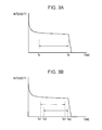
- However, even if a constant current is applied to a light source irradiating light on a biological sample, intensity of emitted light varies in accordance with a temperature of the light source itself. For example, as shown in
Fig. 1 , a halogen lamp used for a light source outputs a higher intensity immediately after starting light emission because of a low temperature of the halogen lamp itself, lowers the intensity with time as the temperature of the lamp increases, and goes into a thermal equilibrium state after passage of a predetermined time, outputting a constant intensity. - In such a case, in a microscope apparatus, intensity of light emitted from a light source varies with time, and thus even if an exposure time is kept constant, an exposure quantity on an imaging device changes for each divided image.
- As a result, for example, as shown in
Fig. 2 , in a microscope apparatus, it is difficult to keep luminance values of divided images DP at constant. Thus, in a biological sample image SP produced by connecting divided images DP, joints of the divided images DP become conspicuous. In particular, a joint between an upper and a lower divided images DP becomes more conspicuous because the images are captured at greatly different time. - Thus, as shown in
Fig. 3A , in general, in a microscope apparatus, exposure on an imaging device is started at time Ts when a light source has reaches a thermal equilibrium state after passage of a predetermined time from the light source starting light emission, and the exposure is terminated at time Te when a certain time has passed in order to capture divided images. Here, inFig. 3A , a CCD (Charge Coupled Device) sensor is used as an imaging device. In a CCD sensor, it is possible to start and end exposure for all the pixels at the same time. - Accordingly, it is possible to reduce luminance differences among a plurality of divided images using this method. However, in this method, it takes time until the light source reaches a thermal equilibrium state, and thus the imaging time period becomes disadvantageously long.
- Also, in the case of using a CMOS (Complementary Metal Oxide Semiconductor) image sensor as an imaging device, the CMOS image sensor starts and ends exposure in sequence for each line along an array of pixels, and thus, as shown in
Fig. 3B , there has been a problem in that an imaging time period becomes further long. In this regard, inFig. 3B , time Ts1 indicates exposure start time of a line on which exposure is started first, and time Ts2 indicates exposure start time of a line on which exposure is started last. Also, time Te1 indicates exposure end time of the line corresponding to time Ts1, and time Te2 indicates exposure end time of the line corresponding to time Ts2. - The present invention has been made in consideration of the above-described points. It is desirable to propose an image acquisition apparatus and method for acquiring an image, which is capable of shortening an imaging time period, and reducing luminance differences among images of small areas allocated to an imaging object.
- According to an embodiment of the present invention, there is provided an image acquisition apparatus including: an imaging device on which an image of a small area allocated to an area to be imaged is formed; a detection section detecting intensity of light irradiated on the small area from a light source; an integration section integrating the intensity of light detected by the detection section; if an integration value of the intensity of light integrated by the integration section from a point in time when light is emitted from the light source is greater than a predetermined threshold value, a light-source control section terminates emission of light from the light source; an exposure control section starting exposure of the imaging device before light is emitted from the light source and terminating exposure of the imaging device after emission of light from the light source is terminated; and an image acquisition section acquiring the image of the small area as a divided image from the imaging device.
- Also, according to another embodiment of the present invention, there is provided a method of acquiring an image, the method including the steps of: detecting intensity of light irradiated from a light source on a small area allocated to an area to be imaged; integrating the intensity of light detected by the step of detecting; if an integration value of the intensity of light integrated by the step of integrating from a point in time when light is emitted from the light source is greater than a predetermined threshold value, controlling the light source so as to terminate emission of light from the light source; controlling exposure so as to start exposure of the imaging device on which an image of the small area is formed before light is emitted from the light source and to terminate exposure of the imaging device after emission of light from the light source is terminated; and acquiring the image of the small area as a divided image from the imaging device.
- Thereby, a certain amount of light can be emitted from the light source while the imaging device is exposed so that it is possible to keep an exposure quantity of the imaging device constant when a plurality of divided images are obtained.
- Also, according to another embodiment of the present invention, there is provided an image acquisition apparatus including: an imaging device on which an image of a small area allocated to an area to be imaged is formed; a detection section detecting intensity of light irradiated on the small area from a light source; an integration section integrating the intensity of light detected by the detection section; a light-source control section emitting light from the light source such that a time interval between start and end of emission becomes constant; an exposure control section starting exposure of the imaging device before light is emitted from the light source by the light-source control section and terminating exposure of the imaging device after emission of light from the light source is terminated by the light-source control section; an image acquisition section acquiring the image of the small area as a divided image from the imaging device; a correction section correcting a luminance value of the divided image such that an integration value of intensity of light integrated by the integration section at the time when the divided image is captured becomes the same; and an image generation section generating one image by combining the divided images corrected by the correction section.
- Also, according to another embodiment of the present invention, there is provided a method of acquiring an image, the method including the steps of: detecting intensity of light irradiated from a light source on a small area allocated to an area to be imaged; integrating the intensity of light detected by the step of detecting; controlling the light source to emit light such that a time interval between start and end of emission becomes constant; controlling exposure so as to start exposure of the imaging device before light is emitted from the light source by the step of controlling the light source and terminating exposure of the imaging device after emission of light from the light source is terminated by the step of controlling the light source; acquiring the image of the small area as a divided image from the imaging device; correcting a luminance value of the divided image such that an integration value of intensity of light integrated by the step of integrating at the time when the divided image is captured becomes the same; and generating one image by combining the divided images corrected by the step of correcting.
- Thereby, the luminance values of the divided images are corrected such that the integration values of intensities of light emitted from the light source while the imaging device is exposed become the same, and thus the luminance differences among divided images can be reduced.
- As described above, by the present invention, a certain amount of light can be emitted from the light source while the imaging device is exposed so that it is possible to keep exposure quantities of the imaging device at constant when a plurality of divided images are obtained. Thereby, it is possible to achieve an image acquisition apparatus and method for acquiring an image, which is capable of shortening an imaging time period, and reducing luminance differences among images of small areas allocated to an imaging object.
- Also, by the present invention, the luminance values of the divided images are corrected such that the integration values of intensities of light emitted from the light source while the imaging device is exposed become the same so that it is possible to keep exposure quantities of the imaging device at constant when a plurality of divided images are obtained. Thereby, it is possible to achieve an image acquisition apparatus and method for acquiring an image, which is capable of shortening an imaging time period, and reducing luminance differences among images of small areas allocated to an imaging object.
-
-
Fig. 1 is a graph illustrating a change in intensity of a halogen lamp; -
Fig. 2 is a schematic diagram illustrating a related-art biological sample image; -
Fig. 3 is a graph illustrating a related-art relationship between light intensity and exposure time; -
Fig. 4 is a schematic diagram illustrating a biological-sample-image acquisition apparatus; -
Fig. 5 is a schematic diagram illustrating configurations of a light-source unit and a light-source control section according to a first embodiment; -
Fig. 6 is a graph illustrating a change in intensity of an LED; -
Fig. 7 is a schematic diagram illustrating a timing chart in controlling a light source; -
Fig. 8 is a schematic diagram illustrating a configuration of a data processing section; -
Fig. 9 is a schematic diagram illustrating a functional configuration of a CPU performing biological-sample acquisition processing according to the first embodiment; -
Fig. 10 is a schematic diagram illustrating small areas allocated to a biological sample; -
Fig. 11 is a graph illustrating a relationship between light intensity and exposure time according to the first embodiment; -
Fig. 12 is a flowchart illustrating a biological-sample-image acquisition processing procedure according to the first embodiment; -
Fig. 13 is a schematic diagram illustrating configurations of a light-source unit and a light-source control section according to a second embodiment; -
Fig. 14 is a schematic diagram illustrating a functional configuration of a CPU performing biological-sample acquisition processing according to the second embodiment; -
Fig. 15 is a flowchart illustrating a biological-sample-image acquisition processing procedure according to the second embodiment; -
Fig. 16 is a schematic diagram illustrating a functional configuration of a CPU performing biological-sample acquisition processing according to another embodiment; -
Fig. 17 is a flowchart illustrating a biological-sample-image acquisition processing procedure according to another embodiment; -
Fig. 18 is a graph illustrating a relationship (1) between light intensity and exposure time according to another embodiment; and -
Fig. 19 is a graph illustrating a relationship (2) between light intensity and exposure time according to another embodiment. - In the following, descriptions will be given of modes for carrying out the invention. In this regard, the descriptions will be given in the following order.
-
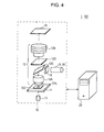
Fig. 4 illustrates a biological-sample-image acquisition apparatus 1 according to an embodiment of the present invention. The biological-sample-image acquisition apparatus 1 includes amicroscope 10 and adata processing section 20. - The
microscope 10 has a plane on which a biological sample SPL including a biomacromolecule, such as a tissue section, or a cell, or a chromosome, etc., can be placed, and has a stage (in the following, referred to as a movable stage) 11 movable in a parallel direction and in a perpendicular direction to that plane (in the x-, y-, and z-axis directions). - In this embodiment, the biological sample SPL is fixed on a microscope slide SG by a predetermined fixing method, and staining is applied to the biological sample SPL as necessary. The staining includes not only general staining as typified by HE (Hematoxylin-Eosin) staining, Giemsa stain or Papanicolaou stain, etc., but also fluorescence staining such as FISH (Fluorescence In-Situ Hybridization), an immunoenzymatic technique, etc.
- An
optical system 12 is disposed on one side of the plane of themovable stage 11 in themicroscope 10, and a light-source unit 13 is disposed on the other side of the plane of themovable stage 11. Themicroscope 10 captures an image of a biological sample SPL either in a bright-field mode or a dark-field mode by changing the modes. - In the bright-field mode, the light-
source unit 13 emits light under the control of the light-source control section 30 (Fig. 5 ), irradiates the light on the biological sample SPL disposed on one side of the plane of themovable stage 11 through an opening formed on themovable stage 11 as illumination light. - The
microscope 10 enlarges a part of an image of the biological sample SPL obtained by the illumination light by anobjective lens 12A and animaging lens 12B of theoptical system 12 at a predetermined magnification. And themicroscope 10 forms an image enlarged by theobjective lens 12A and theimaging lens 12B on an imaging surface of aCMOS image sensor 14. - In this regard, in the bright-field mode, in the
microscope 10, adichroic mirror 12C and anemission filter 12D can be removed from a light path between theobjective lens 12A and theimaging lens 12B. - Incidentally, an excitation-light-source system 15 and an
excitation filter 16 are disposed at a predetermined position of themicroscope 10. In the dark-field mode, in themicroscope 10, when an excitation-light-source system 15 emits light, excitation light, which is produced by transmitting only light having an excitation wavelength for fluorescence staining among the emitted light by theexcitation filter 16 is reflected by adichroic mirror 12C disposed between theobjective lens 12A and theimaging lens 12B, and is led to theobjective lens 12A. And, in themicroscope 10, the excitation light is focussed by theobjective lens 12A on the biological sample SPL disposed on themovable stage 11. - If fluorescence staining has been applied on the biological sample SPL fixed on the microscope slide SG, the fluorescent dye emit light by the excitation light. Light (in the following, also referred to as color development light) obtained by the emission is transmitted through the
dichroic mirror 12C via theobjective lens 12A. And the color development light reaches theimaging lens 12B through anemission filter 12D disposed between thedichroic mirror 12C and theimaging lens 12B. - The
microscope 10 enlarges an image of the color development light by theobjective lens 12A, and absorbs light other than the color development light (in the following, also referred to as the other light) by theemission filter 12D. And themicroscope 10 enlarges an image of the color development light having lost the other light by theimaging lens 12B, and forms the image on the imaging surface of theCMOS image sensor 14. - On the other hand, the
data processing section 20 generates the entire image of the biological sample SPL (in the following, also referred to as a biological sample image) using theCMOS image sensor 14, and stores the image as predetermined-format data (in the following, also referred to as sample data). - In this manner, the biological-sample-
image acquisition apparatus 1 can store a biological sample SPL disposed on the microscope slide SG as an image in a microscopic state. Accordingly, it becomes possible for the biological-sample-image acquisition apparatus 1 to store the biological sample SPL over a long period of time without deteriorating states, such as fixing, staining, etc., compared with a case of storing the microscope slide SG itself. - Next, a description will be given of the light-
source unit 13 and the light-source control section 30 controlling the light-source unit 13 usingFig. 5 . - The light-
source unit 13 has a configuration including a white LED (Light Emitting Diode) 13A outputting white light, acondenser 13B converting light emitted from thewhite LED 13A into substantially parallel light rays, and aphotodetector 13C measuring intensity of light emitted from thewhite LED 13A. - As shown in
Fig. 6 , thewhite LED 13A has a characteristic in which if a constant current is applied, the LED outputs a higher intensity immediately after starting light emission because of a low temperature of the LED itself, lowers the intensity with time as the temperature of the LED increases, and goes into a thermal equilibrium state after passage of a predetermined time, outputting a constant intensity. - When the
LED driver 35 supplies a current to thewhite LED 13A, thewhite LED 13A emits light diffused in a certain range. Thecondenser 13B converts light irradiated on itself among the diffused light emitted from thewhite LED 13A into parallel light rays, and irradiates the biological sample SPL. - The
photodetector 13C is disposed at a position where part of the diffused light emitted from thewhite LED 13A is irradiated among diffused light emitted from thewhite LED 13A without blocking a light path of light irradiated on thecondenser 13B. - And when the
photodetector 13C receives part of diffused light emitted from thewhite LED 13A, thephotodetector 13C detects the intensity of the irradiated light, and sends a light-intensity signal S1 in accordance with the light intensity to anintegrator 32. - On the other hand, the light-source control section 30 (
Fig. 5 ) includes asystem controller 31, theintegrator 32, acomparator 33, an ANDcircuit 34, and anLED driver 35. - The
system controller 31 has a computer configuration including a CPU, a ROM storing various programs, etc., and a RAM functioning as a work memory of the CPU, and totally controlsindividual sections 31 to 35 of the light-source control section 30. - When the
data processing section 20 supplies an electronic flash instruction SS to the light-source control section 30, the light-source control section 30 controls light aimed at the biological sample SPL in accordance with a timing chart shown inFig. 7 . - Specifically, when the
data processing section 20 supplies the electronic flash instruction SS to thesystem controller 31, thesystem controller 31 sends a reset signal S2 to theintegrator 32. - Also, the
system controller 31 sends a threshold-value signal S4 indicating a predetermined threshold value to thecomparator 33. - Further, the
system controller 31 outputs a light-emission instruction S6 for instructing thewhite LED 13A to output light to the ANDcircuit 34. The light-emission instruction S6 is output for a time period longer than a time period while thewhite LED 13A should output light, and shorter than a time period at which the next reset signal S2 is output. - When the
integrator 32 receives the reset signal S2, theintegrator 32 resets an integration value having been integrated up to that time in response to the reset signal S2. And theintegrator 32 starts integrating the light intensity in accordance with the light-intensity signal S1 supplied from thephotodetector 13C from a point in time of the reset, and sends an integration-value signal S3 indicating the integration value to thecomparator 33. - The
comparator 33 compares a threshold value indicated by a threshold-value signal S4 supplied from thesystem controller 31 and an integration value indicated by an integration-value signal S3 supplied from theintegrator 32. If the integration value is less than the threshold value, thecomparator 33 sends an output signal S5, which causes thewhite LED 13A to output light, to the ANDcircuit 34. If the integration value is not less than the threshold value, thecomparator 33 does not send an output signal S5, which causes thewhite LED 13A to output light, to the ANDcircuit 34. - If the AND
circuit 34 is supplied with an output signal S5 from thecomparator 33, and a light-emission instruction signal S6 from thesystem controller 31, the ANDcircuit 34 sends a light-emission instruction signal S7 for causing thewhite LED 13A to emit light to theLED driver 35. - If the AND
circuit 34 supplies theLED driver 35 with a light-emission instruction signal S7, theLED driver 35 applies a constant current to thewhite LED 13A so that thewhite LED 13A emits light. - In this manner, when the light-source control section 30 is supplied with an electronic flash instruction SS from the
data processing section 20, the light-source control section 30 controls thewhite LED 13A to emit light until the integration value of the intensity of light measured by thephotodetector 13C reaches the threshold value. - And the light-source control section 30 stops the current to be supplied to the
white LED 13A in order to cause thewhite LED 13A to stop light emission at a point in time when the integration value of the intensity of light measured by thephotodetector 13C has reached the threshold value. - Thereby, it is possible for the light-source control section 30 to keep the light quantity emitted from the
white LED 13A onto theCMOS image sensor 14 through thecondenser 13B for each time the electronic flash instruction SS is supplied from thedata processing section 20. - Incidentally, the
system controller 31 is allowed to obtain the light-emission instruction signal S7 output from the ANDcircuit 34, and to output a light-emission-end signal indicating that supplying electricity to thewhite LED 13A has ended to thedata processing section 20 on the basis of the light-emission instruction signal S7. - Next, a description will be given of a configuration of the
data processing section 20. As shown inFig. 8 , thedata processing section 20 has a configuration in which various kinds of hardware are connected to a CPU (Central Processing Unit) 21 performing control. - Specifically, a ROM (Read Only Memory) 22, a RAM(Random Access Memory) 23 to be a work memory for the
CPU 21, anoperation input section 24 to which an instruction in accordance with a user's operation is input, aninterface section 25, adisplay section 26, and astorage section 27 are connected through abus 28. - The
ROM 22 stores programs for executing various kinds of processing. The microscope 10 (Fig. 4 ) is connected to theinterface section 25. - A liquid-crystal display, or an EL (Electro Luminescence) display or a plasma display, etc., is employed for the
display section 26. Also, a magnetic disk typified by a (Hard Disk), or a semiconductor memory, or an optical disc, etc., is employed for thestorage section 27. A portable memory, such as a USB (Universal Serial Bus) memory, or a CF (Compact Flash) memory, etc., may be employed. - The
CPU 21 loads a program corresponding to an instruction given from theoperation input section 23 among a plurality of programs stored in theROM 22 into theRAM 23, and suitably controls thedisplay section 26 and thestorage section 27 in accordance with the loaded program. Also, theCPU 21 suitably controls individual sections of themicroscope 10 through theinterface section 25. - When the
CPU 21 receives an acquisition instruction of an image of a biological sample SPL from theoperation input section 24, theCPU 21 loads a program corresponding to the obtained instruction into theRAM 23. - As shown in
Fig. 9 , theCPU 21 functions as amovement control section 41, anexposure control section 42, an electronic-flash control section 43, animage acquisition section 44, animage generation section 45, and adata recording section 46 in accordance with the program corresponding to the acquisition instruction of the image of the biological sample SPL. - For example, as shown in
Fig. 10 , themovement control section 41 allocates an area of a biological sample SPL to be imaged (in the following, also referred to as a sample area) PR to a plurality of small areas AR to match magnifications of theobjective lens 12A and theimaging lens 12B. In this regard, inFig. 10 , small areas AR are not overlapped one another. However, part of adjacent areas may be overlapped. - And the
movement control section 41 moves themovable stage 11 such that an area to be imaged by theCMOS image sensor 14 becomes, for example, a small area AR on the upper-left corner among a plurality of small areas AR. - After the
movement control section 41 performed movement so that the upper-left small area AR became an area to be imaged, theexposure control section 42 starts theCMOS image sensor 14 to be exposed. - After the
exposure control section 42 started the exposure of theCMOS image sensor 14, preferably at a point in time when the exposure is started, the electronic-flash control section 43 outputs the electronic flash instruction SS to the light-source control section 30. When the electronic flash instruction SS is supplied by the electronic-flash control section 43, the light-source control section 30 causes thewhite LED 13A to emit a certain amount of light as described above. - After the electronic-
flash control section 43 outputs the electronic flash instruction SS, and thesystem controller 31 supplied the light-emission-end signal, preferably at a point in time when a light-emission-end signal is supplied, theexposure control section 42 stops the exposure of theCMOS image sensor 14. - The
image acquisition section 44 reads out an electronic signal of each pixel of theCMOS image sensor 14 in sequence for each scanning line, and obtains an image of the biological-sample SPL member of the small area AR obtained as a result as a divided image. - Accordingly, as shown in
Fig. 11 , after exposure of all the pixels of theCMOS image sensor 14 has been started, theexposure control section 42 and the electronic-flash control section 43 cause thewhite LED 13A to emit light. And after theexposure control section 42 and the electronic-flash control section 43 have caused thewhite LED 13A to emit a certain amount of light, theexposure control section 42 and the electronic-flash control section 43 terminate the exposure of all the pixels of theCMOS image sensor 14. - In this regard, in
Fig. 11 , time Ts3 indicates exposure start time of a scanning line on which exposure is started first, and time Ts4 indicates exposure start time of a scanning line on which exposure is started last. Also, time Te3 indicates exposure end time of the scanning line corresponding to time Ts3, and time Te4 indicates exposure end time of the scanning line corresponding to time Ts4. - The
movement control section 41 causes theimage acquisition section 44 to read out an electronic signal of theCMOS image sensor 14, and at the same time, moves themovable stage 11 such that the next area to be imaged by theCMOS image sensor 14 becomes, for example, a small area AR on the right of the upper-left small area AR. - The
exposure control section 42 and the electronic-flash control section 43 cause theCMOS image sensor 14 to start being exposed, and outputs the electronic flash instruction SS to the light-source control section 30 to cause thewhite LED 13A to emit a certain amount of light. After that, theexposure control section 42 and the electronic-flash control section 43 ends the exposure of theCMOS image sensor 14. Also, theimage acquisition section 44 obtains the divided images from theCMOS image sensor 14. - In this manner, the
movement control section 41 moves an area to be imaged by theCMOS image sensor 14 in sequence from a small area AR of the uppermost left end to that of the right end. Next, themovement control section 41 moves downward by one row, and moves in sequence from the right end to the left end. In this manner, themovement control section 41 moves the area to be imaged in the opposite direction alternately for each row until the divided images corresponding to all the small areas AR are obtained. - And the
exposure control section 42, the electronic-flash control section 43, and theimage acquisition section 44 function in the same manner as described above, and obtain the divided image in the small area AR each time the area to be imaged is moved to one of the small areas AR by themovement control section 41. - The
image generation section 45 combines a plurality of divided images obtained by theimage acquisition section 44 to generate a biological sample image. - When the biological sample image is generated, the
data recording section 46 generates sample data including image information indicating the entire biological sample image or a part of the image that can restore the biological sample image. - And the
data recording section 46 adds data indicating identification information on the biological sample image to the sample data, and records the sample data with that data into thestorage section 27. - The identification information includes information such as, an examinee name, an examinee gender, an examinee age, and an acquisition date, etc., of the biological sample SPL, for example. The
data recording section 46 informs that the identification information should be input at predetermined timing, such as at the timing when a data storage instruction of the biological sample SPL is given, at the timing when the microscope slide SG should be set, etc. - Also, if identification information has not been obtained at the time when biological sample data is created, the
data recording section 46 gives a warning that the identification information should be input. In this regard, a notification or a warning that the identification information should be input is given, for example, by sound or through a GUI (Graphical User Interface) screen, etc. - Next, a description will be given the above-described biological-sample-image acquisition processing procedure in accordance with a flowchart shown in
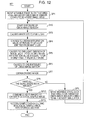
Fig. 12 . - Actually, the
CPU 21 enters a routine RT1 from a start step, and proceeds to the next step SP1. In step SP1, theCPU 21 allocates a sample area PR to a plurality of small areas AR, and moves themovable stage 11 such that an area to be imaged by theCMOS image sensor 14 is a first (upper left) small area AR, and the processing proceeds to the next step SP2. - In step SP2, the
CPU 21 starts exposure of theCMOS image sensor 14, and the processing proceeds to the next step SP3. - In step SP3, the
CPU 21 outputs an electronic flash instruction SS to the light-source control section 30 to cause thewhite LED 13A to emit light, then in the next step SP4, obtains an integration value of the intensity of light emitted from thewhite LED 13A, and the processing proceeds to the next step SP5. - In step SP5, at the point in time when the integration value becomes a threshold value or higher, the
CPU 21 causes the light-source control section 30 to end light emission from thewhite LED 13A, and the processing proceeds to the next step SP6. - In step SP6, the
CPU 21 ends the exposure on theCMOS image sensor 14, and processing proceeds to the next step SP7. - In step SP7, the
CPU 21 reads out an electronic signal of each pixel of theCMOS image sensor 14 in sequence for each line, obtains a divided image as a result, and the processing proceeds to the next step SP8. - In step SP8, the
CPU 21 determines whether all the small areas AR have been imaged. If a negative result is obtained, it means that there is a small area AR yet to be imaged, and thus the processing proceeds to the next step SP9. - In step SP9, the
CPU 21 moves themovable stage 11 such that an area to be imaged by theCMOS image sensor 14 becomes the next small area AR, and the processing returns to step SP2. - The
CPU 21 repeats from step SP2 to step SP9 until an affirmative result is obtained in step SP8. When the affirmative result is obtained, it means that divided images corresponding to all the small areas AR have been obtained, and the processing proceeds to step SP10. - In step SP10, the
CPU 21 combines the divided images to generate a biological sample image, then in the next step SP11, stores the sample data including the biological sample image into thestorage section 27, and the processing proceeds to the next step to end the processing. - In the above-described configuration of the biological-sample-
image acquisition apparatus 1, light from thewhite LED 13A is irradiated on small areas AR individually allocated to sample area PR including a biological sample SPL to be imaged. - In the biological-sample-
image acquisition apparatus 1, thephotodetector 13C detects intensity of light emitted from thewhite LED 13A, the light intensity is integrated by theintegrator 32, and light emission from thewhite LED 13A is ended at the time when the integration value becomes a threshold value or higher. - In the biological-sample-
image acquisition apparatus 1, exposure on theCMOS image sensor 14 is started before thewhite LED 13A emits light, and exposure on theCMOS image sensor 14 is ended after light emission from thewhite LED 13A is ended. - And in the biological-sample-
image acquisition apparatus 1, an image of a small area AR is obtained from theCMOS image sensor 14 as a divided image. - Thereby, in the biological-sample-
image acquisition apparatus 1, when all the divided images are individually obtained, the amount of light emitted from thewhite LED 13A can be kept constant. Thus, it is possible to keep an exposure quantity on theCMOS image sensor 14 constant when each of the small areas AR is imaged. - Accordingly, in the biological-sample-
image acquisition apparatus 1, when divided images of all the small area AR are obtained, and these divided images are combined into one piece of a biological sample image, even if the intensity of light of thewhite LED 13A varies, luminance differences among all the divided images can be reduced. - Also, in the biological-sample-
image acquisition apparatus 1, it is not necessary to start imaging after thewhite LED 13A goes into a thermal equilibrium state, and thus the imaging period can be shortened by that amount of time. - Incidentally, in the case of employing an imaging device which performs starting exposure, ending exposure, and reading out an electronic signal for each line, such as a
CMOS image sensor 14, a time difference arises for each line in starting exposure, ending exposure, and reading out the electronic signal. - However, in the biological-sample-
image acquisition apparatus 1, exposure of all the pixels of theCMOS image sensor 14 is started before thewhite LED 13A emits light, and exposure of all the pixels of theCMOS image sensor 14 is ended after thewhite LED 13A has ended light emission. - Thereby, in the biological-sample-
image acquisition apparatus 1, in the case of employing an imaging device which performs starting exposure, ending exposure, and reading out an electronic signal for each line, such as aCMOS image sensor 14, it is possible to obtain divided images without having luminance difference for each line. - Incidentally, in the biological-sample-
image acquisition apparatus 1, a method is considered in which thewhite LED 13A emits light all the time, and exposure quantity of theCMOS image sensor 14 is kept constant by opening and closing a mechanical shutter disposed on a light path of the light. - In this method, in general, since a life span of a mechanical shutter is from 100 thousand times to one million times, if this method is employed in the biological-sample-
image acquisition apparatus 1 capturing hundreds of divided images in one minute, the mechanical shutter reaches the life span in about three days. - In contrast, in the biological-sample-
image acquisition apparatus 1, exposure quantity of theCMOS image sensor 14 is kept constant by the emission control of thewhite LED 13A, and thus it is more advantageous in maintainability and in economical efficiency than the case of disposing a mechanical shutter. - Also, for another method, a method is considered in which the
white LED 13A is controlled at a constant intensity by so-called APC (Auto Power Control) in order to keep the exposure quantity of theCMOS image sensor 14 constant. - By this method, it is possible to keep the light intensity constant in a shorter time than the time period in which the
white LED 13A goes into a thermal equilibrium state. However, it is necessary to design a control band to be a high band so that the APC can sufficiently respond in an electronic-flash emission time in this method. In particular, in the case of using an LED driver having a high-efficiency output format, such as a PWM (Pulse Width Modulation) method, etc., a control band of an LED current is restricted by a PWM carrier frequency, and thus it is difficult to achieve APC having a high response speed. - In contrast, in the biological-sample-
image acquisition apparatus 1, the amount of light emitted from thewhite LED 13A is kept constant. Accordingly, it is not necessary to wait for intensity of light emitted from thewhite LED 13A to become constant, and the imaging period can be shortened by that period. Also, even if an LED current pulsates by the PWM method, the amount of light can be correctly kept constant. - With the above arrangement, in the biological-sample-
image acquisition apparatus 1, exposure of theCMOS image sensor 14 on a small area AR allocated on a sample area PR is started before thewhite LED 13A emits light. Also, in the biological-sample-image acquisition apparatus 1, exposure of theCMOS image sensor 14 is ended to obtain a divided image after thewhite LED 13A has emitted a certain amount of light. - Thereby, in the biological-sample-
image acquisition apparatus 1, it is possible to keep the exposure quantity of theCMOS image sensor 14 constant without waiting for thewhite LED 13A to go into a thermal equilibrium state. Thus, it is possible to shorten an imaging period, and to reduce luminance differences among the divided images. - In a second embodiment, the functional configurations of the light-source control section and the CPU are different from those of the first embodiment. In this regard, the configurations of the biological-sample-
image acquisition apparatus 1 and thedata processing section 20 are the same as those of the first embodiment, and the descriptions thereof will be omitted. - As shown in
Fig. 13 , in which the same reference letters and numerals are given as the corresponding parts ofFig. 5 , a light-source control section 60 includes asystem controller 31, anintegrator 32, and anLED driver 35. Thesystem controller 31 suitably controls theintegrator 32 and theLED driver 35. - When the
LED driver 35 supplies a current to thewhite LED 13A, thewhite LED 13A emits light diffused in a certain range. When part of diffused light emitted from thewhite LED 13A is irradiated on thephotodetector 13C, thephotodetector 13C measures the intensity of the irradiated light, and sends the light-intensity signal S1 in accordance with the light intensity to theintegrator 32. - When the
data processing section 20 supplies the electronic flash instruction SS to thesystem controller 31, thesystem controller 31 sends the reset signal S2 to theintegrator 32. - When the
integrator 32 receives the reset signal S2, theintegrator 32 resets an integration value having been integrated up to that time in response to the reset signal S2. And theintegrator 32 integrates the light intensity in accordance with the light-intensity signal S1 supplied from thephotodetector 13C from a point in time of the reset. - After the
system controller 31 sends the reset signal S2 to theintegrator 32, thesystem controller 31 outputs a light-emission instruction signal S11 for causing thewhite LED 13A to emit light to theLED driver 35 during a certain time period set to be a same interval all the time from an emission start to an emission end. - When the
system controller 31 supplies theLED driver 35 with the light-emission instruction signal S11, theLED driver 35 applies a constant current to thewhite LED 13A for a certain time period so that thewhite LED 13A emits light for a certain time period. - The
integrator 32 integrates the intensity of light emitted from thewhite LED 13A for a certain time period from a point in time of reset, and sends an integration-value signal S3 indicating the integration value obtained as a result to thesystem controller 31. - In this manner, when the light-source control section 30 is supplied with an electronic flash instruction SS from the
data processing section 20, the light-source control section controls thewhite LED 13A to emit light for a certain time period, and the light-source control section 30 obtains the integration value of the intensity of light emitted from the white LED 31A during that time. - When the
CPU 21 receives an acquisition instruction of an image of a biological sample SPL from theoperation input section 24, theCPU 21 loads a program corresponding to the obtained instruction into theRAM 23. - As shown in
Fig. 14 , theCPU 21 functions as themovement control section 41, theexposure control section 42, the electronic-flash control section 43, theimage acquisition section 44, theimage correction section 47, theimage generation section 45, and thedata recording section 46 in accordance with the program corresponding to the acquisition instruction of the image of the biological sample SPL. - The
movement control section 41 allocates a sample area PR to a plurality of small areas AR, and moves themovable stage 11 such that an area to be imaged by theCMOS image sensor 14 becomes, for example, a small area AR on the upper-left corner among a plurality of small areas AR. - After the
movement control section 41 performed movement so that the upper-left small area AR became an area to be imaged, theexposure control section 42 starts theCMOS image sensor 14 to be exposed. - After the
exposure control section 42 started the exposure of theCMOS image sensor 14, preferably at a point in time when the exposure of theCMOS image sensor 14 is started, the electronic-flash control section 43 outputs the flash instruction SS to the light-source control section 60. When the electronic flash instruction SS is supplied by the electronic-flash control section 43, the light-source control section 60 causes thewhite LED 13A to emit light for a certain time period. - After the light emission from the
white LED 13A is ended by the light-source control section 60, theexposure control section 42 ends exposure of theCMOS image sensor 14 preferably at a point in time when light emission is ended. - The
image acquisition section 44 reads out an electronic signal of each pixel of theCMOS image sensor 14 in sequence for each line, and obtains an image of the biological-sample SPL member of the upper-left small area AR obtained as a result as a divided image. - At this time image, when the
acquisition section 44 obtains the divided image of the upper-left small area AR, theacquisition section 44 obtains the integration-value signal S3 indicating the integration value of the intensity of the light irradiated by thewhite LED 13A for a certain time period. - When a divided image is obtained, the
movement control section 41 moves themovable stage 11 to the next small area AR. And theexposure control section 42, the electronic-flash control section 43, and theimage acquisition section 44 obtain a divided image and an integration-value signal S3 of the small area AR by functioning in the same manner as described above each time themovement control section 41 moves themovable stage 11 to any small area AR. - The
image correction section 47 calculates a magnification for matching the integration value indicated by the integration-value signal S3 with a predetermined value, and multiplies the calculated magnification and the luminance value of the divided image corresponding to the integration value so as to correct the luminance value of the divided image. - The
image correction section 47 corrects the luminance values for all the divided images in the same manner. Also, theimage correction section 47 performs distortion correction that corrects distortions of all the divided images. - The
image generation section 45 combines the divided images corrected by theimage correction section 47 to generate a biological sample image. When the biological sample image is generated, thedata recording section 46 generates sample data including image information indicating the entire biological sample image or a part of the image that can restore the biological sample image. - Next, a description will be given the above-described biological-sample-image acquisition processing procedure in accordance with a flowchart shown in
Fig. 15 . - Actually, the
CPU 21 enters a routine RT2 from a start step, and proceeds to the next step SP21. In step SP21, theCPU 21 allocates a sample area PR to a plurality of small areas AR, and moves themovable stage 11 such that an area to be imaged by theCMOS image sensor 14 is a first imaging area AR, and the processing proceeds to the next step SP22. - In step SP22, the
CPU 21 starts exposure of theCMOS image sensor 14, and the processing proceeds to the next step SP23. - In step SP23, the
CPU 21 outputs an electronic flash instruction SS to the light-source control section 60 to cause thewhite LED 13A to emit light for a certain time period and by a constant current, and the processing proceeds to the next step SP24. - In step SP24, the
CPU 21 ends the exposure on theCMOS image sensor 14, and processing proceeds to the next step SP25. - In step SP25, the
CPU 21 reads out an electronic signal of each pixel of theCMOS image sensor 14 in sequence for each line, obtains a divided image as a result, also obtains an integration value signal S3 corresponding to the divided image, and the processing proceeds to the next step SP26. - In step SP26, the
CPU 21 determines whether all the small areas AR have been imaged. If a negative result is obtained, it means that there is a small area AR yet to be imaged, and thus the processing proceeds to the next step SP27. - In step SP27, the
CPU 21 moves themovable stage 11 such that an area to be imaged by theCMOS image sensor 14 becomes the next small area AR, and the processing returns to step SP22. - The
CPU 21 repeats from step SP22 to step SP27 until an affirmative result is obtained in step SP26. When the affirmative is obtained, it means that divided images and the integration value signals S3, which correspond to all the small areas AR, have been obtained, and the processing proceeds to step SP28. - In step SP28, the
CPU 21 calculates magnifications for matching the integration values indicated by the integration-value signals S3 individually corresponding to all the divided images with a predetermined value set in advance, multiplies the magnifications and the luminance values of the divided images so as to correct the luminance values of the divided images, respectively, and the processing proceeds to the next step SP29. - In step SP29, the
CPU 21 performs distortion correction on the divided images having been subjected to the luminance-value correction. In the next step SP30, theCPU 21 combines the divided images into a biological sample image, and the processing proceeds to the next step SP31. - In step SP31, the
CPU 21 stores the sample data including the biological sample image into thestorage section 27, and the processing proceeds to the next step to end the processing. - In the above-described configuration of the biological-sample-
image acquisition apparatus 1, light from thewhite LED 13A is irradiated for a certain time period on small areas AR individually allocated to sample area PR including a biological sample SPL to be imaged. - In the biological-sample-
image acquisition apparatus 1, thephotodetector 13C detects intensity of light emitted from thewhite LED 13A, and the light intensity is integrated by theintegrator 32 from a point in time when light is emitted. - In the biological-sample-
image acquisition apparatus 1, exposure on theCMOS image sensor 14 is started before thewhite LED 13A emits light, and exposure on theCMOS image sensor 14 is ended after light emission from thewhite LED 13A is ended. - And in the biological-sample-
image acquisition apparatus 1, an image of a small area AR is obtained from theCMOS image sensor 14 as a divided image, and an integration value corresponding to each of the divided images is obtained. - And in the biological-sample-
image acquisition apparatus 1, luminance values of the divided images are corrected so that the integration values become constant, and the corrected divided images are combined into a biological sample image. - Thereby, in the biological-sample-
image acquisition apparatus 1, it is possible to keep exposure time of theCMOS image sensor 14 constant when a small area AR is imaged, and to correct the luminance value of a divided image using the integration value corresponding to the exposure quantity at that time. Thus, it is possible to reduce the luminance differences among the divided images. - Also, in the biological-sample-
image acquisition apparatus 1, it is not necessary to start imaging after thewhite LED 13A goes into a thermal equilibrium state, and thus the imaging period can be shortened by that amount of time. - Further, in the biological-sample-
image acquisition apparatus 1, even in the case of employing an imaging device which performs starting exposure, ending exposure, and reading out an electronic signal for each line, such as aCMOS image sensor 14, it is possible to obtain divided images without having a difference in the luminance value for each line. - Also, in the biological-sample-
image acquisition apparatus 1, light emission time from thewhite LED 13A is kept constant, and thus it is possible to keep the emission time of thewhite LED 13A and the exposure time of theCMOS image sensor 14 constant all the time. - Accordingly, in the biological-sample-
image acquisition apparatus 1, the timings of the movement control of themovable stage 11, the emission control of thewhite LED 13A, and the exposure control of theCMOS image sensor 14 are not changed for each small area AR compared with controlling the exposure quantity at a certain amount as in the case of the first embodiment. Thus, in the biological-sample-image acquisition apparatus 1, the timings for the movement control, the emission control, and the exposure control can be made easily. - Incidentally, as a method for correcting the luminance values, a method is considered in which the average values of the luminance values of a plurality of divided images are individually calculated, and the luminance values of the plurality of divided images are corrected so that the average values become the same. However, by this method, the average values of the luminance values of all the divided images become the same.
- Accordingly, by this method, there are cases where it is difficult to correct the luminance value in the same manner as the case of capturing a plurality of divided images with the same exposure quantity. For example, there are cases where the luminance values become the same as to a part including a biological sample SPL and as to a part not including the biological sample SPL, etc. Accordingly, by this method, there arises a problem in which joints of the divided images DP become conspicuous.
- In contrast, in the biological-sample-
image acquisition apparatus 1, the luminance values of the divided image are corrected so that the integration values become constant. Accordingly, it is possible to correct the luminance value in the same manner as the case of capturing a plurality of divided images with the same exposure quantity, and thus joints of the divided images become inconspicuous. - With the above arrangement, in the biological-sample-
image acquisition apparatus 1, exposure of theCMOS image sensor 14 on a small area AR allocated on a sample area PR is started before thewhite LED 13A emits light. Also, in the biological-sample-image acquisition apparatus 1, exposure of theCMOS image sensor 14 is ended to obtain a divided image after thewhite LED 13A has emitted light for a certain time period. - And in the biological-sample-
image acquisition apparatus 1, the luminance values of the divided images are corrected such that the integration value of the intensities of light emitted from thewhite LED 13A become the same, and then the divided images are combined into a biological sample image. Thereby, it is possible for the biological-sample-image acquisition apparatus 1 to shorten the imaging time period, and to reduce the luminance differences among the divided images. - In this regard, in the above-described first embodiment, a description has been given of the case where the amount of light emitted from the light-
source unit 13, in the bright-field mode, onto all the small areas AR is made constant. However, the present invention is not limited to this, and the amount of excitation light emitted in the dark-field mode may be made constant. - In this case, the biological-sample-image acquisition apparatus in the dark-field mode is provided with a photodetector measuring the intensity of excitation light emitted from a excitation-light-source system, and a light-source control section receiving the light-intensity signal sent from the photodetector and controlling the excitation-light-source system.
- Also, the excitation-light-source system may include a case of disposing one excitation light source emitting excitation light having a plurality of wavelengths, or a case of disposing a plurality of excitation light sources each of which emits one excitation wavelength.
- For one example, a description will be given of the case of disposing a plurality of excitation light sources. The biological-sample-image acquisition apparatus 100 (
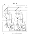
Fig. 4 ) is provided with, for example, an excitation-light-source system 80 and a light-source-control section 90 as shown inFig. 16 in place of the excitation-light source system 15 and the light-source control section 30. In this regard, in this case, it is assumed that a biological sample SPL has been subjected to fluorescence staining. - The excitation-light-
source system 80 includes light-source units mirror 83, and adichroic mirror 84. The light-source units light source LEDs condensers photodetectors 81C and 82C, respectively. - The light-
source control section 90 includes asystem controller 91, anintegrator 92, acomparator 93, an ANDcircuit 94, anLED driver 95, anintegrator 96, acomparator 97, an ANDcircuit 98, and anLED driver 99. Thesystem controller 91 totally controlsindividual sections 91 to 99 of the light-source control section 90. - When the
LED driver 95 supplies a current to the excitation-light source LED 81A, the excitation-light source LED 81A emits light diffused in a certain range. Thecondenser 81B converts light irradiated on itself among the diffused light emitted from the excitation-light source LED 81A into parallel light rays, and the parallel light is reflected on a reflectingmirror 83. The light reflected from the reflectingmirror 83 is transmitted through adichroic mirror 84, and is irradiated on the biological sample SPL through theexcitation filter 16, thedichroic mirror 12C, and theobjective lens 12A. - When the
LED driver 99 supplies a current to the excitation-light source LED 82A, the excitation-light source LED 82A emits light diffused in a certain range. Thecondenser 82B converts light irradiated on itself among the diffused light emitted from the excitation-light source LED 82A into parallel light rays, and the parallel light is reflected on adichroic mirror 84. The light reflected from thedichroic mirror 84 is irradiated on the biological sample SPL through theexcitation filter 16, thedichroic mirror 12C, and theobjective lens 12A. - When the
photodetectors 81C and 82C receive part of diffused light emitted from the excitation-light source LEDs photodetectors 81C and 82C detect the intensities of the irradiated light, and send light-intensity signals S21 and S31 in accordance with the light intensities to theintegrators integrator - When the
data processing section 20 supplies an electronic flash instruction SS to thesystem controller 91, thesystem controller 91 sends reset signals S22 and S32 to theintegrators system controller 91 sends threshold-value signals S24 and S34 indicating predetermined threshold values to thecomparators - Further, the
system controller 91 sends reset signals S22 and S32 to theintegrators light source LEDs light source LEDs - When the
integrator 92 receives the reset signal S22, theintegrator 92 resets an integration value, theintegrator 92 starts integrating the light intensity in accordance with the light-intensity signal S21 supplied from the photodetector 81C from a point in time of the reset, and sends an integration-value signal S23 indicating the integration value to thecomparator 93. - The
comparator 93 compares a threshold value indicated by a threshold-value signal S24 and an integration value indicated by an integration-value signal S23. If the integration value is less than the threshold value, thecomparator 93 sends an output signal S25, which causes the excitationlight source LED 81A to output light, to the ANDcircuit 94. - If the AND
circuit 94 is supplied with an output signal S25 from thecomparator 93, and a light-emission instruction signal S26 from thesystem controller 91, the ANDcircuit 94 sends a light-emission instruction signal S27 for causing the excitationlight source LED 81A to emit light to theLED driver 95. - If the AND
circuit 94 supplies theLED driver 95 with a light-emission instruction signal S27, theLED driver 95 applies a constant current to the excitationlight source LED 81A so that the excitationlight source LED 81A emits light. - On the other hand, when the
integrator 96 receives the reset signal S32, theintegrator 96 resets an integration value, theintegrator 96 starts integrating the light intensity in accordance with the light-intensity signal S31 supplied from thephotodetector 82C from a point in time of the reset, and sends an integration-value signal S33 indicating the integration value to thecomparator 97. - The
comparator 97 compares a threshold value indicated by a threshold-value signal S34 and an integration value indicated by an integration-value signal S33. If the integration value is less than the threshold value, thecomparator 97 sends an output signal S35, which causes the excitationlight source LED 82A to output light, to the ANDcircuit 98. - If the AND
circuit 98 is supplied with an output signal S35 from thecomparator 97, and a light-emission instruction signal S36 from thesystem controller 91, the ANDcircuit 98 sends a light-emission instruction signal S37 for causing the excitationlight source LED 82A to emit light to theLED driver 98. - If the AND
circuit 97 supplies theLED driver 99 with a light-emission instruction signal S37, theLED driver 99 applies a constant current to the excitationlight source LED 82A so that the excitationlight source LED 82A emits light. - When the
CPU 21 receives an acquisition instruction of an image of a biological sample SPL from theoperation input section 24, theCPU 21 loads a program corresponding to the obtained instruction into theRAM 23, and performs processing in accordance with a flowchart shown inFig. 17 . - Actually, the
CPU 21 enters a routine RT3 from a start step, and proceeds to the next step SP41. In step SP41, theCPU 21 allocates a sample area PR to a plurality of small areas AR, and moves themovable stage 11 such that an area to be imaged by theCMOS image sensor 14 is a first area AR to be imaged, and the processing proceeds to the next step SP42. - In step SP42, the
CPU 21 starts exposure of theCMOS image sensor 14, and the processing proceeds to the next step SP43. - In step SP43, the
CPU 21 outputs an electronic flash instruction SS to the light-source control section 90 to cause the excitationlight source LEDs - In step SP44, the
CPU 21 causes the light-source control section 90 to obtain integration values of the intensities of light emitted from the excitationlight source LEDs - In step SP45, at the point in time when the integration values become threshold values or higher, the
CPU 21 causes the light-source control section 90 to end light emission in sequence from the excitationlight source LEDs - In step SP46, after all the excitation
light source LEDs CPU 21 ends the exposure on theCMOS image sensor 14, and processing proceeds to the next step SP47. - In step SP47, the
CPU 21 reads out an electronic signal of each pixel of theCMOS image sensor 14 in sequence for each line, obtains a divided image as a result, and the processing proceeds to the next step SP48. - In step SP48, the
CPU 21 determines whether all the small areas AR have been imaged. If a negative result is obtained, it means that there is a small area AR yet to be imaged, and thus the processing proceeds to the next step SP49. - In step SP49, the
CPU 21 moves themovable stage 11 such that an area to be imaged by theCMOS image sensor 14 becomes the next small area AR, and the processing returns to step SP42. - The
CPU 21 repeats from step SP42 to step SP49 until an affirmative result is obtained in step SP48. When the affirmative is obtained, it means that divided images corresponding to all the small areas AR have been obtained, and the processing proceeds to step SP50. - In step SP50, the
CPU 21 combines the divided images into a biological sample image, then in the next step SP51, stores the sample data including the biological sample image into thestorage section 27, and the processing proceeds to the next step to end the processing. - In this manner, as shown in
Fig. 18 , in the biological-sample-image acquisition apparatus 100, before the excitationlight source LEDs CMOS image sensor 14 is started. And in the biological-sample-image acquisition apparatus 100, after both of the excitationlight source LEDs CMOS image sensor 14 is ended. - In this regard, in
Fig. 18 , time Ts5 indicates exposure start time of a line on which exposure is started first, and time Ts6 indicates exposure start time of a line on which exposure is started last. Also, time Te5 indicates exposure end time of the line corresponding to time Ts5, and time Te6 indicates exposure end time of the scanning line corresponding to time Ts6. Also, inFig. 18 , a solid line and a dash-single-dot line indicate light intensities emitted from different excitationlight source LEDs - Thereby, in the biological-sample-image acquisition apparatus 100, in the case where a plurality of excitation light source LEDs are disposed, it is possible for the excitation light source LEDs to emit light having a constant amount of light with individual wavelengths.
- Also, in the biological-sample-image acquisition apparatus 100, it is possible to keep the exposure quantity of the
CMOS image sensor 14 constant without waiting for the excitation light source LED to go into a thermal equilibrium state. Thus, it is possible to shorten an imaging period, and to reduce luminance differences in the biological sample image. - Also, in the biological sample image acquisition apparatus 100, the biological sample SPL is not kept on being exposed to the excitation light as in the case of waiting until the excitation light source LED goes into a thermal equilibrium state, and thus it is possible to restrain color fading of the fluorescent dye stained on the biological sample SPL.
- Also, in the above-described second embodiment, a description has been given of the case where the light emission time from the light-
source unit 13, in the bright-field mode, onto all the small areas AR is made constant. However, the present invention is not limited to this, and the emission time of excitation light, in the dark-field mode, onto all the small areas AR may be made constant. - Further, in the above-described first and second embodiments, a description has been given of the case of using an LED as a light source. However, the present invention is not limited, and a mercury lamp or a halogen lamp may be used as a light source.
- Further, in the above-described first and second embodiments, a description has been given of the case where a
CMOS image sensor 14 is used as an imaging device. The present invention is not limited to this, and a CCD may be used as an imaging device. - If a CCD is employed in place of the
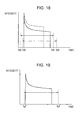
CMOS image sensor 14 in the first embodiment, as shown inFig. 19 , exposure of the CCD is started before thewhite LED 13A emits light, and exposure of the CCD ends after thewhite LED 13A has ended light emission. Thereby, even in the case of employing a CCD, it is possible to shorten an imaging period, and to reduce luminance differences among the divided images. In this regard, inFig. 19 , time Ts7 indicates exposure start time, and time Te7 indicates exposure end time. - Further, in the above-described first embodiment, a description has been given of the case where exposure of the
CMOS image sensor 14 ends after thewhite LED 13A has ended light emission. The present invention is not limited to this. If an emission time period, for which the amount of light emitted from thewhite LED 13A becomes constant, is given, an exposure time which is further longer than the emission time is set, and theCMOS image sensor 14 may be exposed for the exposure time. - Specifically, if the emission time period, for which the amount of light emitted from the
white LED 13A becomes constant, is given as a value, for example, between 30 [ms] and 50 [ms], the exposure time for which all the lines of theCMOS image sensor 14 are exposed is set to 70 [ms], for example. - In this case, in the biological sample
image acquisition apparatus 1, it becomes easier to control theCMOS image sensor 14 compared with the case of changing the exposure time of theCMOS image sensor 14. Accordingly, in the biological sampleimage acquisition apparatus 1, it becomes possible to control themovable stage 11, thewhite LED 13A, and theCMOS image sensor 14 at a determined timing, and thus it becomes possible to perform total control. - Further, a description has been given that in the above-described first embodiment, the
system controller 31, theintegrator 32, thecomparator 33, the ANDcircuit 34, and theLED driver 35 of the light-source control section 30 are implemented by hardware. The present invention is not limited to this. Theintegrator 32, thecomparator 33, the ANDcircuit 34, and theLED driver 35 may be implemented by software in thesystem controller 31 or theCPU 21. - Also, a description has been given that in the above-described second embodiment, the
system controller 31, theintegrator 32, and theLED driver 35 of the light-source control section 60 are implemented by hardware. The present invention is not limited to this. Theintegrator 32 and theLED driver 35 may be implemented by software in thesystem controller 31 or theCPU 21. - Also, a description has been given that in the above-described light-
source control section 90, thesystem controller 91, theintegrator 92, thecomparator 93, the ANDcircuit 94, theLED driver 95, theintegrator 96, thecomparator 97, the ANDcircuit 98, and theLED driver 99 are implemented by hardware. The present invention is not limited to this. Theintegrator 92, thecomparator 93, the ANDcircuit 94, theLED driver 95, theintegrator 96, thecomparator 97, the ANDcircuit 98, and theLED driver 99 may be implemented by software in thesystem controller 31 or theCPU 21. - Further, a description has been given that in the above-described first and second embodiments, the
objective lens 12A and theimaging lens 12B are disposed. The present invention is not limited to this. Only theobjective lens 12A may be disposed. Also, a revolving nose-piece, etc., may be employed to theobjective lens 12A in order to allow the magnification to be changed. - Further, in the above-described first and second embodiments, the sample data obtained by the biological-sample-image acquisition processing is stored in the
storage section 27. Thestorage section 27 is not limited to the case of being disposed in thedata processing section 20, and may be disposed outside of thedata processing section 20. Also, the data communication medium for thestorage section 27 is not limited to thebus 28, and for example, a wired or wireless communication medium, such as a local area network, the Internet, digital satellite broadcasting, etc., may be used. - Further, a description has been given that in the above-described first embodiment, the
CMOS image sensor 14 is disposed as an imaging device, thephotodetector 13C is disposed as a detection section, theintegrator 32 is disposed as an integration section, the light-source control section 30 is disposed as a light-source control section, theexposure control section 42 is disposed as an exposure control section, and theimage acquisition section 44 is disposed as an image acquisition section. However, in the present invention, an imaging device, a detection section, an integrator, a light-source control section, an exposure control section, and an image acquisition section, which have different configurations, may be disposed. - Further, a description has been given that in the above-described second embodiment, the
CMOS image sensor 14 is disposed as an imaging device, thephotodetector 13C is disposed as a detection section, theintegrator 32 is disposed as an integration section, the light-source control section 30 is disposed as a light-source control section, theexposure control section 42 is disposed as an exposure control section, theimage acquisition section 44 is disposed as an image acquisition section, theimage correction section 47 is disposed as a correction section, and theimage generation section 45 is disposed as an image generation section. However, in the present invention, an imaging device, a detection section, an integrator, a light-source control section, an exposure control section, an image acquisition section, a correction section, a generation section, which have different configurations, may be disposed. - The present application contains subject matter related to that disclosed in Japanese Priority Patent Application
JP 2009-188776 - It should be understood by those skilled in the art that various modifications, combinations, sub-combinations and alterations may occur depending on design requirements and other factors insofar as they are within the scope of the appended claims or the equivalents thereof.
Claims (9)
- An image acquisition apparatus comprising:an imaging device on which an image of a small area allocated to an area to be imaged is formed;a detection section detecting intensity of light irradiated on the small area from a light source;an integration section integrating the intensity of light detected by the detection section;if an integration value of the intensity of light integrated by the integration section from a point in time when light is emitted from the light source is greater than a predetermined threshold value, a light-source control section terminates emission of light from the light source;an exposure control section starting exposure of the imaging device before light is emitted from the light source and terminating exposure of the imaging device after emission of light from the light source is terminated; andan image acquisition section acquiring the image of the small area as a divided image from the imaging device.
- The image acquisition apparatus according to Claim 1, wherein the imaging device starts exposure in sequence for each of lines along an array of pixels, and terminates exposure in sequence for each of the lines in starting order of exposure.
- The image acquisition apparatus according to Claim 1 or 2, further comprising
a movement control section moving the small area of which image is formed on the imaging device,
wherein the movement control section moves the area of which image is formed on the imaging device to another small area at a point in time when the exposure control section has terminated exposure. - The image acquisition apparatus according to anyone of the preceding claims,
wherein the detection section detects intensities of light emitted from a plurality of light sources, respectively,
the integration section integrates the intensities of light, from the plurality of light sources, detected by the detection section, respectively, and
the light-source control section controls the plurality of light sources to emit light at the same time, and to terminate emission of light in sequence from a light source having an integration value of the intensity of light integrated by the integration section from a point in time when light is emitted from the light source is greater than a predetermined threshold value, and
an exposure control section starting exposure of the imaging device before light is emitted from the plurality of light sources and terminating exposure of the imaging device after emission of light from all the plurality of light sources is terminated. - A method of acquiring an image, the method comprising the steps of:detecting intensity of light irradiated from a light source on a small area allocated to an area to be imaged;integrating the intensity of light detected by the step of detecting;if an integration value of the intensity of light integrated by the step of integrating from a point in time when light is emitted from the light source is greater than a predetermined threshold value, controlling the light source so as to terminate emission of light from the light source;controlling exposure so as to start exposure of the imaging device on which an image of the small area is formed before light is emitted from the light source and to terminate exposure of the imaging device after emission of light from the light source is terminated; andacquiring the image of the small area as a divided image from the imaging device.
- An image acquisition apparatus comprising:an imaging device on which an image of a small area allocated to an area to be imaged is formed;a detection section detecting intensity of light irradiated on the small area from a light source;an integration section integrating the intensity of light detected by the detection section;a light-source control section emitting light from the light source such that a time interval between start and end of emission becomes constant;an exposure control section starting exposure of the imaging device before light is emitted from the light source by the light-source control section and terminating exposure of the imaging device after emission of light from the light source is terminated by the light-source control section;an image acquisition section acquiring the image of the small area as a divided image from the imaging device;a correction section correcting a luminance value of the divided image such that an integration value of intensity of light integrated by the integration section at the time when the divided image is captured becomes the same; andan image generation section generating one image by combining the divided images corrected by the correction section.
- The image acquisition apparatus according to Claim 6, wherein the imaging device starts exposure in sequence for each of lines along an array of pixels, and terminates exposure in sequence for each of the lines in starting order of exposure.
- The image acquisition apparatus according to Claim 6 or 7, further comprising
a movement control section moving the small area of which image is formed on the imaging device,
wherein the movement control section moves the area of which image is formed on the imaging device to another small area at a point in time when the exposure control section has terminated exposure. - A method of acquiring an image, the method comprising the steps of:detecting intensity of light irradiated from a light source on a small area allocated to an area to be imaged;integrating the intensity of light detected by the step of detecting;controlling the light source to emit light such that a time interval between start and end of emission becomes constant;controlling exposure so as to start exposure of the imaging device before light is emitted from the light source by the step of controlling the light source and terminating exposure of the imaging device after emission of light from the light source is terminated by the step of controlling the light source;acquiring the image of the small area as a divided image from the imaging device;correcting a luminance value of the divided image such that an integration value of intensity of light integrated by the step of integrating at the time when the divided image is captured becomes the same; andgenerating one image by combining the divided images corrected by the step of correcting.
Applications Claiming Priority (1)
| Application Number | Priority Date | Filing Date | Title |
|---|---|---|---|
| JP2009188776A JP5365407B2 (en) | 2009-08-17 | 2009-08-17 | Image acquisition apparatus and image acquisition method |
Publications (3)
| Publication Number | Publication Date |
|---|---|
| EP2296367A2 true EP2296367A2 (en) | 2011-03-16 |
| EP2296367A3 EP2296367A3 (en) | 2011-11-09 |
| EP2296367B1 EP2296367B1 (en) | 2016-08-31 |
Family
ID=42735604
Family Applications (1)
| Application Number | Title | Priority Date | Filing Date |
|---|---|---|---|
| EP10007256.0A Not-in-force EP2296367B1 (en) | 2009-08-17 | 2010-07-14 | Image acquisition apparatus and image acquisition method |
Country Status (4)
| Country | Link |
|---|---|
| US (1) | US8553140B2 (en) |
| EP (1) | EP2296367B1 (en) |
| JP (1) | JP5365407B2 (en) |
| CN (1) | CN101995652B (en) |
Families Citing this family (13)
| Publication number | Priority date | Publication date | Assignee | Title |
|---|---|---|---|---|
| JP6154291B2 (en) * | 2013-11-01 | 2017-06-28 | 浜松ホトニクス株式会社 | Image acquisition device and image acquisition method of image acquisition device |
| US9696424B2 (en) * | 2014-05-19 | 2017-07-04 | Rockwell Automation Technologies, Inc. | Optical area monitoring with spot matrix illumination |
| US11243294B2 (en) | 2014-05-19 | 2022-02-08 | Rockwell Automation Technologies, Inc. | Waveform reconstruction in a time-of-flight sensor |
| CN105637532B (en) * | 2015-06-08 | 2020-08-14 | 北京旷视科技有限公司 | Living body detection method, living body detection system, and computer program product |
| JP6680560B2 (en) * | 2016-02-17 | 2020-04-15 | オリンパス株式会社 | Confocal microscope device, composite image construction method, and program |
| WO2018230575A1 (en) * | 2017-06-15 | 2018-12-20 | オリンパス株式会社 | Microscope system |
| JP7011152B2 (en) * | 2017-08-30 | 2022-01-26 | 富士通株式会社 | Bioimage processing device, bioimage processing method, and bioimage processing program |
| US20190159732A1 (en) * | 2017-11-30 | 2019-05-30 | Pixart Imaging Inc. | Wearable device and associated method |
| JP2021511515A (en) * | 2018-01-26 | 2021-05-06 | モレキュラー デバイシーズ (オーストリア) ゲーエムベーハー | Systems and methods for intensity stabilization for quantitative imaging |
| JP7298993B2 (en) | 2018-04-09 | 2023-06-27 | 浜松ホトニクス株式会社 | Specimen observation device and specimen observation method |
| EP3906433A4 (en) | 2018-12-31 | 2022-09-07 | Arizona Board of Regents on behalf of Arizona State University | Amplifiable nanoparticle enhanced quantitative scattering assay under low magnification dark field microscope |
| CN110632750B (en) * | 2019-08-30 | 2024-01-12 | 北京临近空间飞行器系统工程研究所 | Fluorescent microscopic optical system and fluorescent staining cell scanning and analyzing system |
| CN110708472B (en) * | 2019-11-07 | 2021-06-29 | 重庆紫光华山智安科技有限公司 | Control method, system and equipment for inhibiting exposure of moving bright light source |
Citations (2)
| Publication number | Priority date | Publication date | Assignee | Title |
|---|---|---|---|---|
| JP2003222801A (en) | 2002-01-29 | 2003-08-08 | Olympus Optical Co Ltd | Microscopic image photographing device |
| JP2009063656A (en) | 2007-09-04 | 2009-03-26 | Nikon Corp | Microscope system |
Family Cites Families (16)
| Publication number | Priority date | Publication date | Assignee | Title |
|---|---|---|---|---|
| JPH03144617A (en) * | 1989-10-31 | 1991-06-20 | Konica Corp | Flash control circuit |
| JP2578526B2 (en) * | 1990-11-20 | 1997-02-05 | キヤノン株式会社 | camera |
| JP3259447B2 (en) * | 1993-06-29 | 2002-02-25 | 株式会社ニコン | Electronic flash control system |
| JP3817301B2 (en) * | 1996-05-28 | 2006-09-06 | キヤノン株式会社 | Electronic camera |
| JP2000078596A (en) * | 1998-08-31 | 2000-03-14 | Mitsubishi Electric Corp | Video camera |
| JP2000098259A (en) * | 1998-09-22 | 2000-04-07 | Olympus Optical Co Ltd | Photographic device for confocal microscope |
| JP3879314B2 (en) * | 1999-01-25 | 2007-02-14 | ソニー株式会社 | Light control device, camera device, and light control method |
| JP4278281B2 (en) * | 2000-05-01 | 2009-06-10 | 株式会社リコー | Strobe dimming system and camera with strobe |
| WO2002041031A1 (en) * | 2000-11-14 | 2002-05-23 | Siemens Aktiengesellschaft | Data processing device and data processing method |
| JP2003315682A (en) * | 2002-04-26 | 2003-11-06 | Act Brain:Kk | Microscope apparatus |
| KR101289979B1 (en) * | 2003-06-19 | 2013-07-26 | 가부시키가이샤 니콘 | Exposure device and device producing method |
| JP4047301B2 (en) * | 2004-05-18 | 2008-02-13 | キヤノン株式会社 | Imaging apparatus and control method thereof |
| US20060018013A1 (en) * | 2004-07-07 | 2006-01-26 | Yoshimasa Suzuki | Microscope imaging apparatus and biological-specimen examination system |
| JP2007288731A (en) * | 2006-04-20 | 2007-11-01 | Hitachi High-Tech Science Systems Corp | Real-time panoramic image composing method and apparatus therefor |
| JP2009139479A (en) * | 2007-12-04 | 2009-06-25 | Hitachi Kokusai Electric Inc | Image processing apparatus |
| CN101267505B (en) * | 2008-04-25 | 2010-06-02 | 北京中星微电子有限公司 | An exposure time adjusting method, device and a camera |
-
2009
- 2009-08-17 JP JP2009188776A patent/JP5365407B2/en active Active
-
2010
- 2010-07-14 EP EP10007256.0A patent/EP2296367B1/en not_active Not-in-force
- 2010-08-04 US US12/850,251 patent/US8553140B2/en active Active
- 2010-08-10 CN CN201010250645.2A patent/CN101995652B/en not_active Expired - Fee Related
Patent Citations (2)
| Publication number | Priority date | Publication date | Assignee | Title |
|---|---|---|---|---|
| JP2003222801A (en) | 2002-01-29 | 2003-08-08 | Olympus Optical Co Ltd | Microscopic image photographing device |
| JP2009063656A (en) | 2007-09-04 | 2009-03-26 | Nikon Corp | Microscope system |
Also Published As
| Publication number | Publication date |
|---|---|
| JP2011041156A (en) | 2011-02-24 |
| EP2296367B1 (en) | 2016-08-31 |
| US20110037875A1 (en) | 2011-02-17 |
| CN101995652A (en) | 2011-03-30 |
| US8553140B2 (en) | 2013-10-08 |
| JP5365407B2 (en) | 2013-12-11 |
| CN101995652B (en) | 2014-05-14 |
| EP2296367A3 (en) | 2011-11-09 |
Similar Documents
| Publication | Publication Date | Title |
|---|---|---|
| EP2296367B1 (en) | Image acquisition apparatus and image acquisition method | |
| JP5212122B2 (en) | Biological sample image acquisition apparatus, biological sample image acquisition method, and program | |
| EP2262225B1 (en) | Photographing apparatus and microscope system | |
| JP6136085B2 (en) | Image acquisition apparatus, image acquisition method, and computer program | |
| US10782514B2 (en) | Systems and methods for calibrating a structured illumination imaging system and for capturing a structured illumination image | |
| US20130256563A1 (en) | High-resolution fluorescence microscopy | |
| JP4956221B2 (en) | Luminescence detection device and fluorescence detection device | |
| JP2012120132A (en) | Imaging apparatus and program | |
| WO2021177446A1 (en) | Signal acquisition apparatus, signal acquisition system, and signal acquisition method | |
| JP6509818B2 (en) | Apparatus and method for generating an in-focus image using parallel imaging in a microscope system | |
| JP2013015722A (en) | Imaging apparatus and method and program for controlling the same | |
| JP2013229706A (en) | Image acquisition apparatus, image acquisition method, and image acquisition program | |
| JP2003032556A (en) | Imaging apparatus | |
| JP6819629B2 (en) | Image sensor | |
| WO2016157345A1 (en) | Microscope device, viewing method, and control program | |
| JP5063503B2 (en) | Imaging apparatus and control method thereof | |
| JP2005277564A (en) | Camera system, camera body and camera head | |
| JP2018004875A (en) | Information processing unit, imaging device, information processing method, program and illumination device | |
| JP6935771B2 (en) | Image sensor | |
| US8963105B2 (en) | Image obtaining apparatus, image obtaining method, and image obtaining program | |
| JP2017058704A (en) | Image acquisition device, image acquisition method, and computer program | |
| JP2007174963A (en) | System and method for observing biological sample culture | |
| JP2009008793A (en) | Microscope with imaging apparatus and method for calculating its exposure time | |
| JP2001292370A (en) | Image processing apparatus and method, and recording medium | |
| JP2019009577A (en) | Imaging apparatus |
Legal Events
| Date | Code | Title | Description |
|---|---|---|---|
| PUAI | Public reference made under article 153(3) epc to a published international application that has entered the european phase |
Free format text: ORIGINAL CODE: 0009012 |
|
| 17P | Request for examination filed |
Effective date: 20100714 |
|
| AK | Designated contracting states |
Kind code of ref document: A2 Designated state(s): AL AT BE BG CH CY CZ DE DK EE ES FI FR GB GR HR HU IE IS IT LI LT LU LV MC MK MT NL NO PL PT RO SE SI SK SM TR |
|
| AX | Request for extension of the european patent |
Extension state: BA ME RS |
|
| PUAL | Search report despatched |
Free format text: ORIGINAL CODE: 0009013 |
|
| AK | Designated contracting states |
Kind code of ref document: A3 Designated state(s): AL AT BE BG CH CY CZ DE DK EE ES FI FR GB GR HR HU IE IS IT LI LT LU LV MC MK MT NL NO PL PT RO SE SI SK SM TR |
|
| AX | Request for extension of the european patent |
Extension state: BA ME RS |
|
| RIC1 | Information provided on ipc code assigned before grant |
Ipc: H04N 5/235 20060101AFI20111004BHEP Ipc: H05B 41/32 20060101ALI20111004BHEP Ipc: G02B 21/00 20060101ALI20111004BHEP |
|
| 17Q | First examination report despatched |
Effective date: 20141106 |
|
| GRAP | Despatch of communication of intention to grant a patent |
Free format text: ORIGINAL CODE: EPIDOSNIGR1 |
|
| INTG | Intention to grant announced |
Effective date: 20160211 |
|
| GRAS | Grant fee paid |
Free format text: ORIGINAL CODE: EPIDOSNIGR3 |
|
| GRAA | (expected) grant |
Free format text: ORIGINAL CODE: 0009210 |
|
| AK | Designated contracting states |
Kind code of ref document: B1 Designated state(s): AL AT BE BG CH CY CZ DE DK EE ES FI FR GB GR HR HU IE IS IT LI LT LU LV MC MK MT NL NO PL PT RO SE SI SK SM TR |
|
| REG | Reference to a national code |
Ref country code: CH Ref legal event code: EP Ref country code: GB Ref legal event code: FG4D |
|
| REG | Reference to a national code |
Ref country code: IE Ref legal event code: FG4D |
|
| REG | Reference to a national code |
Ref country code: DE Ref legal event code: R096 Ref document number: 602010035924 Country of ref document: DE |
|
| REG | Reference to a national code |
Ref country code: AT Ref legal event code: REF Ref document number: 825871 Country of ref document: AT Kind code of ref document: T Effective date: 20161015 |
|
| REG | Reference to a national code |
Ref country code: LT Ref legal event code: MG4D |
|
| REG | Reference to a national code |
Ref country code: NL Ref legal event code: MP Effective date: 20160831 |
|
| REG | Reference to a national code |
Ref country code: AT Ref legal event code: MK05 Ref document number: 825871 Country of ref document: AT Kind code of ref document: T Effective date: 20160831 |
|
| PG25 | Lapsed in a contracting state [announced via postgrant information from national office to epo] |
Ref country code: LT Free format text: LAPSE BECAUSE OF FAILURE TO SUBMIT A TRANSLATION OF THE DESCRIPTION OR TO PAY THE FEE WITHIN THE PRESCRIBED TIME-LIMIT Effective date: 20160831 Ref country code: FI Free format text: LAPSE BECAUSE OF FAILURE TO SUBMIT A TRANSLATION OF THE DESCRIPTION OR TO PAY THE FEE WITHIN THE PRESCRIBED TIME-LIMIT Effective date: 20160831 Ref country code: NO Free format text: LAPSE BECAUSE OF FAILURE TO SUBMIT A TRANSLATION OF THE DESCRIPTION OR TO PAY THE FEE WITHIN THE PRESCRIBED TIME-LIMIT Effective date: 20161130 Ref country code: HR Free format text: LAPSE BECAUSE OF FAILURE TO SUBMIT A TRANSLATION OF THE DESCRIPTION OR TO PAY THE FEE WITHIN THE PRESCRIBED TIME-LIMIT Effective date: 20160831 |
|
| PG25 | Lapsed in a contracting state [announced via postgrant information from national office to epo] |
Ref country code: SE Free format text: LAPSE BECAUSE OF FAILURE TO SUBMIT A TRANSLATION OF THE DESCRIPTION OR TO PAY THE FEE WITHIN THE PRESCRIBED TIME-LIMIT Effective date: 20160831 Ref country code: NL Free format text: LAPSE BECAUSE OF FAILURE TO SUBMIT A TRANSLATION OF THE DESCRIPTION OR TO PAY THE FEE WITHIN THE PRESCRIBED TIME-LIMIT Effective date: 20160831 Ref country code: ES Free format text: LAPSE BECAUSE OF FAILURE TO SUBMIT A TRANSLATION OF THE DESCRIPTION OR TO PAY THE FEE WITHIN THE PRESCRIBED TIME-LIMIT Effective date: 20160831 Ref country code: GR Free format text: LAPSE BECAUSE OF FAILURE TO SUBMIT A TRANSLATION OF THE DESCRIPTION OR TO PAY THE FEE WITHIN THE PRESCRIBED TIME-LIMIT Effective date: 20161201 Ref country code: AT Free format text: LAPSE BECAUSE OF FAILURE TO SUBMIT A TRANSLATION OF THE DESCRIPTION OR TO PAY THE FEE WITHIN THE PRESCRIBED TIME-LIMIT Effective date: 20160831 Ref country code: LV Free format text: LAPSE BECAUSE OF FAILURE TO SUBMIT A TRANSLATION OF THE DESCRIPTION OR TO PAY THE FEE WITHIN THE PRESCRIBED TIME-LIMIT Effective date: 20160831 |
|
| PG25 | Lapsed in a contracting state [announced via postgrant information from national office to epo] |
Ref country code: EE Free format text: LAPSE BECAUSE OF FAILURE TO SUBMIT A TRANSLATION OF THE DESCRIPTION OR TO PAY THE FEE WITHIN THE PRESCRIBED TIME-LIMIT Effective date: 20160831 Ref country code: RO Free format text: LAPSE BECAUSE OF FAILURE TO SUBMIT A TRANSLATION OF THE DESCRIPTION OR TO PAY THE FEE WITHIN THE PRESCRIBED TIME-LIMIT Effective date: 20160831 |
|
| PG25 | Lapsed in a contracting state [announced via postgrant information from national office to epo] |
Ref country code: SM Free format text: LAPSE BECAUSE OF FAILURE TO SUBMIT A TRANSLATION OF THE DESCRIPTION OR TO PAY THE FEE WITHIN THE PRESCRIBED TIME-LIMIT Effective date: 20160831 Ref country code: SK Free format text: LAPSE BECAUSE OF FAILURE TO SUBMIT A TRANSLATION OF THE DESCRIPTION OR TO PAY THE FEE WITHIN THE PRESCRIBED TIME-LIMIT Effective date: 20160831 Ref country code: BG Free format text: LAPSE BECAUSE OF FAILURE TO SUBMIT A TRANSLATION OF THE DESCRIPTION OR TO PAY THE FEE WITHIN THE PRESCRIBED TIME-LIMIT Effective date: 20161130 Ref country code: BE Free format text: LAPSE BECAUSE OF FAILURE TO SUBMIT A TRANSLATION OF THE DESCRIPTION OR TO PAY THE FEE WITHIN THE PRESCRIBED TIME-LIMIT Effective date: 20160831 Ref country code: PL Free format text: LAPSE BECAUSE OF FAILURE TO SUBMIT A TRANSLATION OF THE DESCRIPTION OR TO PAY THE FEE WITHIN THE PRESCRIBED TIME-LIMIT Effective date: 20160831 Ref country code: PT Free format text: LAPSE BECAUSE OF FAILURE TO SUBMIT A TRANSLATION OF THE DESCRIPTION OR TO PAY THE FEE WITHIN THE PRESCRIBED TIME-LIMIT Effective date: 20170102 Ref country code: DK Free format text: LAPSE BECAUSE OF FAILURE TO SUBMIT A TRANSLATION OF THE DESCRIPTION OR TO PAY THE FEE WITHIN THE PRESCRIBED TIME-LIMIT Effective date: 20160831 Ref country code: CZ Free format text: LAPSE BECAUSE OF FAILURE TO SUBMIT A TRANSLATION OF THE DESCRIPTION OR TO PAY THE FEE WITHIN THE PRESCRIBED TIME-LIMIT Effective date: 20160831 |
|
| REG | Reference to a national code |
Ref country code: DE Ref legal event code: R097 Ref document number: 602010035924 Country of ref document: DE |
|
| PG25 | Lapsed in a contracting state [announced via postgrant information from national office to epo] |
Ref country code: IT Free format text: LAPSE BECAUSE OF FAILURE TO SUBMIT A TRANSLATION OF THE DESCRIPTION OR TO PAY THE FEE WITHIN THE PRESCRIBED TIME-LIMIT Effective date: 20160831 |
|
| PLBE | No opposition filed within time limit |
Free format text: ORIGINAL CODE: 0009261 |
|
| STAA | Information on the status of an ep patent application or granted ep patent |
Free format text: STATUS: NO OPPOSITION FILED WITHIN TIME LIMIT |
|
| REG | Reference to a national code |
Ref country code: FR Ref legal event code: PLFP Year of fee payment: 8 |
|
| 26N | No opposition filed |
Effective date: 20170601 |
|
| PG25 | Lapsed in a contracting state [announced via postgrant information from national office to epo] |
Ref country code: SI Free format text: LAPSE BECAUSE OF FAILURE TO SUBMIT A TRANSLATION OF THE DESCRIPTION OR TO PAY THE FEE WITHIN THE PRESCRIBED TIME-LIMIT Effective date: 20160831 |
|
| REG | Reference to a national code |
Ref country code: CH Ref legal event code: PL |
|
| REG | Reference to a national code |
Ref country code: IE Ref legal event code: MM4A |
|
| PG25 | Lapsed in a contracting state [announced via postgrant information from national office to epo] |
Ref country code: LI Free format text: LAPSE BECAUSE OF NON-PAYMENT OF DUE FEES Effective date: 20170731 Ref country code: IE Free format text: LAPSE BECAUSE OF NON-PAYMENT OF DUE FEES Effective date: 20170714 Ref country code: CH Free format text: LAPSE BECAUSE OF NON-PAYMENT OF DUE FEES Effective date: 20170731 |
|
| PG25 | Lapsed in a contracting state [announced via postgrant information from national office to epo] |
Ref country code: LU Free format text: LAPSE BECAUSE OF NON-PAYMENT OF DUE FEES Effective date: 20170714 |
|
| REG | Reference to a national code |
Ref country code: FR Ref legal event code: PLFP Year of fee payment: 9 |
|
| PG25 | Lapsed in a contracting state [announced via postgrant information from national office to epo] |
Ref country code: MT Free format text: LAPSE BECAUSE OF NON-PAYMENT OF DUE FEES Effective date: 20170714 |
|
| PG25 | Lapsed in a contracting state [announced via postgrant information from national office to epo] |
Ref country code: AL Free format text: LAPSE BECAUSE OF FAILURE TO SUBMIT A TRANSLATION OF THE DESCRIPTION OR TO PAY THE FEE WITHIN THE PRESCRIBED TIME-LIMIT Effective date: 20160831 |
|
| PG25 | Lapsed in a contracting state [announced via postgrant information from national office to epo] |
Ref country code: HU Free format text: LAPSE BECAUSE OF FAILURE TO SUBMIT A TRANSLATION OF THE DESCRIPTION OR TO PAY THE FEE WITHIN THE PRESCRIBED TIME-LIMIT; INVALID AB INITIO Effective date: 20100714 Ref country code: MC Free format text: LAPSE BECAUSE OF FAILURE TO SUBMIT A TRANSLATION OF THE DESCRIPTION OR TO PAY THE FEE WITHIN THE PRESCRIBED TIME-LIMIT Effective date: 20160831 |
|
| PG25 | Lapsed in a contracting state [announced via postgrant information from national office to epo] |
Ref country code: CY Free format text: LAPSE BECAUSE OF NON-PAYMENT OF DUE FEES Effective date: 20160831 |
|
| PG25 | Lapsed in a contracting state [announced via postgrant information from national office to epo] |
Ref country code: MK Free format text: LAPSE BECAUSE OF FAILURE TO SUBMIT A TRANSLATION OF THE DESCRIPTION OR TO PAY THE FEE WITHIN THE PRESCRIBED TIME-LIMIT Effective date: 20160831 |
|
| PG25 | Lapsed in a contracting state [announced via postgrant information from national office to epo] |
Ref country code: TR Free format text: LAPSE BECAUSE OF FAILURE TO SUBMIT A TRANSLATION OF THE DESCRIPTION OR TO PAY THE FEE WITHIN THE PRESCRIBED TIME-LIMIT Effective date: 20160831 |
|
| PG25 | Lapsed in a contracting state [announced via postgrant information from national office to epo] |
Ref country code: IS Free format text: LAPSE BECAUSE OF FAILURE TO SUBMIT A TRANSLATION OF THE DESCRIPTION OR TO PAY THE FEE WITHIN THE PRESCRIBED TIME-LIMIT Effective date: 20161231 |
|
| PGFP | Annual fee paid to national office [announced via postgrant information from national office to epo] |
Ref country code: FR Payment date: 20210623 Year of fee payment: 12 |
|
| PGFP | Annual fee paid to national office [announced via postgrant information from national office to epo] |
Ref country code: GB Payment date: 20210623 Year of fee payment: 12 |
|
| PGFP | Annual fee paid to national office [announced via postgrant information from national office to epo] |
Ref country code: DE Payment date: 20210622 Year of fee payment: 12 |
|
| REG | Reference to a national code |
Ref country code: DE Ref legal event code: R079 Ref document number: 602010035924 Country of ref document: DE Free format text: PREVIOUS MAIN CLASS: H04N0005235000 Ipc: H04N0023700000 |
|
| REG | Reference to a national code |
Ref country code: DE Ref legal event code: R119 Ref document number: 602010035924 Country of ref document: DE |
|
| GBPC | Gb: european patent ceased through non-payment of renewal fee |
Effective date: 20220714 |
|
| PG25 | Lapsed in a contracting state [announced via postgrant information from national office to epo] |
Ref country code: FR Free format text: LAPSE BECAUSE OF NON-PAYMENT OF DUE FEES Effective date: 20220731 |
|
| PG25 | Lapsed in a contracting state [announced via postgrant information from national office to epo] |
Ref country code: GB Free format text: LAPSE BECAUSE OF NON-PAYMENT OF DUE FEES Effective date: 20220714 Ref country code: DE Free format text: LAPSE BECAUSE OF NON-PAYMENT OF DUE FEES Effective date: 20230201 |