EP2296202A2 - Printing process for enhanced jetted performance of semiconductor layer - Google Patents
Printing process for enhanced jetted performance of semiconductor layer Download PDFInfo
- Publication number
- EP2296202A2 EP2296202A2 EP10175184A EP10175184A EP2296202A2 EP 2296202 A2 EP2296202 A2 EP 2296202A2 EP 10175184 A EP10175184 A EP 10175184A EP 10175184 A EP10175184 A EP 10175184A EP 2296202 A2 EP2296202 A2 EP 2296202A2
- Authority
- EP
- European Patent Office
- Prior art keywords
- liquid composition
- temperature
- newtonian
- semiconductor
- alkyl
- Prior art date
- Legal status (The legal status is an assumption and is not a legal conclusion. Google has not performed a legal analysis and makes no representation as to the accuracy of the status listed.)
- Granted
Links
Images


Classifications
-
- H—ELECTRICITY
- H10—SEMICONDUCTOR DEVICES; ELECTRIC SOLID-STATE DEVICES NOT OTHERWISE PROVIDED FOR
- H10K—ORGANIC ELECTRIC SOLID-STATE DEVICES
- H10K71/00—Manufacture or treatment specially adapted for the organic devices covered by this subclass
- H10K71/10—Deposition of organic active material
- H10K71/12—Deposition of organic active material using liquid deposition, e.g. spin coating
- H10K71/13—Deposition of organic active material using liquid deposition, e.g. spin coating using printing techniques, e.g. ink-jet printing or screen printing
- H10K71/135—Deposition of organic active material using liquid deposition, e.g. spin coating using printing techniques, e.g. ink-jet printing or screen printing using ink-jet printing
-
- B—PERFORMING OPERATIONS; TRANSPORTING
- B41—PRINTING; LINING MACHINES; TYPEWRITERS; STAMPS
- B41J—TYPEWRITERS; SELECTIVE PRINTING MECHANISMS, i.e. MECHANISMS PRINTING OTHERWISE THAN FROM A FORME; CORRECTION OF TYPOGRAPHICAL ERRORS
- B41J2202/00—Embodiments of or processes related to ink-jet or thermal heads
- B41J2202/01—Embodiments of or processes related to ink-jet heads
- B41J2202/04—Heads using conductive ink
-
- H—ELECTRICITY
- H10—SEMICONDUCTOR DEVICES; ELECTRIC SOLID-STATE DEVICES NOT OTHERWISE PROVIDED FOR
- H10K—ORGANIC ELECTRIC SOLID-STATE DEVICES
- H10K10/00—Organic devices specially adapted for rectifying, amplifying, oscillating or switching; Organic capacitors or resistors having potential barriers
-
- H—ELECTRICITY
- H10—SEMICONDUCTOR DEVICES; ELECTRIC SOLID-STATE DEVICES NOT OTHERWISE PROVIDED FOR
- H10K—ORGANIC ELECTRIC SOLID-STATE DEVICES
- H10K30/00—Organic devices sensitive to infrared radiation, light, electromagnetic radiation of shorter wavelength or corpuscular radiation
-
- H—ELECTRICITY
- H10—SEMICONDUCTOR DEVICES; ELECTRIC SOLID-STATE DEVICES NOT OTHERWISE PROVIDED FOR
- H10K—ORGANIC ELECTRIC SOLID-STATE DEVICES
- H10K71/00—Manufacture or treatment specially adapted for the organic devices covered by this subclass
-
- H—ELECTRICITY
- H10—SEMICONDUCTOR DEVICES; ELECTRIC SOLID-STATE DEVICES NOT OTHERWISE PROVIDED FOR
- H10K—ORGANIC ELECTRIC SOLID-STATE DEVICES
- H10K85/00—Organic materials used in the body or electrodes of devices covered by this subclass
- H10K85/10—Organic polymers or oligomers
- H10K85/111—Organic polymers or oligomers comprising aromatic, heteroaromatic, or aryl chains, e.g. polyaniline, polyphenylene or polyphenylene vinylene
- H10K85/113—Heteroaromatic compounds comprising sulfur or selene, e.g. polythiophene
-
- H—ELECTRICITY
- H10—SEMICONDUCTOR DEVICES; ELECTRIC SOLID-STATE DEVICES NOT OTHERWISE PROVIDED FOR
- H10K—ORGANIC ELECTRIC SOLID-STATE DEVICES
- H10K85/00—Organic materials used in the body or electrodes of devices covered by this subclass
- H10K85/60—Organic compounds having low molecular weight
- H10K85/649—Aromatic compounds comprising a hetero atom
- H10K85/655—Aromatic compounds comprising a hetero atom comprising only sulfur as heteroatom
-
- H—ELECTRICITY
- H10—SEMICONDUCTOR DEVICES; ELECTRIC SOLID-STATE DEVICES NOT OTHERWISE PROVIDED FOR
- H10K—ORGANIC ELECTRIC SOLID-STATE DEVICES
- H10K85/00—Organic materials used in the body or electrodes of devices covered by this subclass
- H10K85/60—Organic compounds having low molecular weight
- H10K85/649—Aromatic compounds comprising a hetero atom
- H10K85/657—Polycyclic condensed heteroaromatic hydrocarbons
-
- H—ELECTRICITY
- H10—SEMICONDUCTOR DEVICES; ELECTRIC SOLID-STATE DEVICES NOT OTHERWISE PROVIDED FOR
- H10K—ORGANIC ELECTRIC SOLID-STATE DEVICES
- H10K85/00—Organic materials used in the body or electrodes of devices covered by this subclass
- H10K85/60—Organic compounds having low molecular weight
- H10K85/649—Aromatic compounds comprising a hetero atom
- H10K85/657—Polycyclic condensed heteroaromatic hydrocarbons
- H10K85/6576—Polycyclic condensed heteroaromatic hydrocarbons comprising only sulfur in the heteroaromatic polycondensed ring system, e.g. benzothiophene
-
- Y—GENERAL TAGGING OF NEW TECHNOLOGICAL DEVELOPMENTS; GENERAL TAGGING OF CROSS-SECTIONAL TECHNOLOGIES SPANNING OVER SEVERAL SECTIONS OF THE IPC; TECHNICAL SUBJECTS COVERED BY FORMER USPC CROSS-REFERENCE ART COLLECTIONS [XRACs] AND DIGESTS
- Y02—TECHNOLOGIES OR APPLICATIONS FOR MITIGATION OR ADAPTATION AGAINST CLIMATE CHANGE
- Y02E—REDUCTION OF GREENHOUSE GAS [GHG] EMISSIONS, RELATED TO ENERGY GENERATION, TRANSMISSION OR DISTRIBUTION
- Y02E10/00—Energy generation through renewable energy sources
- Y02E10/50—Photovoltaic [PV] energy
- Y02E10/549—Organic PV cells
Definitions
- the present invention relates to organic semiconductors and, more particularly, to materials and methods for organic semiconductors having enhanced printing performance.
- CMOS complementary metal oxide semiconductor
- organic semiconductor processing technology organic semiconductor processing technology
- Organic semiconductor processing technology was developed more recently, wherein organic materials that exhibit semiconducting properties are used to fabricate electronic and optoelectronic devices on substrates that are rigid or flexible.
- organic semiconductor processing technology is cheaper to implement and more suitable to specific applications such as flexible electronics and displays. This is particularly advantageous for large area displays and low-cost RFID tags.
- Conventional methods for forming organic semiconductors include printing a particle-containing dispersion onto a substrate.
- the printable dispersion is often a non-Newtonian fluid, in which the viscosity changes with applied strain rate.
- Such dispersion having a viscosity that is not well defined may cause poor jetted performance during printing. For example, significant offsets from original design are often observed for the printed organic semiconductor features, including nonuniform or broken line or patterns, rough edges, etc.
- the present invention includes a process for forming a semiconductor feature by first providing a liquid composition that includes one or more organic semiconductors.
- the liquid composition can then be converted from a non-Newtonian form at a first temperature to a Newtonian form at a second temperature.
- the converted liquid composition in the Newtonian form can then be deposited on a substrate to form one or more semiconductor features.
- the present teachings also include a process for forming a semiconductor feature.
- a liquid composition that includes a plurality of organic semiconductor particles dispersed in a solvent can be formed to have a shelf-life of more than about two days.
- the liquid composition can then be heated so as to uniformly dissolve the plurality of organic semiconductor particles in the solvent to form a Newtonian liquid composition, which can then be printed onto a substrate to form one or more uniform semiconductor features.
- FIG. 1 depicts an exemplary method for forming an organic semiconductor feature in accordance with various embodiments of the present teachings.
- FIG. 2 depicts an exemplary printing system for forming an organic semiconductor feature in accordance with various embodiments of the present teachings.
- FIG. 3 depicts an exemplary rheological test result for an exemplary non-Newtonian liquid composition in accordance with various embodiments of the present teachings.
- FIG. 4 depicts a conversion from non-Newtonian to Newtonian of an exemplary liquid composition in accordance with various embodiments of the present teachings.
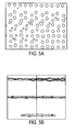
- FIGS. 5A-5B schematically depict exemplary semiconductor features Jetted in a non-Newtonian form in accordance with various embodiments of the present teachings.
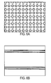
- FIGS. 6A-6B schematically depict exemplary semiconductor features jetted in a Newtonian form in accordance with various embodiments of the present teachings.
- FIGS. It should be noted that some details of the FIGS. have been simplified and are drawn to facilitate understanding of the embodiments rather than to maintain strict structural accuracy, detail, and scale.
- Exemplary embodiments provide materials and processes for forming organic semiconductor features.
- the formation of semiconductor features can include a rheological conversion of a liquid composition between a non-Newtonian "dispersion" having an un-defined viscosity and a Newtonian "solution” having a constant viscosity.
- uniform semiconductor features can be formed with improved deposition performance.
- FIG. 1 depicts an exemplary process for forming a semiconductor feature in accordance with various embodiments of the present teachings. While the process 100 of FIG. 1 is illustrated and described below as a series of acts or events, it will be appreciated that the present invention is not limited by the illustrated ordering of such acts or events. For example, some acts may occur in different orders and/or concurrently with other acts or events apart from those illustrated and/or described herein. Also, not all illustrated steps may be required to implement a methodology in accordance with one or more aspects or embodiments of the present invention. Further, one or more of the acts depicted herein may be carried out in one or more separate acts and/or phases.
- a liquid composition can be formed by dispersing one or more semiconductor materials in a suitable organic solvent.
- the semiconductor material can include one or more organic semiconductors having a formula (I) of the following: wherein A is a divalent linkage; R1 and R2 is independently selected from the group consisting of hydrogen, alkyl, arylalkyl, alkylaryl, perhaloalkyl, alkoxyalkyl, siloxy-substituted alkyl, polyether, alkoxy, and halogen; and n is from 2 to about 5,000.
- A is a divalent linkage
- R1 and R2 is independently selected from the group consisting of hydrogen, alkyl, arylalkyl, alkylaryl, perhaloalkyl, alkoxyalkyl, siloxy-substituted alkyl, polyether, alkoxy, and halogen
- n is from 2 to about 5,000.
- the divalent linkage A of formula (I) can include a structure selected from the following: and combinations thereof, wherein each R' is independently selected from the groups consisting of hydrogen, alkyl, substituted alkyl, aryl, substituted aryl, heteroaryl, halogen, -CN, and -NO 2 -.
- the semiconducting material can include a compound having the following formula: and wherein R1, R2, R', and R" are independently selected from i) hydrogen, ii) alkyl or substituted alkyl, iii) aryl or substituted aryl, iv) alkoxy or substituted alkoxy, v) a suitable hetero-containing group, vi) a halogen, or mixtures thereof; and n is an integer from about 2 to about 5,000, from about 2 to about 2,500, from about 2 to about 1,000, from about 100 to about 800, or from about 2 to about 100.
- the hydrocarbon can be alkyl, alkoxy, aryl, substituted derivatives thereof, and the like, inclusive of sidechains containing, for example, from zero to about 35 carbon atoms, or from about 1 to about 30 carbon atoms, or from about 1 to about 20 carbon atoms, or from about 6 to about 18 carbon atoms.
- R1 and R2 can be the same or different and each independently selected from a long carbon side-chain containing from about 6 to about 30 carbon atoms, or from about 6 to about 20 carbon atoms; and R' or R" can be the same or different and each independently selected from a substituent containing from 0 to about 5 carbon atoms; or R1 and R2 can be each independently selected from a substituent containing from 0 to about 5 carbon atoms, and R' can be a long carbon side-chain containing from 6 to about 30 carbon atoms.
- R 1 and R 2 , R', and R" can independently be alkyl with about 1 to about 35 carbon atoms of, for example, methyl, ethyl, propyl, butyl, pentyl, hexyl, heptyl, octyl, nonyl, decyl, undecyl, dodecyl, tridecyl, tetradecyl, pentadecyl, hexadecyl, heptadecyl or octadecyl; or arylalkyl with about 7 to about 42 carbon atoms of, for example, methylphenyl (tolyl), ethylphenyl, propylphenyl, butylphenyl, pentylphenyl, hexylphenyl, heptylphenyl, octylphenyl, nonylphenyl, decylphenyl,
- the semiconducting material can be a compound having the following formula: and
- the number average molecular weight (Mn) of the polymers in embodiments can be, for example, from about 500 to about 400,000, including from about 1,000 to about 150,000, and the weight average molecular weight (Mw) thereof can be from about 600 to about 500,000, including from about 1,500 to about 200,000, both as measured by, for example, gel permeation chromatography using polystyrene standards.
- the semiconducting material can be a compound of the formula (1). In another specific embodiment, the semiconducting material can be a compound of the formula (2) to (5).
- the type of solvent used can result in effective mixing or dispersion of the semiconductor materials in the solvent.
- the solvent can be an aromatic solvent.
- the solvent can be a halogenated aromatic solvent.
- Exemplary halogenated aromatic solvents can include chlorobenzene, dichlorobenzene (1,2-dichlorobenzene, and 1,3-dichlorobenzene), trichlorobenzene, or chlorotoluene.
- the solvent can include 1,2-dichlorobenzene.
- the solvent can be a non-halogenated solvent.
- Exemplary non-halogenated aromatic solvents can include toluene, xylene, mesitylene, trimethylbenezene, ethylbenzene, tetrahydronaphthalene, and the like.
- the solvent can be a non-aromatic solvent.
- Exemplary non-aromatic solvent can include chloroform, chloroethane, cyclohexane, bicyclohexyl and the like.
- the liquid composition can include poly(3,3"'-dialkylquaterthiophene) (PQT-12) dispersed in an exemplary solvent of dichlorobenzene.
- PQT-12 poly(3,3"'-dialkylquaterthiophene)
- the liquid composition can be formed to further include, for example, any suitable nanomaterials including, such as nanotubes, nanowires nanodots, quantum dots, nanorods, nanocrystals, nanotetrapods, nanotripods, nanobipods, nanoparticles, nanosaws, nanosprings, nanoribbons, and/or any other suitable nanomaterials or combination of nanomaterials to improve the carrier mobility and conductivity of the formed semiconductors.
- any suitable nanomaterials including, such as nanotubes, nanowires nanodots, quantum dots, nanorods, nanocrystals, nanotetrapods, nanotripods, nanobipods, nanoparticles, nanosaws, nanosprings, nanoribbons, and/or any other suitable nanomaterials or combination of nanomaterials to improve the carrier mobility and conductivity of the formed semiconductors.
- high temperatures that are above ambient temperature can be used to facilitate the dispersion/dissolution of organic semiconductors in the solvent. This can be followed by a cooling process to form the liquid composition at the ambient temperature.
- any suitable processes such as, for example, sonication or mechanical stirring, can be used to facilitate the dispersion/dissolution of organic semiconductors in the solvent.
- organic semiconductors can be dissolved in the solvent at an elevated temperature of, for example, up to about 80 °C depending on the organic semiconductors and the solvent used.
- the dispersion can then be formed by cooling the solution to room temperature (about 20-25 °C) to form the liquid composition, wherein the dissolved organic semiconductors aggregate, for example, into nano structures in the solvent.
- the dispersion can be ultra-sonicated, for example, during cooling.
- organic semiconductors can form semiconductor particles, such as, semiconductor aggregates or semiconductor nanoparticles in the solvent.
- the formed liquid composition containing semiconductor particles can be non-Newtonian having an un-defined viscosity. That is, the viscosity of the liquid composition containing semiconductor particles can change as a shear force applies to the liquid composition.
- the non-Newtonian liquid composition containing semiconductor particles can be stable at a first temperature ranging from 0 to about 50 °C, including the temperature from about 0°C to about 40 °C or from about 20 °C to about 40 °C.
- the non-Newtonian liquid composition containing semiconductor particles can have a long shelf-life, for example, at least about two days.
- Other embodiments can include a stable non-Newtonian liquid composition having a long shelf-life of, for example, up to about 1 year or longer. The stability of the non-Newtonian liquid composition at the first temperature can allow for easy storage and transfer prior to further processing.
- semiconductor particles in the non-Newtonian liquid composition can include various shapes, regular or irregular, and various dimensions.
- the semiconductor particles can include aggregates in a nanometer scale having at least one minor dimension of about 1000 nm or less.
- the semiconductor nanoparticles in the non-Newtonian liquid composition can be in various forms, regular or irregular, including, but not limited to, nanotubes, nanofibrils, nanorods, nanobelt, nanoshafts, nanopillars, nanowires, nanoneedles or their combinations.
- from about 0.5% to about 100% of the semiconductor in the non-Newtonian liquid composition can be nano aggregates. In some embodiments, at least about 30% of the semiconductor in the non-Newtonian liquid composition can be nano aggregates. In other embodiments, from about 50 % to about 80% of semiconductor in the non-Newtonian liquid composition can be nano aggregates.
- non-Newtonian liquid composition containing the semiconductor particles is directly deposited onto a substrate, for example, jetted onto the substrate, undesired defects may be observed because the shear viscosity of the non-Newtonian liquid composition may change in the print-head when being jetted at high frequency.
- the non-Newtonian liquid composition formed at step 110 can be temporarily converted into a Newtonian liquid composition. That is, stress versus rate of strain curve of the liquid composition can be linear and pass through the origin.
- the Newtonian liquid composition can thus have a constant viscosity determined by constant of that proportionality.
- the non-Newtonian liquid composition can be converted into a Newtonian liquid composition by a heating process, or other suitable processes, in embodiments.
- the heating process can be conducted, for example, using elevated temperatures or in a step-wise manner.
- the heating temperature can be selected depending on a conversion temperature between a non-Newtonian state and a Newtonian state of certain liquid compositions.
- the conversion temperature can in turn be determined by, e.g., measuring the rheological properties of the liquid composition. For example, an oscillatory measurement can be used to measure the complex viscosity of a non-Newtonian liquid composition as function of the temperature.
- the conversion temperature can be a starting temperature or a temperature range when the complex viscosity of the liquid composition becomes constant, which means the liquid composition becomes a uniform Newtonian solution.
- semiconductor particles can be uniformly or completely dissolved in the solvent and, in some cases, no aggregates or particles can be observed in the uniform Newtonian solution.
- the Newtonian solution can be substantially absent of aggregates or particle of the organic semiconductor.
- the non-Newtonian liquid composition can be heated to a second temperature.
- the second temperature can be the conversion temperature (or the conversion temperature range) or be greater than the conversion temperature (or the conversion temperature range) of a specific liquid composition.
- the non-Newtonian liquid composition can be heated at elevated temperatures from about 20 °C to about 120 °C or in some cases from about 40 °C to about 120 °C.
- the non-Newtonian liquid composition containing semiconductor particles can be heated for a conversion at elevated temperatures ranging from about 45°C to about 80 °C.
- the non-Newtonian liquid composition containing semiconductor particles can then be converted into a uniform solution of Newtonian liquid composition.
- such conversion can be performed in a time period of, for example, less than about 1 hour.
- the conversion from a non-Newtonian form to a Newtonian form can take about 30 minutes less and in some embodiments about 10 minutes or less.
- quick conversion can be achieved of about 1 minute or less.
- the Newtonian liquid composition can be equilibrated for a period of time, such as about 1 hour or less. In some embodiments, the Newtonian liquid composition can be equilibrated for about 30 minutes less or in some embodiments about 10 minutes or less. In other embodiments, the Newtonian liquid composition can be equilibrated for about 1 minute or less. In embodiments, the liquid composition can be kept at the second temperature for a short time so as to avoid the degradation of organic semiconductors.
- the heating can be performed by using a heater, for example, an oven, a radiant energy source, a thermocouple, or a combination thereof.
- the Newtonian liquid composition can be deposited into semiconductor features on a substrate.
- the deposited semiconductor features can then be solidified or dried, for example, by an evaporation or a heating process.
- Various semiconductor features, such as semiconductor layers, patterns, lines or dots, can then be formed.
- the deposition can be performed using a printing or a coating technique.
- exemplary printing techniques can include inkjet printing, lithographic or offset printing, flexographic printing, screen printing, stencil printing, stamping, micro-contact printing, gravure, and the like.
- Exemplary coating techniques can include spin coating, blade coating, rod coating, dip coating, and the like.
- the deposition can be inkjet printing.
- a predetermined array can be designed in order to form an array of semiconductor features including for example, the semiconductor layers, patterns, lines or dots as described above.
- each semiconductor feature in the resulting array may have an offset, i.e., a center-to-center spacing, from its original design.
- the offset can range from 0 to about 30 microns, or in some embodiments, from 0 to about 20 microns. In other embodiments, the offset between a formed semiconductor feature and its original design can be less than about 10 microns.
- FIG. 2 depicts an exemplary system 200 for printing semiconductor features in accordance with various embodiments of present teachings. It should be readily apparent to one of ordinary skill in the art that the system 200 depicted in FIG. 2 represents a generalized schematic illustration and that other components/ devices can be added or existing components/ devices can be removed or modified.
- the system 200 can include a printable substrate 205, and a printing station including a cartridge 210, one or more print-heads 220 each having a jet nozzle 225, and a heater 230.
- the cartridge 210 can be used for supplying ink dispersion, in embodiments, such as the non-Newtonian liquid composition containing semiconductor particles.
- the heater 230 can be configured with the print-heads 220 and/or the jet nozzle 225 so as to heat the non-Newtonian liquid composition that passes the print-heads 220 and/or the jet nozzle 225. In this manner, the non-Newtonian liquid composition dispersion containing semiconductor particles can be converted in-situ into a Newtonian liquid composition solution.
- the occurrence of clogging of the ink-jet nozzles can be minimized, and the uniformity of the printing or the jetting as well as the uniformity of deposited semiconductor features can be achieved.
- the heated non-Newtonian liquid composition can then be jetted through the jet nozzle 225 onto a printable substrate 205.
- the printable substrate 205 can be configured to receive the jetted liquid composition to form semiconductor features through, for example, a drying process.
- the surface of the printable substrate prior to the deposition of the Newtonian liquid composition, can be chemically treated or mechanically rubbed.
- the printable substrate can be an organic substrate, an inorganic substrate, a flexible substrate or a rigid substrate.
- the printable substrate can include, for example, glass, silicon (including electrode bearing silicon substrates), polyimide, polyethylene terephthalate (PET), poly(ethylenenaphthalate) (PEN), indium tin oxide (ITO), or any other suitable substrate.
- the substrate can be at a third temperature.
- the third temperature can be, for example, from about 0 to about 120 °C, including from about 20 °C to about 80 °C, or from about 20 °C to about 40 °C.
- the third temperature can be similar to the first temperature, for example, to be lower than the conversion temperature of the liquid composition.
- the Newtonian fluid can become non-Newtonian fluid when it reaches the substrate. That is, nano-aggregates or gel can be re-formed at the substrate.
- the liquid composition can undergo a phase change from non-Newtonian state (having nano aggregates phase, or the dispersion phase) to a Newtonian state (substantially absent of nano aggregates in the solution phase), and back to non-Newtonian state (having nano aggregates phase, or the dispersion phase).
- This phase change printing process can enable high accuracy jetting at Newtonian state, and low spreading or well confined drops of the liquid composition upon the substrate due to the reversion to the non-Newtonian state.
- the feature of non-Newtonian ink fluid having high viscosity at low shear rate can facilitate to confine the ink drops and to reduce spreading.
- the process 100 and/or system 200 disclosed herein can be used for forming devices such as, for example, transistors, sensors, light emitting diodes, photovoltaic devices, or any other suitable device or combination of devices.
- Organic semiconductor PQT was used as an exemplary organic semiconductor for forming semiconductor features.
- the organic semiconductor PQT had the following structure:
- the non-Newtonian liquid composition containing PQT semiconductor particles was prepared by dissolving PQT-12 semiconductor in a solvent of 1,2-dichlorobenzene at an elevated temperature of up to about 80 °C, followed by a cooling process. During cooling, the particle dispersion was sonicated. Purple color dispersion containing PQT and/or nano-PQT particles was obtained, which was very stable at room temperature, for example, having a shelf-life over about 1 year.
- Rheological properties of the PQT-dispersion were measured using RFS3 Fluids Spectrometer (TA Instruments, New Castle, Delaware) with a cone and plate geometry. Ti (titanium) based cone was used with a nominal cone angle of 0.02 radians and a gap of 48.3 microns.
- FIG. 3 shows measured results, which indicate that the PQT-dispersion is a non-Newtonian fluid.
- the PQT-dispersion has a shear thinning property (or a pseudoplastic property), i.e., having high viscosity (e.g., over 100 cps) at low shearing rates and having low viscosity (e.g., about 2-3 cps) at high shearing rates (e.g., about 10 3 s -1 ).
- the exemplary PQT-dispersion had a conversion temperature or a narrow conversion temperature range at around 40 °C for changing from a non-Newtonian dispersion into a Newtonian solution.
- Dimatix inkjet printer equipped with 10 pL cartridges was used in this comparative (or control) example.
- the print-head was set at room temperature.
- PQT-dispersion of Example 2 was deposited at a non-Newtonian form.
- a 4X4 cm dot-array spaced by 100 ⁇ m, and two straight lines each having single-drop width were designed and printed as examples.
- FIGS. 5A-5B depict exemplary semiconductor features Jetted at a non-Newtonian form in accordance with various embodiments of the present teachings.
- FIG. 5A schematically depicts the jetted results of dot-array. As shown, mis-directional deposition was observed although most of the area showed a regular dots array similar to the designed pattern.
- FIG. 5B schematically depicts the jetted results of thin lines. Rough edges and/or broken area were also observed for this non-Newtonian PQT-dispersion of Example 2.
- Example 4 same printer and cartridges were used as for Example 4.
- the print-head of the cartridges was set at 60 °C, which is higher than the convention temperature as indicated by Example 3. Therefore, when the PQT-dispersion of Example 2 passed through the print-head, the particle dispersion can be changed into Newtonian solution that was then jetted out of the nozzles. Same pattern designs shown in FIGS. 5A-5B were printed for comparison purpose.
- FIGS. 6A-6B depict exemplary semiconductor features jetted at a Newtonian form in accordance with various embodiments of the present teachings.
- FIG. 6A schematically depicts the jetted results of dot-array. As shown, no misfired drop was observed for the whole 4X4 cm array.
- FIG. 6B schematically depicts the jetted results of thin lines. As shown, the printed lines were observed to be smooth and uniform, without any broken area.
- FIGS. 6A-6B indicates high quality semiconductor prints or semiconductor features achieved by using the disclosed processes and systems.
Landscapes
- Engineering & Computer Science (AREA)
- Manufacturing & Machinery (AREA)
- Thin Film Transistor (AREA)
- Liquid Deposition Of Substances Of Which Semiconductor Devices Are Composed (AREA)
- Electroluminescent Light Sources (AREA)
- Polyoxymethylene Polymers And Polymers With Carbon-To-Carbon Bonds (AREA)
Abstract
Description
- The present invention relates to organic semiconductors and, more particularly, to materials and methods for organic semiconductors having enhanced printing performance.
- Semiconductor technology has played an important role in the development of electronic circuits over the past several decades. Two examples of semiconductor technology include complementary metal oxide semiconductor (CMOS) processing technology and organic semiconductor processing technology.
- Organic semiconductor processing technology was developed more recently, wherein organic materials that exhibit semiconducting properties are used to fabricate electronic and optoelectronic devices on substrates that are rigid or flexible.
- Compared to CMOS processing technology, organic semiconductor processing technology is cheaper to implement and more suitable to specific applications such as flexible electronics and displays. This is particularly advantageous for large area displays and low-cost RFID tags.
- Conventional methods for forming organic semiconductors include printing a particle-containing dispersion onto a substrate. The printable dispersion is often a non-Newtonian fluid, in which the viscosity changes with applied strain rate. Such dispersion having a viscosity that is not well defined may cause poor jetted performance during printing. For example, significant offsets from original design are often observed for the printed organic semiconductor features, including nonuniform or broken line or patterns, rough edges, etc.
- Thus, there is a need to overcome these and other problems of the prior art and to improve deposition performance of organic semiconductor features.
- According to various embodiments, the present invention includes a process for forming a semiconductor feature by first providing a liquid composition that includes one or more organic semiconductors. The liquid composition can then be converted from a non-Newtonian form at a first temperature to a Newtonian form at a second temperature. The converted liquid composition in the Newtonian form can then be deposited on a substrate to form one or more semiconductor features.
- According to various embodiments, the present teachings also include a process for forming a semiconductor feature. In this method, a liquid composition that includes a plurality of organic semiconductor particles dispersed in a solvent can be formed to have a shelf-life of more than about two days. The liquid composition can then be heated so as to uniformly dissolve the plurality of organic semiconductor particles in the solvent to form a Newtonian liquid composition, which can then be printed onto a substrate to form one or more uniform semiconductor features.
- Additional objects and advantages of the present teachings will be set forth in part in the description which follows, and in part will be obvious from the description, or may be learned by practice of the present teachings. The objects and advantages of the present teachings will be realized and attained by means of the elements and combinations particularly pointed out in the appended claims.
- It is to be understood that both the foregoing general description and the following detailed description are exemplary and explanatory only and are not restrictive of the present teachings, as claimed.
- The accompanying drawings, which are incorporated in and constitute a part of this specification, illustrate several embodiments of the present teachings and together with the description, serve to explain the principles of the present teachings.
-
FIG. 1 depicts an exemplary method for forming an organic semiconductor feature in accordance with various embodiments of the present teachings. -
FIG. 2 depicts an exemplary printing system for forming an organic semiconductor feature in accordance with various embodiments of the present teachings. -
FIG. 3 depicts an exemplary rheological test result for an exemplary non-Newtonian liquid composition in accordance with various embodiments of the present teachings. -
FIG. 4 depicts a conversion from non-Newtonian to Newtonian of an exemplary liquid composition in accordance with various embodiments of the present teachings. -
FIGS. 5A-5B schematically depict exemplary semiconductor features Jetted in a non-Newtonian form in accordance with various embodiments of the present teachings. -
FIGS. 6A-6B schematically depict exemplary semiconductor features jetted in a Newtonian form in accordance with various embodiments of the present teachings. - It should be noted that some details of the FIGS. have been simplified and are drawn to facilitate understanding of the embodiments rather than to maintain strict structural accuracy, detail, and scale.
- Reference will now be made in detail to embodiments of the present teachings, examples of which are illustrated in the accompanying drawings.
- In the following description, reference is made to the accompanying drawings that form a part thereof, and in which is shown by way of illustration specific exemplary embodiments in which the present teachings may be practiced. Exemplary embodiments provide materials and processes for forming organic semiconductor features. In one embodiment, the formation of semiconductor features can include a rheological conversion of a liquid composition between a non-Newtonian "dispersion" having an un-defined viscosity and a Newtonian "solution" having a constant viscosity. In embodiments, uniform semiconductor features can be formed with improved deposition performance.
-
FIG. 1 depicts an exemplary process for forming a semiconductor feature in accordance with various embodiments of the present teachings. While theprocess 100 ofFIG. 1 is illustrated and described below as a series of acts or events, it will be appreciated that the present invention is not limited by the illustrated ordering of such acts or events. For example, some acts may occur in different orders and/or concurrently with other acts or events apart from those illustrated and/or described herein. Also, not all illustrated steps may be required to implement a methodology in accordance with one or more aspects or embodiments of the present invention. Further, one or more of the acts depicted herein may be carried out in one or more separate acts and/or phases. - At 110 of
FIG. 1 , a liquid composition can be formed by dispersing one or more semiconductor materials in a suitable organic solvent. - In embodiments, the semiconductor material can include one or more organic semiconductors having a formula (I) of the following:

- In embodiments, the divalent linkage A of formula (I) can include a structure selected from the following:


- In further embodiments, the semiconducting material can include a compound having the following formula:


- In embodiments, R1 and R2 can be the same or different and each independently selected from a long carbon side-chain containing from about 6 to about 30 carbon atoms, or from about 6 to about 20 carbon atoms; and R' or R" can be the same or different and each independently selected from a substituent containing from 0 to about 5 carbon atoms; or R1 and R2 can be each independently selected from a substituent containing from 0 to about 5 carbon atoms, and R' can be a long carbon side-chain containing from 6 to about 30 carbon atoms.
- In embodiments, R1 and R2, R', and R" can independently be alkyl with about 1 to about 35 carbon atoms of, for example, methyl, ethyl, propyl, butyl, pentyl, hexyl, heptyl, octyl, nonyl, decyl, undecyl, dodecyl, tridecyl, tetradecyl, pentadecyl, hexadecyl, heptadecyl or octadecyl; or arylalkyl with about 7 to about 42 carbon atoms of, for example, methylphenyl (tolyl), ethylphenyl, propylphenyl, butylphenyl, pentylphenyl, hexylphenyl, heptylphenyl, octylphenyl, nonylphenyl, decylphenyl, undecylphenyl, dodecylphenyl, tridecylphenyl, tetradecylphenyl, pentadecylphenyl, hexadecylphenyl, heptadecylphenyl, and octadecylphenyl. In other embodiments, R1, R2, R' and R" can independently represent alkyl or substituted alkyl groups having from about 1 to about 35 carbon atoms.
- In a specific embodiment, the semiconducting material can be a compound having the following formula:


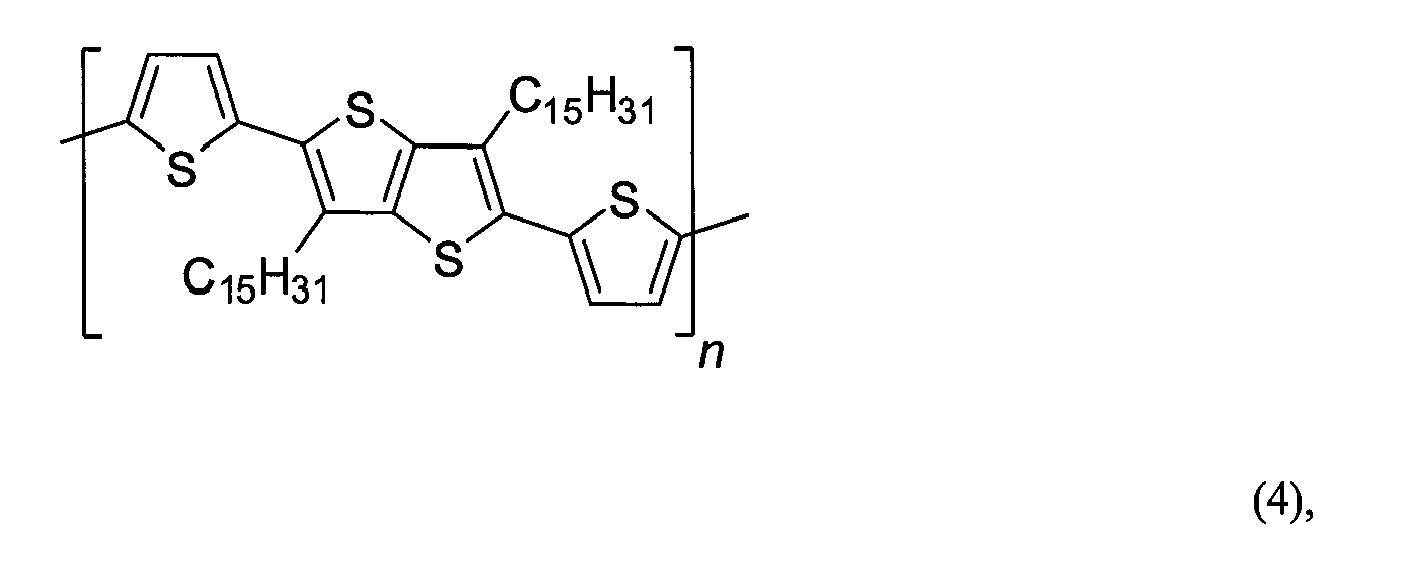


- In a specific embodiment, the semiconducting material can be a compound of the formula (1). In another specific embodiment, the semiconducting material can be a compound of the formula (2) to (5).
- In embodiments, the type of solvent used can result in effective mixing or dispersion of the semiconductor materials in the solvent. In embodiments, the solvent can be an aromatic solvent. In some embodiments, the solvent can be a halogenated aromatic solvent. Exemplary halogenated aromatic solvents can include chlorobenzene, dichlorobenzene (1,2-dichlorobenzene, and 1,3-dichlorobenzene), trichlorobenzene, or chlorotoluene. In a specific embodiment, the solvent can include 1,2-dichlorobenzene. In some embodiments, the solvent can be a non-halogenated solvent. Exemplary non-halogenated aromatic solvents can include toluene, xylene, mesitylene, trimethylbenezene, ethylbenzene, tetrahydronaphthalene, and the like. In some embodiments, the solvent can be a non-aromatic solvent. Exemplary non-aromatic solvent can include chloroform, chloroethane, cyclohexane, bicyclohexyl and the like.
- In an exemplary embodiment, the liquid composition can include poly(3,3"'-dialkylquaterthiophene) (PQT-12) dispersed in an exemplary solvent of dichlorobenzene.
- In embodiments, in addition to organic semiconductors, the liquid composition can be formed to further include, for example, any suitable nanomaterials including, such as nanotubes, nanowires nanodots, quantum dots, nanorods, nanocrystals, nanotetrapods, nanotripods, nanobipods, nanoparticles, nanosaws, nanosprings, nanoribbons, and/or any other suitable nanomaterials or combination of nanomaterials to improve the carrier mobility and conductivity of the formed semiconductors.
- In embodiments, high temperatures that are above ambient temperature (e.g., about 20-25°C) can be used to facilitate the dispersion/dissolution of organic semiconductors in the solvent. This can be followed by a cooling process to form the liquid composition at the ambient temperature. In embodiments, any suitable processes, such as, for example, sonication or mechanical stirring, can be used to facilitate the dispersion/dissolution of organic semiconductors in the solvent.
- For example, organic semiconductors can be dissolved in the solvent at an elevated temperature of, for example, up to about 80 °C depending on the organic semiconductors and the solvent used. The dispersion can then be formed by cooling the solution to room temperature (about 20-25 °C) to form the liquid composition, wherein the dissolved organic semiconductors aggregate, for example, into nano structures in the solvent. In embodiments, the dispersion can be ultra-sonicated, for example, during cooling.
- In embodiments, organic semiconductors can form semiconductor particles, such as, semiconductor aggregates or semiconductor nanoparticles in the solvent. As a result, the formed liquid composition containing semiconductor particles can be non-Newtonian having an un-defined viscosity. That is, the viscosity of the liquid composition containing semiconductor particles can change as a shear force applies to the liquid composition.
- In various embodiments, the non-Newtonian liquid composition containing semiconductor particles can be stable at a first temperature ranging from 0 to about 50 °C, including the temperature from about 0°C to about 40 °C or from about 20 °C to about 40 °C. In addition, the non-Newtonian liquid composition containing semiconductor particles can have a long shelf-life, for example, at least about two days. Other embodiments can include a stable non-Newtonian liquid composition having a long shelf-life of, for example, up to about 1 year or longer. The stability of the non-Newtonian liquid composition at the first temperature can allow for easy storage and transfer prior to further processing.
- In various embodiments, semiconductor particles in the non-Newtonian liquid composition can include various shapes, regular or irregular, and various dimensions. For example, the semiconductor particles can include aggregates in a nanometer scale having at least one minor dimension of about 1000 nm or less. In embodiments, the semiconductor nanoparticles in the non-Newtonian liquid composition can be in various forms, regular or irregular, including, but not limited to, nanotubes, nanofibrils, nanorods, nanobelt, nanoshafts, nanopillars, nanowires, nanoneedles or their combinations.
- In various embodiments, from about 0.5% to about 100% of the semiconductor in the non-Newtonian liquid composition can be nano aggregates. In some embodiments, at least about 30% of the semiconductor in the non-Newtonian liquid composition can be nano aggregates. In other embodiments, from about 50 % to about 80% of semiconductor in the non-Newtonian liquid composition can be nano aggregates.
- In various embodiments, if non-Newtonian liquid composition containing the semiconductor particles is directly deposited onto a substrate, for example, jetted onto the substrate, undesired defects may be observed because the shear viscosity of the non-Newtonian liquid composition may change in the print-head when being jetted at high frequency.
- At 120, the non-Newtonian liquid composition formed at
step 110 can be temporarily converted into a Newtonian liquid composition. That is, stress versus rate of strain curve of the liquid composition can be linear and pass through the origin. The Newtonian liquid composition can thus have a constant viscosity determined by constant of that proportionality. - Various techniques can be used to conduct such rheological conversion of the liquid composition. For example, the non-Newtonian liquid composition can be converted into a Newtonian liquid composition by a heating process, or other suitable processes, in embodiments. The heating process can be conducted, for example, using elevated temperatures or in a step-wise manner. In embodiments, the heating temperature can be selected depending on a conversion temperature between a non-Newtonian state and a Newtonian state of certain liquid compositions.
- In various embodiments, the conversion temperature can in turn be determined by, e.g., measuring the rheological properties of the liquid composition. For example, an oscillatory measurement can be used to measure the complex viscosity of a non-Newtonian liquid composition as function of the temperature. The conversion temperature can be a starting temperature or a temperature range when the complex viscosity of the liquid composition becomes constant, which means the liquid composition becomes a uniform Newtonian solution. During this conversion, semiconductor particles can be uniformly or completely dissolved in the solvent and, in some cases, no aggregates or particles can be observed in the uniform Newtonian solution. In certain embodiment, the Newtonian solution can be substantially absent of aggregates or particle of the organic semiconductor.
- In various embodiments, the non-Newtonian liquid composition can be heated to a second temperature. The second temperature can be the conversion temperature (or the conversion temperature range) or be greater than the conversion temperature (or the conversion temperature range) of a specific liquid composition. In exemplary embodiments, the non-Newtonian liquid composition can be heated at elevated temperatures from about 20 °C to about 120 °C or in some cases from about 40 °C to about 120 °C. In other exemplary embodiments, the non-Newtonian liquid composition containing semiconductor particles can be heated for a conversion at elevated temperatures ranging from about 45°C to about 80 °C.
- The non-Newtonian liquid composition containing semiconductor particles can then be converted into a uniform solution of Newtonian liquid composition.
- In embodiments, such conversion can be performed in a time period of, for example, less than about 1 hour. In some embodiments, the conversion from a non-Newtonian form to a Newtonian form can take about 30 minutes less and in some embodiments about 10 minutes or less. In further embodiments, quick conversion can be achieved of about 1 minute or less.
- In embodiments, after the conversion, the Newtonian liquid composition can be equilibrated for a period of time, such as about 1 hour or less. In some embodiments, the Newtonian liquid composition can be equilibrated for about 30 minutes less or in some embodiments about 10 minutes or less. In other embodiments, the Newtonian liquid composition can be equilibrated for about 1 minute or less. In embodiments, the liquid composition can be kept at the second temperature for a short time so as to avoid the degradation of organic semiconductors.
- In various embodiments, other conversion temperatures, conversion temperature ranges, and/or equilibration times can be used, depending on materials and methods used for the liquid composition.
- In various embodiments, the heating can be performed by using a heater, for example, an oven, a radiant energy source, a thermocouple, or a combination thereof.
- At 130 of
FIG. 1 , the Newtonian liquid composition can be deposited into semiconductor features on a substrate. The deposited semiconductor features can then be solidified or dried, for example, by an evaporation or a heating process. Various semiconductor features, such as semiconductor layers, patterns, lines or dots, can then be formed. - In various embodiments, the deposition can be performed using a printing or a coating technique. Exemplary printing techniques can include inkjet printing, lithographic or offset printing, flexographic printing, screen printing, stencil printing, stamping, micro-contact printing, gravure, and the like. Exemplary coating techniques can include spin coating, blade coating, rod coating, dip coating, and the like. In one embodiment, the deposition can be inkjet printing.
- In embodiments, during deposition of the Newtonian liquid composition, a predetermined array can be designed in order to form an array of semiconductor features including for example, the semiconductor layers, patterns, lines or dots as described above.
- In embodiments, each semiconductor feature in the resulting array may have an offset, i.e., a center-to-center spacing, from its original design. In embodiments, the offset can range from 0 to about 30 microns, or in some embodiments, from 0 to about 20 microns. In other embodiments, the offset between a formed semiconductor feature and its original design can be less than about 10 microns.
-
FIG. 2 depicts anexemplary system 200 for printing semiconductor features in accordance with various embodiments of present teachings. It should be readily apparent to one of ordinary skill in the art that thesystem 200 depicted inFIG. 2 represents a generalized schematic illustration and that other components/ devices can be added or existing components/ devices can be removed or modified. - As shown in
FIG. 2 , thesystem 200 can include aprintable substrate 205, and a printing station including acartridge 210, one or more print-heads 220 each having ajet nozzle 225, and aheater 230. - The
cartridge 210 can be used for supplying ink dispersion, in embodiments, such as the non-Newtonian liquid composition containing semiconductor particles. - The
heater 230 can be configured with the print-heads 220 and/or thejet nozzle 225 so as to heat the non-Newtonian liquid composition that passes the print-heads 220 and/or thejet nozzle 225. In this manner, the non-Newtonian liquid composition dispersion containing semiconductor particles can be converted in-situ into a Newtonian liquid composition solution. - In embodiments, due to the Newtonian feature of the liquid composition, the occurrence of clogging of the ink-jet nozzles can be minimized, and the uniformity of the printing or the jetting as well as the uniformity of deposited semiconductor features can be achieved.
- The heated non-Newtonian liquid composition can then be jetted through the
jet nozzle 225 onto aprintable substrate 205. Theprintable substrate 205 can be configured to receive the jetted liquid composition to form semiconductor features through, for example, a drying process. - In one embodiment, prior to the deposition of the Newtonian liquid composition, the surface of the printable substrate can be chemically treated or mechanically rubbed. In embodiments, the printable substrate can be an organic substrate, an inorganic substrate, a flexible substrate or a rigid substrate. In embodiments, the printable substrate can include, for example, glass, silicon (including electrode bearing silicon substrates), polyimide, polyethylene terephthalate (PET), poly(ethylenenaphthalate) (PEN), indium tin oxide (ITO), or any other suitable substrate.
- In embodiments, the substrate can be at a third temperature. The third temperature can be, for example, from about 0 to about 120 °C, including from about 20 °C to about 80 °C, or from about 20 °C to about 40 °C. In further embodiments, the third temperature can be similar to the first temperature, for example, to be lower than the conversion temperature of the liquid composition. In other words, the Newtonian fluid can become non-Newtonian fluid when it reaches the substrate. That is, nano-aggregates or gel can be re-formed at the substrate. In view the whole process, the liquid composition can undergo a phase change from non-Newtonian state (having nano aggregates phase, or the dispersion phase) to a Newtonian state (substantially absent of nano aggregates in the solution phase), and back to non-Newtonian state (having nano aggregates phase, or the dispersion phase). This phase change printing process can enable high accuracy jetting at Newtonian state, and low spreading or well confined drops of the liquid composition upon the substrate due to the reversion to the non-Newtonian state. The feature of non-Newtonian ink fluid having high viscosity at low shear rate can facilitate to confine the ink drops and to reduce spreading.
- In embodiments, the
process 100 and/orsystem 200 disclosed herein can be used for forming devices such as, for example, transistors, sensors, light emitting diodes, photovoltaic devices, or any other suitable device or combination of devices. - The following examples are illustrative of the invention and its advantageous properties, and are not to be taken as limiting the disclosure or claims in any way.
- Examples
- Example 1- Organic Semiconductor PQT
- Organic semiconductor PQT was used as an exemplary organic semiconductor for forming semiconductor features. The organic semiconductor PQT had the following structure:

- Example 2- PQT-Dispersion or Non-Newtonian Liquid Composition Containing PQT Semiconductor Particles
- The non-Newtonian liquid composition containing PQT semiconductor particles was prepared by dissolving PQT-12 semiconductor in a solvent of 1,2-dichlorobenzene at an elevated temperature of up to about 80 °C, followed by a cooling process. During cooling, the particle dispersion was sonicated. Purple color dispersion containing PQT and/or nano-PQT particles was obtained, which was very stable at room temperature, for example, having a shelf-life over about 1 year.
- Rheological properties of the PQT-dispersion were measured using RFS3 Fluids Spectrometer (TA Instruments, New Castle, Delaware) with a cone and plate geometry. Ti (titanium) based cone was used with a nominal cone angle of 0.02 radians and a gap of 48.3 microns.
- A steady rate sweep test was performed for the PQT-dispersion at about 25°C and at a frequency ranging from 1 to 1000 s-1.
FIG. 3 shows measured results, which indicate that the PQT-dispersion is a non-Newtonian fluid. Specifically,FIG. 3 shows the PQT-dispersion has a shear thinning property (or a pseudoplastic property), i.e., having high viscosity (e.g., over 100 cps) at low shearing rates and having low viscosity (e.g., about 2-3 cps) at high shearing rates (e.g., about 103 s-1). - Example 3- Conversion from a Non-Newtonian Form to a Newtonian Form
- Small amplitude oscillatory measurement was conducted for the PQT-dispersion of Example 2, wherein the Non-Newtonian dispersion was heated at an elevated temperature from about 25°C to about 65°C with a temperature increment of about 2°C. Each increased temperature had an equilibration time of about 120 seconds.
- During this rheological oscillatory measurement, a constant frequency of about 1 Hz was used. As shown in
FIG. 4 , when the PQT-dispersion was gradually heated from room temperature to about 40 °C, the complex viscosity is gradually decreased. The complex viscosity however becomes constant once the temperature was increased at about 40 °C or greater, e.g., up to about 65 °C in this example, showing a Newtonian characteristic. In other words, the exemplary PQT-dispersion had a conversion temperature or a narrow conversion temperature range at around 40 °C for changing from a non-Newtonian dispersion into a Newtonian solution. - Example 4 - Semiconductor Features Jetted at Non-Newtonian Form
- Dimatix inkjet printer equipped with 10 pL cartridges was used in this comparative (or control) example. The print-head was set at room temperature. PQT-dispersion of Example 2 was deposited at a non-Newtonian form. A 4X4 cm dot-array spaced by 100 □m, and two straight lines each having single-drop width were designed and printed as examples.
-
FIGS. 5A-5B depict exemplary semiconductor features Jetted at a non-Newtonian form in accordance with various embodiments of the present teachings. - Specifically,
FIG. 5A schematically depicts the jetted results of dot-array. As shown, mis-directional deposition was observed although most of the area showed a regular dots array similar to the designed pattern.FIG. 5B schematically depicts the jetted results of thin lines. Rough edges and/or broken area were also observed for this non-Newtonian PQT-dispersion of Example 2. - Example 5 -Semiconductor Features Jetted at Newtonian Form
- In this example, same printer and cartridges were used as for Example 4. The print-head of the cartridges was set at 60 °C, which is higher than the convention temperature as indicated by Example 3. Therefore, when the PQT-dispersion of Example 2 passed through the print-head, the particle dispersion can be changed into Newtonian solution that was then jetted out of the nozzles. Same pattern designs shown in
FIGS. 5A-5B were printed for comparison purpose. -
FIGS. 6A-6B depict exemplary semiconductor features jetted at a Newtonian form in accordance with various embodiments of the present teachings. - Specifically,
FIG. 6A schematically depicts the jetted results of dot-array. As shown, no misfired drop was observed for the whole 4X4 cm array.FIG. 6B schematically depicts the jetted results of thin lines. As shown, the printed lines were observed to be smooth and uniform, without any broken area. - As compared with
FIGS. 5A-5B ,FIGS. 6A-6B indicates high quality semiconductor prints or semiconductor features achieved by using the disclosed processes and systems.
Claims (15)
- A process for forming a semiconductor feature comprising:providing a liquid composition comprising one or more organic semiconductors;converting the liquid composition from a non-Newtonian form at a first temperature to a Newtonian form at a second temperature; anddepositing the converted liquid composition on a substrate to form one or more semiconductor features.
- The process of claim 1, further comprising:determining a conversion temperature for the converting step, andheating the liquid composition from the first temperature to the second temperature,
wherein the second temperature is the determined conversion temperature or a temperature greater than the determined conversion temperature. - The process of claim 1, wherein the second temperature is an elevated temperature ranging from about 40 °C to about 120 °C.
- The process of claim 1, wherein the liquid composition is uniformly deposited by printing or coating, or
wherein the depositing is inkjet printing, or
wherein the converting step takes less than about 30 minutes. - The process of claim 1, further comprising an equilibrium time at the second temperature after conversion, wherein the equilibrium time is of less than about 30 minutes.
- The process of claim 1, wherein the first temperature ranges from about 0 to about 50 °C. or
wherein at least about 30% of the one or more organic semiconductors in the liquid composition are nano-aggregates at the first temperature. - The process of claim 1, wherein the liquid composition in the Newtonian form is substantially absent of aggregates of the one or more organic semiconductors.
- The process of claim 1, wherein the one or more organic semiconductors have a formula of:

wherein the divalent linkage A is selected from the group consisting of


- The process of claim 1, further comprising depositing the liquid composition according to an array design to form the one or more semiconductor features, wherein each semiconductor feature has an offset from an original design of the array design, the offset ranging from 0 to about 30 microns, or
wherein the substrate is at a third temperature ranging from about 0 to about 120 °C. - A process for forming a semiconductor feature comprising:forming a non-Newtonian liquid composition comprising a plurality of organic semiconductor particles dispersed in a solvent; wherein the non-Newtonian liquid composition has a shelf-life of more than about two days;heating the liquid composition to uniformly dissolve the plurality of organic semiconductor particles in the solvent to form a Newtonian liquid composition; anddepositing the Newtonian liquid composition onto a substrate to form one or more uniform semiconductor features on the substrate.
- The process of claim 15, wherein the heating step is performed by a heater configured with a print-head for heating the liquid composition that passes the print-head to have a constant viscosity.
- The process of claim 15, wherein the liquid composition is heated at a temperature elevated from about 40 °C to about 120 °C.
- The process of claim 15, wherein at least about 30% of the plurality of semiconductor particles are nano-aggregates.
- The process of claim 15, wherein the plurality of organic semiconductor particles have a formula of:


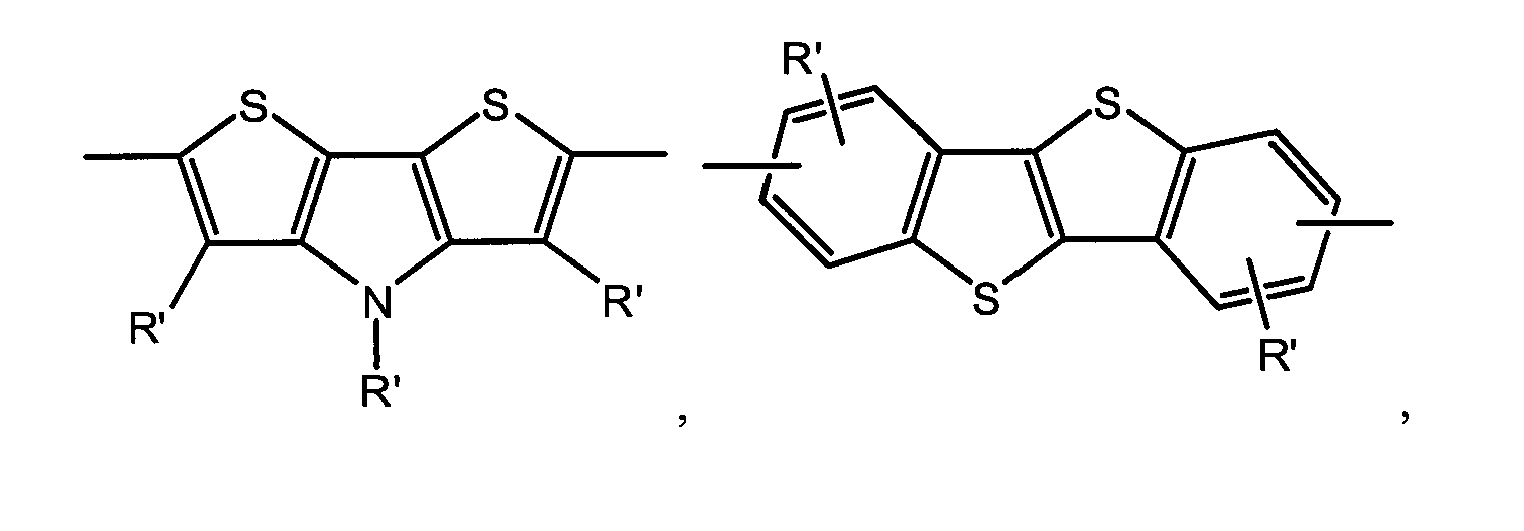

- The process of claim 15, wherein the one or more semiconductor features are features formed for a transistor, sensor, light emitting diode, or photovoltaic device.
Applications Claiming Priority (1)
| Application Number | Priority Date | Filing Date | Title |
|---|---|---|---|
| US12/560,032 US8030126B2 (en) | 2009-09-15 | 2009-09-15 | Printing process for enhanced jetted performance of semiconductor layer |
Publications (3)
| Publication Number | Publication Date |
|---|---|
| EP2296202A2 true EP2296202A2 (en) | 2011-03-16 |
| EP2296202A3 EP2296202A3 (en) | 2014-05-07 |
| EP2296202B1 EP2296202B1 (en) | 2018-07-11 |
Family
ID=43064717
Family Applications (1)
| Application Number | Title | Priority Date | Filing Date |
|---|---|---|---|
| EP10175184.0A Active EP2296202B1 (en) | 2009-09-15 | 2010-09-03 | Ink-jet printing process for enhanced jetted performance of an organic semiconductor layer |
Country Status (5)
| Country | Link |
|---|---|
| US (1) | US8030126B2 (en) |
| EP (1) | EP2296202B1 (en) |
| JP (1) | JP2011066408A (en) |
| CN (1) | CN102024905A (en) |
| CA (1) | CA2714511A1 (en) |
Families Citing this family (4)
| Publication number | Priority date | Publication date | Assignee | Title |
|---|---|---|---|---|
| US9525135B2 (en) * | 2013-01-28 | 2016-12-20 | Xerox Corporation | Thixotropic composition |
| US9399698B2 (en) | 2014-01-31 | 2016-07-26 | Xerox Corporation | Processes for purifying diketopyrrolopyrrole copolymers |
| KR101829750B1 (en) | 2015-10-19 | 2018-02-19 | 삼성에스디아이 주식회사 | Polymer, organic layer composition, and method of forming patterns |
| JP2024091132A (en) * | 2022-12-23 | 2024-07-04 | 住友化学株式会社 | Ink composition for use in producing photoelectric conversion element, method for producing ink composition for use in producing photoelectric conversion element, polymer compound, and method for producing polymer compound |
Family Cites Families (5)
| Publication number | Priority date | Publication date | Assignee | Title |
|---|---|---|---|---|
| US6803262B2 (en) * | 2002-10-17 | 2004-10-12 | Xerox Corporation | Process using self-organizable polymer |
| US20050270349A1 (en) * | 2004-06-08 | 2005-12-08 | Fuji Photo Film Co., Ltd. | Ink stock solution for ink jet recording, method for manufacturing the same and ink for ink jet recording |
| JP2006339474A (en) * | 2005-06-03 | 2006-12-14 | Dainippon Printing Co Ltd | Organic semiconductor material, organic semiconductor structure and organic semiconductor device |
| US20060273303A1 (en) * | 2005-06-07 | 2006-12-07 | Xerox Corporation. | Organic thin film transistors with multilayer electrodes |
| US20070275498A1 (en) * | 2006-05-26 | 2007-11-29 | Paul Beecher | Enhancing performance in ink-jet printed organic semiconductors |
-
2009
- 2009-09-15 US US12/560,032 patent/US8030126B2/en active Active
-
2010
- 2010-09-03 EP EP10175184.0A patent/EP2296202B1/en active Active
- 2010-09-08 JP JP2010200978A patent/JP2011066408A/en active Pending
- 2010-09-08 CA CA2714511A patent/CA2714511A1/en not_active Abandoned
- 2010-09-14 CN CN2010102825227A patent/CN102024905A/en active Pending
Non-Patent Citations (1)
| Title |
|---|
| None |
Also Published As
| Publication number | Publication date |
|---|---|
| CN102024905A (en) | 2011-04-20 |
| JP2011066408A (en) | 2011-03-31 |
| CA2714511A1 (en) | 2011-03-15 |
| US20110065232A1 (en) | 2011-03-17 |
| EP2296202A3 (en) | 2014-05-07 |
| EP2296202B1 (en) | 2018-07-11 |
| US8030126B2 (en) | 2011-10-04 |
Similar Documents
| Publication | Publication Date | Title |
|---|---|---|
| Bonaccorso et al. | 2D‐crystal‐based functional inks | |
| Gu et al. | The meniscus-guided deposition of semiconducting polymers | |
| Pierre et al. | All‐printed flexible organic transistors enabled by surface tension‐guided blade coating | |
| Li et al. | Controllable growth and field-effect property of monolayer to multilayer microstripes of an organic semiconductor | |
| US8815346B2 (en) | Compliant and nonplanar nanostructure films | |
| Li et al. | Coffee-ring defined short channels for inkjet-printed metal oxide thin-film transistors | |
| Cardenas et al. | In-place printing of carbon nanotube transistors at low temperature | |
| Wang et al. | Printability and electrical conductivity of silver nanoparticle-based conductive inks for inkjet printing | |
| Li et al. | Highly anisotropic P3HT film fabricated via epitaxy on an oriented polyethylene film and solvent vapor treatment | |
| EP2296202B1 (en) | Ink-jet printing process for enhanced jetted performance of an organic semiconductor layer | |
| Jeong et al. | Ink-Jet-printed organic− inorganic hybrid dielectrics for organic thin-film transistors | |
| Bae et al. | Effects of polymer properties on jetting performance of electrohydrodynamic printing | |
| Yang et al. | Stability of lines with zero receding contact angle produced by inkjet printing at small drop volume | |
| Duraisamy et al. | Characterization of poly (3, 4-ethylenedioxythiophene): poly (styrenesulfonate) thin film deposited through electrohydrodynamic atomization technique | |
| JP2008235880A (en) | THIN FILM TRANSISTOR AND METHOD FOR PRODUCING THIN FILM TRANSISTOR | |
| Li et al. | Electrohydrodynamic (EHD) jet printing of carbon-black composites for solution-processed organic field-effect transistors | |
| Cao et al. | Numerical analysis of droplets from multinozzle inkjet printing | |
| JP2007258724A (en) | Organic semiconductor compound | |
| Ummartyotin et al. | Deposition of PEDOT: PSS nanoparticles as a conductive microlayer anode in OLEDs device by desktop inkjet printer | |
| Siekierzycka et al. | Polymer glass transitions switch electron transfer in individual molecules | |
| Doggart et al. | Facile inkjet-printing self-aligned electrodes for organic thin-film transistor arrays with small and uniform channel length | |
| Bulgarevich et al. | Spatially uniform thin-film formation of polymeric organic semiconductors on lyophobic gate insulator surfaces by self-assisted flow-coating | |
| Chang et al. | Micropatterning of reduced graphene oxide by meniscus-guided printing | |
| Yu et al. | Fully printed organic thin-film transistors: pathways to scalable, high-performance flexible electronics | |
| US20080093594A1 (en) | Organic semiconductor device, manufacturing method of the same, organic transistor array, and display |
Legal Events
| Date | Code | Title | Description |
|---|---|---|---|
| PUAI | Public reference made under article 153(3) epc to a published international application that has entered the european phase |
Free format text: ORIGINAL CODE: 0009012 |
|
| AK | Designated contracting states |
Kind code of ref document: A2 Designated state(s): AL AT BE BG CH CY CZ DE DK EE ES FI FR GB GR HR HU IE IS IT LI LT LU LV MC MK MT NL NO PL PT RO SE SI SK SM TR |
|
| AX | Request for extension of the european patent |
Extension state: BA ME RS |
|
| RAP1 | Party data changed (applicant data changed or rights of an application transferred) |
Owner name: SAMSUNG ELECTRONICS CO., LTD. |
|
| REG | Reference to a national code |
Ref country code: DE Ref legal event code: R079 Ref document number: 602010051772 Country of ref document: DE Free format text: PREVIOUS MAIN CLASS: H01L0051000000 Ipc: H01L0051480000 |
|
| PUAL | Search report despatched |
Free format text: ORIGINAL CODE: 0009013 |
|
| AK | Designated contracting states |
Kind code of ref document: A3 Designated state(s): AL AT BE BG CH CY CZ DE DK EE ES FI FR GB GR HR HU IE IS IT LI LT LU LV MC MK MT NL NO PL PT RO SE SI SK SM TR |
|
| AX | Request for extension of the european patent |
Extension state: BA ME RS |
|
| RIC1 | Information provided on ipc code assigned before grant |
Ipc: H01L 51/40 20060101ALI20140403BHEP Ipc: H01L 51/48 20060101AFI20140403BHEP Ipc: H01L 51/56 20060101ALI20140403BHEP |
|
| 17P | Request for examination filed |
Effective date: 20141107 |
|
| RBV | Designated contracting states (corrected) |
Designated state(s): AL AT BE BG CH CY CZ DE DK EE ES FI FR GB GR HR HU IE IS IT LI LT LU LV MC MK MT NL NO PL PT RO SE SI SK SM TR |
|
| 17Q | First examination report despatched |
Effective date: 20160330 |
|
| GRAP | Despatch of communication of intention to grant a patent |
Free format text: ORIGINAL CODE: EPIDOSNIGR1 |
|
| INTG | Intention to grant announced |
Effective date: 20180403 |
|
| GRAS | Grant fee paid |
Free format text: ORIGINAL CODE: EPIDOSNIGR3 |
|
| GRAA | (expected) grant |
Free format text: ORIGINAL CODE: 0009210 |
|
| AK | Designated contracting states |
Kind code of ref document: B1 Designated state(s): AL AT BE BG CH CY CZ DE DK EE ES FI FR GB GR HR HU IE IS IT LI LT LU LV MC MK MT NL NO PL PT RO SE SI SK SM TR |
|
| REG | Reference to a national code |
Ref country code: GB Ref legal event code: FG4D |
|
| REG | Reference to a national code |
Ref country code: CH Ref legal event code: EP |
|
| REG | Reference to a national code |
Ref country code: AT Ref legal event code: REF Ref document number: 1017829 Country of ref document: AT Kind code of ref document: T Effective date: 20180715 |
|
| REG | Reference to a national code |
Ref country code: IE Ref legal event code: FG4D |
|
| REG | Reference to a national code |
Ref country code: DE Ref legal event code: R096 Ref document number: 602010051772 Country of ref document: DE |
|
| REG | Reference to a national code |
Ref country code: FR Ref legal event code: PLFP Year of fee payment: 9 |
|
| REG | Reference to a national code |
Ref country code: NL Ref legal event code: MP Effective date: 20180711 |
|
| REG | Reference to a national code |
Ref country code: LT Ref legal event code: MG4D |
|
| REG | Reference to a national code |
Ref country code: AT Ref legal event code: MK05 Ref document number: 1017829 Country of ref document: AT Kind code of ref document: T Effective date: 20180711 |
|
| PG25 | Lapsed in a contracting state [announced via postgrant information from national office to epo] |
Ref country code: NL Free format text: LAPSE BECAUSE OF FAILURE TO SUBMIT A TRANSLATION OF THE DESCRIPTION OR TO PAY THE FEE WITHIN THE PRESCRIBED TIME-LIMIT Effective date: 20180711 |
|
| PG25 | Lapsed in a contracting state [announced via postgrant information from national office to epo] |
Ref country code: FI Free format text: LAPSE BECAUSE OF FAILURE TO SUBMIT A TRANSLATION OF THE DESCRIPTION OR TO PAY THE FEE WITHIN THE PRESCRIBED TIME-LIMIT Effective date: 20180711 Ref country code: GR Free format text: LAPSE BECAUSE OF FAILURE TO SUBMIT A TRANSLATION OF THE DESCRIPTION OR TO PAY THE FEE WITHIN THE PRESCRIBED TIME-LIMIT Effective date: 20181012 Ref country code: IS Free format text: LAPSE BECAUSE OF FAILURE TO SUBMIT A TRANSLATION OF THE DESCRIPTION OR TO PAY THE FEE WITHIN THE PRESCRIBED TIME-LIMIT Effective date: 20181111 Ref country code: NO Free format text: LAPSE BECAUSE OF FAILURE TO SUBMIT A TRANSLATION OF THE DESCRIPTION OR TO PAY THE FEE WITHIN THE PRESCRIBED TIME-LIMIT Effective date: 20181011 Ref country code: AT Free format text: LAPSE BECAUSE OF FAILURE TO SUBMIT A TRANSLATION OF THE DESCRIPTION OR TO PAY THE FEE WITHIN THE PRESCRIBED TIME-LIMIT Effective date: 20180711 Ref country code: SE Free format text: LAPSE BECAUSE OF FAILURE TO SUBMIT A TRANSLATION OF THE DESCRIPTION OR TO PAY THE FEE WITHIN THE PRESCRIBED TIME-LIMIT Effective date: 20180711 Ref country code: BG Free format text: LAPSE BECAUSE OF FAILURE TO SUBMIT A TRANSLATION OF THE DESCRIPTION OR TO PAY THE FEE WITHIN THE PRESCRIBED TIME-LIMIT Effective date: 20181011 Ref country code: LT Free format text: LAPSE BECAUSE OF FAILURE TO SUBMIT A TRANSLATION OF THE DESCRIPTION OR TO PAY THE FEE WITHIN THE PRESCRIBED TIME-LIMIT Effective date: 20180711 Ref country code: PL Free format text: LAPSE BECAUSE OF FAILURE TO SUBMIT A TRANSLATION OF THE DESCRIPTION OR TO PAY THE FEE WITHIN THE PRESCRIBED TIME-LIMIT Effective date: 20180711 |
|
| PG25 | Lapsed in a contracting state [announced via postgrant information from national office to epo] |
Ref country code: AL Free format text: LAPSE BECAUSE OF FAILURE TO SUBMIT A TRANSLATION OF THE DESCRIPTION OR TO PAY THE FEE WITHIN THE PRESCRIBED TIME-LIMIT Effective date: 20180711 Ref country code: LV Free format text: LAPSE BECAUSE OF FAILURE TO SUBMIT A TRANSLATION OF THE DESCRIPTION OR TO PAY THE FEE WITHIN THE PRESCRIBED TIME-LIMIT Effective date: 20180711 Ref country code: HR Free format text: LAPSE BECAUSE OF FAILURE TO SUBMIT A TRANSLATION OF THE DESCRIPTION OR TO PAY THE FEE WITHIN THE PRESCRIBED TIME-LIMIT Effective date: 20180711 Ref country code: ES Free format text: LAPSE BECAUSE OF FAILURE TO SUBMIT A TRANSLATION OF THE DESCRIPTION OR TO PAY THE FEE WITHIN THE PRESCRIBED TIME-LIMIT Effective date: 20180711 |
|
| REG | Reference to a national code |
Ref country code: DE Ref legal event code: R097 Ref document number: 602010051772 Country of ref document: DE |
|
| PG25 | Lapsed in a contracting state [announced via postgrant information from national office to epo] |
Ref country code: MC Free format text: LAPSE BECAUSE OF FAILURE TO SUBMIT A TRANSLATION OF THE DESCRIPTION OR TO PAY THE FEE WITHIN THE PRESCRIBED TIME-LIMIT Effective date: 20180711 Ref country code: RO Free format text: LAPSE BECAUSE OF FAILURE TO SUBMIT A TRANSLATION OF THE DESCRIPTION OR TO PAY THE FEE WITHIN THE PRESCRIBED TIME-LIMIT Effective date: 20180711 Ref country code: CZ Free format text: LAPSE BECAUSE OF FAILURE TO SUBMIT A TRANSLATION OF THE DESCRIPTION OR TO PAY THE FEE WITHIN THE PRESCRIBED TIME-LIMIT Effective date: 20180711 Ref country code: EE Free format text: LAPSE BECAUSE OF FAILURE TO SUBMIT A TRANSLATION OF THE DESCRIPTION OR TO PAY THE FEE WITHIN THE PRESCRIBED TIME-LIMIT Effective date: 20180711 Ref country code: IT Free format text: LAPSE BECAUSE OF FAILURE TO SUBMIT A TRANSLATION OF THE DESCRIPTION OR TO PAY THE FEE WITHIN THE PRESCRIBED TIME-LIMIT Effective date: 20180711 |
|
| REG | Reference to a national code |
Ref country code: CH Ref legal event code: PL |
|
| PLBE | No opposition filed within time limit |
Free format text: ORIGINAL CODE: 0009261 |
|
| STAA | Information on the status of an ep patent application or granted ep patent |
Free format text: STATUS: NO OPPOSITION FILED WITHIN TIME LIMIT |
|
| PG25 | Lapsed in a contracting state [announced via postgrant information from national office to epo] |
Ref country code: DK Free format text: LAPSE BECAUSE OF FAILURE TO SUBMIT A TRANSLATION OF THE DESCRIPTION OR TO PAY THE FEE WITHIN THE PRESCRIBED TIME-LIMIT Effective date: 20180711 Ref country code: SM Free format text: LAPSE BECAUSE OF FAILURE TO SUBMIT A TRANSLATION OF THE DESCRIPTION OR TO PAY THE FEE WITHIN THE PRESCRIBED TIME-LIMIT Effective date: 20180711 Ref country code: SK Free format text: LAPSE BECAUSE OF FAILURE TO SUBMIT A TRANSLATION OF THE DESCRIPTION OR TO PAY THE FEE WITHIN THE PRESCRIBED TIME-LIMIT Effective date: 20180711 |
|
| REG | Reference to a national code |
Ref country code: BE Ref legal event code: MM Effective date: 20180930 |
|
| 26N | No opposition filed |
Effective date: 20190412 |
|
| REG | Reference to a national code |
Ref country code: IE Ref legal event code: MM4A |
|
| PG25 | Lapsed in a contracting state [announced via postgrant information from national office to epo] |
Ref country code: LU Free format text: LAPSE BECAUSE OF NON-PAYMENT OF DUE FEES Effective date: 20180903 |
|
| PG25 | Lapsed in a contracting state [announced via postgrant information from national office to epo] |
Ref country code: IE Free format text: LAPSE BECAUSE OF NON-PAYMENT OF DUE FEES Effective date: 20180903 |
|
| PG25 | Lapsed in a contracting state [announced via postgrant information from national office to epo] |
Ref country code: BE Free format text: LAPSE BECAUSE OF NON-PAYMENT OF DUE FEES Effective date: 20180930 Ref country code: SI Free format text: LAPSE BECAUSE OF FAILURE TO SUBMIT A TRANSLATION OF THE DESCRIPTION OR TO PAY THE FEE WITHIN THE PRESCRIBED TIME-LIMIT Effective date: 20180711 Ref country code: LI Free format text: LAPSE BECAUSE OF NON-PAYMENT OF DUE FEES Effective date: 20180930 Ref country code: CH Free format text: LAPSE BECAUSE OF NON-PAYMENT OF DUE FEES Effective date: 20180930 |
|
| PG25 | Lapsed in a contracting state [announced via postgrant information from national office to epo] |
Ref country code: MT Free format text: LAPSE BECAUSE OF NON-PAYMENT OF DUE FEES Effective date: 20180903 |
|
| PG25 | Lapsed in a contracting state [announced via postgrant information from national office to epo] |
Ref country code: TR Free format text: LAPSE BECAUSE OF FAILURE TO SUBMIT A TRANSLATION OF THE DESCRIPTION OR TO PAY THE FEE WITHIN THE PRESCRIBED TIME-LIMIT Effective date: 20180711 |
|
| PG25 | Lapsed in a contracting state [announced via postgrant information from national office to epo] |
Ref country code: PT Free format text: LAPSE BECAUSE OF FAILURE TO SUBMIT A TRANSLATION OF THE DESCRIPTION OR TO PAY THE FEE WITHIN THE PRESCRIBED TIME-LIMIT Effective date: 20180711 Ref country code: HU Free format text: LAPSE BECAUSE OF FAILURE TO SUBMIT A TRANSLATION OF THE DESCRIPTION OR TO PAY THE FEE WITHIN THE PRESCRIBED TIME-LIMIT; INVALID AB INITIO Effective date: 20100903 |
|
| PG25 | Lapsed in a contracting state [announced via postgrant information from national office to epo] |
Ref country code: CY Free format text: LAPSE BECAUSE OF FAILURE TO SUBMIT A TRANSLATION OF THE DESCRIPTION OR TO PAY THE FEE WITHIN THE PRESCRIBED TIME-LIMIT Effective date: 20180711 Ref country code: MK Free format text: LAPSE BECAUSE OF NON-PAYMENT OF DUE FEES Effective date: 20180711 |
|
| REG | Reference to a national code |
Ref country code: DE Ref legal event code: R079 Ref document number: 602010051772 Country of ref document: DE Free format text: PREVIOUS MAIN CLASS: H01L0051480000 Ipc: H10K0071000000 |
|
| P01 | Opt-out of the competence of the unified patent court (upc) registered |
Effective date: 20230530 |
|
| PGFP | Annual fee paid to national office [announced via postgrant information from national office to epo] |
Ref country code: DE Payment date: 20250813 Year of fee payment: 16 |
|
| PGFP | Annual fee paid to national office [announced via postgrant information from national office to epo] |
Ref country code: GB Payment date: 20250814 Year of fee payment: 16 |
|
| PGFP | Annual fee paid to national office [announced via postgrant information from national office to epo] |
Ref country code: FR Payment date: 20250808 Year of fee payment: 16 |