EP2296084A2 - Light transmissive film and fabrication method of light transmissive film - Google Patents
Light transmissive film and fabrication method of light transmissive film Download PDFInfo
- Publication number
- EP2296084A2 EP2296084A2 EP10176076A EP10176076A EP2296084A2 EP 2296084 A2 EP2296084 A2 EP 2296084A2 EP 10176076 A EP10176076 A EP 10176076A EP 10176076 A EP10176076 A EP 10176076A EP 2296084 A2 EP2296084 A2 EP 2296084A2
- Authority
- EP
- European Patent Office
- Prior art keywords
- film
- stripes
- light transmissive
- manufacturing
- parallel
- Prior art date
- Legal status (The legal status is an assumption and is not a legal conclusion. Google has not performed a legal analysis and makes no representation as to the accuracy of the status listed.)
- Granted
Links
- 238000004519 manufacturing process Methods 0.000 title claims abstract description 33
- 238000000034 method Methods 0.000 title description 17
- OKTJSMMVPCPJKN-UHFFFAOYSA-N Carbon Chemical compound [C] OKTJSMMVPCPJKN-UHFFFAOYSA-N 0.000 claims description 11
- 239000002238 carbon nanotube film Substances 0.000 claims description 11
- 239000002041 carbon nanotube Substances 0.000 claims description 10
- 229910021393 carbon nanotube Inorganic materials 0.000 claims description 10
- 239000000758 substrate Substances 0.000 claims description 8
- 239000002245 particle Substances 0.000 claims description 3
- 239000007787 solid Substances 0.000 description 10
- 230000003287 optical effect Effects 0.000 description 6
- 230000035945 sensitivity Effects 0.000 description 6
- 238000002834 transmittance Methods 0.000 description 4
- 238000005229 chemical vapour deposition Methods 0.000 description 2
- 238000010586 diagram Methods 0.000 description 2
- 238000009826 distribution Methods 0.000 description 2
- 230000000694 effects Effects 0.000 description 2
- 230000003746 surface roughness Effects 0.000 description 2
- XUIMIQQOPSSXEZ-UHFFFAOYSA-N Silicon Chemical compound [Si] XUIMIQQOPSSXEZ-UHFFFAOYSA-N 0.000 description 1
- 230000015572 biosynthetic process Effects 0.000 description 1
- 239000002079 double walled nanotube Substances 0.000 description 1
- 238000010894 electron beam technology Methods 0.000 description 1
- 150000002371 helium Chemical class 0.000 description 1
- AMGQUBHHOARCQH-UHFFFAOYSA-N indium;oxotin Chemical compound [In].[Sn]=O AMGQUBHHOARCQH-UHFFFAOYSA-N 0.000 description 1
- 229910052751 metal Inorganic materials 0.000 description 1
- 239000002184 metal Substances 0.000 description 1
- 238000012986 modification Methods 0.000 description 1
- 230000004048 modification Effects 0.000 description 1
- 239000010453 quartz Substances 0.000 description 1
- 239000011347 resin Substances 0.000 description 1
- 229920005989 resin Polymers 0.000 description 1
- 229910052710 silicon Inorganic materials 0.000 description 1
- 239000010703 silicon Substances 0.000 description 1
- VYPSYNLAJGMNEJ-UHFFFAOYSA-N silicon dioxide Inorganic materials O=[Si]=O VYPSYNLAJGMNEJ-UHFFFAOYSA-N 0.000 description 1
- 239000002109 single walled nanotube Substances 0.000 description 1
Images


Classifications
-
- G—PHYSICS
- G06—COMPUTING; CALCULATING OR COUNTING
- G06F—ELECTRIC DIGITAL DATA PROCESSING
- G06F3/00—Input arrangements for transferring data to be processed into a form capable of being handled by the computer; Output arrangements for transferring data from processing unit to output unit, e.g. interface arrangements
- G06F3/01—Input arrangements or combined input and output arrangements for interaction between user and computer
- G06F3/03—Arrangements for converting the position or the displacement of a member into a coded form
- G06F3/041—Digitisers, e.g. for touch screens or touch pads, characterised by the transducing means
- G06F3/045—Digitisers, e.g. for touch screens or touch pads, characterised by the transducing means using resistive elements, e.g. a single continuous surface or two parallel surfaces put in contact
-
- G—PHYSICS
- G06—COMPUTING; CALCULATING OR COUNTING
- G06F—ELECTRIC DIGITAL DATA PROCESSING
- G06F3/00—Input arrangements for transferring data to be processed into a form capable of being handled by the computer; Output arrangements for transferring data from processing unit to output unit, e.g. interface arrangements
- G06F3/01—Input arrangements or combined input and output arrangements for interaction between user and computer
- G06F3/03—Arrangements for converting the position or the displacement of a member into a coded form
- G06F3/041—Digitisers, e.g. for touch screens or touch pads, characterised by the transducing means
- G06F3/044—Digitisers, e.g. for touch screens or touch pads, characterised by the transducing means by capacitive means
- G06F3/0446—Digitisers, e.g. for touch screens or touch pads, characterised by the transducing means by capacitive means using a grid-like structure of electrodes in at least two directions, e.g. using row and column electrodes
-
- B—PERFORMING OPERATIONS; TRANSPORTING
- B82—NANOTECHNOLOGY
- B82Y—SPECIFIC USES OR APPLICATIONS OF NANOSTRUCTURES; MEASUREMENT OR ANALYSIS OF NANOSTRUCTURES; MANUFACTURE OR TREATMENT OF NANOSTRUCTURES
- B82Y20/00—Nanooptics, e.g. quantum optics or photonic crystals
-
- B—PERFORMING OPERATIONS; TRANSPORTING
- B82—NANOTECHNOLOGY
- B82Y—SPECIFIC USES OR APPLICATIONS OF NANOSTRUCTURES; MEASUREMENT OR ANALYSIS OF NANOSTRUCTURES; MANUFACTURE OR TREATMENT OF NANOSTRUCTURES
- B82Y30/00—Nanotechnology for materials or surface science, e.g. nanocomposites
-
- H—ELECTRICITY
- H01—ELECTRIC ELEMENTS
- H01B—CABLES; CONDUCTORS; INSULATORS; SELECTION OF MATERIALS FOR THEIR CONDUCTIVE, INSULATING OR DIELECTRIC PROPERTIES
- H01B5/00—Non-insulated conductors or conductive bodies characterised by their form
- H01B5/14—Non-insulated conductors or conductive bodies characterised by their form comprising conductive layers or films on insulating-supports
-
- Y—GENERAL TAGGING OF NEW TECHNOLOGICAL DEVELOPMENTS; GENERAL TAGGING OF CROSS-SECTIONAL TECHNOLOGIES SPANNING OVER SEVERAL SECTIONS OF THE IPC; TECHNICAL SUBJECTS COVERED BY FORMER USPC CROSS-REFERENCE ART COLLECTIONS [XRACs] AND DIGESTS
- Y10—TECHNICAL SUBJECTS COVERED BY FORMER USPC
- Y10S—TECHNICAL SUBJECTS COVERED BY FORMER USPC CROSS-REFERENCE ART COLLECTIONS [XRACs] AND DIGESTS
- Y10S977/00—Nanotechnology
- Y10S977/70—Nanostructure
- Y10S977/734—Fullerenes, i.e. graphene-based structures, such as nanohorns, nanococoons, nanoscrolls or fullerene-like structures, e.g. WS2 or MoS2 chalcogenide nanotubes, planar C3N4, etc.
- Y10S977/742—Carbon nanotubes, CNTs
-
- Y—GENERAL TAGGING OF NEW TECHNOLOGICAL DEVELOPMENTS; GENERAL TAGGING OF CROSS-SECTIONAL TECHNOLOGIES SPANNING OVER SEVERAL SECTIONS OF THE IPC; TECHNICAL SUBJECTS COVERED BY FORMER USPC CROSS-REFERENCE ART COLLECTIONS [XRACs] AND DIGESTS
- Y10—TECHNICAL SUBJECTS COVERED BY FORMER USPC
- Y10S—TECHNICAL SUBJECTS COVERED BY FORMER USPC CROSS-REFERENCE ART COLLECTIONS [XRACs] AND DIGESTS
- Y10S977/00—Nanotechnology
- Y10S977/902—Specified use of nanostructure
-
- Y—GENERAL TAGGING OF NEW TECHNOLOGICAL DEVELOPMENTS; GENERAL TAGGING OF CROSS-SECTIONAL TECHNOLOGIES SPANNING OVER SEVERAL SECTIONS OF THE IPC; TECHNICAL SUBJECTS COVERED BY FORMER USPC CROSS-REFERENCE ART COLLECTIONS [XRACs] AND DIGESTS
- Y10—TECHNICAL SUBJECTS COVERED BY FORMER USPC
- Y10T—TECHNICAL SUBJECTS COVERED BY FORMER US CLASSIFICATION
- Y10T428/00—Stock material or miscellaneous articles
- Y10T428/24—Structurally defined web or sheet [e.g., overall dimension, etc.]
- Y10T428/24132—Structurally defined web or sheet [e.g., overall dimension, etc.] including grain, strips, or filamentary elements in different layers or components parallel
-
- Y—GENERAL TAGGING OF NEW TECHNOLOGICAL DEVELOPMENTS; GENERAL TAGGING OF CROSS-SECTIONAL TECHNOLOGIES SPANNING OVER SEVERAL SECTIONS OF THE IPC; TECHNICAL SUBJECTS COVERED BY FORMER USPC CROSS-REFERENCE ART COLLECTIONS [XRACs] AND DIGESTS
- Y10—TECHNICAL SUBJECTS COVERED BY FORMER USPC
- Y10T—TECHNICAL SUBJECTS COVERED BY FORMER US CLASSIFICATION
- Y10T428/00—Stock material or miscellaneous articles
- Y10T428/30—Self-sustaining carbon mass or layer with impregnant or other layer
Definitions
- the present disclosure generally relates a film and the manufacturing method thereof, and more particularly, to a light transmissive film and the manufacturing method thereof.
- the typical bottom or mouse interface has been unsatisfied for the user. Since the portable electronic device is generally used, manufacturers have been pursued a user interface which is more easy to operate and more intuitive, and occupies less space.
- the touch panel is one of the devices which can achieve these effects.
- the typical touch panels are generally categorized into capacitive touch panels and resistive touch panels.
- the resistive touch panel adopts two indium tin oxide (ITO) films.
- ITO indium tin oxide
- the ITO film in the capacitive touch panel is divided into a plurality of patterns.
- the capacitance between the patterns is changed, whereby a processing unit calculates the position pressed by the finger.
- the patterns on the capacitive touch panel may lead the frame to be non-uniform.
- the ITO film is bent unduly or bent too many times, it is easy to generate cracks on the ITO film or deteriorate the ITO film. Therefore, when the ITO film is used in a flexible panel, it is easy to decrease the reliability of the flexible panel.
- An embodiment of the disclosure provides a manufacturing method of a light transmissive film which includes following steps.
- a film is provided, and the film includes a plurality of nano-units and has a reference direction.
- a plurality of first stripes parallel to each other is formed on the film by an energy beam, and the first stripes are neither perpendicular nor parallel to the reference direction.
- Another embodiment of the disclosure provides a light transmissive film formed by the above manufacturing method of the light transmissive.
- a light transmissive film including a plurality of nano-units and a plurality of first stripes parallel to each other.
- the nano-units form a film.
- the first stripes are located on a surface of the film, and the first stripes are neither perpendicular nor parallel to a reference direction of the film.
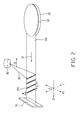
- FIGs. 1 through 4 are schematic views showing the procedure of a fabricating method of a light transmissive film according to an embodiment of the disclosure.
- FIGs. 5 and 6 are schematic views showing the procedure of a fabricating method of a light transmissive film according to another embodiment of the disclosure.
- FIGs. 7 and 8 are schematic views showing the procedure of a fabricating method of a light transmissive film according to yet another embodiment of the disclosure.
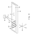
- FIG. 9 is a schematic view showing a fabricating method of a light transmissive film according to still another embodiment of the disclosure.
- FIG. 10 is a schematic view showing that the stripes are observed by a naked eye.
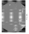
- FIG. 11 is a distribution diagram of moiré degree caused by two periodical structures at different included angles and different periodical ratios.
- FIGs. 12A through 12G are optical microscopic views of the stripes.
- FIGs. 1 through 4 are schematic views showing the procedure of a fabricating method of a light transmissive film according to an embodiment of the disclosure.
- the manufacturing method of the light transmissive film according to this embodiment includes steps as follows. Referring to FIG. 1 , first, a film 100 is provided, and the film 100 includes a plurality of nano-units and has a reference direction D1.
- the nano-units are, for example, a plurality of carbon nanotubes
- the film 100 is, for example, a carbon nanotube films.
- the nano-units may be nano-scale electrically conductive molecules or grains, e.g. nano-scale metal grains.
- the film 100 is an electrically conductive film having anisotropic impedance, and a main conductive direction (along which the impedance is smallest) of the electrically conductive film having anisotropic impedance is substantially parallel to the reference direction D1.
- the carbon nanotubes extend about along the reference direction D1.
- the step of providing the film 100 includes steps as follows. First, a carbon nanotube layer 60 is formed on a substrate 50.
- the substrate 50 is a silicon substrate, a quartz substrate, or other suitable substrates, for example.
- the carbon nanotube layer 60 is, for example, formed by chemical vapor deposition (CVD) or other suitable methods.
- CVD chemical vapor deposition
- a side of the carbon nanotube layer 60 is pulled and the carbon nanotube layer 60 is stretched along a stretching direction (i.e. the reference direction D1 in this embodiment) so as to form a stretched carbon nanotube film.
- a clip 70 is used to clip the side of the carbon nanotube film and pull out the carbon nanotube film from the substrate 50 laterally.
- the carbon nanotubes therein extend about along the reference direction D1.
- the reference direction D1 is, for example, the stretching direction of the film 100.
- the reference direction D1 may be substantially parallel to a side M of the film 100.
- the film 100 is struck by an energy beam 82 so as to form a plurality of first stripes 210 parallel to each other on the film 100, and the first stripes 210 are neither perpendicular nor parallel to the reference D1.
- the difference may be a physical difference, a structural difference, or an optical difference.
- the difference is a texture difference, a density difference of the nano-units, a difference of surface roughness, a thickness difference (i.e., the first stripes are recessed stripes), a structural difference of the nano-units (e.g.
- the extending direction L1 of the first stripes 210 is inclined with respect to a reference direction R1 by an angle ⁇ .
- the reference direction R1 is in the surface of the film 100 and perpendicular to the reference direction D1, and ⁇ is greater than 0 degree and less than 90 degrees.
- ⁇ may be less than 0 degree and greater than -90 degrees. That is to say, the inclination direction of the extending direction L1 with respect to the reference direction R1 is opposite to the direction shown by the arrow near the letter ⁇ in FIG. 2 .
- the energy beam 32 is, for example, a laser beam emitted by a laser source 80, and the wavelength thereof falls within the range of visible light, ultraviolet light, infrared light, or other electromagnetic waves, by which the disclosure is not limited.
- the energy beam 82 may be a particle beam having kinetic energy, for example, an electron beam, a proton beam, a helium nucleus beam, or other suitable particle beams.
- the step of forming the first stripes 210 by the energy beam 82 includes scanning the film 100 along a scanning direction S1 parallel to the reference direction D1 (the scanning direction S1 is opposite to the reference direction D1 in this embodiment) by the energy beam 82, so as to form the first stripes 210 in sequence.
- the first stripes 210 are periodically arranged, for example, arranged at equal intervals or arranged with other periodical forms.
- the width W of the first stripes 210 is, for example, about 110 microns, and the pitch P of the first stripes 210 falls within the range of 200 microns to 350 microns, by which the disclosure is not limited.
- the manufacturing method of the light transmissive film may include repeatedly scanning the positions of the first stripes 210 along scanning directions S1 and S2 (the scanning direction S2 is the same as the reference direction D1) parallel to the reference direction D1 by the energy beam 82, so as to enhance the difference between the first stripes 210 and the structures not struck by the energy 82 and respectively adjacent to the first stripes 210, for example, to increase the recessed depth of the first stripes 210, to increase the texture difference, to increase the density difference of the nano-units, to increase the difference of surface roughness, to increase the structural difference of the nano-units, to increase the phase difference of the nano-units, to increase the intensity difference of reflective light, to increase the intensity difference of transmissive light, or to increase the intensity difference of diffractive light.
- the scanning is performed back and forth along the scanning direction S1 and S2 alternately many times, so as to increase the recessed depth of the first stripes 210.
- the original positions of the stripes 210 formed previously may not be scanned repeatedly, but other positions shifted from the original positions are scanned.
- the stripes 210 increase the transmittance of the film 100, so as to form a light transmissive film 200 as shown in FIG. 4 .
- the light transmissive film 200 includes the plurality of nano-units and the first stripes 210 as described hereinbefore.
- the nano-units form the film 100, and the first stripes 210 are located on the surface of the film 100.
- the moiré formed by the first stripes 210 and other periodical structures is reduced or prevented by properly adjusting the extending direction L1 of the first stripes 210 (e.g. adjusting the angle ⁇ ), the width W, and the pitch P (as shown in FIG. 2 ).
- FIGs. 5 and 6 are schematic views showing the procedure of a fabricating method of a light transmissive film according to another embodiment of the disclosure.
- the manufacturing method of the light transmissive film of this embodiment is similar to the manufacturing method of the light transmissive film shown by FIGs. 1 through 4 , and the main difference therebetween is as follows.
- the manufacturing method of the light transmissive film according to this embodiment further includes forming a plurality of second stripes 220 on the surface of the film 100 by the energy beam 82, and each of the second stripes 220 is not parallel to each of the first stripes 210.
- the characteristic of the second stripes 220 is similar to that of the first stripes 210, and is not repeated herein.
- the second stripes 220 may be arranged periodically.
- the extending direction L2 of the second stripes 220 is inclined with respect to the reference direction R1 by an angle ⁇ , and ⁇ is less than 0 degree and greater than -90 degrees.
- ⁇ and ⁇ may be zero degree.
- the width and the pitch of the second stripes 220 may be about the same as the width and the pitch of the first stripes 210.
- the scanning may be performed along the scanning directions S1 and S2 back and forth many times by the energy beam 82, so as to increase the difference between the second stripes 220 and the structures respectively adjacent to the second stripes 220.
- the first stripes 210 and the second stripes 220 increase the transmittance of the film 100, so as to form a light transmissive film 200'.
- each of the first stripes 210 being not parallel to each of the second stripes 220 spoils the periodicity of each other, such that the user is not easy to observe the first stripes 210 and the second stripes 220 by naked eyes. Therefore, when the light transmissive film 200' of this embodiment is used to be an electrically conductive film of a touch panel, the quality, the brightness uniformity, and the color uniformity of displaying frames are improved. Additionally, the light transmissive film 200' according to this embodiment may be used to adhere to the windows or the heat insulating papers, such that the windows may have touch control function.
- the light transmissive film 200' may also be used to be an electrically conductive film of a flexible panel, e.g. a flexible display panel or a flexible touch display panel. Since the carbon nanotube film has better flexibility and is not easy to deteriorate due to being unduly bent or after being bent too many times, the reliability of the flexible panel is improved.
- each of the first stripes 210 being not parallel to each of the second stripes 220 spoils the periodicity of each other, such that the first stripes 210 and the second stripes 220 are not easy to cause moiré with other periodical structures, e.g. a pixel array of a display panel.
- the light transmissive film of this embodiment is used to be an electrically conductive film of a touch display panel, the quality and the uniformity of the displaying frames are improved.
- FIGs. 7 and 8 are schematic views showing the procedure of a fabricating method of a light transmissive film according to yet another embodiment of the disclosure.
- the manufacturing method of the light transmissive film of this embodiment is similar to the manufacturing method of the light transmissive film shown by FIGs. 5 and 6 , and the main difference therebetween is as follows.
- the manufacturing method of the light transmissive film according to this embodiment further includes forming a plurality of third stripes 230 on the surface of the film 100 by the energy beam 82, and each of the third stripes 230 is neither parallel to each of the first stripes 210 nor parallel to each of the second stripes 220.
- the characteristic of the third stripes 220 is similar to that of the first stripes 210 and that of the second stripes 220, and is not repeated herein.
- the third stripes 230 may be arranged periodically.
- the extending direction L3 of each of the third stripes 230 is substantially parallel to the reference direction R1, i.e. inclined with respect to the reference direction R1 by zero degree, by which the disclosure is not limited.
- the scanning may be performed along the scanning directions S1 and S2 back and forth by the energy beam 82, so as to increase the difference between the third stripes 230 and the structures respectively adjacent to the third stripes 230.
- the first stripes 210, the second stripes 220, and the third stripes 230 increase the transmittance of the film 100, so as to form a light transmissive film 200". Since the light transmissive film 200" according to this embodiment has three sets of stripes respectively having different extending directions, i.e. the first stripes 210, the second stripes 220, and the third stripes 230, the periodicity of the stripes are spoiled more. In this way, the first stripes 210, the second stripes 220, and the third stripes 230 on the light transmissive film 200" is harder to be observe by naked eyes and harder to cause moiré with other periodical structures.
- FIG. 9 is a schematic view showing a fabricating method of a light transmissive film according to still another embodiment of the disclosure.
- the manufacturing method of the light transmissive film of this embodiment is similar to the manufacturing method of the light transmissive film shown by FIGs. 1 through 4 , and the main difference therebetween is as follows.
- the stretched film 100 is disposed on a carrier 90.
- the carrier 90 is, for example, a resin or plastic substrate. After the film 100 is disposed on the carrier 90, the formation of the first stripes 210 is started.
- the reference direction D1 is substantially parallel to the side M of the film 100.
- the manufacturing method of the light transmissive film and the light transmissive film formed by this method have similar advantages and effects to those described in the above embodiments, and are not repeated herein.
- FIG. 10 is a schematic view showing that stripes are observed by a naked eye away from the stripes by a distance A.
- the naked eye when the observing solid angle ⁇ 1 of the human eye observing the stripes is less than the solid angle corresponding to the contrast sensitivity, the naked eye can not recognize the stripes.
- the observing solid angle ⁇ 1 of the human eye observing the stripes is greater than the solid angle corresponding to the contrast sensitivity, the naked eye is easier to recognize the stripes.
- the smallest solid angle at which the human eye can recognize the stripes under a certain contrast condition is compared with the observing solid angle ⁇ 1, if the observing angle ⁇ 1 is smaller, the naked eye can not recognized moiré; otherwise, the naked can recognized moiré.
- the embodiments of FIGs. 1 through 4 , and 4 reduce the degree of moiré by controlling the contrast and contrast sensitivity caused by the first stripes 210 and the width and the pitch of the first stripes 210.
- the embodiments of FIGs. 5 , 6 , 3A , and 8 adopt plural sets of stripes respectively having different extending directions to spoil the periodicity of each other.
- the naked eye is still harder to recognize moiré.
- FIG. 11 is a distribution diagram of moiré degree caused by two periodical structures at different included angles and different periodical ratios.
- the horizontal axis refers to the included angle of the two periodical structures
- the vertical axis refers to the periodical ratios between the two periodical structures.
- the numbers on the curves in FIG. 11 refers to the degree of moiré. The larger this number is, the higher the degree of moiré is.
- the relationship between the stripes of the above embodiments of the disclosure and other periodical structures, e.g. the pixel array of the display panel, may be designed to fall within the area where the above-mentioned numbers are smaller, so as to improve the quality and uniformity of the displaying frames.
- FIGs. 12A through 12G are optical microscopic views of the stripes, and the real size of the stripes can be known from the scale bars in the figures.
- FIG. 12A is a magnified view of the film when the stripes is perpendicular to the reference direction D1 of FIG. 1 .
- the stripes in FIG. 12A are rather obvious.
- the stripes are less obvious in this figure.
- the stripes are very non-obvious in this figure even though the stripes are observed by an optical microscope.
- the stripes are very non-obvious in this figure even though the stripes are observed by the optical microscope.
- FIG. 12E is a magnified view of the light transmissive
- the stripes are very non-obvious in this figure even though the stripes are observed by the optical microscope.
- the disclosure does not limit the number of sets of the stripes having different extending directions formed by the manufacturing method of the light transmissive film or owned by the light transmissive film to be three or less. In other embodiments, four sets or more of the stripes having different extending directions may be formed or used.
- the first stripes are neither perpendicular nor parallel to the reference direction, the first stripes formed by the manufacturing method of the light transmissive film and the first stripes of the light transmissive film are not easy to cause obvious moiré with other periodical structures.
- the stripes formed by the manufacturing method of the light transmissive film and the stripes of the light transmissive film are harder to recognized by the naked eye.
Abstract
Description
- The present disclosure generally relates a film and the manufacturing method thereof, and more particularly, to a light transmissive film and the manufacturing method thereof.
- Along with the development of the displaying technology and multimedia technology, the typical bottom or mouse interface has been unsatisfied for the user. Since the portable electronic device is generally used, manufacturers have been pursued a user interface which is more easy to operate and more intuitive, and occupies less space. The touch panel is one of the devices which can achieve these effects.
- The typical touch panels are generally categorized into capacitive touch panels and resistive touch panels. The resistive touch panel adopts two indium tin oxide (ITO) films. When the user presses the resistive touch panel by a finger, the two ITO films contact with and are electrically connected with each other. In this way, a processing unit can calculate the position pressed by the finger.
- The ITO film in the capacitive touch panel is divided into a plurality of patterns. When the user contacts the capacitive touch panel by a finger, the capacitance between the patterns is changed, whereby a processing unit calculates the position pressed by the finger.
- However, the patterns on the capacitive touch panel may lead the frame to be non-uniform. Besides, when the ITO film is bent unduly or bent too many times, it is easy to generate cracks on the ITO film or deteriorate the ITO film. Therefore, when the ITO film is used in a flexible panel, it is easy to decrease the reliability of the flexible panel.
- An embodiment of the disclosure provides a manufacturing method of a light transmissive film which includes following steps. A film is provided, and the film includes a plurality of nano-units and has a reference direction. In addition, a plurality of first stripes parallel to each other is formed on the film by an energy beam, and the first stripes are neither perpendicular nor parallel to the reference direction.
- Another embodiment of the disclosure provides a light transmissive film formed by the above manufacturing method of the light transmissive.
- Yet another embodiment of the disclosure provided a light transmissive film including a plurality of nano-units and a plurality of first stripes parallel to each other. The nano-units form a film. The first stripes are located on a surface of the film, and the first stripes are neither perpendicular nor parallel to a reference direction of the film.
- In order to make the aforementioned and other features and advantages of the disclosure more comprehensible, embodiments accompanying figures are described in detail below.
- The accompanying drawings are included to provide a further understanding of the disclosure, and are incorporated in and constitute a part of this specification. The drawings illustrate embodiments of the disclosure and, together with the description, serve to explain the principles of the disclosure.
-
FIGs. 1 through 4 are schematic views showing the procedure of a fabricating method of a light transmissive film according to an embodiment of the disclosure. -
FIGs. 5 and6 are schematic views showing the procedure of a fabricating method of a light transmissive film according to another embodiment of the disclosure. -
FIGs. 7 and8 are schematic views showing the procedure of a fabricating method of a light transmissive film according to yet another embodiment of the disclosure. -
FIG. 9 is a schematic view showing a fabricating method of a light transmissive film according to still another embodiment of the disclosure. -
FIG. 10 is a schematic view showing that the stripes are observed by a naked eye. -
FIG. 11 is a distribution diagram of moiré degree caused by two periodical structures at different included angles and different periodical ratios. -
FIGs. 12A through 12G are optical microscopic views of the stripes. -
FIGs. 1 through 4 are schematic views showing the procedure of a fabricating method of a light transmissive film according to an embodiment of the disclosure. The manufacturing method of the light transmissive film according to this embodiment includes steps as follows. Referring toFIG. 1 , first, afilm 100 is provided, and thefilm 100 includes a plurality of nano-units and has a reference direction D1. In this embodiment, the nano-units are, for example, a plurality of carbon nanotubes, and thefilm 100 is, for example, a carbon nanotube films. However, in other embodiments, the nano-units may be nano-scale electrically conductive molecules or grains, e.g. nano-scale metal grains. In this embodiment, from a macroscopic view, thefilm 100 is an electrically conductive film having anisotropic impedance, and a main conductive direction (along which the impedance is smallest) of the electrically conductive film having anisotropic impedance is substantially parallel to the reference direction D1. From a microscopic view, the carbon nanotubes extend about along the reference direction D1. - In this embodiment, the step of providing the
film 100 includes steps as follows. First, acarbon nanotube layer 60 is formed on asubstrate 50. Thesubstrate 50 is a silicon substrate, a quartz substrate, or other suitable substrates, for example. Thecarbon nanotube layer 60 is, for example, formed by chemical vapor deposition (CVD) or other suitable methods. Next, a side of thecarbon nanotube layer 60 is pulled and thecarbon nanotube layer 60 is stretched along a stretching direction (i.e. the reference direction D1 in this embodiment) so as to form a stretched carbon nanotube film. Specifically, aclip 70 is used to clip the side of the carbon nanotube film and pull out the carbon nanotube film from thesubstrate 50 laterally. When the carbon nanotube film is pulled out, the carbon nanotubes therein extend about along the reference direction D1. In this embodiment, the reference direction D1 is, for example, the stretching direction of thefilm 100. However, the reference direction D1 may be substantially parallel to a side M of thefilm 100. - Referring to
FIG. 2 , after that, thefilm 100 is struck by anenergy beam 82 so as to form a plurality offirst stripes 210 parallel to each other on thefilm 100, and thefirst stripes 210 are neither perpendicular nor parallel to the reference D1. There is a difference between thefirst stripes 210 and the structures not struck by theenergy beam 82 and respectively adjacent to thefirst stripes 210. The difference may be a physical difference, a structural difference, or an optical difference. For example, the difference is a texture difference, a density difference of the nano-units, a difference of surface roughness, a thickness difference (i.e., the first stripes are recessed stripes), a structural difference of the nano-units (e.g. the difference between a double wall carbon nanotube and a single wall carbon nanotube), a phase difference between the nano-units, a intensity difference of reflective light (e.g. the brightness contrast due to the reflective light from thefirst stripes 210 and the adjacent structures), a intensity difference of transmissive light (e.g. the brightness contrast due to the transmittance difference between thefirst stripes 210 and the adjacent structures), or a intensity difference of diffractive light. In this embodiment, the extending direction L1 of thefirst stripes 210 is inclined with respect to a reference direction R1 by an angle θ. The reference direction R1 is in the surface of thefilm 100 and perpendicular to the reference direction D1, and θ is greater than 0 degree and less than 90 degrees. However, in other embodiments, θ may be less than 0 degree and greater than -90 degrees. That is to say, the inclination direction of the extending direction L1 with respect to the reference direction R1 is opposite to the direction shown by the arrow near the letter θ inFIG. 2 . Theenergy beam 32 is, for example, a laser beam emitted by alaser source 80, and the wavelength thereof falls within the range of visible light, ultraviolet light, infrared light, or other electromagnetic waves, by which the disclosure is not limited. However, in other embodiments, theenergy beam 82 may be a particle beam having kinetic energy, for example, an electron beam, a proton beam, a helium nucleus beam, or other suitable particle beams. - In this embodiment, the step of forming the
first stripes 210 by theenergy beam 82 includes scanning thefilm 100 along a scanning direction S1 parallel to the reference direction D1 (the scanning direction S1 is opposite to the reference direction D1 in this embodiment) by theenergy beam 82, so as to form thefirst stripes 210 in sequence. In this embodiment, thefirst stripes 210 are periodically arranged, for example, arranged at equal intervals or arranged with other periodical forms. For example, the width W of thefirst stripes 210 is, for example, about 110 microns, and the pitch P of thefirst stripes 210 falls within the range of 200 microns to 350 microns, by which the disclosure is not limited. - Referring to
FIG. 3 , afterward, the manufacturing method of the light transmissive film may include repeatedly scanning the positions of thefirst stripes 210 along scanning directions S1 and S2 (the scanning direction S2 is the same as the reference direction D1) parallel to the reference direction D1 by theenergy beam 82, so as to enhance the difference between thefirst stripes 210 and the structures not struck by theenergy 82 and respectively adjacent to thefirst stripes 210, for example, to increase the recessed depth of thefirst stripes 210, to increase the texture difference, to increase the density difference of the nano-units, to increase the difference of surface roughness, to increase the structural difference of the nano-units, to increase the phase difference of the nano-units, to increase the intensity difference of reflective light, to increase the intensity difference of transmissive light, or to increase the intensity difference of diffractive light. In this embodiment, the scanning is performed back and forth along the scanning direction S1 and S2 alternately many times, so as to increase the recessed depth of thefirst stripes 210. However, in other embodiments, when the scanning is performed back and forth along the direction S1 and S2 alternately by theenergy beam 32, the original positions of thestripes 210 formed previously may not be scanned repeatedly, but other positions shifted from the original positions are scanned. - In this embodiment, the
stripes 210 increase the transmittance of thefilm 100, so as to form alight transmissive film 200 as shown inFIG. 4 . Specifically, thelight transmissive film 200 includes the plurality of nano-units and thefirst stripes 210 as described hereinbefore. The nano-units form thefilm 100, and thefirst stripes 210 are located on the surface of thefilm 100. - In this embodiment, since the
first stripes 210 are neither perpendicular nor parallel to the reference direction D1, the moiré formed by thefirst stripes 210 and other periodical structures, e.g. a pixel array of a display panel, is reduced or prevented by properly adjusting the extending direction L1 of the first stripes 210 (e.g. adjusting the angle θ), the width W, and the pitch P (as shown inFIG. 2 ). -
FIGs. 5 and6 are schematic views showing the procedure of a fabricating method of a light transmissive film according to another embodiment of the disclosure. The manufacturing method of the light transmissive film of this embodiment is similar to the manufacturing method of the light transmissive film shown byFIGs. 1 through 4 , and the main difference therebetween is as follows. Referring toFIG. 5 , the manufacturing method of the light transmissive film according to this embodiment further includes forming a plurality ofsecond stripes 220 on the surface of thefilm 100 by theenergy beam 82, and each of thesecond stripes 220 is not parallel to each of thefirst stripes 210. The characteristic of thesecond stripes 220 is similar to that of thefirst stripes 210, and is not repeated herein. In addition, thesecond stripes 220 may be arranged periodically. In this embodiment, the extending direction L2 of thesecond stripes 220 is inclined with respect to the reference direction R1 by an angle ϕ, and ϕ is less than 0 degree and greater than -90 degrees. However, in other embodiments, one of ϕ and θ may be zero degree. In this embodiment, the width and the pitch of thesecond stripes 220 may be about the same as the width and the pitch of thefirst stripes 210. Besides, in this embodiment, the scanning may be performed along the scanning directions S1 and S2 back and forth many times by theenergy beam 82, so as to increase the difference between thesecond stripes 220 and the structures respectively adjacent to thesecond stripes 220. - The
first stripes 210 and thesecond stripes 220 increase the transmittance of thefilm 100, so as to form a light transmissive film 200'. In this embodiment, each of thefirst stripes 210 being not parallel to each of thesecond stripes 220 spoils the periodicity of each other, such that the user is not easy to observe thefirst stripes 210 and thesecond stripes 220 by naked eyes. Therefore, when the light transmissive film 200' of this embodiment is used to be an electrically conductive film of a touch panel, the quality, the brightness uniformity, and the color uniformity of displaying frames are improved. Additionally, the light transmissive film 200' according to this embodiment may be used to adhere to the windows or the heat insulating papers, such that the windows may have touch control function. Moreover, the light transmissive film 200' according to this embodiment may also be used to be an electrically conductive film of a flexible panel, e.g. a flexible display panel or a flexible touch display panel. Since the carbon nanotube film has better flexibility and is not easy to deteriorate due to being unduly bent or after being bent too many times, the reliability of the flexible panel is improved. - Furthermore, each of the
first stripes 210 being not parallel to each of thesecond stripes 220 spoils the periodicity of each other, such that thefirst stripes 210 and thesecond stripes 220 are not easy to cause moiré with other periodical structures, e.g. a pixel array of a display panel. As such, when the light transmissive film of this embodiment is used to be an electrically conductive film of a touch display panel, the quality and the uniformity of the displaying frames are improved. -
FIGs. 7 and8 are schematic views showing the procedure of a fabricating method of a light transmissive film according to yet another embodiment of the disclosure. The manufacturing method of the light transmissive film of this embodiment is similar to the manufacturing method of the light transmissive film shown byFIGs. 5 and6 , and the main difference therebetween is as follows. Referring toFIG. 7 , the manufacturing method of the light transmissive film according to this embodiment further includes forming a plurality ofthird stripes 230 on the surface of thefilm 100 by theenergy beam 82, and each of thethird stripes 230 is neither parallel to each of thefirst stripes 210 nor parallel to each of thesecond stripes 220. The characteristic of thethird stripes 220 is similar to that of thefirst stripes 210 and that of thesecond stripes 220, and is not repeated herein. In addition, thethird stripes 230 may be arranged periodically. In this embodiment, the extending direction L3 of each of thethird stripes 230 is substantially parallel to the reference direction R1, i.e. inclined with respect to the reference direction R1 by zero degree, by which the disclosure is not limited. In this embodiment, the scanning may be performed along the scanning directions S1 and S2 back and forth by theenergy beam 82, so as to increase the difference between thethird stripes 230 and the structures respectively adjacent to thethird stripes 230. - The
first stripes 210, thesecond stripes 220, and thethird stripes 230 increase the transmittance of thefilm 100, so as to form alight transmissive film 200". Since thelight transmissive film 200" according to this embodiment has three sets of stripes respectively having different extending directions, i.e. thefirst stripes 210, thesecond stripes 220, and thethird stripes 230, the periodicity of the stripes are spoiled more. In this way, thefirst stripes 210, thesecond stripes 220, and thethird stripes 230 on thelight transmissive film 200" is harder to be observe by naked eyes and harder to cause moiré with other periodical structures. -
FIG. 9 is a schematic view showing a fabricating method of a light transmissive film according to still another embodiment of the disclosure. Referring toFIG. 9 , the manufacturing method of the light transmissive film of this embodiment is similar to the manufacturing method of the light transmissive film shown byFIGs. 1 through 4 , and the main difference therebetween is as follows. In this embodiment, before thefirst stripes 210 are formed by theenergy beam 82, the stretchedfilm 100 is disposed on acarrier 90. In this embodiment, thecarrier 90 is, for example, a resin or plastic substrate. After thefilm 100 is disposed on thecarrier 90, the formation of thefirst stripes 210 is started. In this case, the reference direction D1 is substantially parallel to the side M of thefilm 100. The manufacturing method of the light transmissive film and the light transmissive film formed by this method have similar advantages and effects to those described in the above embodiments, and are not repeated herein. -
FIG. 10 is a schematic view showing that stripes are observed by a naked eye away from the stripes by a distance A. Referring toFIG. 10 , when the observing solid angle θ1 of the human eye observing the stripes is less than the solid angle corresponding to the contrast sensitivity, the naked eye can not recognize the stripes. On the contrary, when the observing solid angle θ1 of the human eye observing the stripes is greater than the solid angle corresponding to the contrast sensitivity, the naked eye is easier to recognize the stripes. On the other hand, when the smallest solid angle at which the human eye can recognize the stripes under a certain contrast condition is compared with the observing solid angle θ1, if the observing angle θ1 is smaller, the naked eye can not recognized moiré; otherwise, the naked can recognized moiré. The formulas to calculate the contrast sensitivity function (CSF) are as follows

- where Δ/ is the difference between the largest brightness and the smallest brightness of the stripes; lave is the average brightness of the stripes; lmax is the largest brightness of the stripes; lmin is the smallest brightness of the stripes.
- Therefore, the embodiments of
FIGs. 1 through 4 , and4 reduce the degree of moiré by controlling the contrast and contrast sensitivity caused by thefirst stripes 210 and the width and the pitch of thefirst stripes 210. Moreover, the embodiments ofFIGs. 5 ,6 ,3A , and8 adopt plural sets of stripes respectively having different extending directions to spoil the periodicity of each other. As a result, even if the observing solid angle θ1 of the human eye observing one set of the stripes extending along a single direction is greater the solid angle corresponding to the contrast sensitivity, or even if the smallest solid angle at which the human eye can recognize the stripes under a certain contrast condition is smaller than the observing solid angle θ1, the naked eye is still harder to recognize moiré. -
FIG. 11 is a distribution diagram of moiré degree caused by two periodical structures at different included angles and different periodical ratios. Referring toFIG. 11 , the horizontal axis refers to the included angle of the two periodical structures, and the vertical axis refers to the periodical ratios between the two periodical structures. The numbers on the curves inFIG. 11 refers to the degree of moiré. The larger this number is, the higher the degree of moiré is. The relationship between the stripes of the above embodiments of the disclosure and other periodical structures, e.g. the pixel array of the display panel, may be designed to fall within the area where the above-mentioned numbers are smaller, so as to improve the quality and uniformity of the displaying frames. -
FIGs. 12A through 12G are optical microscopic views of the stripes, and the real size of the stripes can be known from the scale bars in the figures. Referring toFIG. 12A, FIG. 12A is a magnified view of the film when the stripes is perpendicular to the reference direction D1 ofFIG. 1 . The stripes inFIG. 12A are rather obvious. FIG. 16 is a magnified view of thelight transmissive film 200 formed in the embodiment ofFIGs. 1 through 4 , wherein θ=45 degrees. The stripes are less obvious in this figure.FIG. 12C is a magnified view of the light transmissive film 200' formed in the embodiment ofFIGs. 5 through 6 , and θ=3 degrees and ϕ=-3 degrees.FIG. 12D is a magnified view of the light transmissive film 200' formed in the embodiment ofFIGs. 5 through 6 , and θ=5 degrees and ϕ=-5 degrees.FIG. 12E is a magnified view of the light transmissive film 200' formed in the embodiment ofFIGs. 5 through 6 , and θ=8 degrees and ϕ=-8 degrees. The stripes are very non-obvious in this figure even though the stripes are observed by an optical microscope.FIG. 12F is a magnified view of the light transmissive film 200' formed in the embodiment ofFIGs. 5 through 6 , and θ=10 degrees and ϕ=-10 degrees. The stripes are very non-obvious in this figure even though the stripes are observed by the optical microscope.FIG. 12G is a magnified view of thelight transmissive film 200" formed in the embodiment ofFIGs. 7 through 8 , and θ=45 degrees, ϕ=-45 degrees, and the extending direction L3 is inclined with respect to the reference direction R1 by zero degree. The stripes are very non-obvious in this figure even though the stripes are observed by the optical microscope. - It should be noted that the disclosure does not limit the number of sets of the stripes having different extending directions formed by the manufacturing method of the light transmissive film or owned by the light transmissive film to be three or less. In other embodiments, four sets or more of the stripes having different extending directions may be formed or used.
- In view of the above, in the embodiment of the disclosure, since the first stripes are neither perpendicular nor parallel to the reference direction, the first stripes formed by the manufacturing method of the light transmissive film and the first stripes of the light transmissive film are not easy to cause obvious moiré with other periodical structures. In addition, in the embodiments of the disclosure, since two sets or more of stripes having different extending directions are formed and used to spoil the periodicity of each other, the stripes formed by the manufacturing method of the light transmissive film and the stripes of the light transmissive film are harder to recognized by the naked eye.
- Although the disclosure has been described with reference to the above embodiments, it will be apparent to one of the ordinary skill in the art that modifications to the described embodiment may be made without departing from the spirit of the disclosure. Accordingly, the scope of the disclosure will be defined by the attached claims not by the above detailed descriptions.
Claims (20)
- A manufacturing method of a light transmissive film, comprising:providing a film comprising a plurality of nano-units and having a reference direction; andforming a plurality of first stripes parallel to each other on the film by an energy beam, wherein the first stripes are neither perpendicular nor parallel to the reference direction.
- The manufacturing method according to claim 1, wherein the step of providing the film comprising stretching the film along a stretching direction, and the reference direction is the stretching direction.
- The manufacturing method according to claim 2, wherein the film is an electrically conductive film having anisotropic impedance, and a main conductive direction of the electrically conductive film having anisotropic impedance is substantially parallel to the reference direction.
- The manufacturing method according to claim 3, wherein the electrically conductive film having anisotropic impedance is a carbon nanotube film.
- The manufacturing method according to claim 4, wherein the step of providing the film comprises:forming a carbon nanotube layer on a substrate; andpulling a side of the carbon nanotube layer to stretch the carbon nanotube layer along the stretching direction so as to form the stretched carbon nanotube film.
- The manufacturing method according to claim 5, wherein the step of providing the film further comprises disposing the stretched carbon nanotube film on a carrier.
- The manufacturing method according to any preceding claim, wherein the reference direction is substantially parallel to a side of the film.
- The manufacturing method according to any preceding claim, wherein the energy beam is a laser beam or a particle beam.
- The manufacturing method according to any preceding claim, wherein the step of forming the first stripes by the energy beam comprising scanning the carbon nanotube film along a direction parallel to the reference direction by the energy beam, so as to form the first stripes in sequence.
- The manufacturing method according to claim 9, further comprising repeatedly scanning the positions of the first stripes along the direction parallel to the reference direction by the energy beam so as to enhance a difference between the first stripes and structures respectively adjacent to the first stripes.
- The manufacturing method according to any preceding claim, further comprising forming a plurality of second stripes parallel to each other on the film by the energy beam, wherein each of the second stripes is not parallel to each of the first stripes.
- The manufacturing method according to any preceding claim, wherein the first stripes are periodically arranged.
- A light transmissive film formed by the manufacturing method according to claim 1.
- A light transmissive film, comprising:a plurality of nano-units forming a film; anda plurality of first stripes parallel to each other on a surface of the film, wherein the first stripes are neither perpendicular nor parallel to a reference direction of the film.
- The light transmissive film according to claim 14, wherein the reference direction is a stretching direction of the film when the film is manufactured.
- The light transmissive film according to claim 14 or 15, wherein the reference direction is substantially parallel to a side of the film.
- The light transmissive film according to claim 14, 15 or 16, wherein the film is an electrically conductive film having anisotropic impedance, and a main conductive direction of the electrically conductive film having anisotropic impedance is substantially parallel to the reference direction.
- The light transmissive film according to claim 17, wherein the electrically conductive film having anisotropic impedance is a carbon nanotube film.
- The light transmissive film according to any of claims 14 to 18, further comprising a plurality of second stripes parallel to each other on the surface of the film, wherein each of the second stripes is not parallel to each of the first stripes.
- The light transmissive film according to any of claims 14 to 19, wherein the first stripes are periodically arranged.
Applications Claiming Priority (1)
| Application Number | Priority Date | Filing Date | Title |
|---|---|---|---|
| CN200910306923A CN102024524B (en) | 2009-09-11 | 2009-09-11 | Preparation method of transmitting film, and transmitting film |
Publications (3)
| Publication Number | Publication Date |
|---|---|
| EP2296084A2 true EP2296084A2 (en) | 2011-03-16 |
| EP2296084A3 EP2296084A3 (en) | 2012-11-21 |
| EP2296084B1 EP2296084B1 (en) | 2016-03-23 |
Family
ID=43303885
Family Applications (1)
| Application Number | Title | Priority Date | Filing Date |
|---|---|---|---|
| EP10176076.7A Active EP2296084B1 (en) | 2009-09-11 | 2010-09-09 | Light transmissive film and fabrication method of light transmissive film |
Country Status (5)
| Country | Link |
|---|---|
| US (1) | US8846175B2 (en) |
| EP (1) | EP2296084B1 (en) |
| JP (1) | JP5670677B2 (en) |
| KR (1) | KR101732908B1 (en) |
| CN (1) | CN102024524B (en) |
Families Citing this family (4)
| Publication number | Priority date | Publication date | Assignee | Title |
|---|---|---|---|---|
| KR101482401B1 (en) * | 2013-04-30 | 2015-01-13 | 삼성전기주식회사 | Display device including touch panel and Method for evaluation visibility of electorde pattern of the touch panel |
| CN108630839A (en) * | 2018-03-26 | 2018-10-09 | 广东欧珀移动通信有限公司 | Battery cover and electronic device |
| CN108391393A (en) * | 2018-03-26 | 2018-08-10 | 广东欧珀移动通信有限公司 | Protective shell and electronic building brick |
| CN108630840B (en) * | 2018-03-26 | 2021-08-06 | Oppo广东移动通信有限公司 | Battery cover and electronic device |
Family Cites Families (23)
| Publication number | Priority date | Publication date | Assignee | Title |
|---|---|---|---|---|
| JPH0760856A (en) * | 1993-08-30 | 1995-03-07 | Toray Ind Inc | Reflection-preventing article and its manufacture |
| JP2002014208A (en) * | 2000-04-26 | 2002-01-18 | Sharp Corp | Optical film, light reflecting film, liquid crystal display panel, method and apparatus for producing optical film, method for producing patterning roller, and method and apparatus for sticking optical film therefor |
| US7153592B2 (en) * | 2000-08-31 | 2006-12-26 | Fujitsu Limited | Organic EL element and method of manufacturing the same, organic EL display device using the element, organic EL material, and surface emission device and liquid crystal display device using the material |
| CA2442310A1 (en) * | 2001-03-26 | 2002-10-03 | Eikos, Inc. | Coatings containing carbon nanotubes |
| JP2004053784A (en) * | 2002-07-18 | 2004-02-19 | Sharp Corp | Liquid crystal display device and method for manufacturing the same |
| CN1281982C (en) * | 2002-09-10 | 2006-10-25 | 清华大学 | Polarized element and method for manufacturing same |
| JP2005062356A (en) * | 2003-08-08 | 2005-03-10 | Seiko Epson Corp | Method for forming pattern, method for forming wiring pattern, electro-optic apparatus and electronic appliance |
| US20050209392A1 (en) * | 2003-12-17 | 2005-09-22 | Jiazhong Luo | Polymer binders for flexible and transparent conductive coatings containing carbon nanotubes |
| WO2006026743A1 (en) | 2004-08-31 | 2006-03-09 | Fusion Optix, Inc. | Enhanced light diffusing sheet |
| JP4778261B2 (en) * | 2005-04-26 | 2011-09-21 | 日本電気株式会社 | Display device and terminal device |
| JP2007065160A (en) * | 2005-08-30 | 2007-03-15 | Keiwa Inc | Substrate film for optical sheet, optical sheet and backlight unit |
| JP2007334150A (en) * | 2006-06-16 | 2007-12-27 | Fujifilm Corp | Polarizing film for window and front window for vehicle |
| US20080024870A1 (en) * | 2006-07-27 | 2008-01-31 | Bourdelais Robert P | Light-redirecting film containing optical modification layer |
| TWI317025B (en) * | 2006-08-28 | 2009-11-11 | Eternal Chemical Co Ltd | Optical film |
| US20080152870A1 (en) * | 2006-12-22 | 2008-06-26 | Katsunori Takada | Transparent electrically-conductive hard-coated substrate and method for producing the same |
| US7530726B2 (en) * | 2007-03-06 | 2009-05-12 | Skc Haas Display Films Co., Ltd. | Light redirecting film having discontinuous coating |
| CN101470558B (en) * | 2007-12-27 | 2012-11-21 | 清华大学 | Touch screen and display equipment |
| CN101458975B (en) * | 2007-12-12 | 2012-05-16 | 清华大学 | Electronic element |
| EP2071438A3 (en) * | 2007-12-14 | 2011-04-27 | Tsing Hua University | Touch panel and display device using the same |
| CN101458607B (en) * | 2007-12-14 | 2010-12-29 | 清华大学 | Touch screen and display device |
| JP2009198638A (en) * | 2008-02-20 | 2009-09-03 | Seiko Epson Corp | Wire grid type polarizing element, method for manufacturing the same, electrooptical apparatus and projection type display apparatus |
| WO2009107846A1 (en) | 2008-02-29 | 2009-09-03 | 独立行政法人産業技術総合研究所 | Carbon nanotube film structure and method for manufacturing the same |
| JP5335401B2 (en) * | 2008-12-19 | 2013-11-06 | 富士フイルム株式会社 | Polarizing film, polarizing film manufacturing method, polarizing plate, polarizing plate manufacturing method, and anti-reflection film for vehicle |
-
2009
- 2009-09-11 CN CN200910306923A patent/CN102024524B/en active Active
-
2010
- 2010-08-09 US US12/852,527 patent/US8846175B2/en active Active
- 2010-08-19 KR KR1020100080238A patent/KR101732908B1/en active IP Right Grant
- 2010-09-08 JP JP2010200760A patent/JP5670677B2/en active Active
- 2010-09-09 EP EP10176076.7A patent/EP2296084B1/en active Active
Non-Patent Citations (1)
| Title |
|---|
| None |
Also Published As
| Publication number | Publication date |
|---|---|
| EP2296084A3 (en) | 2012-11-21 |
| KR101732908B1 (en) | 2017-05-08 |
| CN102024524B (en) | 2012-08-29 |
| JP2011056948A (en) | 2011-03-24 |
| JP5670677B2 (en) | 2015-02-18 |
| US20110064910A1 (en) | 2011-03-17 |
| EP2296084B1 (en) | 2016-03-23 |
| KR20110028218A (en) | 2011-03-17 |
| US8846175B2 (en) | 2014-09-30 |
| CN102024524A (en) | 2011-04-20 |
Similar Documents
| Publication | Publication Date | Title |
|---|---|---|
| US10901563B2 (en) | Touch panel sensor, touch panel device and display device | |
| JP6280255B2 (en) | Patterned substrate with non-linear conductor traces | |
| US8970515B2 (en) | Touch screen sensor and patterned substrate having overlaid micropatterns with low visibility | |
| TWI596518B (en) | Touch screen sensor, image display device including the same, and fabricating method thereof | |
| US20120307364A1 (en) | Reducing Optical Effects in a Display | |
| US20140356584A1 (en) | Transparent conductive film | |
| TWI570749B (en) | Transparent conductive element and method of manufacturing the same, input device, electronic machine, and transparent conductive layer processing method | |
| JP2013048114A (en) | Edge shadow reducing method for prismatic front light | |
| EP2296084A2 (en) | Light transmissive film and fabrication method of light transmissive film | |
| US20130004709A1 (en) | Transparent electrode device, information input device, and electronic equipment | |
| JP2014026510A (en) | Electrode substrate for touch panel, touch panel, and image display device | |
| KR101555080B1 (en) | Touch sensor intergrated with a polarizer and display device comprising the same | |
| KR102424650B1 (en) | A conductive member, a conductive film, a display device including the same, a touch panel, a method for producing a wiring pattern for a conductive member, and a method for producing a wiring pattern for a conductive film | |
| JP2014186687A (en) | Electrode substrate for touch panel, touch panel and image display device | |
| JP6465393B2 (en) | Manufacturing method of conductive pattern sheet, conductive pattern sheet, touch panel sensor and conductive mask provided with conductive pattern sheet | |
| KR20140087761A (en) | Touch Panel | |
| TWI412780B (en) | Light transmissive film and fabrication method of light transmissive film | |
| KR102337893B1 (en) | High resolution touch sensor | |
| JP2012181245A (en) | Display element and display device | |
| CN113961091A (en) | Method to design low visibility metal grid touch sensors | |
| JP2014026485A (en) | Electrode substrate for touch panel, touch panel, and image display device |
Legal Events
| Date | Code | Title | Description |
|---|---|---|---|
| PUAI | Public reference made under article 153(3) epc to a published international application that has entered the european phase |
Free format text: ORIGINAL CODE: 0009012 |
|
| AK | Designated contracting states |
Kind code of ref document: A2 Designated state(s): AL AT BE BG CH CY CZ DE DK EE ES FI FR GB GR HR HU IE IS IT LI LT LU LV MC MK MT NL NO PL PT RO SE SI SK SM TR |
|
| AX | Request for extension of the european patent |
Extension state: BA ME RS |
|
| RIN1 | Information on inventor provided before grant (corrected) |
Inventor name: HSU, YU-JU |
|
| PUAL | Search report despatched |
Free format text: ORIGINAL CODE: 0009013 |
|
| AK | Designated contracting states |
Kind code of ref document: A3 Designated state(s): AL AT BE BG CH CY CZ DE DK EE ES FI FR GB GR HR HU IE IS IT LI LT LU LV MC MK MT NL NO PL PT RO SE SI SK SM TR |
|
| AX | Request for extension of the european patent |
Extension state: BA ME RS |
|
| RIC1 | Information provided on ipc code assigned before grant |
Ipc: G06F 3/044 20060101AFI20121016BHEP |
|
| 17P | Request for examination filed |
Effective date: 20130521 |
|
| GRAP | Despatch of communication of intention to grant a patent |
Free format text: ORIGINAL CODE: EPIDOSNIGR1 |
|
| INTG | Intention to grant announced |
Effective date: 20150923 |
|
| GRAS | Grant fee paid |
Free format text: ORIGINAL CODE: EPIDOSNIGR3 |
|
| GRAA | (expected) grant |
Free format text: ORIGINAL CODE: 0009210 |
|
| RAP1 | Party data changed (applicant data changed or rights of an application transferred) |
Owner name: INNOLUX CORPORATION |
|
| AK | Designated contracting states |
Kind code of ref document: B1 Designated state(s): AL AT BE BG CH CY CZ DE DK EE ES FI FR GB GR HR HU IE IS IT LI LT LU LV MC MK MT NL NO PL PT RO SE SI SK SM TR |
|
| REG | Reference to a national code |
Ref country code: GB Ref legal event code: FG4D |
|
| REG | Reference to a national code |
Ref country code: CH Ref legal event code: EP |
|
| REG | Reference to a national code |
Ref country code: AT Ref legal event code: REF Ref document number: 783757 Country of ref document: AT Kind code of ref document: T Effective date: 20160415 |
|
| REG | Reference to a national code |
Ref country code: IE Ref legal event code: FG4D |
|
| REG | Reference to a national code |
Ref country code: DE Ref legal event code: R096 Ref document number: 602010031365 Country of ref document: DE |
|
| REG | Reference to a national code |
Ref country code: DE Ref legal event code: R082 Ref document number: 602010031365 Country of ref document: DE |
|
| REG | Reference to a national code |
Ref country code: LT Ref legal event code: MG4D |
|
| REG | Reference to a national code |
Ref country code: NL Ref legal event code: MP Effective date: 20160323 |
|
| PG25 | Lapsed in a contracting state [announced via postgrant information from national office to epo] |
Ref country code: GR Free format text: LAPSE BECAUSE OF FAILURE TO SUBMIT A TRANSLATION OF THE DESCRIPTION OR TO PAY THE FEE WITHIN THE PRESCRIBED TIME-LIMIT Effective date: 20160624 Ref country code: NO Free format text: LAPSE BECAUSE OF FAILURE TO SUBMIT A TRANSLATION OF THE DESCRIPTION OR TO PAY THE FEE WITHIN THE PRESCRIBED TIME-LIMIT Effective date: 20160623 Ref country code: FI Free format text: LAPSE BECAUSE OF FAILURE TO SUBMIT A TRANSLATION OF THE DESCRIPTION OR TO PAY THE FEE WITHIN THE PRESCRIBED TIME-LIMIT Effective date: 20160323 |
|
| REG | Reference to a national code |
Ref country code: AT Ref legal event code: MK05 Ref document number: 783757 Country of ref document: AT Kind code of ref document: T Effective date: 20160323 |
|
| REG | Reference to a national code |
Ref country code: FR Ref legal event code: PLFP Year of fee payment: 7 |
|
| PG25 | Lapsed in a contracting state [announced via postgrant information from national office to epo] |
Ref country code: LV Free format text: LAPSE BECAUSE OF FAILURE TO SUBMIT A TRANSLATION OF THE DESCRIPTION OR TO PAY THE FEE WITHIN THE PRESCRIBED TIME-LIMIT Effective date: 20160323 Ref country code: LT Free format text: LAPSE BECAUSE OF FAILURE TO SUBMIT A TRANSLATION OF THE DESCRIPTION OR TO PAY THE FEE WITHIN THE PRESCRIBED TIME-LIMIT Effective date: 20160323 Ref country code: SE Free format text: LAPSE BECAUSE OF FAILURE TO SUBMIT A TRANSLATION OF THE DESCRIPTION OR TO PAY THE FEE WITHIN THE PRESCRIBED TIME-LIMIT Effective date: 20160323 Ref country code: NL Free format text: LAPSE BECAUSE OF FAILURE TO SUBMIT A TRANSLATION OF THE DESCRIPTION OR TO PAY THE FEE WITHIN THE PRESCRIBED TIME-LIMIT Effective date: 20160323 |
|
| PG25 | Lapsed in a contracting state [announced via postgrant information from national office to epo] |
Ref country code: PL Free format text: LAPSE BECAUSE OF FAILURE TO SUBMIT A TRANSLATION OF THE DESCRIPTION OR TO PAY THE FEE WITHIN THE PRESCRIBED TIME-LIMIT Effective date: 20160323 Ref country code: IS Free format text: LAPSE BECAUSE OF FAILURE TO SUBMIT A TRANSLATION OF THE DESCRIPTION OR TO PAY THE FEE WITHIN THE PRESCRIBED TIME-LIMIT Effective date: 20160723 Ref country code: EE Free format text: LAPSE BECAUSE OF FAILURE TO SUBMIT A TRANSLATION OF THE DESCRIPTION OR TO PAY THE FEE WITHIN THE PRESCRIBED TIME-LIMIT Effective date: 20160323 |
|
| PG25 | Lapsed in a contracting state [announced via postgrant information from national office to epo] |
Ref country code: RO Free format text: LAPSE BECAUSE OF FAILURE TO SUBMIT A TRANSLATION OF THE DESCRIPTION OR TO PAY THE FEE WITHIN THE PRESCRIBED TIME-LIMIT Effective date: 20160323 Ref country code: SK Free format text: LAPSE BECAUSE OF FAILURE TO SUBMIT A TRANSLATION OF THE DESCRIPTION OR TO PAY THE FEE WITHIN THE PRESCRIBED TIME-LIMIT Effective date: 20160323 Ref country code: PT Free format text: LAPSE BECAUSE OF FAILURE TO SUBMIT A TRANSLATION OF THE DESCRIPTION OR TO PAY THE FEE WITHIN THE PRESCRIBED TIME-LIMIT Effective date: 20160725 Ref country code: AT Free format text: LAPSE BECAUSE OF FAILURE TO SUBMIT A TRANSLATION OF THE DESCRIPTION OR TO PAY THE FEE WITHIN THE PRESCRIBED TIME-LIMIT Effective date: 20160323 Ref country code: CZ Free format text: LAPSE BECAUSE OF FAILURE TO SUBMIT A TRANSLATION OF THE DESCRIPTION OR TO PAY THE FEE WITHIN THE PRESCRIBED TIME-LIMIT Effective date: 20160323 Ref country code: SM Free format text: LAPSE BECAUSE OF FAILURE TO SUBMIT A TRANSLATION OF THE DESCRIPTION OR TO PAY THE FEE WITHIN THE PRESCRIBED TIME-LIMIT Effective date: 20160323 Ref country code: ES Free format text: LAPSE BECAUSE OF FAILURE TO SUBMIT A TRANSLATION OF THE DESCRIPTION OR TO PAY THE FEE WITHIN THE PRESCRIBED TIME-LIMIT Effective date: 20160323 |
|
| PG25 | Lapsed in a contracting state [announced via postgrant information from national office to epo] |
Ref country code: BE Free format text: LAPSE BECAUSE OF FAILURE TO SUBMIT A TRANSLATION OF THE DESCRIPTION OR TO PAY THE FEE WITHIN THE PRESCRIBED TIME-LIMIT Effective date: 20160323 Ref country code: IT Free format text: LAPSE BECAUSE OF FAILURE TO SUBMIT A TRANSLATION OF THE DESCRIPTION OR TO PAY THE FEE WITHIN THE PRESCRIBED TIME-LIMIT Effective date: 20160323 |
|
| REG | Reference to a national code |
Ref country code: DE Ref legal event code: R097 Ref document number: 602010031365 Country of ref document: DE |
|
| PLBE | No opposition filed within time limit |
Free format text: ORIGINAL CODE: 0009261 |
|
| STAA | Information on the status of an ep patent application or granted ep patent |
Free format text: STATUS: NO OPPOSITION FILED WITHIN TIME LIMIT |
|
| PG25 | Lapsed in a contracting state [announced via postgrant information from national office to epo] |
Ref country code: DK Free format text: LAPSE BECAUSE OF FAILURE TO SUBMIT A TRANSLATION OF THE DESCRIPTION OR TO PAY THE FEE WITHIN THE PRESCRIBED TIME-LIMIT Effective date: 20160323 |
|
| PG25 | Lapsed in a contracting state [announced via postgrant information from national office to epo] |
Ref country code: BG Free format text: LAPSE BECAUSE OF FAILURE TO SUBMIT A TRANSLATION OF THE DESCRIPTION OR TO PAY THE FEE WITHIN THE PRESCRIBED TIME-LIMIT Effective date: 20160623 |
|
| 26N | No opposition filed |
Effective date: 20170102 |
|
| PG25 | Lapsed in a contracting state [announced via postgrant information from national office to epo] |
Ref country code: MC Free format text: LAPSE BECAUSE OF FAILURE TO SUBMIT A TRANSLATION OF THE DESCRIPTION OR TO PAY THE FEE WITHIN THE PRESCRIBED TIME-LIMIT Effective date: 20160323 |
|
| REG | Reference to a national code |
Ref country code: CH Ref legal event code: PL |
|
| PG25 | Lapsed in a contracting state [announced via postgrant information from national office to epo] |
Ref country code: SI Free format text: LAPSE BECAUSE OF FAILURE TO SUBMIT A TRANSLATION OF THE DESCRIPTION OR TO PAY THE FEE WITHIN THE PRESCRIBED TIME-LIMIT Effective date: 20160323 |
|
| REG | Reference to a national code |
Ref country code: IE Ref legal event code: MM4A |
|
| PG25 | Lapsed in a contracting state [announced via postgrant information from national office to epo] |
Ref country code: IE Free format text: LAPSE BECAUSE OF NON-PAYMENT OF DUE FEES Effective date: 20160909 Ref country code: CH Free format text: LAPSE BECAUSE OF NON-PAYMENT OF DUE FEES Effective date: 20160930 Ref country code: LI Free format text: LAPSE BECAUSE OF NON-PAYMENT OF DUE FEES Effective date: 20160930 |
|
| REG | Reference to a national code |
Ref country code: FR Ref legal event code: PLFP Year of fee payment: 8 |
|
| PG25 | Lapsed in a contracting state [announced via postgrant information from national office to epo] |
Ref country code: LU Free format text: LAPSE BECAUSE OF NON-PAYMENT OF DUE FEES Effective date: 20160909 |
|
| PG25 | Lapsed in a contracting state [announced via postgrant information from national office to epo] |
Ref country code: CY Free format text: LAPSE BECAUSE OF FAILURE TO SUBMIT A TRANSLATION OF THE DESCRIPTION OR TO PAY THE FEE WITHIN THE PRESCRIBED TIME-LIMIT Effective date: 20160323 Ref country code: HU Free format text: LAPSE BECAUSE OF FAILURE TO SUBMIT A TRANSLATION OF THE DESCRIPTION OR TO PAY THE FEE WITHIN THE PRESCRIBED TIME-LIMIT; INVALID AB INITIO Effective date: 20100909 |
|
| PG25 | Lapsed in a contracting state [announced via postgrant information from national office to epo] |
Ref country code: TR Free format text: LAPSE BECAUSE OF FAILURE TO SUBMIT A TRANSLATION OF THE DESCRIPTION OR TO PAY THE FEE WITHIN THE PRESCRIBED TIME-LIMIT Effective date: 20160323 Ref country code: MT Free format text: LAPSE BECAUSE OF NON-PAYMENT OF DUE FEES Effective date: 20160930 Ref country code: HR Free format text: LAPSE BECAUSE OF FAILURE TO SUBMIT A TRANSLATION OF THE DESCRIPTION OR TO PAY THE FEE WITHIN THE PRESCRIBED TIME-LIMIT Effective date: 20160323 Ref country code: MK Free format text: LAPSE BECAUSE OF FAILURE TO SUBMIT A TRANSLATION OF THE DESCRIPTION OR TO PAY THE FEE WITHIN THE PRESCRIBED TIME-LIMIT Effective date: 20160323 |
|
| REG | Reference to a national code |
Ref country code: FR Ref legal event code: PLFP Year of fee payment: 9 |
|
| PG25 | Lapsed in a contracting state [announced via postgrant information from national office to epo] |
Ref country code: AL Free format text: LAPSE BECAUSE OF FAILURE TO SUBMIT A TRANSLATION OF THE DESCRIPTION OR TO PAY THE FEE WITHIN THE PRESCRIBED TIME-LIMIT Effective date: 20160323 |
|
| PGFP | Annual fee paid to national office [announced via postgrant information from national office to epo] |
Ref country code: GB Payment date: 20230907 Year of fee payment: 14 |
|
| PGFP | Annual fee paid to national office [announced via postgrant information from national office to epo] |
Ref country code: FR Payment date: 20230911 Year of fee payment: 14 Ref country code: DE Payment date: 20230912 Year of fee payment: 14 |