EP2295386A1 - Glass texturing - Google Patents
Glass texturing Download PDFInfo
- Publication number
- EP2295386A1 EP2295386A1 EP10186992A EP10186992A EP2295386A1 EP 2295386 A1 EP2295386 A1 EP 2295386A1 EP 10186992 A EP10186992 A EP 10186992A EP 10186992 A EP10186992 A EP 10186992A EP 2295386 A1 EP2295386 A1 EP 2295386A1
- Authority
- EP
- European Patent Office
- Prior art keywords
- glass
- film
- textured
- glass surface
- reaction products
- Prior art date
- Legal status (The legal status is an assumption and is not a legal conclusion. Google has not performed a legal analysis and makes no representation as to the accuracy of the status listed.)
- Granted
Links
Images

Classifications
-
- C—CHEMISTRY; METALLURGY
- C03—GLASS; MINERAL OR SLAG WOOL
- C03C—CHEMICAL COMPOSITION OF GLASSES, GLAZES OR VITREOUS ENAMELS; SURFACE TREATMENT OF GLASS; SURFACE TREATMENT OF FIBRES OR FILAMENTS MADE FROM GLASS, MINERALS OR SLAGS; JOINING GLASS TO GLASS OR OTHER MATERIALS
- C03C17/00—Surface treatment of glass, not in the form of fibres or filaments, by coating
- C03C17/34—Surface treatment of glass, not in the form of fibres or filaments, by coating with at least two coatings having different compositions
- C03C17/36—Surface treatment of glass, not in the form of fibres or filaments, by coating with at least two coatings having different compositions at least one coating being a metal
-
- C—CHEMISTRY; METALLURGY
- C03—GLASS; MINERAL OR SLAG WOOL
- C03C—CHEMICAL COMPOSITION OF GLASSES, GLAZES OR VITREOUS ENAMELS; SURFACE TREATMENT OF GLASS; SURFACE TREATMENT OF FIBRES OR FILAMENTS MADE FROM GLASS, MINERALS OR SLAGS; JOINING GLASS TO GLASS OR OTHER MATERIALS
- C03C17/00—Surface treatment of glass, not in the form of fibres or filaments, by coating
- C03C17/06—Surface treatment of glass, not in the form of fibres or filaments, by coating with metals
- C03C17/09—Surface treatment of glass, not in the form of fibres or filaments, by coating with metals by deposition from the vapour phase
-
- C—CHEMISTRY; METALLURGY
- C03—GLASS; MINERAL OR SLAG WOOL
- C03C—CHEMICAL COMPOSITION OF GLASSES, GLAZES OR VITREOUS ENAMELS; SURFACE TREATMENT OF GLASS; SURFACE TREATMENT OF FIBRES OR FILAMENTS MADE FROM GLASS, MINERALS OR SLAGS; JOINING GLASS TO GLASS OR OTHER MATERIALS
- C03C17/00—Surface treatment of glass, not in the form of fibres or filaments, by coating
- C03C17/22—Surface treatment of glass, not in the form of fibres or filaments, by coating with other inorganic material
-
- C—CHEMISTRY; METALLURGY
- C03—GLASS; MINERAL OR SLAG WOOL
- C03C—CHEMICAL COMPOSITION OF GLASSES, GLAZES OR VITREOUS ENAMELS; SURFACE TREATMENT OF GLASS; SURFACE TREATMENT OF FIBRES OR FILAMENTS MADE FROM GLASS, MINERALS OR SLAGS; JOINING GLASS TO GLASS OR OTHER MATERIALS
- C03C17/00—Surface treatment of glass, not in the form of fibres or filaments, by coating
- C03C17/34—Surface treatment of glass, not in the form of fibres or filaments, by coating with at least two coatings having different compositions
- C03C17/3411—Surface treatment of glass, not in the form of fibres or filaments, by coating with at least two coatings having different compositions with at least two coatings of inorganic materials
- C03C17/3429—Surface treatment of glass, not in the form of fibres or filaments, by coating with at least two coatings having different compositions with at least two coatings of inorganic materials at least one of the coatings being a non-oxide coating
- C03C17/3435—Surface treatment of glass, not in the form of fibres or filaments, by coating with at least two coatings having different compositions with at least two coatings of inorganic materials at least one of the coatings being a non-oxide coating comprising a nitride, oxynitride, boronitride or carbonitride
-
- C—CHEMISTRY; METALLURGY
- C03—GLASS; MINERAL OR SLAG WOOL
- C03C—CHEMICAL COMPOSITION OF GLASSES, GLAZES OR VITREOUS ENAMELS; SURFACE TREATMENT OF GLASS; SURFACE TREATMENT OF FIBRES OR FILAMENTS MADE FROM GLASS, MINERALS OR SLAGS; JOINING GLASS TO GLASS OR OTHER MATERIALS
- C03C17/00—Surface treatment of glass, not in the form of fibres or filaments, by coating
- C03C17/34—Surface treatment of glass, not in the form of fibres or filaments, by coating with at least two coatings having different compositions
- C03C17/3411—Surface treatment of glass, not in the form of fibres or filaments, by coating with at least two coatings having different compositions with at least two coatings of inorganic materials
- C03C17/3429—Surface treatment of glass, not in the form of fibres or filaments, by coating with at least two coatings having different compositions with at least two coatings of inorganic materials at least one of the coatings being a non-oxide coating
- C03C17/3482—Surface treatment of glass, not in the form of fibres or filaments, by coating with at least two coatings having different compositions with at least two coatings of inorganic materials at least one of the coatings being a non-oxide coating comprising silicon, hydrogenated silicon or a silicide
-
- C—CHEMISTRY; METALLURGY
- C03—GLASS; MINERAL OR SLAG WOOL
- C03C—CHEMICAL COMPOSITION OF GLASSES, GLAZES OR VITREOUS ENAMELS; SURFACE TREATMENT OF GLASS; SURFACE TREATMENT OF FIBRES OR FILAMENTS MADE FROM GLASS, MINERALS OR SLAGS; JOINING GLASS TO GLASS OR OTHER MATERIALS
- C03C17/00—Surface treatment of glass, not in the form of fibres or filaments, by coating
- C03C17/34—Surface treatment of glass, not in the form of fibres or filaments, by coating with at least two coatings having different compositions
- C03C17/36—Surface treatment of glass, not in the form of fibres or filaments, by coating with at least two coatings having different compositions at least one coating being a metal
- C03C17/3602—Surface treatment of glass, not in the form of fibres or filaments, by coating with at least two coatings having different compositions at least one coating being a metal the metal being present as a layer
- C03C17/3607—Coatings of the type glass/inorganic compound/metal
-
- C—CHEMISTRY; METALLURGY
- C03—GLASS; MINERAL OR SLAG WOOL
- C03C—CHEMICAL COMPOSITION OF GLASSES, GLAZES OR VITREOUS ENAMELS; SURFACE TREATMENT OF GLASS; SURFACE TREATMENT OF FIBRES OR FILAMENTS MADE FROM GLASS, MINERALS OR SLAGS; JOINING GLASS TO GLASS OR OTHER MATERIALS
- C03C17/00—Surface treatment of glass, not in the form of fibres or filaments, by coating
- C03C17/34—Surface treatment of glass, not in the form of fibres or filaments, by coating with at least two coatings having different compositions
- C03C17/36—Surface treatment of glass, not in the form of fibres or filaments, by coating with at least two coatings having different compositions at least one coating being a metal
- C03C17/3602—Surface treatment of glass, not in the form of fibres or filaments, by coating with at least two coatings having different compositions at least one coating being a metal the metal being present as a layer
- C03C17/3626—Surface treatment of glass, not in the form of fibres or filaments, by coating with at least two coatings having different compositions at least one coating being a metal the metal being present as a layer one layer at least containing a nitride, oxynitride, boronitride or carbonitride
-
- C—CHEMISTRY; METALLURGY
- C03—GLASS; MINERAL OR SLAG WOOL
- C03C—CHEMICAL COMPOSITION OF GLASSES, GLAZES OR VITREOUS ENAMELS; SURFACE TREATMENT OF GLASS; SURFACE TREATMENT OF FIBRES OR FILAMENTS MADE FROM GLASS, MINERALS OR SLAGS; JOINING GLASS TO GLASS OR OTHER MATERIALS
- C03C17/00—Surface treatment of glass, not in the form of fibres or filaments, by coating
- C03C17/34—Surface treatment of glass, not in the form of fibres or filaments, by coating with at least two coatings having different compositions
- C03C17/36—Surface treatment of glass, not in the form of fibres or filaments, by coating with at least two coatings having different compositions at least one coating being a metal
- C03C17/3602—Surface treatment of glass, not in the form of fibres or filaments, by coating with at least two coatings having different compositions at least one coating being a metal the metal being present as a layer
- C03C17/3636—Surface treatment of glass, not in the form of fibres or filaments, by coating with at least two coatings having different compositions at least one coating being a metal the metal being present as a layer one layer at least containing silicon, hydrogenated silicon or a silicide
-
- C—CHEMISTRY; METALLURGY
- C03—GLASS; MINERAL OR SLAG WOOL
- C03C—CHEMICAL COMPOSITION OF GLASSES, GLAZES OR VITREOUS ENAMELS; SURFACE TREATMENT OF GLASS; SURFACE TREATMENT OF FIBRES OR FILAMENTS MADE FROM GLASS, MINERALS OR SLAGS; JOINING GLASS TO GLASS OR OTHER MATERIALS
- C03C17/00—Surface treatment of glass, not in the form of fibres or filaments, by coating
- C03C17/34—Surface treatment of glass, not in the form of fibres or filaments, by coating with at least two coatings having different compositions
- C03C17/36—Surface treatment of glass, not in the form of fibres or filaments, by coating with at least two coatings having different compositions at least one coating being a metal
- C03C17/3602—Surface treatment of glass, not in the form of fibres or filaments, by coating with at least two coatings having different compositions at least one coating being a metal the metal being present as a layer
- C03C17/3649—Surface treatment of glass, not in the form of fibres or filaments, by coating with at least two coatings having different compositions at least one coating being a metal the metal being present as a layer made of metals other than silver
-
- C—CHEMISTRY; METALLURGY
- C03—GLASS; MINERAL OR SLAG WOOL
- C03C—CHEMICAL COMPOSITION OF GLASSES, GLAZES OR VITREOUS ENAMELS; SURFACE TREATMENT OF GLASS; SURFACE TREATMENT OF FIBRES OR FILAMENTS MADE FROM GLASS, MINERALS OR SLAGS; JOINING GLASS TO GLASS OR OTHER MATERIALS
- C03C17/00—Surface treatment of glass, not in the form of fibres or filaments, by coating
- C03C17/34—Surface treatment of glass, not in the form of fibres or filaments, by coating with at least two coatings having different compositions
- C03C17/36—Surface treatment of glass, not in the form of fibres or filaments, by coating with at least two coatings having different compositions at least one coating being a metal
- C03C17/3602—Surface treatment of glass, not in the form of fibres or filaments, by coating with at least two coatings having different compositions at least one coating being a metal the metal being present as a layer
- C03C17/3668—Surface treatment of glass, not in the form of fibres or filaments, by coating with at least two coatings having different compositions at least one coating being a metal the metal being present as a layer the multilayer coating having electrical properties
- C03C17/3678—Surface treatment of glass, not in the form of fibres or filaments, by coating with at least two coatings having different compositions at least one coating being a metal the metal being present as a layer the multilayer coating having electrical properties specially adapted for use in solar cells
-
- H—ELECTRICITY
- H10—SEMICONDUCTOR DEVICES; ELECTRIC SOLID-STATE DEVICES NOT OTHERWISE PROVIDED FOR
- H10F—INORGANIC SEMICONDUCTOR DEVICES SENSITIVE TO INFRARED RADIATION, LIGHT, ELECTROMAGNETIC RADIATION OF SHORTER WAVELENGTH OR CORPUSCULAR RADIATION
- H10F77/00—Constructional details of devices covered by this subclass
- H10F77/70—Surface textures, e.g. pyramid structures
- H10F77/707—Surface textures, e.g. pyramid structures of the substrates or of layers on substrates, e.g. textured ITO layer on a glass substrate
-
- C—CHEMISTRY; METALLURGY
- C03—GLASS; MINERAL OR SLAG WOOL
- C03C—CHEMICAL COMPOSITION OF GLASSES, GLAZES OR VITREOUS ENAMELS; SURFACE TREATMENT OF GLASS; SURFACE TREATMENT OF FIBRES OR FILAMENTS MADE FROM GLASS, MINERALS OR SLAGS; JOINING GLASS TO GLASS OR OTHER MATERIALS
- C03C2204/00—Glasses, glazes or enamels with special properties
- C03C2204/08—Glass having a rough surface
-
- C—CHEMISTRY; METALLURGY
- C03—GLASS; MINERAL OR SLAG WOOL
- C03C—CHEMICAL COMPOSITION OF GLASSES, GLAZES OR VITREOUS ENAMELS; SURFACE TREATMENT OF GLASS; SURFACE TREATMENT OF FIBRES OR FILAMENTS MADE FROM GLASS, MINERALS OR SLAGS; JOINING GLASS TO GLASS OR OTHER MATERIALS
- C03C2217/00—Coatings on glass
- C03C2217/20—Materials for coating a single layer on glass
- C03C2217/25—Metals
- C03C2217/251—Al, Cu, Mg or noble metals
- C03C2217/252—Al
-
- C—CHEMISTRY; METALLURGY
- C03—GLASS; MINERAL OR SLAG WOOL
- C03C—CHEMICAL COMPOSITION OF GLASSES, GLAZES OR VITREOUS ENAMELS; SURFACE TREATMENT OF GLASS; SURFACE TREATMENT OF FIBRES OR FILAMENTS MADE FROM GLASS, MINERALS OR SLAGS; JOINING GLASS TO GLASS OR OTHER MATERIALS
- C03C2217/00—Coatings on glass
- C03C2217/20—Materials for coating a single layer on glass
- C03C2217/28—Other inorganic materials
- C03C2217/282—Carbides, silicides
-
- C—CHEMISTRY; METALLURGY
- C03—GLASS; MINERAL OR SLAG WOOL
- C03C—CHEMICAL COMPOSITION OF GLASSES, GLAZES OR VITREOUS ENAMELS; SURFACE TREATMENT OF GLASS; SURFACE TREATMENT OF FIBRES OR FILAMENTS MADE FROM GLASS, MINERALS OR SLAGS; JOINING GLASS TO GLASS OR OTHER MATERIALS
- C03C2218/00—Methods for coating glass
- C03C2218/10—Deposition methods
- C03C2218/15—Deposition methods from the vapour phase
- C03C2218/151—Deposition methods from the vapour phase by vacuum evaporation
-
- C—CHEMISTRY; METALLURGY
- C03—GLASS; MINERAL OR SLAG WOOL
- C03C—CHEMICAL COMPOSITION OF GLASSES, GLAZES OR VITREOUS ENAMELS; SURFACE TREATMENT OF GLASS; SURFACE TREATMENT OF FIBRES OR FILAMENTS MADE FROM GLASS, MINERALS OR SLAGS; JOINING GLASS TO GLASS OR OTHER MATERIALS
- C03C2218/00—Methods for coating glass
- C03C2218/10—Deposition methods
- C03C2218/15—Deposition methods from the vapour phase
- C03C2218/152—Deposition methods from the vapour phase by cvd
- C03C2218/153—Deposition methods from the vapour phase by cvd by plasma-enhanced cvd
-
- C—CHEMISTRY; METALLURGY
- C03—GLASS; MINERAL OR SLAG WOOL
- C03C—CHEMICAL COMPOSITION OF GLASSES, GLAZES OR VITREOUS ENAMELS; SURFACE TREATMENT OF GLASS; SURFACE TREATMENT OF FIBRES OR FILAMENTS MADE FROM GLASS, MINERALS OR SLAGS; JOINING GLASS TO GLASS OR OTHER MATERIALS
- C03C2218/00—Methods for coating glass
- C03C2218/30—Aspects of methods for coating glass not covered above
- C03C2218/32—After-treatment
-
- C—CHEMISTRY; METALLURGY
- C03—GLASS; MINERAL OR SLAG WOOL
- C03C—CHEMICAL COMPOSITION OF GLASSES, GLAZES OR VITREOUS ENAMELS; SURFACE TREATMENT OF GLASS; SURFACE TREATMENT OF FIBRES OR FILAMENTS MADE FROM GLASS, MINERALS OR SLAGS; JOINING GLASS TO GLASS OR OTHER MATERIALS
- C03C2218/00—Methods for coating glass
- C03C2218/30—Aspects of methods for coating glass not covered above
- C03C2218/32—After-treatment
- C03C2218/328—Partly or completely removing a coating
- C03C2218/33—Partly or completely removing a coating by etching
-
- C—CHEMISTRY; METALLURGY
- C03—GLASS; MINERAL OR SLAG WOOL
- C03C—CHEMICAL COMPOSITION OF GLASSES, GLAZES OR VITREOUS ENAMELS; SURFACE TREATMENT OF GLASS; SURFACE TREATMENT OF FIBRES OR FILAMENTS MADE FROM GLASS, MINERALS OR SLAGS; JOINING GLASS TO GLASS OR OTHER MATERIALS
- C03C2218/00—Methods for coating glass
- C03C2218/30—Aspects of methods for coating glass not covered above
- C03C2218/355—Temporary coating
-
- C—CHEMISTRY; METALLURGY
- C03—GLASS; MINERAL OR SLAG WOOL
- C03C—CHEMICAL COMPOSITION OF GLASSES, GLAZES OR VITREOUS ENAMELS; SURFACE TREATMENT OF GLASS; SURFACE TREATMENT OF FIBRES OR FILAMENTS MADE FROM GLASS, MINERALS OR SLAGS; JOINING GLASS TO GLASS OR OTHER MATERIALS
- C03C2218/00—Methods for coating glass
- C03C2218/30—Aspects of methods for coating glass not covered above
- C03C2218/365—Coating different sides of a glass substrate
-
- Y—GENERAL TAGGING OF NEW TECHNOLOGICAL DEVELOPMENTS; GENERAL TAGGING OF CROSS-SECTIONAL TECHNOLOGIES SPANNING OVER SEVERAL SECTIONS OF THE IPC; TECHNICAL SUBJECTS COVERED BY FORMER USPC CROSS-REFERENCE ART COLLECTIONS [XRACs] AND DIGESTS
- Y02—TECHNOLOGIES OR APPLICATIONS FOR MITIGATION OR ADAPTATION AGAINST CLIMATE CHANGE
- Y02E—REDUCTION OF GREENHOUSE GAS [GHG] EMISSIONS, RELATED TO ENERGY GENERATION, TRANSMISSION OR DISTRIBUTION
- Y02E10/00—Energy generation through renewable energy sources
- Y02E10/50—Photovoltaic [PV] energy
-
- Y—GENERAL TAGGING OF NEW TECHNOLOGICAL DEVELOPMENTS; GENERAL TAGGING OF CROSS-SECTIONAL TECHNOLOGIES SPANNING OVER SEVERAL SECTIONS OF THE IPC; TECHNICAL SUBJECTS COVERED BY FORMER USPC CROSS-REFERENCE ART COLLECTIONS [XRACs] AND DIGESTS
- Y10—TECHNICAL SUBJECTS COVERED BY FORMER USPC
- Y10T—TECHNICAL SUBJECTS COVERED BY FORMER US CLASSIFICATION
- Y10T428/00—Stock material or miscellaneous articles
- Y10T428/31—Surface property or characteristic of web, sheet or block
- Y10T428/315—Surface modified glass [e.g., tempered, strengthened, etc.]
Definitions
- the present invention relates broadly to a method of texturing a glass surface, to a method of manufacturing a photovoltaic device, to a textured glass surface, and to a photovoltaic device.
- Textured glass surfaces are useful for a number of applications, including in photovoltaic devices or for applications in which it is desired to scatter light rays such that objects are no longer clearly visible through the glass.
- photovoltaic devices In photovoltaic devices, light trapping is used to trap light in the active region of the device. The more light is trapped in the device the higher the light-generated photocurrent, and consequently the higher the energy conversion efficiency of the device. Therefore, light trapping is an important issue when trying to improve the conversion efficiency of photovoltaic devices and is particularly important in thin-film devices. Because most photovoltaic devices involve a glass pane, light trapping in these devices can be realised by texturing the glass pane.
- a method of texturing a glass surface comprising the steps of coating the glass surface with a material film, stimulating a reaction at the interface between the glass and the material film resulting in the formation of reaction products at the interface, and removing the material film and the reaction products from the glass surface.
- the step of stimulating the reaction at the interface comprises a thermal annealing process.
- the thermal annealing process may comprise a sequence of annealing steps at different temperatures.
- the thermal annealing process may be conducted in a controlled ambient atmosphere.
- the material film may comprise a single material or compound material.
- the glass surface may initially be substantially flat.
- the material film in one embodiment comprises aluminium.
- the reaction products may comprise aluminium oxide.
- the step of removing the material film and the reaction products may comprise one or more etching steps.
- the etching steps may comprise a chemical etch.
- the glass may comprise quartz, float glass, or non-float glass.
- a method of manufacturing a photovoltaic device comprises the steps of texturing a glass surface utilising the method as defined in the first aspect, and depositing a semiconductor film on the textured glass surface, whereby the glass-facing surface of the semiconductor film exhibits substantially the same degree of texture as the glass surface.
- the semiconductor film is deposited in a manner such that substantially no gaps or voids exist between the textured glass surface and the semiconductor film.
- the method may further comprise forming a dielectric barrier layer between the glass surface and the semiconductor.
- the dielectric layer may be formed on the textured glass surface prior to the deposition of the semiconductor film.
- the dielectric barrier layer may comprise silicon oxide or silicon nitride.
- the semiconductor film may comprise a crystalline and/or an amorphous semiconductor material.
- the semiconductor material may comprise silicon.
- a textured glass surface formed utilising the method as defined in the first aspect.
- a photovoltaic device manufactured utilising the method as defined in the second aspect.
- a photovoltaic device comprising a glass pane having a textured surface a semiconductor film formed on the textured surface of the glass pane and having an internal absorption efficiency greater than about 0.5 for photons in a wavelength range from about 600 to 1200 nm.
- the embodiments described provide methods of texturing a glass surface suitable for use in the manufacturing of thin-film semiconductor photovoltaic devices.
- Figures 1 to 4 are schematic drawings illustrating a method of texturing the surface of a glass pane 10, embodying the present invention.
- Figure 1 shows the glass pane 10, having a substantially flat upper surface and being a borosilicate glass in an example embodiment.
- the glass pane 10 is coated with an aluminium film 11 utilising, in the example embodiment, thermal vacuum evaporation at about 10 -5 Torr.
- the initial aluminium coating 11 is of a thickness of about 500 nm.
- the Al-coated glass pane is thermally annealed at elevated temperature, in the example embodiment in a two-step process with about 120 mins at about 500°C, followed by about 360 mins at about 620°C in a nitrogen atmosphere.
- a three-step process with about 120 mins at about 500°C, followed by about 180 mins at about 560°C, followed by about 180 mins at about 630°C in a nitrogen atmosphere may be applied.
- a 2-step chemical etch with about 10 mins in phosphoric acid at about 110°C, followed by a second etch in a HF/HNO 3 solution at room temperature where the HF/HNO 3 is in the range from about 1:1 to 1:20 is applied.
- a short ultrasonic waterbath treatment may be utilised after the second etching step to completely remove all reaction products.
- Dimples (13 in Figure 4 ) in the glass pane result from the removal of the Al/glass reaction products 12.
- the average size of the dimples can be adjusted over a wide range (from less than 1 ⁇ m to up to 10 ⁇ m) by e.g. selecting a suitable thermal annealing profile and/or a suitable removal technique for the Al/glass reaction products 12.
- This dimple size is well suited for thin-film photovoltaic applications because in those devices the semiconductor film thickness is typically in the range 0.5 - 3 ⁇ m.
- the method textures the glass in such a way that there are no "overhanging" regions, i.e. when the textured glass pane 10 of Fig. 4 was illuminated by parallel light from above, there were no shaded regions within the dimples of the surface texture.
- This feature is advantageous for device applications, for instance if the subsequently formed semiconductor film needs to be in intimate contact with the glass everywhere (i.e., there must be no voids or gaps between the glass and the semiconductor film).
- Another advantageous feature of textured glass samples embodying the present invention is that their transmission for light is only very weakly reduced by the texture.
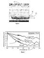
- Figure 5 shows a FIB microscopical photograph of the top surface 50 of a silicon-coated textured glass pane fabricated using a method embodying the present invention.
- the silicon film is of polycrystalline nature and has a thickness of about 1.5 ⁇ m (i.e., similar to the dimensions of the texture features). It was created by thermal annealing ("'solid-phase crystallisation") of a plasma enhanced chemical vapour deposition (PECVD)-deposited amorphous silicon film.
- PECVD plasma enhanced chemical vapour deposition
- the striking feature of the surface 50 of the silicon coated glass pane is its cauliflower-like nature, caused by the textured glass surface [note that the silicon film has a planar, smooth top surface if fabricated on a non-textured (i.e., planar) glass pane].
- the cauliflower-like top surface 50 of the silicon film is an indicator for good light trapping characteristics.
- Figure 6 shows a FIB microscopical photograph of a different region of the same sample, whereby additionally a trench was milled (using gallium ions) into the sample surface to reveal the cross-sectional properties of both the textured glass pane 52 and the polycrystalline silicon film 54 subsequently formed on the surface of the textured glass pane 52.
- the lateral marker 56 in Fig. 6 represents 2 ⁇ m. It can be seen that the poly-Si film 54 is everywhere in intimate contact with the surface of the textured glass pane 52 and that there are no voids or gaps between the glass pane 52 and the poly-Si film 54. This is advantageous for many device applications due to issues such as adhesion of the semiconductor film to the glass, long-term stability of the device, etc..
- the light trapping can be further improved in actual devices by incorporating a back-surface reflector (BSR) (not shown) for near-infrared photons.
- BSR back-surface reflector
- the BSR can, for instance, be a silver or aluminium film.
- the BSR is either deposited onto the semiconductor film (if the sunlight enters the semiconductor through the glass) or onto the non-textured glass surface (if the semiconductor-coated, textured side of the glass faces the sun).
- Figure 7 shows that excellent light trapping is realised in thin ( ⁇ 1.5 micron) polycrystalline silicon films formed on glass panes textured according to the described embodiment.
- the curve 70 labelled "Al-textured glass” was measured on the sample of Figure 5 .
- the plotted parameter is the measured internal absorption efficiency (IAE) which, for each wavelength, describes which fraction of those photons that entered the Si film is absorbed within the Si film. The higher the IAE the better the light trapping.
- IAE measured internal absorption efficiency
- glass panes textured in accordance with the described embodiment efficiently scatter light rays that pass through the glass panes, making them useful for other applications outside their use for photovoltaic devices.
- One such application is e.g. as glass panes for scattering windows or screens.
- the present invention is not limited to the dimensions and/or thin-film deposition techniques and/or reaction products removal techniques of the example embodiments described.
- the glass texturing processes were optimised for borosilicate glass, it will be appreciated that the processing can be chosen and optimised for different glasses, including sodalime glass, which is often used as a cheap window glass.
Landscapes
- Chemical & Material Sciences (AREA)
- Life Sciences & Earth Sciences (AREA)
- Materials Engineering (AREA)
- Chemical Kinetics & Catalysis (AREA)
- General Chemical & Material Sciences (AREA)
- Geochemistry & Mineralogy (AREA)
- Engineering & Computer Science (AREA)
- Organic Chemistry (AREA)
- Sustainable Development (AREA)
- Inorganic Chemistry (AREA)
- Surface Treatment Of Glass (AREA)
- Photovoltaic Devices (AREA)
- Formation Of Insulating Films (AREA)
- Joining Of Glass To Other Materials (AREA)
- Document Processing Apparatus (AREA)
Abstract
Description
- The present invention relates broadly to a method of texturing a glass surface, to a method of manufacturing a photovoltaic device, to a textured glass surface, and to a photovoltaic device.
- Textured glass surfaces are useful for a number of applications, including in photovoltaic devices or for applications in which it is desired to scatter light rays such that objects are no longer clearly visible through the glass.
- In photovoltaic devices, light trapping is used to trap light in the active region of the device. The more light is trapped in the device the higher the light-generated photocurrent, and consequently the higher the energy conversion efficiency of the device. Therefore, light trapping is an important issue when trying to improve the conversion efficiency of photovoltaic devices and is particularly important in thin-film devices. Because most photovoltaic devices involve a glass pane, light trapping in these devices can be realised by texturing the glass pane.
- Conventionally, chemical texturing or sand blasting are used for texturing glass panes. Alternative approaches have recently been disclosed for preparing textured glass surfaces. One of those approaches uses metal crystal deposits on a glass surface to form very fine crystals and thereby producing the glass texture effect. Another approach uses a liquid surface coating ("sol-gel") containing SiO2 spheres that, after densification, produces a textured glass surface.
- However, these methods have specific disadvantages for photovoltaic device applications. Both chemical texturing and sand blasting can cause cracks and non-uniform feature size on the glass surface, which can adversely affect photovoltaic device fabrication and/or performance (for instance by causing electrical shunts in the devices). On the other hand, the use of fine metal crystals for making a textured glass surface appears to be quite an expensive method. Finally, it appears to be difficult to scale up the sol-gel method to very large dimensions (∼ 1 m2) as required for photovoltaic panels.
- A need, therefore, exists to provide an alternative method of texturing a glass surface which addresses one or more of these disadvantages.
- In accordance with a first aspect of the present invention there is provided a method of texturing a glass surface, the method comprising the steps of coating the glass surface with a material film, stimulating a reaction at the interface between the glass and the material film resulting in the formation of reaction products at the interface, and removing the material film and the reaction products from the glass surface.
- In one embodiment, the step of stimulating the reaction at the interface comprises a thermal annealing process. The thermal annealing process may comprise a sequence of annealing steps at different temperatures. The thermal annealing process may be conducted in a controlled ambient atmosphere.
- The material film may comprise a single material or compound material. The glass surface may initially be substantially flat.
- The material film in one embodiment comprises aluminium. The reaction products may comprise aluminium oxide.
- The step of removing the material film and the reaction products may comprise one or more etching steps. The etching steps may comprise a chemical etch.
- The glass may comprise quartz, float glass, or non-float glass.
- In accordance with a second aspect of the present invention there is provided a method of manufacturing a photovoltaic device, the method comprises the steps of texturing a glass surface utilising the method as defined in the first aspect, and depositing a semiconductor film on the textured glass surface, whereby the glass-facing surface of the semiconductor film exhibits substantially the same degree of texture as the glass surface.
- In one embodiment, the semiconductor film is deposited in a manner such that substantially no gaps or voids exist between the textured glass surface and the semiconductor film.
- The method may further comprise forming a dielectric barrier layer between the glass surface and the semiconductor. The dielectric layer may be formed on the textured glass surface prior to the deposition of the semiconductor film. The dielectric barrier layer may comprise silicon oxide or silicon nitride.
- The semiconductor film may comprise a crystalline and/or an amorphous semiconductor material. The semiconductor material may comprise silicon.
- In accordance with a third aspect of the present invention there is provided a textured glass surface formed utilising the method as defined in the first aspect.
- In accordance with a fourth aspect of the present invention there is provided a photovoltaic device manufactured utilising the method as defined in the second aspect.
- In accordance with a fourth aspect of the present invention there is provided a photovoltaic device comprising a glass pane having a textured surface a semiconductor film formed on the textured surface of the glass pane and having an internal absorption efficiency greater than about 0.5 for photons in a wavelength range from about 600 to 1200 nm.
- Preferred embodiments of the invention will now be described, by way of example, with reference to the accompanying drawings in which:
-
Figures 1 to 4 are schematic drawings illustrating a method of texturing the surface of a glass pane, embodying the present invention. -
Figure 5 shows a FIB (focused ion beam) microscopical photograph of the top surface of a silicon-coated textured glass pane, embodying the present invention. -
Figure 6 shows a FIB microscopical photograph of a different region of the sample ofFigure 5 . -
Figure 7 shows the measured light trapping properties of the sample ofFigure 5 , compared with prior art samples. - The embodiments described provide methods of texturing a glass surface suitable for use in the manufacturing of thin-film semiconductor photovoltaic devices.
-
Figures 1 to 4 are schematic drawings illustrating a method of texturing the surface of aglass pane 10, embodying the present invention.Figure 1 shows theglass pane 10, having a substantially flat upper surface and being a borosilicate glass in an example embodiment. - In a first step shown in
Figure 2 , theglass pane 10 is coated with an aluminium film 11 utilising, in the example embodiment, thermal vacuum evaporation at about 10-5 Torr. In the example embodiment, the initial aluminium coating 11 is of a thickness of about 500 nm. - Next, the Al-coated glass pane is thermally annealed at elevated temperature, in the example embodiment in a two-step process with about 120 mins at about 500°C, followed by about 360 mins at about 620°C in a nitrogen atmosphere.
- In another embodiment, a three-step process with about 120 mins at about 500°C, followed by about 180 mins at about 560°C, followed by about 180 mins at about 630°C in a nitrogen atmosphere may be applied.
- It has been found by the applicants that the Al reacts spatially non-uniformly with the glass pane, forming reaction products in the form of mixtures (12 in
Figure 3 ) of aluminium oxide and silicon. A subsequent removal of both the Al film 11 and thereaction products 12 forms a textured glass surface as schematically shown inFigure 4 . In the example embodiment, a 2-step chemical etch with about 10 mins in 85% phosphoric acid solution at about 110°C, followed by about 20 to about 45 secs in a 1:1HF/HNO3 solution at room temperature was used to remove thereaction products 12 and aluminium film 11. - In another embodiment, a 2-step chemical etch with about 10 mins in phosphoric acid at about 110°C, followed by a second etch in a HF/HNO3 solution at room temperature where the HF/HNO3 is in the range from about 1:1 to 1:20 is applied. Depending on the ratio used, a short ultrasonic waterbath treatment may be utilised after the second etching step to completely remove all reaction products.
- It is noted here, that, depending on the type of removal technique, for example the type of etching solution, used, some amount of glass that has not reacted with the coating can also be removed, if desired.
- Dimples (13 in
Figure 4 ) in the glass pane result from the removal of the Al/glass reaction products 12. The average size of the dimples can be adjusted over a wide range (from less than 1 µm to up to 10 µm) by e.g. selecting a suitable thermal annealing profile and/or a suitable removal technique for the Al/glass reaction products 12. This dimple size is well suited for thin-film photovoltaic applications because in those devices the semiconductor film thickness is typically in the range 0.5 - 3 µm. - In the example embodiment, the method textures the glass in such a way that there are no "overhanging" regions, i.e. when the
textured glass pane 10 ofFig. 4 was illuminated by parallel light from above, there were no shaded regions within the dimples of the surface texture. This feature is advantageous for device applications, for instance if the subsequently formed semiconductor film needs to be in intimate contact with the glass everywhere (i.e., there must be no voids or gaps between the glass and the semiconductor film). - Another advantageous feature of textured glass samples embodying the present invention is that their transmission for light is only very weakly reduced by the texture.
-
Figure 5 shows a FIB microscopical photograph of thetop surface 50 of a silicon-coated textured glass pane fabricated using a method embodying the present invention. The silicon film is of polycrystalline nature and has a thickness of about 1.5 µm (i.e., similar to the dimensions of the texture features). It was created by thermal annealing ("'solid-phase crystallisation") of a plasma enhanced chemical vapour deposition (PECVD)-deposited amorphous silicon film. The striking feature of thesurface 50 of the silicon coated glass pane is its cauliflower-like nature, caused by the textured glass surface [note that the silicon film has a planar, smooth top surface if fabricated on a non-textured (i.e., planar) glass pane]. The cauliflower-liketop surface 50 of the silicon film is an indicator for good light trapping characteristics. -
Figure 6 shows a FIB microscopical photograph of a different region of the same sample, whereby additionally a trench was milled (using gallium ions) into the sample surface to reveal the cross-sectional properties of both thetextured glass pane 52 and thepolycrystalline silicon film 54 subsequently formed on the surface of thetextured glass pane 52. Thelateral marker 56 inFig. 6 represents 2 µm. It can be seen that the poly-Si film 54 is everywhere in intimate contact with the surface of thetextured glass pane 52 and that there are no voids or gaps between theglass pane 52 and the poly-Si film 54. This is advantageous for many device applications due to issues such as adhesion of the semiconductor film to the glass, long-term stability of the device, etc.. - Another feature visible in
Figure 6 , advantageous for good light trapping in thin-film photovoltaic devices, is the fact that in most regions of the sample the "top" and "bottom" surfaces 50 and 58 respectively of the poly-Si film 54 are sufficiently non-parallel, leading to the trapping of light due to the phenomenon of total internal reflection. However, it is noted that even if the twosurfaces surface 58 of the poly-Si film 54 is "directly transferred", resulting in a corresponding texture on thesurface 50 facing away from theglass 52, useful light trapping characteristics can still be achieved. - The light trapping can be further improved in actual devices by incorporating a back-surface reflector (BSR) (not shown) for near-infrared photons. The BSR can, for instance, be a silver or aluminium film. The BSR is either deposited onto the semiconductor film (if the sunlight enters the semiconductor through the glass) or onto the non-textured glass surface (if the semiconductor-coated, textured side of the glass faces the sun).
-
Figure 7 shows that excellent light trapping is realised in thin (∼1.5 micron) polycrystalline silicon films formed on glass panes textured according to the described embodiment. Thecurve 70 labelled "Al-textured glass" was measured on the sample ofFigure 5 . The plotted parameter is the measured internal absorption efficiency (IAE) which, for each wavelength, describes which fraction of those photons that entered the Si film is absorbed within the Si film. The higher the IAE the better the light trapping. - Also shown, for comparison, is the measured IAE of a 1.5-µm thick poly-Si film on a planar glass pane (curve 74) and on a sandblasted glass pane (curve 72). Clearly, the Al-textured glass provides by far the best light trapping of the three investigated structures. Note that the samples did not have a back surface reflector (BSR) during these optical measurements and hence the IAE of actual devices (such as thin-film photovoltaics) can be further improved by adding a suitable BSR.
- It is further noted that glass panes textured in accordance with the described embodiment efficiently scatter light rays that pass through the glass panes, making them useful for other applications outside their use for photovoltaic devices. One such application is e.g. as glass panes for scattering windows or screens.
- It will be appreciated by the person skilled in the art that numerous modifications and/or variations may be made to the present invention as shown in the specific embodiments without departing from the spirit or scope of the invention as broadly described. The present embodiments are, therefore, to be considered in all respects to be illustrative and not restrictive.
- For example, it will be appreciated that the present invention is not limited to the dimensions and/or thin-film deposition techniques and/or reaction products removal techniques of the example embodiments described.
- Furthermore, while in the embodiments described the glass texturing processes were optimised for borosilicate glass, it will be appreciated that the processing can be chosen and optimised for different glasses, including sodalime glass, which is often used as a cheap window glass.
Claims (16)
- A method of texturing a glass surface, the method comprising the steps of:- coating the glass surface with a material film,- stimulating a reaction at the interface between the glass and the material film resulting in the formation of reaction products at the interface, and- removing the material film and the reaction products from the glass surface.
- The method as claimed in claim 1, wherein the step of stimulating the reaction at the interface comprises a thermal annealing process.
- The method as claimed in claims 1 or 2, wherein the thermal annealing process comprises a sequence of annealing steps at different temperatures.
- The method as claimed in any one of the preceding claims, wherein the material film comprises a single material or compound material.
- The method as claimed in any one of the preceding claims, wherein the material film comprises aluminium.
- The method as claimed in claim 7, wherein the reaction products comprise aluminium oxide and/or silicon.
- The method as claimed in any one of the preceding claims, wherein the step of removing the material film and the reaction products comprises one or more etching steps.
- The method as claimed in any one of the preceding claims, wherein the glass comprises quartz, float glass, or non-float glass.
- A method of manufacturing a photovoltaic device, the method comprises the steps of texturing a glass surface utilising a method as claimed in any one of the preceding claims, and depositing a semiconductor film on the textured glass surface, whereby the glass-facing surface of the semiconductor film exhibits substantially the same degree of texture as the glass surface.
- The method as claimed in claim 9, wherein the method further comprises forming a dielectric barrier layer between the glass and the semiconductor.
- The method as claimed in claim 10, wherein the dielectric layer is formed on the textured glass surface prior to the deposition of the semiconductor film.
- The method as claimed in claim 10 or 11, wherein the barrier layer comprises silicon oxide or silicon nitride.
- The method as claimed in claim 12, wherein the semiconductor material comprises silicon.
- A textured glass surface formed utilising a method as claimed in claim 1.
- A photovoltaic device manufactured utilising a method as claimed in claim 9.
- A photovoltaic device comprising:- a glass pane having a textured surface;- a semiconductor film formed on the textured surface of the glass pane and having an internal absorption efficiency greater than about 0.5 for photons in a wavelength range from about 600 to 1200 nm.
Applications Claiming Priority (2)
| Application Number | Priority Date | Filing Date | Title |
|---|---|---|---|
| AU2003901559A AU2003901559A0 (en) | 2003-04-07 | 2003-04-07 | Glass texturing method |
| EP04721778A EP1613562B1 (en) | 2003-04-07 | 2004-03-19 | Glass texturing |
Related Parent Applications (1)
| Application Number | Title | Priority Date | Filing Date |
|---|---|---|---|
| EP04721778.1 Division | 2004-03-19 |
Publications (2)
| Publication Number | Publication Date |
|---|---|
| EP2295386A1 true EP2295386A1 (en) | 2011-03-16 |
| EP2295386B1 EP2295386B1 (en) | 2013-03-13 |
Family
ID=31500602
Family Applications (2)
| Application Number | Title | Priority Date | Filing Date |
|---|---|---|---|
| EP10186992A Expired - Lifetime EP2295386B1 (en) | 2003-04-07 | 2004-03-19 | Glass texturing |
| EP04721778A Expired - Lifetime EP1613562B1 (en) | 2003-04-07 | 2004-03-19 | Glass texturing |
Family Applications After (1)
| Application Number | Title | Priority Date | Filing Date |
|---|---|---|---|
| EP04721778A Expired - Lifetime EP1613562B1 (en) | 2003-04-07 | 2004-03-19 | Glass texturing |
Country Status (6)
| Country | Link |
|---|---|
| US (1) | US20060263606A1 (en) |
| EP (2) | EP2295386B1 (en) |
| CN (2) | CN1756723A (en) |
| AT (1) | ATE517068T1 (en) |
| AU (2) | AU2003901559A0 (en) |
| WO (1) | WO2004089841A1 (en) |
Families Citing this family (11)
| Publication number | Priority date | Publication date | Assignee | Title |
|---|---|---|---|---|
| TWI267897B (en) * | 2005-11-10 | 2006-12-01 | Tatung Co | Substrate with anti-reflection layer and its manufacturing method |
| US20070215195A1 (en) * | 2006-03-18 | 2007-09-20 | Benyamin Buller | Elongated photovoltaic cells in tubular casings |
| WO2010044269A1 (en) * | 2008-10-17 | 2010-04-22 | 株式会社アルバック | Manufacturing method for solar cell |
| EP2438140A1 (en) | 2009-06-04 | 2012-04-11 | Merck Patent GmbH | Two component etching |
| EP2319813B1 (en) * | 2009-10-26 | 2012-12-26 | Saint-Gobain Glass France | Structured glass pane and a photovoltaic module with such a glass pane |
| CN103493215A (en) * | 2010-09-03 | 2014-01-01 | 康宁股份有限公司 | Thin film silicon solar cell in multi-junction configuration on textured glass |
| CN104992990B (en) * | 2010-12-30 | 2018-05-11 | 深圳市石金科技股份有限公司 | A kind of method for reducing surface light reflectivity of silicon chip |
| JP6186377B2 (en) | 2012-12-18 | 2017-08-23 | パイオニア株式会社 | Light emitting device |
| NL2012010C2 (en) | 2013-12-20 | 2015-06-26 | Univ Delft Tech | A method for texturing a glass surface. |
| CN107689400B (en) * | 2016-07-29 | 2020-10-20 | 比亚迪股份有限公司 | Glass for solar cell and solar cell |
| CN111002115A (en) * | 2020-01-16 | 2020-04-14 | 程凯芬 | Anti-glare glass and processing method thereof |
Citations (2)
| Publication number | Priority date | Publication date | Assignee | Title |
|---|---|---|---|---|
| US3951633A (en) * | 1974-12-23 | 1976-04-20 | Combustion Engineering, Inc. | Method for producing patterned glass on a float ribbon |
| WO2000028602A1 (en) * | 1998-11-06 | 2000-05-18 | Pacific Solar Pty Limited | Thin films with light trapping |
Family Cites Families (8)
| Publication number | Priority date | Publication date | Assignee | Title |
|---|---|---|---|---|
| JPS5123266B2 (en) * | 1972-04-21 | 1976-07-15 | ||
| US4042449A (en) * | 1975-07-24 | 1977-08-16 | The United States Of America As Represented By The Secretary Of The Navy | Method of making a reticle-lens |
| DE3523960A1 (en) * | 1985-07-04 | 1987-01-08 | Licentia Gmbh | METHOD FOR METALLIZING AN ELECTRICALLY BAD CONDUCTING SUBSTRATE FROM AN INORGANIC MATERIAL |
| US4794048A (en) * | 1987-05-04 | 1988-12-27 | Allied-Signal Inc. | Ceramic coated metal substrates for electronic applications |
| DE4125200A1 (en) * | 1991-07-30 | 1993-02-04 | Siemens Ag | METHOD FOR PRODUCING A LUMINAIRE LAYER ON A SUBSTRATE |
| DE4230732C1 (en) * | 1992-09-14 | 1993-09-09 | Schott Glaswerke, 55122 Mainz, De | |
| DE4318178C2 (en) * | 1993-06-01 | 1995-07-13 | Schott Glaswerke | Process for the chemical removal of coatings connected to the surface of a substrate made of glass, glass ceramic or ceramic, substrate produced in this way and process for producing a new decoration on this substrate |
| JP4465429B2 (en) * | 2002-02-21 | 2010-05-19 | 株式会社リコー | Laser processing method |
-
2003
- 2003-04-07 AU AU2003901559A patent/AU2003901559A0/en not_active Abandoned
-
2004
- 2004-03-19 EP EP10186992A patent/EP2295386B1/en not_active Expired - Lifetime
- 2004-03-19 US US10/553,030 patent/US20060263606A1/en not_active Abandoned
- 2004-03-19 CN CNA2004800058806A patent/CN1756723A/en active Pending
- 2004-03-19 WO PCT/AU2004/000339 patent/WO2004089841A1/en not_active Ceased
- 2004-03-19 AU AU2004228064A patent/AU2004228064B2/en not_active Ceased
- 2004-03-19 EP EP04721778A patent/EP1613562B1/en not_active Expired - Lifetime
- 2004-03-19 AT AT04721778T patent/ATE517068T1/en not_active IP Right Cessation
- 2004-03-19 CN CN2009101607966A patent/CN101624266B/en not_active Expired - Fee Related
Patent Citations (2)
| Publication number | Priority date | Publication date | Assignee | Title |
|---|---|---|---|---|
| US3951633A (en) * | 1974-12-23 | 1976-04-20 | Combustion Engineering, Inc. | Method for producing patterned glass on a float ribbon |
| WO2000028602A1 (en) * | 1998-11-06 | 2000-05-18 | Pacific Solar Pty Limited | Thin films with light trapping |
Non-Patent Citations (3)
| Title |
|---|
| WIDENBORG P ET AL: "Back electrode formation for poly-Si thin film solar cells on glass having AIC-grown seeding layer", SOLAR ENERGY MATERIALS AND SOLAR CELLS, ELSEVIER SCIENCE PUBLISHERS, AMSTERDAM, NL, vol. 74, no. 1-4, 1 October 2002 (2002-10-01), pages 305 - 314, XP004376956, ISSN: 0927-0248 * |
| WIDENBORG P I ET AL: "Surface morphology of poly-Si films made by aluminium-induced crystallisation on glass substrates", JOURNAL OF CRYSTAL GROWTH, ELSEVIER, AMSTERDAM, NL, vol. 242, no. 3-4, 1 July 2002 (2002-07-01), pages 270 - 282, XP004368857, ISSN: 0022-0248 * |
| WIDENBORG P I ET AL: "Thick poly-Si films fabricated by the aluminium-induced crystallization bi-layer process on glass substrates", CONFERENCE RECORD OF THE 29TH IEEE PHOTOVOLTAIC SPECIALISTS CONFERENCE 20020519; 20020519 - 20020524 NEW YORK, NY : IEEE, US, vol. CONF. 29, 19 May 2002 (2002-05-19), pages 1206 - 1209, XP010666498, ISBN: 978-0-7803-7471-3 * |
Also Published As
| Publication number | Publication date |
|---|---|
| US20060263606A1 (en) | 2006-11-23 |
| CN101624266B (en) | 2011-05-11 |
| AU2004228064A1 (en) | 2004-10-21 |
| CN101624266A (en) | 2010-01-13 |
| CN1756723A (en) | 2006-04-05 |
| EP1613562B1 (en) | 2011-07-20 |
| ATE517068T1 (en) | 2011-08-15 |
| AU2003901559A0 (en) | 2003-05-01 |
| WO2004089841A1 (en) | 2004-10-21 |
| EP1613562A4 (en) | 2008-10-01 |
| AU2004228064B2 (en) | 2008-12-04 |
| EP2295386B1 (en) | 2013-03-13 |
| EP1613562A1 (en) | 2006-01-11 |
Similar Documents
| Publication | Publication Date | Title |
|---|---|---|
| US6420647B1 (en) | Texturing of glass by SiO2 film | |
| AU2024287247A1 (en) | Solar cell, manufacturing method thereof, and photovoltaic module | |
| EP1918999B1 (en) | Method for producing single crystal silicon solar cell and single crystal silicon solar cell | |
| CN102361833B (en) | The method of transparent glass substrate and this substrate of manufacture | |
| US8076215B2 (en) | Method of forming an electronic device using a separation technique | |
| EP2295386B1 (en) | Glass texturing | |
| PT914486E (en) | COATING SUBSTRATE | |
| CN101748405B (en) | Transparent conducting film and preparation method thereof, solar battery and flat panel display device | |
| JP5841074B2 (en) | Glass substrate coated with a layer of improved mechanical strength | |
| JP2012195620A (en) | Method for manufacturing photoelectric conversion device and photoelectric conversion device | |
| US7517552B2 (en) | Glass beads coating process | |
| JP2005500702A5 (en) | ||
| CN103781738A (en) | Photocatalytic material and window glass or photovoltaic cell comprising the material | |
| Park et al. | Method for fabricating textured high-haze ZnO: Al transparent conduction oxide films on chemically etched glass substrates | |
| US20120148814A1 (en) | Transparent glass body, method for the production thereof, and use thereof | |
| EP3008152B1 (en) | Chemical composition for semiconductor manufacturing processes | |
| TW201332136A (en) | By leaching to form a diffusion barrier layer of the photovoltaic device | |
| CN103474504B (en) | A method for preparing reflective film, solar cell panel and crystalline silicon wafer thereof | |
| JP2012244029A (en) | Thin film solar cell substrate and manufacturing method thereof and thin film solar cell | |
| WO2025042702A1 (en) | Article with a substrate and multilayer coating on the substrate and solar panel incorporating the article | |
| KR20150002517A (en) | Transparent substrate having an anti-reflective multilayered coating thereon and method for preparing the same | |
| KR20150002516A (en) | Transparent substrate having an anti-reflective multilayered coating thereon and method for preparing the same | |
| EP2515340A2 (en) | ZnO-based thin film for photovoltaic cell and method of its manufacturing on a substrate |
Legal Events
| Date | Code | Title | Description |
|---|---|---|---|
| PUAI | Public reference made under article 153(3) epc to a published international application that has entered the european phase |
Free format text: ORIGINAL CODE: 0009012 |
|
| AC | Divisional application: reference to earlier application |
Ref document number: 1613562 Country of ref document: EP Kind code of ref document: P |
|
| AK | Designated contracting states |
Kind code of ref document: A1 Designated state(s): AT BE BG CH CY CZ DE DK EE ES FI FR GB GR HU IE IT LI LU MC NL PL PT RO SE SI SK TR |
|
| 17P | Request for examination filed |
Effective date: 20110914 |
|
| REG | Reference to a national code |
Ref country code: DE Ref legal event code: R079 Ref document number: 602004041380 Country of ref document: DE Free format text: PREVIOUS MAIN CLASS: C03C0015000000 Ipc: C03C0017090000 |
|
| RIC1 | Information provided on ipc code assigned before grant |
Ipc: C03C 17/34 20060101ALI20120810BHEP Ipc: C03C 17/36 20060101ALI20120810BHEP Ipc: C03C 17/09 20060101AFI20120810BHEP |
|
| GRAP | Despatch of communication of intention to grant a patent |
Free format text: ORIGINAL CODE: EPIDOSNIGR1 |
|
| GRAS | Grant fee paid |
Free format text: ORIGINAL CODE: EPIDOSNIGR3 |
|
| GRAA | (expected) grant |
Free format text: ORIGINAL CODE: 0009210 |
|
| AC | Divisional application: reference to earlier application |
Ref document number: 1613562 Country of ref document: EP Kind code of ref document: P |
|
| AK | Designated contracting states |
Kind code of ref document: B1 Designated state(s): AT BE BG CH CY CZ DE DK EE ES FI FR GB GR HU IE IT LI LU MC NL PL PT RO SE SI SK TR |
|
| REG | Reference to a national code |
Ref country code: GB Ref legal event code: FG4D |
|
| REG | Reference to a national code |
Ref country code: AT Ref legal event code: REF Ref document number: 600704 Country of ref document: AT Kind code of ref document: T Effective date: 20130315 Ref country code: CH Ref legal event code: EP |
|
| REG | Reference to a national code |
Ref country code: IE Ref legal event code: FG4D |
|
| REG | Reference to a national code |
Ref country code: DE Ref legal event code: R096 Ref document number: 602004041380 Country of ref document: DE Effective date: 20130508 |
|
| PG25 | Lapsed in a contracting state [announced via postgrant information from national office to epo] |
Ref country code: SE Free format text: LAPSE BECAUSE OF FAILURE TO SUBMIT A TRANSLATION OF THE DESCRIPTION OR TO PAY THE FEE WITHIN THE PRESCRIBED TIME-LIMIT Effective date: 20130313 Ref country code: BG Free format text: LAPSE BECAUSE OF FAILURE TO SUBMIT A TRANSLATION OF THE DESCRIPTION OR TO PAY THE FEE WITHIN THE PRESCRIBED TIME-LIMIT Effective date: 20130613 Ref country code: ES Free format text: LAPSE BECAUSE OF FAILURE TO SUBMIT A TRANSLATION OF THE DESCRIPTION OR TO PAY THE FEE WITHIN THE PRESCRIBED TIME-LIMIT Effective date: 20130624 |
|
| PGFP | Annual fee paid to national office [announced via postgrant information from national office to epo] |
Ref country code: DE Payment date: 20130514 Year of fee payment: 10 |
|
| REG | Reference to a national code |
Ref country code: AT Ref legal event code: MK05 Ref document number: 600704 Country of ref document: AT Kind code of ref document: T Effective date: 20130313 |
|
| REG | Reference to a national code |
Ref country code: NL Ref legal event code: VDEP Effective date: 20130313 |
|
| PG25 | Lapsed in a contracting state [announced via postgrant information from national office to epo] |
Ref country code: FI Free format text: LAPSE BECAUSE OF FAILURE TO SUBMIT A TRANSLATION OF THE DESCRIPTION OR TO PAY THE FEE WITHIN THE PRESCRIBED TIME-LIMIT Effective date: 20130313 Ref country code: SI Free format text: LAPSE BECAUSE OF FAILURE TO SUBMIT A TRANSLATION OF THE DESCRIPTION OR TO PAY THE FEE WITHIN THE PRESCRIBED TIME-LIMIT Effective date: 20130313 Ref country code: GR Free format text: LAPSE BECAUSE OF FAILURE TO SUBMIT A TRANSLATION OF THE DESCRIPTION OR TO PAY THE FEE WITHIN THE PRESCRIBED TIME-LIMIT Effective date: 20130614 |
|
| PGFP | Annual fee paid to national office [announced via postgrant information from national office to epo] |
Ref country code: FR Payment date: 20130612 Year of fee payment: 10 |
|
| PG25 | Lapsed in a contracting state [announced via postgrant information from national office to epo] |
Ref country code: BE Free format text: LAPSE BECAUSE OF FAILURE TO SUBMIT A TRANSLATION OF THE DESCRIPTION OR TO PAY THE FEE WITHIN THE PRESCRIBED TIME-LIMIT Effective date: 20130313 |
|
| PG25 | Lapsed in a contracting state [announced via postgrant information from national office to epo] |
Ref country code: EE Free format text: LAPSE BECAUSE OF FAILURE TO SUBMIT A TRANSLATION OF THE DESCRIPTION OR TO PAY THE FEE WITHIN THE PRESCRIBED TIME-LIMIT Effective date: 20130313 Ref country code: PT Free format text: LAPSE BECAUSE OF FAILURE TO SUBMIT A TRANSLATION OF THE DESCRIPTION OR TO PAY THE FEE WITHIN THE PRESCRIBED TIME-LIMIT Effective date: 20130715 Ref country code: MC Free format text: LAPSE BECAUSE OF NON-PAYMENT OF DUE FEES Effective date: 20130331 Ref country code: AT Free format text: LAPSE BECAUSE OF FAILURE TO SUBMIT A TRANSLATION OF THE DESCRIPTION OR TO PAY THE FEE WITHIN THE PRESCRIBED TIME-LIMIT Effective date: 20130313 Ref country code: SK Free format text: LAPSE BECAUSE OF FAILURE TO SUBMIT A TRANSLATION OF THE DESCRIPTION OR TO PAY THE FEE WITHIN THE PRESCRIBED TIME-LIMIT Effective date: 20130313 Ref country code: CZ Free format text: LAPSE BECAUSE OF FAILURE TO SUBMIT A TRANSLATION OF THE DESCRIPTION OR TO PAY THE FEE WITHIN THE PRESCRIBED TIME-LIMIT Effective date: 20130313 Ref country code: RO Free format text: LAPSE BECAUSE OF FAILURE TO SUBMIT A TRANSLATION OF THE DESCRIPTION OR TO PAY THE FEE WITHIN THE PRESCRIBED TIME-LIMIT Effective date: 20130313 Ref country code: NL Free format text: LAPSE BECAUSE OF FAILURE TO SUBMIT A TRANSLATION OF THE DESCRIPTION OR TO PAY THE FEE WITHIN THE PRESCRIBED TIME-LIMIT Effective date: 20130313 |
|
| REG | Reference to a national code |
Ref country code: CH Ref legal event code: PL |
|
| PG25 | Lapsed in a contracting state [announced via postgrant information from national office to epo] |
Ref country code: PL Free format text: LAPSE BECAUSE OF FAILURE TO SUBMIT A TRANSLATION OF THE DESCRIPTION OR TO PAY THE FEE WITHIN THE PRESCRIBED TIME-LIMIT Effective date: 20130313 |
|
| REG | Reference to a national code |
Ref country code: IE Ref legal event code: MM4A |
|
| PLBE | No opposition filed within time limit |
Free format text: ORIGINAL CODE: 0009261 |
|
| STAA | Information on the status of an ep patent application or granted ep patent |
Free format text: STATUS: NO OPPOSITION FILED WITHIN TIME LIMIT |
|
| PG25 | Lapsed in a contracting state [announced via postgrant information from national office to epo] |
Ref country code: IE Free format text: LAPSE BECAUSE OF NON-PAYMENT OF DUE FEES Effective date: 20130319 Ref country code: LI Free format text: LAPSE BECAUSE OF NON-PAYMENT OF DUE FEES Effective date: 20130331 Ref country code: CH Free format text: LAPSE BECAUSE OF NON-PAYMENT OF DUE FEES Effective date: 20130331 Ref country code: DK Free format text: LAPSE BECAUSE OF FAILURE TO SUBMIT A TRANSLATION OF THE DESCRIPTION OR TO PAY THE FEE WITHIN THE PRESCRIBED TIME-LIMIT Effective date: 20130313 |
|
| 26N | No opposition filed |
Effective date: 20131216 |
|
| GBPC | Gb: european patent ceased through non-payment of renewal fee |
Effective date: 20130613 |
|
| PG25 | Lapsed in a contracting state [announced via postgrant information from national office to epo] |
Ref country code: IT Free format text: LAPSE BECAUSE OF FAILURE TO SUBMIT A TRANSLATION OF THE DESCRIPTION OR TO PAY THE FEE WITHIN THE PRESCRIBED TIME-LIMIT Effective date: 20130313 |
|
| REG | Reference to a national code |
Ref country code: DE Ref legal event code: R097 Ref document number: 602004041380 Country of ref document: DE Effective date: 20131216 |
|
| PG25 | Lapsed in a contracting state [announced via postgrant information from national office to epo] |
Ref country code: GB Free format text: LAPSE BECAUSE OF NON-PAYMENT OF DUE FEES Effective date: 20130613 |
|
| REG | Reference to a national code |
Ref country code: DE Ref legal event code: R119 Ref document number: 602004041380 Country of ref document: DE |
|
| REG | Reference to a national code |
Ref country code: FR Ref legal event code: ST Effective date: 20141128 |
|
| REG | Reference to a national code |
Ref country code: DE Ref legal event code: R119 Ref document number: 602004041380 Country of ref document: DE Effective date: 20141001 |
|
| PG25 | Lapsed in a contracting state [announced via postgrant information from national office to epo] |
Ref country code: DE Free format text: LAPSE BECAUSE OF NON-PAYMENT OF DUE FEES Effective date: 20141001 Ref country code: FR Free format text: LAPSE BECAUSE OF NON-PAYMENT OF DUE FEES Effective date: 20140331 |
|
| PG25 | Lapsed in a contracting state [announced via postgrant information from national office to epo] |
Ref country code: CY Free format text: LAPSE BECAUSE OF FAILURE TO SUBMIT A TRANSLATION OF THE DESCRIPTION OR TO PAY THE FEE WITHIN THE PRESCRIBED TIME-LIMIT Effective date: 20130313 Ref country code: TR Free format text: LAPSE BECAUSE OF FAILURE TO SUBMIT A TRANSLATION OF THE DESCRIPTION OR TO PAY THE FEE WITHIN THE PRESCRIBED TIME-LIMIT Effective date: 20130313 |
|
| PG25 | Lapsed in a contracting state [announced via postgrant information from national office to epo] |
Ref country code: LU Free format text: LAPSE BECAUSE OF NON-PAYMENT OF DUE FEES Effective date: 20130319 Ref country code: HU Free format text: LAPSE BECAUSE OF FAILURE TO SUBMIT A TRANSLATION OF THE DESCRIPTION OR TO PAY THE FEE WITHIN THE PRESCRIBED TIME-LIMIT; INVALID AB INITIO Effective date: 20040319 |