EP2293393B1 - Electric connector - Google Patents
Electric connector Download PDFInfo
- Publication number
- EP2293393B1 EP2293393B1 EP09758058.3A EP09758058A EP2293393B1 EP 2293393 B1 EP2293393 B1 EP 2293393B1 EP 09758058 A EP09758058 A EP 09758058A EP 2293393 B1 EP2293393 B1 EP 2293393B1
- Authority
- EP
- European Patent Office
- Prior art keywords
- housing
- conductive member
- contacts
- lead
- contact
- Prior art date
- Legal status (The legal status is an assumption and is not a legal conclusion. Google has not performed a legal analysis and makes no representation as to the accuracy of the status listed.)
- Active
Links
Images


Classifications
-
- H—ELECTRICITY
- H01—ELECTRIC ELEMENTS
- H01R—ELECTRICALLY-CONDUCTIVE CONNECTIONS; STRUCTURAL ASSOCIATIONS OF A PLURALITY OF MUTUALLY-INSULATED ELECTRICAL CONNECTING ELEMENTS; COUPLING DEVICES; CURRENT COLLECTORS
- H01R13/00—Details of coupling devices of the kinds covered by groups H01R12/70 or H01R24/00 - H01R33/00
- H01R13/646—Details of coupling devices of the kinds covered by groups H01R12/70 or H01R24/00 - H01R33/00 specially adapted for high-frequency, e.g. structures providing an impedance match or phase match
- H01R13/6461—Means for preventing cross-talk
- H01R13/6471—Means for preventing cross-talk by special arrangement of ground and signal conductors, e.g. GSGS [Ground-Signal-Ground-Signal]
-
- H—ELECTRICITY
- H01—ELECTRIC ELEMENTS
- H01R—ELECTRICALLY-CONDUCTIVE CONNECTIONS; STRUCTURAL ASSOCIATIONS OF A PLURALITY OF MUTUALLY-INSULATED ELECTRICAL CONNECTING ELEMENTS; COUPLING DEVICES; CURRENT COLLECTORS
- H01R13/00—Details of coupling devices of the kinds covered by groups H01R12/70 or H01R24/00 - H01R33/00
- H01R13/648—Protective earth or shield arrangements on coupling devices, e.g. anti-static shielding
- H01R13/658—High frequency shielding arrangements, e.g. against EMI [Electro-Magnetic Interference] or EMP [Electro-Magnetic Pulse]
- H01R13/6581—Shield structure
- H01R13/6582—Shield structure with resilient means for engaging mating connector
- H01R13/6583—Shield structure with resilient means for engaging mating connector with separate conductive resilient members between mating shield members
-
- H—ELECTRICITY
- H01—ELECTRIC ELEMENTS
- H01R—ELECTRICALLY-CONDUCTIVE CONNECTIONS; STRUCTURAL ASSOCIATIONS OF A PLURALITY OF MUTUALLY-INSULATED ELECTRICAL CONNECTING ELEMENTS; COUPLING DEVICES; CURRENT COLLECTORS
- H01R13/00—Details of coupling devices of the kinds covered by groups H01R12/70 or H01R24/00 - H01R33/00
- H01R13/648—Protective earth or shield arrangements on coupling devices, e.g. anti-static shielding
- H01R13/658—High frequency shielding arrangements, e.g. against EMI [Electro-Magnetic Interference] or EMP [Electro-Magnetic Pulse]
- H01R13/6581—Shield structure
- H01R13/6585—Shielding material individually surrounding or interposed between mutually spaced contacts
- H01R13/6589—Shielding material individually surrounding or interposed between mutually spaced contacts with wires separated by conductive housing parts
-
- H—ELECTRICITY
- H01—ELECTRIC ELEMENTS
- H01R—ELECTRICALLY-CONDUCTIVE CONNECTIONS; STRUCTURAL ASSOCIATIONS OF A PLURALITY OF MUTUALLY-INSULATED ELECTRICAL CONNECTING ELEMENTS; COUPLING DEVICES; CURRENT COLLECTORS
- H01R13/00—Details of coupling devices of the kinds covered by groups H01R12/70 or H01R24/00 - H01R33/00
- H01R13/648—Protective earth or shield arrangements on coupling devices, e.g. anti-static shielding
- H01R13/658—High frequency shielding arrangements, e.g. against EMI [Electro-Magnetic Interference] or EMP [Electro-Magnetic Pulse]
- H01R13/6591—Specific features or arrangements of connection of shield to conductive members
- H01R13/6592—Specific features or arrangements of connection of shield to conductive members the conductive member being a shielded cable
- H01R13/6593—Specific features or arrangements of connection of shield to conductive members the conductive member being a shielded cable the shield being composed of different pieces
-
- H—ELECTRICITY
- H01—ELECTRIC ELEMENTS
- H01R—ELECTRICALLY-CONDUCTIVE CONNECTIONS; STRUCTURAL ASSOCIATIONS OF A PLURALITY OF MUTUALLY-INSULATED ELECTRICAL CONNECTING ELEMENTS; COUPLING DEVICES; CURRENT COLLECTORS
- H01R13/00—Details of coupling devices of the kinds covered by groups H01R12/70 or H01R24/00 - H01R33/00
- H01R13/648—Protective earth or shield arrangements on coupling devices, e.g. anti-static shielding
- H01R13/658—High frequency shielding arrangements, e.g. against EMI [Electro-Magnetic Interference] or EMP [Electro-Magnetic Pulse]
- H01R13/6591—Specific features or arrangements of connection of shield to conductive members
- H01R13/6597—Specific features or arrangements of connection of shield to conductive members the conductive member being a contact of the connector
-
- H—ELECTRICITY
- H01—ELECTRIC ELEMENTS
- H01R—ELECTRICALLY-CONDUCTIVE CONNECTIONS; STRUCTURAL ASSOCIATIONS OF A PLURALITY OF MUTUALLY-INSULATED ELECTRICAL CONNECTING ELEMENTS; COUPLING DEVICES; CURRENT COLLECTORS
- H01R13/00—Details of coupling devices of the kinds covered by groups H01R12/70 or H01R24/00 - H01R33/00
- H01R13/66—Structural association with built-in electrical component
- H01R13/665—Structural association with built-in electrical component with built-in electronic circuit
- H01R13/6658—Structural association with built-in electrical component with built-in electronic circuit on printed circuit board
Description
- The present invention relates to electrical connectors having a plurality of first and second contacts.
- A conventional electrical connector of this type has a housing, a plurality of first and second contacts that are arranged on opposite sides in a thickness direction of the housing, and a metal plate interposed between the first and second contacts, the metal plate being connected to ground to reduce crosstalk induced between the first and second contacts (see, e.g., Patent Literature 1).
- Patent Literature 1 Japanese Unexamined Patent Publication No.
2005-327701 - United States Published Patent Application No.
US 2002/0028604 A1 discloses in Figures 59 and 61a a connector comprising a housing which defines a receiving opening, and has two groups of contacts arranged in rows along opposite sides of the receiving opening. A shielding member is positioned within the receiving opening between the two groups of contacts. The shielding member is connected to ground by means of a second shielding member extending from a plug which is inserted into the receiving opening. - United States Published Patent Application No.
US 2003/0236031 A1 discloses a high-speed high-density intercoupling component (connector) for receiving an array of contacts within a digital or analog transmission system having an electrical ground circuit and a chassis ground circuit. The connector comprises a segment formed of electrically insulative material, the segment including a plurality of holes disposed on its upper surface and arranged in a predetermined footprint and one or more shield members formed of electrically conductive material disposed within the segment for connecting to the chassis ground circuit. The connector may include an array of electrically conductive contacts within the plurality of holes disposed on the segment. One or more of these contacts may be configured to electrically connect with the electrical ground circuit. - United States Published Patent Application No.
US2002/0028604 A1 discloses a shielded telecommunications connector comprising a conductive core having core side walls and a horizontal shield joined to and perpendicular to the side walls. - In the electrical connector, however, a portion of the metal plate is exposed along the lateral surfaces of the housing so as to contact a metal shell covering the outer periphery of the housing, which metal shell is connected to a ground conductor of a cable coupled to the electrical connector, or to a ground circuit on a printed board to which the electrical connector is mounted.
- That is, the electrical connector has a structure that definitely requires extraction of a portion of the metal plate out of the housing; therefore, the housing needs to be constructed in a two-piece structure, or extraction holes need to be provided in the housing. Thus, the electrical connector has a disadvantage that the structure thereof inevitably has a complicated structure.
- The present invention was made against the backdrop of the foregoing circumstances, and an object of the invention is to provide a novel electrical connector in which a crosstalk prevention member such as a metal plate can be readily connected to a ground without making the structure of the connector itself complicated.
- An electrical connector according to the present invention is defined in claim 1
- In such an electrical connector, ground connection is established with the conductive member simply by inserting the conductive member into the receiving hole in the housing so that the conductive member contacts a ground contact of at least one of the first and second contact groups. Accordingly, it is possible to ground the conductive member without providing the housing as a two-piece structure and without boring guiding holes in the housing as in the conventional example, so that the electrical connector can be simplified in structure. In addition, most suitable ground connection is given to the present electrical connector by changing the positions and/or number of the ground contact. Further, as the conductive member is interposed between the first and second contact groups so as to contact the ground contact, crosstalk is less likely to occur between signaling contacts of the first contact group and signaling contacts of the second contact group. Moreover, as at least one of the first and second contact groups includes a ground contact disposed between the signaling contacts of that contact group, crosstalk is less likely to occur among the signaling contacts of that contact group.
- The conductive member preferably includes a grounding portion in the form of a projection that is in contact with the ground contact. In this aspect of the invention, the grounding portion contacts the ground contact with the conductive member received in the receiving hole of the housing. Thus, the conductive member can be readily brought into contact with the ground contact while maintaining its function as a conductive member to reduce crosstalk between the signaling contacts of the first contact group and the signaling contacts of the second contact group.
- If the conductive member is a metal plate, the grounding portion may be a cut-and-raised piece formed by cutting and bending a portion of the conductive member. In this aspect of the invention, the conductive member and the grounding portion may be fabricated easily by simply cutting and raising a portion of the metal plate using press forming or some other process.
- If the conductive member is a plate-like non-conductive material with peripheral surfaces thereof coated with metal, the grounding portion may be a projection provided on the non-conductive material and coated with metal. In this aspect of the invention, the conductive member and the grounding portion can be easily fabricated only by providing a projection on a non-conductive material of resin or other material, and by coating the non-conductive material and the projection with metal.
- First locking means for locking the conductive member received in the receiving hole of the housing is preferably provided on at least one of an inner surface of the receiving hole in the housing and the conductive member. In this aspect of the invention, the first locking means locks the conductive member as received in the receiving hole in the housing, the conductive member is readily positioned in relation to the receiving hole in the housing and is prevented from slipping out of the receiving hole.
- The conductive member may include: a first crosstalk reducer constituted by said leading end portion; and a second crosstalk reducer on a rear end side thereof, being interposed between rear end portions of the signaling contacts of the first contact group and rear end portions of the signaling contacts of the second contact group.
- In this aspect of the invention, the first crosstalk reducer interposed between the middle portions of the signaling contacts of the first contact group and the middle portions of the signaling contacts of the second contact group helps to reduce crosstalk between the sets of the middle portions. Also, the second crosstalk reducer interposed between the rear end portions of the signaling contacts of the first contact group and the rear end portions of the signaling contacts of the second contact group helps to reduce crosstalk between the sets of the rear end portions. Accordingly, variation in transmission characteristics is reduced among the contacts, so that an electrical connector of high performance can be provided.
- If the electrical connector is connectable with a plurality of lead wires, the electrical connector may further includes a lead connection assisting member removably provided at a rear end of the housing. In this case, the signaling contacts of the first and second contact groups may have the middle portions arranged on the opposite sides of the receiving hole in the housing and also have the rear end portions projecting out of a rear surface of the housing. The lead connection assisting member may include: first and second support tables for providing support in soldering the rear end portions of the signaling contacts of the first and second contact groups to cores taken from leading ends of the lead wires; and first lead insertion grooves and second lead insertion grooves provided on rear end sides of the first support table and second support table, respectively, the first and second lead insertion grooves being arranged at equal pitch distance to the pitch distance of the signaling contacts of the first and second contact groups, the first and second lead insertion grooves being adapted to receive and temporarily hold the respective leading ends of the lead wires. The first crosstalk reducer is received in the receiving hole in the housing, and the second crosstalk reducer is interposed between a portion of the lead connection assisting member including the first support table and the first lead insertion grooves and a portion of the lead connection assisting member including the second support table and the second lead insertion grooves of the lead connection assisting member.
- In this aspect of the invention, as the second crosstalk reducer of the conductive member is interposed between the first support table as well as the first lead insertion grooves and the second support table as well as the second lead insertion grooves, it is possible to reduce crosstalk that may occur between the rear end portions of the signaling contacts of the first contact group as well as the cores of the lead wires connected thereto and the rear end portions of the signaling contacts of the second contact group as well as the cores of the lead wires connected thereto. Further, the first and second lead insertion grooves of the lead connection assisting member serves temporarily hold the leading ends of the lead wires on the rear side of the housing. In addition, the cores taken from the leading ends of the lead wires, together with the rear end portions of the signaling contacts of the first and second contact groups projecting out of the rear surface of the housing, are supported on the support tables of the lead connection assisting member. Thus, the cores and the rear end portions of the contacts can be soldered to one another in a single collective soldering using a pulse heating or other method, and also the solder can be supplied in an even amount to each soldered portion. Accordingly, it becomes possible to improve the mass productivity of the electrical connector and to reduce variation in transmission characteristics among the lead wires due to an uneven supply amount of solder to the soldered portions. It is thus possible to provide electrical connectors of high performance.
- A pair of guide means for movably guiding the lead connection assisting member in a longitudinal direction may preferably be provided on opposite ends of the rear end of the housing. In this aspect of the invention, the lead connection assisting member is guided by the pair of guide means and attached to the rear end of the housing, facilitating attachment of the lead connection assisting member to the housing. It is thus possible to reduce assembly costs.
- Second locking means is preferably provided on at least one of the pair of guide means and the lead connection assisting member, the second locking means being adapted to lock the lead connection assisting member as guided by the guide means and as attached to the rear end of the housing. In this aspect of the invention, the second locking means locks the lead connection assisting member as guided by the guide means and as attached to the rear end of the housing. In this manner, the lead connection assisting member is readily attached to the rear end of the housing, and further assembly cost can be reduced. Moreover, it is possible to prevent the lead connection assisting member from slipping off from the rear end of the housing.
- First guide grooves and second guide grooves may preferably be provided in the first and second support tables, respectively, of the lead connection assisting member in such a manner as to communicate with the first and second lead insertion grooves, the first and second guide grooves being adapted to guide the rear end portions of the signaling contacts of the first and second contact groups, respectively. In this aspect of the invention, upon attachment of the lead connection assisting member on the rear of the housing, the rear end portions of the signaling contacts of the first and second contact groups enter the first and second guide grooves on the support tables to be thereby guided and positioned in places so as to be opposed to the first and second lead insertion grooves. In this manner, the rear end portions of the contacts are readily aligned in relation to the cores of the lead wires located and held in the first and second lead insertion grooves. It is thus possible to further reduce assembly costs.
- The first and second lead insertion grooves may each have a slightly smaller lateral dimension than each lateral dimension of the leading ends of the lead wires such that the leading ends of the lead wires are allowed to be press-fitted and retained in the first and second lead insertion grooves. First and second lead insertion grooves may each have barbs pointing inward at opposite ends of an open side thereof, the barbs preventing the leading ends of the lead wires from slipping off. In these aspects of the invention, the leading ends of the lead wires are reliably positioned and retained, improving accuracy in soldering.
- The above electrical connector may include a shield cover for covering peripheral surfaces of the housing and a case for protecting an entire proximal end of the electrical connector.
- If the cores are soldered to the rear end portions of the signaling contacts, the above electrical connector may further include a block of insulating resin, the block being embedded with the rear end portions of the signaling contacts, the rear end of the ground contact, the leading ends of the lead wires with the cores thereof soldered to the rear end portions of the signaling contacts, and the multilayer circuit board excluding a leading end thereof.
- The block can retain the soldered state of the cores of the lead wires with the signaling conductors or with the rear end portions of the signaling contacts, so that it is possible to prevent the soldering from inadvertently coming off even if external force is applied to the lead wires.
-
-
Figs. 1(a) to 1(c) are schematic views of an electrical connector according to Embodiment 1 of the present invention, whereinFig. 1(a) is a perspective view,Fig. 1(b) is a side view, andFig. 1(c) is a plan view. -
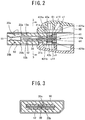
Fig. 2 is a cross-sectional schematic view of the connector, taken along line 2-2 ofFig. 1(c) . -
Fig. 3 is a schematic end view of the connector, taken along line 3-3 ofFig. 2 . -
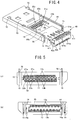
Fig. 4 is an exploded perspective schematic view of a housing, a conductive member, and a lead connection assisting member of the connector. -
Figs. 5(a) and 5(b) are schematic views of the housing of the connector, whereinFig. 5(a) is a front view of the housing with contacts and the conductive member attached thereto, andFig. 5(b) is a rear view thereof. -
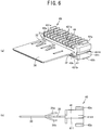
Figs. 6(a) and 6(b) are schematic views of the conductive member and the lead connection assisting member of the connector, whereinFig. 6(a) is a perspective view, andFig 6(b) is a side view. -
Figs. 7(a) and 7(b) are schematic views of the lead connection assisting member of the connector, whereinFig. 7(a) is a rear view, andFig. 7(b) is an enlarged view of an area X indicated inFig. 7(a) . -
Fig. 8 is a schematic cross-sectional view of the connector coupled to a receptacle connector. Description of Embodiments - Electrical connectors according to the present invention will be described below.
- An electrical connector according to the present invention is described below with reference to the drawings.
Figs. 1(a) to 1(c) are schematic views of the electrical connector, whereinFig. 1(a) is a perspective view,Fig. 1(b) is a side view, andFig. 1(c) is a plan view.Fig. 2 is a cross-sectional schematic view of the connector, taken along line 2-2 ofFig. 1(c) .Fig. 3 is a schematic end view of the connector, taken along line 3-3 ofFig. 2 .Fig. 4 is an exploded perspective schematic view of a housing, a conductive member, and a lead connection assisting member of the connector.Figs. 5(a) and 5(b) are schematic views of the housing of the connector, whereinFig. 5(a) is a front view of the housing with contacts and the conductive member attached thereto, andFig. 5(b) is a rear view.Figs. 6(a) and 6(b) are schematic views of the conductive member and the lead connection assisting member of the connector, whereinFig. 6(a) is a perspective view, andFig 6(b) is a side view.Figs. 7(a) and 7(b) are schematic views of the lead connection assisting member of the connector, whereinFig. 7(a) is a rear view, andFig. 7(b) is an enlarged view of
an area X indicated inFig. 7(a) .Fig. 8 is a schematic cross-sectional view of the connector coupled to a receptacle connector. - The electrical connector as shown in
Figs. 1(a) and 1(b) is a plug connector referred to as DisplayPort, adapted for attachment to a leading end of a bulk cable c for use in high speed signaling. The electrical connector includes ahousing 10, first andsecond contact groups conductive member 30, a leadconnection assisting member 40, ashield cover 50, and acase 60. Each component of the connector will be described below in detail. - As shown in
Figs. 1(a) to 5(b) , thehousing 10 is a molded article of insulative resin. Thehousing 10 has a main body of generally rectangular parallelepiped shape. The leading end of the main body has anopening 11. The rear end of the main body has a receivinghole 12 communicating with theopening 11. Moreover, a plurality of upper and lowercontact containing grooves opening 11 and the receivinghole 12 of the main body. A pair of guide plates 14 (guide means) is provided at widthwise ends of the rear end face of the main body. A pair of lockterminal containing grooves 15 is formed along the widthwise ends the main body and along theguide plates 14. - The
opening 11 is a generally rectangular hole opening frontward to receive a connecting protrusion R1 (seeFig. 8 ) of a receptacle connector R of an electronic instrument etc. - The receiving
hole 12 is a generally rectangular hole opening rearward to receive theconductive member 30. - As shown in
Fig. 2 , the upper and lowercontact containing grooves housing 10 and communicate with theopening 11 and the receivinghole 12. The uppercontact containing grooves 13a are arranged out of phase with the lowercontact containing grooves 13b, as shown inFigs. 5(a) and 5(b) . The upper and lowercontact containing grooves second contact groups contact containing grooves second contact groups hole 12 in thehousing 10. - As shown in
Fig. 4 , pairedguide projections 14a are provided on the inner surfaces of theguide plates 14. Theguide projections 14a fit in paired guide recesses 411 formed along the lateral edges of the leadconnection assisting member 40, so that the leadconnection assisting member 40 is guided toward the rear end of the main body of thehousing 10. -
Lock terminals 70, generally U shaped resilient metal bodies, are inserted for attachment into the lockterminal containing grooves 15. The leading ends of thelock terminals 70 are thus able to rise from and sink into the lockterminal containing grooves 15. - As shown in
Figs. 2 to 5(b) , thefirst contact group 20a includes a plurality of signalingcontacts 21a andground contacts 22a. The signalingcontacts 21a and theground contacts 22a, which are the same metal plates having leading ends bent in a generally V-shape, are contained in the uppercontact containing grooves 13a so as to be arranged in line along the width of thehousing 10. When the signalingcontacts 21a and theground contacts 22a are arranged in place, their leading ends are situated in an upper part of theopening 11 in thehousing 10, and their middle portions are situated above the receivinghole 12 in thehousing 10. As shown inFig. 4 , the rear end portions of the signalingcontacts 21a and of theground contacts 22a project out of the rear face of the main body of thehousing 10. These rear end portions constitute connection portions to be soldered to cores c11 that are taken from a plurality of lead wires c1 incorporated in the cable c, as illustrated inFig. 2 . - The
second contact group 20b also includes a plurality of signalingcontacts 21b andground contacts 22b. The signalingcontacts 21b and theground contacts 22b, which are the same metal plates having leading ends bent in a generally V-shape, are contained in the lowercontact containing grooves 13b so as to be arranged in line along the width of thehousing 10. When the signalingcontacts 21b and theground contacts 22b are arranged in place, their leading ends are situated in a lower part of theopening 11 in thehousing 10 and their middle portions are situated below the receivinghole 12 in thehousing 10. As shown inFig. 4 , the rear end portions of the signalingcontacts 21b and of theground contacts 22b project out of the rear surface of the main body of thehousing 10. These rear end portions constitute connection portions to be soldered with cores c11 that are taken from lead wires c1 incorporated in the cable c, as illustrated inFig. 2 , . - As shown in
Figs. 2, 3 ,5(a) ,6(a) and 6(b) , theconductive member 30 is a generally rectangular metal plate formed by press forming. It is inserted into the receivinghole 12 in thehousing 10 to be interposed between the first andsecond contact groups conductive member 30 has a leading end portion (a first crosstalk reducer) to be received in the receivinghole 12 in thehousing 10 and a rear end portion (a second crosstalk reducer) to be fitted in anattachment hole 44 in the leadconnection assisting member 40. - The leading end portion of the
conductive member 30 has a length dimension that is substantially equal to the length dimension of the middle portions of the signalingcontacts ground contacts conductive member 30 has a length dimension that is larger than the length dimension of the rear end portions of the signalingcontacts ground contacts - In the leading end portion of the
conductive member 30, its rear area is cut at portions to form two cut-and-raisedpieces 31a bent upward (to serve as grounding portions in the form of projections) and three cut-and-raisedpieces 31b bent downward (to serve as grounding portions in the form of projections). The cut-and-raisedpieces ground contacts conductive member 30 received in the receivinghole 12 in thehousing 10. It should be noted that the rear area is cut out at said portions so as not to produce substantial gaps between the end faces of the portions to become the cut-and-raisedpieces pieces conductive member 30 from being impaired due to signal leaks through the gaps, which signals are generated between the signalingcontacts 21a of thefirst contact group 20a and the signalingcontacts 21b of thesecond contact group 20b. - The widthwise ends in the rear area are provided with paired locking projections 32 (first locking means). The widthwise dimension of the rear area including the paired locking
projections 32 is slightly larger than the widthwise dimension of the receivinghole 12 of thehousing 10. Accordingly, when the leading end portion of theconductive member 30 is press-fitted into the receivinghole 12 of thehousing 10, the pair of lockingprojections 32 is locked in the receivinghole 12 of thehousing 10. The press-fittedconductive member 30 is disposed as shown inFig. 2 , i.e., it runs parallel to the middle portions and rear end portions of the contacts of the first andsecond contact groups - As shown in
Figs. 2 ,4 ,6(a) and 6(b) , the leadconnection assisting member 40 is a molded article of insulative resin, and it is attached to the rear end of thehousing 10. The leadconnection assisting member 40 has a generallyrectangular parallelepiped base 41, a firstvertical wall 42a and a secondvertical wall 42b that are provided upright on the upper and lower surfaces, respectively, of the rear end of thebase 41, a first support table 43a and a second support table 43b of rectangular plate-like shape that are provided on the upper and lower surfaces of the leading end of thebase 41, and the generallyrectangular attachment hole 44 formed in the leading end face of thebase 41. - The
base 41 is provided in its lateral faces with the guide recesses 411 to receive the pair ofguide projections 14a of thehousing 10. The guide recesses 411 each have, on their upper and lower surfaces in the rearmost portions, locking projections 4111 (second locking means). The distance between the upper andlower locking projections 4111 is slightly smaller than the thickness dimension of theguide projections 14a. As such, theguide projections 14a inserted into the guide recesses 411 are press fitted between the upper andlower locking projections 4111, so that the leadconnection assisting member 40 is securely attached to the rear end of thehousing 10. As theguide projections 14a guide the guide recesses 411, the leadconnection assisting member 40 can be easily attached to the rear end of thehousing 10, theconductive member 30 can be easily inserted in position in the receivinghole 12 in thehousing 10. - As shown in
Figs. 2 ,6(a) ,6(b) ,7(a), and 7(b) , the firstvertical wall 42a is provided with a plurality of firstlead insertion grooves 421a at an equal pitch distance to the pitch distance of the signalingcontacts 21a and theground contacts 22a. The firstlead insertion grooves 421a are used to receive and temporally hold the leading ends of the lead wires c1 of the cable c. The firstlead insertion grooves 421a are slightly smaller in lateral dimension than the leading ends of the lead wires c1 so as to press-fit and hold therein the leading ends of the lead wires c1. Moreover, the firstlead insertion grooves 421a are each provided at their ends on the open side withbarbs - The second
vertical wall 42b is provided with a plurality of secondlead insertion grooves 421b at an equal pitch distance to the pitch distance of the signalingcontacts 21b and theground contacts 22b. The secondlead insertion grooves 421b are used to receive and temporally hold the leading ends of the lead wires c1 of the cable c. The secondlead insertion grooves 421b shall not be described in detail because they have the same configuration as the firstlead insertion grooves 421a. - As shown in
Figs. 2 and6(a) , the first support table 43a serves to provide support for soldering the rear end portions of the signalingcontacts 21a and of theground contacts 22a to the cores c11 taken from the leading ends of the lead wires c1 of the cable c. The surface of the first support table 43a is provided with a plurality offirst guide grooves 431a for guiding the rear end portions of the signalingcontacts 21a and of theground contacts 22a, in communication with the firstlead insertion grooves 421a. - The second support table 43b serves to provide support for soldering the rear end portions of the signaling
contacts 21b and of theground contacts 22b to the cores c11 taken from the leading ends of the lead wires c1 of the cable c. The surface of the second support table 43b is provided with a plurality ofsecond guide grooves 431b for guiding the rear end portions of the signalingcontacts 21b and of theground contacts 22b, in communication with the secondlead insertion grooves 421b. - As shown in
Fig. 2 , the depth of theattachment hole 44 is defined from the leading end face of the base 41 to a portion between the first and secondvertical walls conductive member 30 fitted in theattachment hole 44 is located in the space below the first support table 43a and the firstlead insertion grooves 421a and above the second support table 43b and the secondlead insertion grooves 421b. In other words, the rear end portion of theconductive member 30 is located in the space below the signalingcontacts 21a and the cores c11 of the lead wires c1 of the cable c soldered thereto and above the signalingcontacts 21b and the cores c11 of the lead wires c1 of the cable c soldered thereto, thereby reducing crosstalk generated therebetween. - As shown in
Figs. 1(a) to 1(c) and2 , theshield cover 50 is a rectangular tuboid shell that covers the outer peripheral surfaces of thehousing 10. In a front portion on the upper surface of theshield cover 50, there are formed side by side pairedholes 51, for passing the leading ends of thelock terminals 70 therethrough, and lockingholes 52, for locking locking portions of the receptacle connector R. - The
case 60 is a resin-molded body that houses thehousing 10 and theshield cover 50 and protects the proximal end of theshield cover 50. Apress button 61 is disposed on the upper surface of thecase 60 for switching between lock and release of the receptacle connector. More specifically, inside thecase 60, thepress button 61 is coupled to the proximal ends of thelock terminals 70, allowing the leading ends of thelock terminals 70 to move up and down. - The electrical connector having components as described above is assembled in the following steps. First, the signaling
contacts 21a and theground contacts 22a are press-fitted into the uppercontact containing grooves 13a in thehousing 10. Similarly, the signalingcontacts 21b and theground contacts 22b are press-fitted into the lowercontact containing grooves 13b in thehousing 10. In this state, the rear end portions of the signalingcontacts 21a and of theground contacts 22a project from the rear surface of the main body of thehousing 10, and the rear end portions of the signalingcontacts 21b and of theground contacts 22b project from the rear surface of the main body of thehousing 10. The signalingcontacts 21a and theground contacts 22a are thus arranged above the receivinghole 12 in thehousing 10, out of phase with the signalingcontacts 21b and theground contacts 22b below the receivinghole 12. - After that, the rear end portion of the
conductive member 30 is fitted into theattachment hole 44 in the leadconnection assisting member 40. The leading end portion of theconductive member 30 is then inserted into the receivinghole 12 in thehousing 10, while the pair ofguide projections 14a of thehousing 10 is inserted into the pair of guide recesses 411 on the leadconnection assisting member 40. Then the cut-and-raisedpieces conductive member 30 are brought into contact with therespective ground contacts conductive member 30 and theground contacts - At this point, the pair of locking
projections 32 of theconductive member 30 are press-fitted against the lateral surfaces of the receivinghole 12, and the pair ofguide projections 14a is each press-fitted between the upper andlower locking projections 4111 formed in each of the paired guide recesses 411 of the leadconnection assisting member 40. As a result, the leading end portion of theconductive member 30 is received and securely placed in position in the receivinghole 12 in thehousing 10, and the leading end portion is interposed between the middle portions (of the signalingcontacts 21a and of theground contacts 22a) and the middle portions (of the signalingcontacts 21b and of theground contacts 22b). Also, the leadconnection assisting member 40 is securely attached to the rear end of thehousing 10. - Further, the signaling
contacts 21a and theground contacts 22a that project out of the rear surface of the main body of thehousing 10 are received in thefirst guide grooves 431a of the leadconnection assisting member 40 to be disposed on the first support table 43a. Similarly, the signalingcontacts 21b and theground contacts 22b are received in thesecond guide grooves 431b of the leadconnection assisting member 40 to be disposed on the second support table 43b. - After that, the cores c11 are taken from the leading ends of the lead wires c1 of the cable c. The leading ends of the lead wires c1 are press-fitted into the first and second
lead insertion grooves connection assisting member 40, and the cores c11 of the lead wires c1 are placed on the first and second support tables 43a and 43b. - Then, collective soldering by a pulse heating method etc. is performed on the first support table 43a to connect the signaling
contacts 21a and theground contacts 22a with the cores c11 of the lead wires c1, and also on the second support table 43b to connect the signalingcontacts 21b and theground contacts 22b with the cores c11 of the lead wires c1. After soldering, the rear end portion of theconductive member 30 is located below the rear end portions of the signalingcontacts 21a and of theground contacts 22a and the cores c11 soldered thereto, and above the rear end portions of the signalingcontacts 21b and of theground contacts 22b and the cores c11 soldered thereto. - The
housing 10 in this state is inserted into theshield cover 50. Thecase 60 is then molded over the proximal end of theshield cover 50. - The electrical connector thus assembled is used in the following manner. First, the connecting protrusion R1 of the receptacle connector R is inserted into the
opening 11 in the electrical connector. As shown inFig. 8 , the inserted connection protrusion R1 presses upward the leading ends of the signalingcontacts 21a and of theground contacts 22a of the electrical connector into elastic contact with the upper contacts R11. Simultaneously, the connection protrusion R1 presses downward the leading ends of the signalingcontacts 21b and of theground contacts 22b into elastic contact with the lower contacts R12. As a result, the lead wires c1 and the signalingcontacts conductive member 30 and theground contacts - In the electrical connector as described above, simply inserting the
conductive member 30 into the receivinghole 12 in thehousing 10 brings the cut-and-raisedpieces conductive member 30 into contact with theground contacts ground contacts conductive member 30 and theground contacts conductive member 30 without providing thehousing 10 as a two-piece structure and without boring guiding holes in thehousing 10, so that the electrical connector can be simplified in structure. - Further, crosstalk is less likely to occur between the middle portions of the signaling
contacts 21a and the middle portions of the signalingcontacts 21b because the leading end portion of theconductive member 30 is received in the receivinghole 12 in thehousing 10 to be interposed between the middle portions of the signalingcontacts 21a and of theground contacts 22a and the middle portions of the signalingcontacts 21b and of theground contacts 22b. In addition, the rear end portion of theconductive member 30 is fittingly received in theattachment hole 44 in the leadconnection assisting member 40 so as to be interposed in the space below the rear end portions of the signalingcontacts 21a and of theground contacts 22a as well as the cores c11 of the upper lead wires c1 that are soldered to these rear end portions, and above the rear end portions of the signalingcontacts 21b and of theground contacts 22b as well as the cores c11 of the lower lead wires c1 that are soldered to these rear end portions. Hence, the rear end portion of theconductive member 30 also serves to reduce crosstalk between the rear end portions of the signalingcontacts 21a as well as the cores c11 of the upper lead wires c1 and the rear end portions of the signalingcontacts 21b as well as the cores c11 of the lower lead wires c1. Moreover, eachground contact 22a is disposed among a predetermined number of signalingcontacts 21a, and eachground contact 22b is also disposed among a predetermined number of signalingcontacts 21b, thereby reducing crosstalk among the signalingcontacts 21a and among the signalingcontacts 21b. - Furthermore, crosstalk can be further reduced by electrically connecting the cut-and-raised
pieces conductive member 30 to the ground pattern on the board through theground contacts ground contacts - Further advantageously, the first and second
lead insertion grooves connection assisting member 40 allow the leading ends of the lead wires c1 of the cable c to be temporarily held on the back side of thehousing 10. In this state, a single collective soldering using a pulse heating method or the like is made to connect the cores c11 that are taken from the leading ends of the lead wires c1 with the rear end portions of the signalingcontacts ground contacts housing 10, supported on the first and second support tables 43a and 43b of the leadconnection assisting member 40. It is thus advantageously easy to assemble the electrical connector, leading to improved mass productivity. - The
barbs 422a and 422b serves not only to prevent the leading ends of the lead wires c1 of the cable c from readily slipping out of the first and secondlead insertion grooves lead insertion grooves connection assisting member 40 and can be accordingly soldered with extremely high accuracy. The present electrical connector thus offers outstanding performance because of its improved transmission characteristics. - Further, the
conductive member 30 received in the receivinghole 12 of thehousing 10 serves to protect thehousing 10 from distortion. The pair ofguide plates 14 of thehousing 10 is also reinforced by placing the leadconnection assisting member 40 between theguide plates 14. The mechanical strength of the entire electrical connector is thus improved, hence enabling downsizing of the electrical connector. - The above-described electrical connector may be modified without departing from the scope of the claims. Possible modifications to each component are described in detail below.
- The
housing 10 may be modified appropriately as long as thehousing 10 has at least one receiving hole and allows first and second contact groups to be arranged on opposite sides of the receiving hole. It is therefore possible to provide two or more receiving holes in the housing for arranging therein three or more rows of contact groups. The first and second contact groups may be embedded on opposite sides of the receiving hole of the housing. - The
guide projections 14a are provided on the inner surfaces of the pairedguide plates 14, but it is also possible to provide guide recesses. In this case, guide projections may be provided on the opposite ends of thebase 41 of the leadconnection assisting member 40. Theguide plates 14 may be omitted or may have any other shape other than the plate-like shape. In this case, the leadconnection assisting member 40 can be attached to the rear end of thehousing 10 by other means, e.g., by fitting theconductive member 30 into the receivinghole 12 in thehousing 10. - Any kind of
conductive member 30 may be used as long as it is received in a receiving hole in the housing to be contactable with ground contacts of the first and second contact groups. For example, the conductive member may be fabricated by coating non-conductive material, such as synthetic resin, with metal by vapor deposition or some other method. - The leading end portion of the
conductive member 30 serves as the first crosstalk reducer and the rear end portion thereof serves as the second crosstalk reducer, but the present invention is not limited thereto. For example, the entireconductive member 30 may be the first crosstalk reducer. In this case, the leading end portion of theconductive member 30 is extended up to a position between the leading ends of the signaling contacts of the first and second contact groups. - The
conductive member 30 has the cut-and-raisedpieces - The
conductive member 30 only needs to contact at least one ground contact of the first and second contact groups. The conductive member of course may be connected to all ground contacts of the first and second contact groups. - The cut-and-raised
pieces conductive member 30 is not affected. - It is optional whether to provide the paired locking
projections 32 on opposite lateral ends of theconductive member 30, serving as the first locking means. The first locking means need not be provided on theconductive member 30, and it may be provided as a locking projection on a lateral surface of the receivinghole 12 in thehousing 10. The first locking means may be provided both on the conductive member and on the lateral surfaces of the receivinghole 12 in thehousing 10. Any other well-known locking means, such as a combination of a locking projection and a locking recess, may be employed. - The signaling contacts are directly or indirectly soldered at their rear end portions to the cores of the lead wires, but the present invention is not limited thereto. As later described in detail, when the electrical connector is a plug connector other than the type having a cable connected thereto, or a receptacle connector, the rear end portions of the contacts may be connected to conductors or other connection objects of a circuit board of an electronic instrument or the like. Moreover, as to the ground contacts, at least one should be included in the first and second contact groups. In the above-described contacts, portions other than the rear end portions can be used as connecting portions for connection with the conductors of the cable or the multilayer board.
- The lead
connection assisting member 40 may be appropriately modified, provided the lead connection assisting member includes first and second support tables for supporting the rear end portions of signaling contacts of first and second contact groups and cores taken from the leading ends of lead wires so that soldering of the contact rear end portions with the cores can be performed on the support tables, the assisting member also including, on the rear end sides of the first and second support tables, a plurality of first and second lead insertion grooves that are arranged at equal pitch intervals to the pitch intervals of the signaling contacts of the first and second contact groups, for receiving and temporarily holding the leading ends of the lead wires. The leadconnection assisting member 40 may be omitted, and particularly if the electrical connector is a plug connector which is not of a type involving cable connection, or a receptacle connector, as described later. - The first and second
lead insertion grooves second guide grooves second guide grooves - The present invention is not limited to the locking
projections 4111 serving as the second locking means that lock the lead connection assisting member as guided by the guide means and as attached to the rear end of the housing. For example, locking projections may be provided on theguide projections 14a on theguide plates 14. Alternatively, locking projections may be provided on both theguide projections 14a and the guide recesses 411 of the leadconnection assisting member 40. It is also possible to provide the second locking means in some other area than theguide projections 14a or the guide recesses 411 of the lead connection assisting member. The leadconnection assisting member 40 may be provided integrally on the rear end of thehousing 10. The second locking means may be provided as any other well-known locking means, such as a combination of a locking projection and a locking recess. - The electrical connector of the present invention is not limited to the foregoing embodiments with respect to the kinds, shapes, materials of its components, the number of pins, etc. The electrical connector is not limited to a DisplayPort or like plug connector and is applicable to plug connectors of types without a cable connected thereto or to receptacle connectors. The cable c is not limited to a bulk cable, and any other similar cable may be used.
Claims (7)
- An electrical connector comprising:a housing (10) having an opening (11) configured to receive a mating connector and a receiving hole (12) communicating with the opening;a first contact group (20a) and a second contact group (20b), each contact group comprising a number of elongate contact elements (21a, 22a, 23a; 21b, 22b, 23b) extending parallel to the insertion direction and arranged in a line along the width of the housing, the respective groups being arranged along opposite sides of the receiving hole in the housing; anda conductive member (30) received in the receiving hole,wherein the first and second contact groups include signaling contacts (21a, 21b), and at least one of the first and second contact groups further includes a ground contact (22a, 22b);
characterised in that a leading end portion of the conductive member is disposed in the receiving hole in a space between middle portions of the signaling contacts (21a) of the first contact group and middle portions of the signaling contacts (21b) of the second contact group;and in that electrical connection is made between the conductive member and the ground contact (22a, 22b) within the receiving hole (12). - The electrical connector according to claim 1, wherein the conductive member (30) includes a grounding portion (31a, 31b) in the form of a projection that is in contact with the ground contact
(22a, 22b). - The electrical connector according to claim 2, wherein
the conductive member (30) comprises a metal plate, and
the grounding portion comprises a cut-and-raised piece (31a, 31b) formed by cutting and bending a portion of the conductive member. - The electrical connector according to claim 2, wherein the conductive member (30) comprises a plate-like non-conductive material with peripheral surfaces thereof coated with metal, and
the grounding portion (31a, 31b) comprises the projection provided on the non-conductive material and coated with the metal. - The electrical connector according to claim 2, wherein first locking means (32) for locking the conductive member (30) received in the receiving hole (12) of the housing (10) is provided on at least one of an inner surface of the receiving hole in the housing and the conductive member.
- The electrical connector according to claim 1, wherein the conductive member (30) includes:a first crosstalk reducer constituted by said leading end portion; anda second crosstalk reducer on a rear end side thereof, being interposed between rear end portions of the signaling contacts (21a) of the first contact group (20a) and rear end portions of the signaling contacts (21b) of the second contact group (20b).
- The electrical connector according to claim 6, being connectable with a plurality of lead wires (c11) and further comprising a lead connection assisting member (40) provided at a rear end of the housing (10), wherein the signaling contacts (21a, 21b) of the first (20a) and second (20b) contact groups have the middle portions arranged on the opposite sides of the receiving hole (12) of the housing and have the rear end portions projecting out of a rear surface of the housing,
the lead connection assisting member includes: first (43a) and second (43b) support tables for providing support in soldering the rear end portions of the signaling contacts (21a, 21b) of the first (20a) and second (20b) contact groups to cores (c11) taken from leading ends of the lead wires; and
first lead insertion grooves (421a) and second lead insertion grooves (421b) provided on rear end sides of the first support table (43a) and second support table (43b), respectively, the first and second lead insertion grooves being arranged at equal pitch distance to the pitch distance of the signaling contacts (21a, 21b) of the first (20a) and second (20b) contact groups, the first and second lead insertion grooves being adapted to receive and temporarily hold the respective leading ends of the lead wires,
the first crosstalk reducer is received in the receiving hole (12) in the housing (10), and
the second crosstalk reducer is interposed between a portion of the lead connection assisting member (40) including the first support table (43a) and the first lead insertion grooves (421a) and a portion of the lead connection assisting member (40) including the second support table (43b) and the second lead insertion grooves (421b) of the lead connection assisting member.
Priority Applications (1)
| Application Number | Priority Date | Filing Date | Title |
|---|---|---|---|
| EP15162093.7A EP2922154B1 (en) | 2008-06-04 | 2009-05-19 | Electrical connector |
Applications Claiming Priority (2)
| Application Number | Priority Date | Filing Date | Title |
|---|---|---|---|
| JP2008146991 | 2008-06-04 | ||
| PCT/JP2009/002204 WO2009147791A1 (en) | 2008-06-04 | 2009-05-19 | Electric connector |
Related Child Applications (2)
| Application Number | Title | Priority Date | Filing Date |
|---|---|---|---|
| EP15162093.7A Division EP2922154B1 (en) | 2008-06-04 | 2009-05-19 | Electrical connector |
| EP15162093.7A Division-Into EP2922154B1 (en) | 2008-06-04 | 2009-05-19 | Electrical connector |
Publications (3)
| Publication Number | Publication Date |
|---|---|
| EP2293393A1 EP2293393A1 (en) | 2011-03-09 |
| EP2293393A4 EP2293393A4 (en) | 2011-11-02 |
| EP2293393B1 true EP2293393B1 (en) | 2020-01-15 |
Family
ID=41397878
Family Applications (2)
| Application Number | Title | Priority Date | Filing Date |
|---|---|---|---|
| EP15162093.7A Active EP2922154B1 (en) | 2008-06-04 | 2009-05-19 | Electrical connector |
| EP09758058.3A Active EP2293393B1 (en) | 2008-06-04 | 2009-05-19 | Electric connector |
Family Applications Before (1)
| Application Number | Title | Priority Date | Filing Date |
|---|---|---|---|
| EP15162093.7A Active EP2922154B1 (en) | 2008-06-04 | 2009-05-19 | Electrical connector |
Country Status (8)
| Country | Link |
|---|---|
| US (1) | US8262411B2 (en) |
| EP (2) | EP2922154B1 (en) |
| JP (1) | JP5197742B2 (en) |
| KR (1) | KR101578791B1 (en) |
| CN (1) | CN102047507B (en) |
| ES (2) | ES2749632T3 (en) |
| TW (1) | TWI442650B (en) |
| WO (1) | WO2009147791A1 (en) |
Families Citing this family (113)
| Publication number | Priority date | Publication date | Assignee | Title |
|---|---|---|---|---|
| CN104319557B (en) * | 2009-11-06 | 2017-06-23 | 莫列斯公司 | Electric connector |
| US8740647B1 (en) * | 2010-02-02 | 2014-06-03 | Arris Enterprises, Inc. | Reduced crosstalk in a multi-channel conductive body connector |
| CN201698051U (en) * | 2010-02-09 | 2011-01-05 | 富士康(昆山)电脑接插件有限公司 | Cable connector |
| CN102480070B (en) * | 2010-11-22 | 2016-02-03 | 富士康(昆山)电脑接插件有限公司 | Wire and cable connector and manufacture method thereof and method for transmitting signals |
| JP5209038B2 (en) * | 2010-12-08 | 2013-06-12 | 日立オートモティブシステムズ株式会社 | Connector and manufacturing method thereof |
| JP5707913B2 (en) * | 2010-12-09 | 2015-04-30 | ソニー株式会社 | Transmitter and receiver |
| JP5811460B2 (en) * | 2012-02-15 | 2015-11-11 | ホシデン株式会社 | connector |
| US9252542B2 (en) * | 2012-05-24 | 2016-02-02 | Foxconn Interconnect Technology Limited | Electrical connector with shielding plate thereof |
| TWI574467B (en) * | 2012-06-29 | 2017-03-11 | 鴻海精密工業股份有限公司 | Electrical connector and assmbly of the same |
| US9525227B2 (en) | 2012-07-21 | 2016-12-20 | Foxconn Interconnect Technology Limited | Flippable electrical connector |
| US9716327B2 (en) * | 2012-09-28 | 2017-07-25 | Intel Corporation | System, circuit module, and circuit module connector |
| TWI514693B (en) * | 2012-10-18 | 2015-12-21 | Hon Hai Prec Ind Co Ltd | An electrical connector plug can be forward or reverse connected and assembly thereof |
| TWI593199B (en) * | 2013-01-08 | 2017-07-21 | 鴻騰精密科技股份有限公司 | Electrical connector |
| WO2014113563A1 (en) * | 2013-01-16 | 2014-07-24 | Molex Incorporated | Low profile connector system |
| US8851927B2 (en) | 2013-02-02 | 2014-10-07 | Hon Hai Precision Industry Co., Ltd. | Electrical connector with shielding and grounding features thereof |
| US8864506B2 (en) | 2013-03-04 | 2014-10-21 | Hon Hai Precision Industry Co., Ltd. | Cable connector with improved grounding plate |
| CN105531875B (en) * | 2013-03-13 | 2017-09-05 | 莫列斯有限公司 | Signal is to unit and using connector of the signal to unit |
| US8961194B2 (en) * | 2013-03-14 | 2015-02-24 | Bby Solutions, Inc. | Active HDMI connector with integrated design |
| CN203225389U (en) * | 2013-04-12 | 2013-10-02 | 富士康(昆山)电脑接插件有限公司 | Electric connector assembly |
| CN203445352U (en) | 2013-06-28 | 2014-02-19 | 富士康(昆山)电脑接插件有限公司 | Electric connector |
| US9490594B2 (en) | 2013-07-19 | 2016-11-08 | Foxconn Interconnect Technology Limited | Flippable electrical connector |
| US9490595B2 (en) | 2013-07-19 | 2016-11-08 | Foxconn Interconnect Technology Limited | Flippable electrical connector |
| US10170870B2 (en) | 2013-07-19 | 2019-01-01 | Foxconn Interconnect Technology Limited | Flippable electrical connector |
| US10693261B2 (en) | 2013-07-19 | 2020-06-23 | Foxconn Interconnect Technology Limited | Flippable electrical connector |
| US9356400B2 (en) | 2013-07-19 | 2016-05-31 | Foxconn Interconnect Technology Limited | Flippable electrical connector |
| US9496662B2 (en) | 2013-07-19 | 2016-11-15 | Foxconn Interconnect Technology Limited | Flippable electrical connector |
| US9525223B2 (en) | 2013-07-19 | 2016-12-20 | Foxconn Interconnect Technology Limited | Flippable electrical connector |
| US9496664B2 (en) | 2013-07-19 | 2016-11-15 | Foxconn Interconnect Technology Limited | Flippable electrical connector |
| US9472910B2 (en) | 2013-07-19 | 2016-10-18 | Foxconn Interconnect Technology Limited | Flippable electrical connector |
| US9912111B2 (en) | 2013-07-19 | 2018-03-06 | Foxconn Interconnect Technology Limited | Flippable electrical connector |
| US9520677B2 (en) | 2013-07-19 | 2016-12-13 | Foxconn Interconnect Technology Limited | Flippable electrical connector |
| US10720734B2 (en) * | 2013-07-19 | 2020-07-21 | Foxconn Interconnect Technology Limited | Flippable electrical connector |
| US9496653B2 (en) | 2013-07-19 | 2016-11-15 | Foxconn Interconnect Technology Limited | Flippable electrical connector |
| US9660400B2 (en) | 2013-07-19 | 2017-05-23 | Foxconn Interconnect Technology Limited | Flippable electrical connector |
| US9466930B2 (en) | 2013-07-19 | 2016-10-11 | Foxconn Interconnect Technology Limited | Flippable electrical connector |
| US10826255B2 (en) | 2013-07-19 | 2020-11-03 | Foxconn Interconnect Technology Limited | Flippable electrical connector |
| US9843148B2 (en) | 2013-07-19 | 2017-12-12 | Foxconn Interconnect Technology Limited | Flippable electrical connector |
| US9490584B2 (en) | 2013-07-19 | 2016-11-08 | Foxconn Interconnect Technology Limited | Flippable electrical connector |
| US9997853B2 (en) | 2013-07-19 | 2018-06-12 | Foxconn Interconnect Technology Limited | Flippable electrical connector |
| US9502821B2 (en) | 2013-07-19 | 2016-11-22 | Foxconn Interconnect Technology Limited | Flippable electrical connector |
| US9905944B2 (en) | 2013-07-19 | 2018-02-27 | Foxconn Interconnect Technology Limited | Flippable electrical connector |
| US9490579B2 (en) | 2013-07-19 | 2016-11-08 | Foxconn Interconnect Technology Limited | Flippable Electrical Connector |
| US9755368B2 (en) | 2013-07-19 | 2017-09-05 | Foxconn Interconnect Technology Limited | Flippable electrical connector |
| US9281629B2 (en) | 2013-07-19 | 2016-03-08 | Foxconn Interconnect Technology Limited | Flippable electrical connector |
| US9472911B2 (en) | 2013-07-19 | 2016-10-18 | Foxconn Interconnect Technology Limited | Flippable electrical connector with concentric inner and outer mating ports |
| US9484681B2 (en) | 2013-07-19 | 2016-11-01 | Foxconn Interconnect Technology Limited | Flippable electrical connector |
| US9350126B2 (en) | 2013-07-19 | 2016-05-24 | Foxconn Interconnect Technology Limited | Electrical connector having a receptacle with a shielding plate and a mating plug with metallic side arms |
| CN104425995B (en) * | 2013-09-06 | 2017-01-18 | 富士康(昆山)电脑接插件有限公司 | Electrical connector and assembly thereof |
| US9400529B2 (en) | 2013-09-27 | 2016-07-26 | Apple Inc. | Electronic device having housing with embedded interconnects |
| DE102013225794A1 (en) * | 2013-12-12 | 2015-06-18 | Leoni Kabel Holding Gmbh | Contact connection of shielded data lines on a circuit board and method for contacting a plurality of shielded data lines on a circuit board |
| US9454177B2 (en) | 2014-02-14 | 2016-09-27 | Apple Inc. | Electronic devices with housing-based interconnects and coupling structures |
| CN204361415U (en) * | 2014-02-17 | 2015-05-27 | 富士康(昆山)电脑接插件有限公司 | Pin connector |
| JP2015159092A (en) * | 2014-02-25 | 2015-09-03 | 矢崎総業株式会社 | connection terminal |
| JP6368504B2 (en) | 2014-03-07 | 2018-08-01 | 宏致電子股▲ふん▼有限公司Aces Electronics Co.,Ltd. | Electrical connector |
| JP6265803B2 (en) | 2014-03-19 | 2018-01-24 | 日本航空電子工業株式会社 | connector |
| TWI609530B (en) * | 2014-03-24 | 2017-12-21 | 連展科技股份有限公司 | Electrical connector assembly |
| TWI504082B (en) * | 2014-04-21 | 2015-10-11 | Advanced Connectek Inc | Socket electrical connector and plug electrical connector |
| CN106415944A (en) | 2014-04-23 | 2017-02-15 | 泰科电子公司 | Electrical connector with shield cap and shielded terminals |
| TWI600236B (en) * | 2014-05-07 | 2017-09-21 | 鴻騰精密科技股份有限公司 | Electrical connector and method for making the same |
| US9722383B2 (en) | 2014-05-07 | 2017-08-01 | Foxconn Interconnect Technology Limited | Electrical connector having insulative housing and method of making the same |
| TWI556522B (en) * | 2014-05-22 | 2016-11-01 | Advanced Connectek Inc | Socket electrical connector and plug electrical connector |
| CN105337082B (en) * | 2014-06-09 | 2018-05-04 | 富士康(昆山)电脑接插件有限公司 | Connector assembly and its manufacture method |
| JP6265852B2 (en) * | 2014-07-08 | 2018-01-24 | 日本航空電子工業株式会社 | connector |
| TWI618305B (en) | 2014-08-11 | 2018-03-11 | 英屬開曼群島商鴻騰精密科技股份有限公司 | Electrical connector and a manufacturing method thereof |
| TWI573335B (en) | 2014-08-13 | 2017-03-01 | 鴻騰精密科技股份有限公司 | Electrical connector and method of making the same |
| JP6590472B2 (en) * | 2014-08-20 | 2019-10-16 | 住友電気工業株式会社 | Signal transmission cable terminal structure |
| TWI578633B (en) * | 2014-08-22 | 2017-04-11 | 鴻騰精密科技股份有限公司 | Electrical connector and method of making the same |
| CN104241891B (en) * | 2014-09-04 | 2017-04-19 | 深圳市江波龙电子有限公司 | Electronic device production method |
| US9520670B2 (en) * | 2014-09-23 | 2016-12-13 | Hubbell Incorporated | Tamper resistant receptacle |
| JP6359410B2 (en) * | 2014-10-02 | 2018-07-18 | ホシデン株式会社 | connector |
| CN104518321B (en) * | 2014-11-27 | 2023-05-05 | 连展科技电子(昆山)有限公司 | Plug electric connector |
| TWM497873U (en) * | 2014-12-02 | 2015-03-21 | Simula Technology Inc | Signal connector using integrated type tongue plate for fixing metal partition board |
| US9337585B1 (en) * | 2014-12-05 | 2016-05-10 | All Best Precision Technology Co., Ltd. | Terminal structure and electrical connector having the same |
| CN204289826U (en) * | 2015-01-06 | 2015-04-22 | 上海莫仕连接器有限公司 | Electric connector |
| KR102247799B1 (en) | 2015-01-11 | 2021-05-04 | 몰렉스 엘엘씨 | Circuit board bypass assemblies and components therefor |
| US9209573B1 (en) * | 2015-02-03 | 2015-12-08 | Yue Sheng Exact Industrial Co., Ltd. | Electric connector assembly |
| CN106159530B (en) * | 2015-03-25 | 2018-01-05 | 富士康(昆山)电脑接插件有限公司 | Micro coaxial cable connector assembly |
| US10122124B2 (en) * | 2015-04-02 | 2018-11-06 | Genesis Technology Usa, Inc. | Three dimensional lead-frames for reduced crosstalk |
| CN204927638U (en) * | 2015-04-30 | 2015-12-30 | Fci连接器新加坡私人有限公司 | Usb connector |
| US9774111B2 (en) * | 2015-06-09 | 2017-09-26 | Molex, Llc | Cable connector assembly with multi-layered circuit board |
| WO2017007429A1 (en) | 2015-07-07 | 2017-01-12 | Amphenol Fci Asia Pte. Ltd. | Electrical connector |
| JP6563272B2 (en) * | 2015-08-04 | 2019-08-21 | タイコエレクトロニクスジャパン合同会社 | Electrical terminal |
| US9525241B1 (en) * | 2015-12-28 | 2016-12-20 | Cheng Uei Precision Industry Co., Ltd. | Electrical connector |
| CN108713355B (en) | 2016-01-11 | 2020-06-05 | 莫列斯有限公司 | Routing assembly and system using same |
| US11151300B2 (en) | 2016-01-19 | 2021-10-19 | Molex, Llc | Integrated routing assembly and system using same |
| CN107332034B (en) * | 2016-04-28 | 2019-07-26 | 富士康(昆山)电脑接插件有限公司 | Electric connector and its manufacturing method |
| CN107681371B (en) * | 2016-08-01 | 2020-06-02 | 富士康(昆山)电脑接插件有限公司 | Electrical connector |
| CN206076581U (en) * | 2016-09-14 | 2017-04-05 | 连展科技(深圳)有限公司 | Electric connector for socket |
| CN107994366B (en) * | 2016-10-26 | 2021-07-20 | 富士康(昆山)电脑接插件有限公司 | Socket connector |
| CN206532959U (en) * | 2016-12-08 | 2017-09-29 | 番禺得意精密电子工业有限公司 | Micro coaxial cable connector assembly |
| US9881650B1 (en) * | 2016-12-26 | 2018-01-30 | Western Digital Technologies, Inc. | Connector mitigating crosstalk for high speed communication |
| CN108461993A (en) * | 2017-02-15 | 2018-08-28 | 富士康(昆山)电脑接插件有限公司 | Electric connector |
| JP2018142518A (en) * | 2017-02-28 | 2018-09-13 | 第一精工株式会社 | Signal input and output connector device |
| US11710917B2 (en) | 2017-10-30 | 2023-07-25 | Amphenol Fci Asia Pte. Ltd. | Low crosstalk card edge connector |
| US10601181B2 (en) | 2017-12-01 | 2020-03-24 | Amphenol East Asia Ltd. | Compact electrical connector |
| TWM568524U (en) * | 2018-06-25 | 2018-10-11 | 佳必琪國際股份有限公司 | Card edge connector structure |
| CN109038118B (en) * | 2018-06-25 | 2022-06-24 | 富士康(昆山)电脑接插件有限公司 | Cable assembly with improved cable retention |
| US10361511B1 (en) * | 2018-06-27 | 2019-07-23 | Western Digital Technologies, Inc. | Removal delay feature for removably connected devices |
| WO2020073460A1 (en) | 2018-10-09 | 2020-04-16 | Amphenol Commercial Products (Chengdu) Co. Ltd. | High-density edge connector |
| TWM576774U (en) | 2018-11-15 | 2019-04-11 | 香港商安費諾(東亞)有限公司 | Metal case with anti-displacement structure and connector thereof |
| TWM582251U (en) | 2019-04-22 | 2019-08-11 | 香港商安費諾(東亞)有限公司 | Connector set with hidden locking mechanism and socket connector thereof |
| US10833434B1 (en) * | 2019-09-18 | 2020-11-10 | Schweitzer Engineering Laboratories, Inc. | Terminal block cover with guided probe access |
| TW202127754A (en) | 2019-11-06 | 2021-07-16 | 香港商安費諾(東亞)有限公司 | High-frequency electrical connector with interlocking segments |
| US11588277B2 (en) | 2019-11-06 | 2023-02-21 | Amphenol East Asia Ltd. | High-frequency electrical connector with lossy member |
| US11652307B2 (en) | 2020-08-20 | 2023-05-16 | Amphenol East Asia Electronic Technology (Shenzhen) Co., Ltd. | High speed connector |
| CN212874843U (en) | 2020-08-31 | 2021-04-02 | 安费诺商用电子产品(成都)有限公司 | Electrical connector |
| US11289856B1 (en) * | 2020-09-14 | 2022-03-29 | Aces Electronics Co., Ltd. | Electrical connector grounding structure |
| TWI755171B (en) * | 2020-11-24 | 2022-02-11 | 佳必琪國際股份有限公司 | Connector |
| TWI767630B (en) * | 2021-03-24 | 2022-06-11 | 宏正自動科技股份有限公司 | Eletrical connector |
| CN214957657U (en) * | 2021-04-23 | 2021-11-30 | 东莞富强电子有限公司 | High speed connector |
| US11764534B2 (en) | 2021-05-05 | 2023-09-19 | Amphenol East Asia Electronic Technology (Shenzhen) Co., Ltd. | Type C female side connector |
| US11621513B2 (en) | 2021-06-02 | 2023-04-04 | Amphenol East Asia Electronic Technology (Shenzhen) Co., Ltd. | Vehicle USB Type-C connector |
| EP4297198A1 (en) * | 2022-06-23 | 2023-12-27 | Yamaichi Electronics Co., Ltd. | Connector |
Citations (1)
| Publication number | Priority date | Publication date | Assignee | Title |
|---|---|---|---|---|
| US20030064614A1 (en) * | 2001-10-02 | 2003-04-03 | Yukitaka Tanaka | Electrical connector |
Family Cites Families (32)
| Publication number | Priority date | Publication date | Assignee | Title |
|---|---|---|---|---|
| GB1245493A (en) * | 1968-03-11 | 1971-09-08 | Texas Instruments Inc | Connector |
| US3634806A (en) * | 1969-10-31 | 1972-01-11 | Thomas & Betts Corp | Matched impedance connector |
| US5156554A (en) * | 1989-10-10 | 1992-10-20 | Itt Corporation | Connector interceptor plate arrangement |
| US4950172A (en) * | 1989-10-10 | 1990-08-21 | Itt Corporation | Connector with interceptor plate |
| US6358091B1 (en) * | 1998-01-15 | 2002-03-19 | The Siemon Company | Telecommunications connector having multi-pair modularity |
| JP3264434B2 (en) * | 1998-05-06 | 2002-03-11 | ケル株式会社 | Connector with ground plate |
| TW454981U (en) * | 2000-05-05 | 2001-09-11 | Molex Inc | Connector |
| JP2002050436A (en) * | 2000-08-02 | 2002-02-15 | Japan Aviation Electronics Industry Ltd | Connector and manufacturing method of the same |
| KR100434230B1 (en) * | 2002-03-26 | 2004-06-04 | 한국몰렉스 주식회사 | High speed communication cable connector assembly |
| US6743049B2 (en) * | 2002-06-24 | 2004-06-01 | Advanced Interconnections Corporation | High speed, high density interconnection device |
| US7112072B2 (en) * | 2002-12-31 | 2006-09-26 | Hon Hai Precision Ind. Co., Ltd. | Ground bus for an electrical connector |
| US6935896B1 (en) * | 2004-03-04 | 2005-08-30 | Advanced Connectek Inc., Ltd. | High definition multimedia interface connector |
| TWM256006U (en) * | 2004-04-09 | 2005-01-21 | Advanced Connectek Inc | Hooking mechanism of a connector |
| TWM257029U (en) * | 2004-04-30 | 2005-02-11 | Advanced Connectek Inc | Electrical connector with a locking device |
| TWM260022U (en) * | 2004-05-11 | 2005-03-21 | Su-Lan Yanglee | Terminal bus connector with the terminal port plastic core |
| US7131862B2 (en) * | 2004-12-20 | 2006-11-07 | Tyco Electronics Corporation | Electrical connector with horizontal ground plane |
| US20060228935A1 (en) * | 2005-04-06 | 2006-10-12 | Sure-Fire Electrical Corporation | [high-frequency transmission cable] |
| CN2809939Y (en) * | 2005-05-20 | 2006-08-23 | 富士康(昆山)电脑接插件有限公司 | Electric connector |
| US7448884B2 (en) * | 2006-07-14 | 2008-11-11 | Japan Aviation Electronics Industry, Limited | Electrical component with contact terminal portions arranged in generally trapezoidal shape |
| JP4439540B2 (en) * | 2006-07-14 | 2010-03-24 | 日本航空電子工業株式会社 | connector |
| US7481676B2 (en) * | 2006-08-30 | 2009-01-27 | Tyco Electronics Corporation | Electrical connector with ESD protection |
| CN201029173Y (en) * | 2006-12-29 | 2008-02-27 | 富士康(昆山)电脑接插件有限公司 | Electrical connector |
| TWM320203U (en) * | 2007-01-15 | 2007-10-01 | Hon Hai Prec Ind Co Ltd | Electrical connector |
| US7625243B2 (en) * | 2007-06-13 | 2009-12-01 | Hon Hai Precision Ind. Co., Ltd. | Extension to version 2.0 universal serial bus connector with improved contact arrangement |
| US7618293B2 (en) * | 2007-11-02 | 2009-11-17 | Hon Hai Precision Ind. Co., Ltd. | Extension to electrical connector with improved housing structures |
| US7422488B1 (en) * | 2007-11-02 | 2008-09-09 | Hon Hai Precision Ind. Co., Ltd. | Extension to electrical connector with improved contact arrangement and method of assembling the same |
| US7534141B1 (en) * | 2007-11-02 | 2009-05-19 | Hon Hai Precision Ind. Co., Ltd. | Extension to electrical connector with improved cable termination |
| US7534143B1 (en) * | 2007-11-16 | 2009-05-19 | Hon Hai Precision Ind. Co., Ltd. | Electrical connector with improved wire termination arrangement |
| US7497733B1 (en) * | 2008-02-13 | 2009-03-03 | Hon Hai Precision Ind. Co., Ltd. | Shielded connector adapted to be mounted at different profile |
| JP3150303U (en) * | 2008-04-09 | 2009-05-07 | 鴻海精密工業股▲ふん▼有限公司 | Electrical connector |
| CN201252225Y (en) * | 2008-07-08 | 2009-06-03 | 富士康(昆山)电脑接插件有限公司 | Electrical connector |
| US7896559B2 (en) * | 2008-12-23 | 2011-03-01 | Hon Hai Precision Ind. Co., Ltd. | Cable assembly having floatable termination |
-
2009
- 2009-05-19 US US12/991,984 patent/US8262411B2/en active Active
- 2009-05-19 EP EP15162093.7A patent/EP2922154B1/en active Active
- 2009-05-19 WO PCT/JP2009/002204 patent/WO2009147791A1/en active Application Filing
- 2009-05-19 JP JP2010515744A patent/JP5197742B2/en active Active
- 2009-05-19 KR KR1020107026713A patent/KR101578791B1/en active IP Right Grant
- 2009-05-19 CN CN2009801202760A patent/CN102047507B/en active Active
- 2009-05-19 ES ES15162093T patent/ES2749632T3/en active Active
- 2009-05-19 EP EP09758058.3A patent/EP2293393B1/en active Active
- 2009-05-19 ES ES09758058T patent/ES2771024T3/en active Active
- 2009-06-03 TW TW098118381A patent/TWI442650B/en active
Patent Citations (1)
| Publication number | Priority date | Publication date | Assignee | Title |
|---|---|---|---|---|
| US20030064614A1 (en) * | 2001-10-02 | 2003-04-03 | Yukitaka Tanaka | Electrical connector |
Also Published As
| Publication number | Publication date |
|---|---|
| TW201014078A (en) | 2010-04-01 |
| EP2922154B1 (en) | 2019-09-11 |
| US20110151716A1 (en) | 2011-06-23 |
| ES2749632T3 (en) | 2020-03-23 |
| WO2009147791A1 (en) | 2009-12-10 |
| ES2771024T3 (en) | 2020-07-06 |
| CN102047507A (en) | 2011-05-04 |
| EP2293393A4 (en) | 2011-11-02 |
| EP2293393A1 (en) | 2011-03-09 |
| JP5197742B2 (en) | 2013-05-15 |
| US8262411B2 (en) | 2012-09-11 |
| TWI442650B (en) | 2014-06-21 |
| EP2922154A1 (en) | 2015-09-23 |
| KR20110022569A (en) | 2011-03-07 |
| CN102047507B (en) | 2013-04-24 |
| KR101578791B1 (en) | 2015-12-18 |
| JPWO2009147791A1 (en) | 2011-10-20 |
Similar Documents
| Publication | Publication Date | Title |
|---|---|---|
| EP2293393B1 (en) | Electric connector | |
| EP2789056B1 (en) | Cable header connector | |
| US9545040B2 (en) | Cable retention housing | |
| CN108923156B (en) | Electrical connector | |
| US9653849B2 (en) | Electrical connector having good anti-EMI perfprmance | |
| JP5059898B2 (en) | Electrical connector | |
| KR101292368B1 (en) | Multipolar connector | |
| US8500487B2 (en) | Grounding structures for header and receptacle assemblies | |
| CA2550486C (en) | Printed board connector for differential signal transmission | |
| US10103501B2 (en) | Electrical connector with better ant-EMI effect | |
| CN108365465B (en) | Electrical connector with mating connector interface | |
| US20020168898A1 (en) | Electrical connector having differential pair terminals with equal length | |
| US8771017B2 (en) | Ground inlays for contact modules of receptacle assemblies | |
| US6241556B1 (en) | Retention member for connector | |
| CN113555708B (en) | plug connector | |
| CN110752486B (en) | Connector with a locking member | |
| US20080254685A1 (en) | Receptacle connector assembly for reducing EMI and/or crosstalk | |
| CN110854572A (en) | Connector with a locking member | |
| US8523611B2 (en) | Electrical connector having contact modules with differential pairs on both sides of a printed circuit board | |
| CN210866668U (en) | Connector with a locking member | |
| JP5044483B2 (en) | Electrical connector | |
| CN114566819A (en) | Electrical connector assembly | |
| CN107681315B (en) | Electric connector and manufacturing method thereof | |
| WO2012031638A1 (en) | Shielded electrical connector | |
| CN114336178A (en) | Electrical connector |
Legal Events
| Date | Code | Title | Description |
|---|---|---|---|
| PUAI | Public reference made under article 153(3) epc to a published international application that has entered the european phase |
Free format text: ORIGINAL CODE: 0009012 |
|
| 17P | Request for examination filed |
Effective date: 20101206 |
|
| AK | Designated contracting states |
Kind code of ref document: A1 Designated state(s): AT BE BG CH CY CZ DE DK EE ES FI FR GB GR HR HU IE IS IT LI LT LU LV MC MK MT NL NO PL PT RO SE SI SK TR |
|
| AX | Request for extension of the european patent |
Extension state: AL BA RS |
|
| DAX | Request for extension of the european patent (deleted) | ||
| A4 | Supplementary search report drawn up and despatched |
Effective date: 20111005 |
|
| RIC1 | Information provided on ipc code assigned before grant |
Ipc: H01R 13/648 20060101AFI20110928BHEP |
|
| 17Q | First examination report despatched |
Effective date: 20141216 |
|
| STAA | Information on the status of an ep patent application or granted ep patent |
Free format text: STATUS: EXAMINATION IS IN PROGRESS |
|
| GRAP | Despatch of communication of intention to grant a patent |
Free format text: ORIGINAL CODE: EPIDOSNIGR1 |
|
| STAA | Information on the status of an ep patent application or granted ep patent |
Free format text: STATUS: GRANT OF PATENT IS INTENDED |
|
| RIN1 | Information on inventor provided before grant (corrected) |
Inventor name: KONDO, HAYAYO |
|
| INTG | Intention to grant announced |
Effective date: 20190814 |
|
| GRAS | Grant fee paid |
Free format text: ORIGINAL CODE: EPIDOSNIGR3 |
|
| GRAA | (expected) grant |
Free format text: ORIGINAL CODE: 0009210 |
|
| STAA | Information on the status of an ep patent application or granted ep patent |
Free format text: STATUS: THE PATENT HAS BEEN GRANTED |
|
| AK | Designated contracting states |
Kind code of ref document: B1 Designated state(s): AT BE BG CH CY CZ DE DK EE ES FI FR GB GR HR HU IE IS IT LI LT LU LV MC MK MT NL NO PL PT RO SE SI SK TR |
|
| REG | Reference to a national code |
Ref country code: GB Ref legal event code: FG4D Ref country code: CH Ref legal event code: EP |
|
| REG | Reference to a national code |
Ref country code: IE Ref legal event code: FG4D |
|
| REG | Reference to a national code |
Ref country code: DE Ref legal event code: R096 Ref document number: 602009061009 Country of ref document: DE |
|
| REG | Reference to a national code |
Ref country code: AT Ref legal event code: REF Ref document number: 1225993 Country of ref document: AT Kind code of ref document: T Effective date: 20200215 |
|
| REG | Reference to a national code |
Ref country code: NL Ref legal event code: MP Effective date: 20200115 |
|
| REG | Reference to a national code |
Ref country code: ES Ref legal event code: FG2A Ref document number: 2771024 Country of ref document: ES Kind code of ref document: T3 Effective date: 20200706 |
|
| REG | Reference to a national code |
Ref country code: LT Ref legal event code: MG4D |
|
| PG25 | Lapsed in a contracting state [announced via postgrant information from national office to epo] |
Ref country code: NL Free format text: LAPSE BECAUSE OF FAILURE TO SUBMIT A TRANSLATION OF THE DESCRIPTION OR TO PAY THE FEE WITHIN THE PRESCRIBED TIME-LIMIT Effective date: 20200115 Ref country code: PT Free format text: LAPSE BECAUSE OF FAILURE TO SUBMIT A TRANSLATION OF THE DESCRIPTION OR TO PAY THE FEE WITHIN THE PRESCRIBED TIME-LIMIT Effective date: 20200607 Ref country code: NO Free format text: LAPSE BECAUSE OF FAILURE TO SUBMIT A TRANSLATION OF THE DESCRIPTION OR TO PAY THE FEE WITHIN THE PRESCRIBED TIME-LIMIT Effective date: 20200415 Ref country code: FI Free format text: LAPSE BECAUSE OF FAILURE TO SUBMIT A TRANSLATION OF THE DESCRIPTION OR TO PAY THE FEE WITHIN THE PRESCRIBED TIME-LIMIT Effective date: 20200115 |
|
| PG25 | Lapsed in a contracting state [announced via postgrant information from national office to epo] |
Ref country code: BG Free format text: LAPSE BECAUSE OF FAILURE TO SUBMIT A TRANSLATION OF THE DESCRIPTION OR TO PAY THE FEE WITHIN THE PRESCRIBED TIME-LIMIT Effective date: 20200415 Ref country code: IS Free format text: LAPSE BECAUSE OF FAILURE TO SUBMIT A TRANSLATION OF THE DESCRIPTION OR TO PAY THE FEE WITHIN THE PRESCRIBED TIME-LIMIT Effective date: 20200515 Ref country code: SE Free format text: LAPSE BECAUSE OF FAILURE TO SUBMIT A TRANSLATION OF THE DESCRIPTION OR TO PAY THE FEE WITHIN THE PRESCRIBED TIME-LIMIT Effective date: 20200115 Ref country code: LV Free format text: LAPSE BECAUSE OF FAILURE TO SUBMIT A TRANSLATION OF THE DESCRIPTION OR TO PAY THE FEE WITHIN THE PRESCRIBED TIME-LIMIT Effective date: 20200115 Ref country code: HR Free format text: LAPSE BECAUSE OF FAILURE TO SUBMIT A TRANSLATION OF THE DESCRIPTION OR TO PAY THE FEE WITHIN THE PRESCRIBED TIME-LIMIT Effective date: 20200115 Ref country code: GR Free format text: LAPSE BECAUSE OF FAILURE TO SUBMIT A TRANSLATION OF THE DESCRIPTION OR TO PAY THE FEE WITHIN THE PRESCRIBED TIME-LIMIT Effective date: 20200416 |
|
| REG | Reference to a national code |
Ref country code: DE Ref legal event code: R097 Ref document number: 602009061009 Country of ref document: DE |
|
| PG25 | Lapsed in a contracting state [announced via postgrant information from national office to epo] |
Ref country code: SK Free format text: LAPSE BECAUSE OF FAILURE TO SUBMIT A TRANSLATION OF THE DESCRIPTION OR TO PAY THE FEE WITHIN THE PRESCRIBED TIME-LIMIT Effective date: 20200115 Ref country code: DK Free format text: LAPSE BECAUSE OF FAILURE TO SUBMIT A TRANSLATION OF THE DESCRIPTION OR TO PAY THE FEE WITHIN THE PRESCRIBED TIME-LIMIT Effective date: 20200115 Ref country code: EE Free format text: LAPSE BECAUSE OF FAILURE TO SUBMIT A TRANSLATION OF THE DESCRIPTION OR TO PAY THE FEE WITHIN THE PRESCRIBED TIME-LIMIT Effective date: 20200115 Ref country code: LT Free format text: LAPSE BECAUSE OF FAILURE TO SUBMIT A TRANSLATION OF THE DESCRIPTION OR TO PAY THE FEE WITHIN THE PRESCRIBED TIME-LIMIT Effective date: 20200115 Ref country code: RO Free format text: LAPSE BECAUSE OF FAILURE TO SUBMIT A TRANSLATION OF THE DESCRIPTION OR TO PAY THE FEE WITHIN THE PRESCRIBED TIME-LIMIT Effective date: 20200115 Ref country code: CZ Free format text: LAPSE BECAUSE OF FAILURE TO SUBMIT A TRANSLATION OF THE DESCRIPTION OR TO PAY THE FEE WITHIN THE PRESCRIBED TIME-LIMIT Effective date: 20200115 |
|
| REG | Reference to a national code |
Ref country code: AT Ref legal event code: MK05 Ref document number: 1225993 Country of ref document: AT Kind code of ref document: T Effective date: 20200115 |
|
| PLBE | No opposition filed within time limit |
Free format text: ORIGINAL CODE: 0009261 |
|
| STAA | Information on the status of an ep patent application or granted ep patent |
Free format text: STATUS: NO OPPOSITION FILED WITHIN TIME LIMIT |
|
| 26N | No opposition filed |
Effective date: 20201016 |
|
| PG25 | Lapsed in a contracting state [announced via postgrant information from national office to epo] |
Ref country code: CH Free format text: LAPSE BECAUSE OF NON-PAYMENT OF DUE FEES Effective date: 20200531 Ref country code: MC Free format text: LAPSE BECAUSE OF FAILURE TO SUBMIT A TRANSLATION OF THE DESCRIPTION OR TO PAY THE FEE WITHIN THE PRESCRIBED TIME-LIMIT Effective date: 20200115 Ref country code: LI Free format text: LAPSE BECAUSE OF NON-PAYMENT OF DUE FEES Effective date: 20200531 Ref country code: AT Free format text: LAPSE BECAUSE OF FAILURE TO SUBMIT A TRANSLATION OF THE DESCRIPTION OR TO PAY THE FEE WITHIN THE PRESCRIBED TIME-LIMIT Effective date: 20200115 Ref country code: IT Free format text: LAPSE BECAUSE OF FAILURE TO SUBMIT A TRANSLATION OF THE DESCRIPTION OR TO PAY THE FEE WITHIN THE PRESCRIBED TIME-LIMIT Effective date: 20200115 |
|
| PG25 | Lapsed in a contracting state [announced via postgrant information from national office to epo] |
Ref country code: SI Free format text: LAPSE BECAUSE OF FAILURE TO SUBMIT A TRANSLATION OF THE DESCRIPTION OR TO PAY THE FEE WITHIN THE PRESCRIBED TIME-LIMIT Effective date: 20200115 Ref country code: PL Free format text: LAPSE BECAUSE OF FAILURE TO SUBMIT A TRANSLATION OF THE DESCRIPTION OR TO PAY THE FEE WITHIN THE PRESCRIBED TIME-LIMIT Effective date: 20200115 |
|
| REG | Reference to a national code |
Ref country code: BE Ref legal event code: MM Effective date: 20200531 |
|
| PG25 | Lapsed in a contracting state [announced via postgrant information from national office to epo] |
Ref country code: LU Free format text: LAPSE BECAUSE OF NON-PAYMENT OF DUE FEES Effective date: 20200519 |
|
| PG25 | Lapsed in a contracting state [announced via postgrant information from national office to epo] |
Ref country code: IE Free format text: LAPSE BECAUSE OF NON-PAYMENT OF DUE FEES Effective date: 20200519 |
|
| PG25 | Lapsed in a contracting state [announced via postgrant information from national office to epo] |
Ref country code: BE Free format text: LAPSE BECAUSE OF NON-PAYMENT OF DUE FEES Effective date: 20200531 |
|
| PG25 | Lapsed in a contracting state [announced via postgrant information from national office to epo] |
Ref country code: TR Free format text: LAPSE BECAUSE OF FAILURE TO SUBMIT A TRANSLATION OF THE DESCRIPTION OR TO PAY THE FEE WITHIN THE PRESCRIBED TIME-LIMIT Effective date: 20200115 Ref country code: MT Free format text: LAPSE BECAUSE OF FAILURE TO SUBMIT A TRANSLATION OF THE DESCRIPTION OR TO PAY THE FEE WITHIN THE PRESCRIBED TIME-LIMIT Effective date: 20200115 Ref country code: CY Free format text: LAPSE BECAUSE OF FAILURE TO SUBMIT A TRANSLATION OF THE DESCRIPTION OR TO PAY THE FEE WITHIN THE PRESCRIBED TIME-LIMIT Effective date: 20200115 |
|
| PG25 | Lapsed in a contracting state [announced via postgrant information from national office to epo] |
Ref country code: MK Free format text: LAPSE BECAUSE OF FAILURE TO SUBMIT A TRANSLATION OF THE DESCRIPTION OR TO PAY THE FEE WITHIN THE PRESCRIBED TIME-LIMIT Effective date: 20200115 |
|
| REG | Reference to a national code |
Ref country code: FR Ref legal event code: PLFP Year of fee payment: 15 |
|
| PGFP | Annual fee paid to national office [announced via postgrant information from national office to epo] |
Ref country code: GB Payment date: 20230330 Year of fee payment: 15 |
|
| PGFP | Annual fee paid to national office [announced via postgrant information from national office to epo] |
Ref country code: FR Payment date: 20230411 Year of fee payment: 15 Ref country code: ES Payment date: 20230601 Year of fee payment: 15 Ref country code: DE Payment date: 20230331 Year of fee payment: 15 |