EP2293275A1 - Pixel driving circuit for light emitting display panel - Google Patents
Pixel driving circuit for light emitting display panel Download PDFInfo
- Publication number
- EP2293275A1 EP2293275A1 EP09180882A EP09180882A EP2293275A1 EP 2293275 A1 EP2293275 A1 EP 2293275A1 EP 09180882 A EP09180882 A EP 09180882A EP 09180882 A EP09180882 A EP 09180882A EP 2293275 A1 EP2293275 A1 EP 2293275A1
- Authority
- EP
- European Patent Office
- Prior art keywords
- switching element
- light
- pixel
- switching
- current
- Prior art date
- Legal status (The legal status is an assumption and is not a legal conclusion. Google has not performed a legal analysis and makes no representation as to the accuracy of the status listed.)
- Ceased
Links
Images






Classifications
-
- G—PHYSICS
- G09—EDUCATION; CRYPTOGRAPHY; DISPLAY; ADVERTISING; SEALS
- G09G—ARRANGEMENTS OR CIRCUITS FOR CONTROL OF INDICATING DEVICES USING STATIC MEANS TO PRESENT VARIABLE INFORMATION
- G09G3/00—Control arrangements or circuits, of interest only in connection with visual indicators other than cathode-ray tubes
- G09G3/20—Control arrangements or circuits, of interest only in connection with visual indicators other than cathode-ray tubes for presentation of an assembly of a number of characters, e.g. a page, by composing the assembly by combination of individual elements arranged in a matrix no fixed position being assigned to or needed to be assigned to the individual characters or partial characters
- G09G3/22—Control arrangements or circuits, of interest only in connection with visual indicators other than cathode-ray tubes for presentation of an assembly of a number of characters, e.g. a page, by composing the assembly by combination of individual elements arranged in a matrix no fixed position being assigned to or needed to be assigned to the individual characters or partial characters using controlled light sources
- G09G3/30—Control arrangements or circuits, of interest only in connection with visual indicators other than cathode-ray tubes for presentation of an assembly of a number of characters, e.g. a page, by composing the assembly by combination of individual elements arranged in a matrix no fixed position being assigned to or needed to be assigned to the individual characters or partial characters using controlled light sources using electroluminescent panels
- G09G3/32—Control arrangements or circuits, of interest only in connection with visual indicators other than cathode-ray tubes for presentation of an assembly of a number of characters, e.g. a page, by composing the assembly by combination of individual elements arranged in a matrix no fixed position being assigned to or needed to be assigned to the individual characters or partial characters using controlled light sources using electroluminescent panels semiconductive, e.g. using light-emitting diodes [LED]
- G09G3/3208—Control arrangements or circuits, of interest only in connection with visual indicators other than cathode-ray tubes for presentation of an assembly of a number of characters, e.g. a page, by composing the assembly by combination of individual elements arranged in a matrix no fixed position being assigned to or needed to be assigned to the individual characters or partial characters using controlled light sources using electroluminescent panels semiconductive, e.g. using light-emitting diodes [LED] organic, e.g. using organic light-emitting diodes [OLED]
- G09G3/3225—Control arrangements or circuits, of interest only in connection with visual indicators other than cathode-ray tubes for presentation of an assembly of a number of characters, e.g. a page, by composing the assembly by combination of individual elements arranged in a matrix no fixed position being assigned to or needed to be assigned to the individual characters or partial characters using controlled light sources using electroluminescent panels semiconductive, e.g. using light-emitting diodes [LED] organic, e.g. using organic light-emitting diodes [OLED] using an active matrix
- G09G3/3233—Control arrangements or circuits, of interest only in connection with visual indicators other than cathode-ray tubes for presentation of an assembly of a number of characters, e.g. a page, by composing the assembly by combination of individual elements arranged in a matrix no fixed position being assigned to or needed to be assigned to the individual characters or partial characters using controlled light sources using electroluminescent panels semiconductive, e.g. using light-emitting diodes [LED] organic, e.g. using organic light-emitting diodes [OLED] using an active matrix with pixel circuitry controlling the current through the light-emitting element
-
- G—PHYSICS
- G09—EDUCATION; CRYPTOGRAPHY; DISPLAY; ADVERTISING; SEALS
- G09G—ARRANGEMENTS OR CIRCUITS FOR CONTROL OF INDICATING DEVICES USING STATIC MEANS TO PRESENT VARIABLE INFORMATION
- G09G2300/00—Aspects of the constitution of display devices
- G09G2300/04—Structural and physical details of display devices
- G09G2300/0421—Structural details of the set of electrodes
- G09G2300/0426—Layout of electrodes and connections
-
- G—PHYSICS
- G09—EDUCATION; CRYPTOGRAPHY; DISPLAY; ADVERTISING; SEALS
- G09G—ARRANGEMENTS OR CIRCUITS FOR CONTROL OF INDICATING DEVICES USING STATIC MEANS TO PRESENT VARIABLE INFORMATION
- G09G2300/00—Aspects of the constitution of display devices
- G09G2300/04—Structural and physical details of display devices
- G09G2300/0439—Pixel structures
-
- G—PHYSICS
- G09—EDUCATION; CRYPTOGRAPHY; DISPLAY; ADVERTISING; SEALS
- G09G—ARRANGEMENTS OR CIRCUITS FOR CONTROL OF INDICATING DEVICES USING STATIC MEANS TO PRESENT VARIABLE INFORMATION
- G09G2300/00—Aspects of the constitution of display devices
- G09G2300/04—Structural and physical details of display devices
- G09G2300/0439—Pixel structures
- G09G2300/0465—Improved aperture ratio, e.g. by size reduction of the pixel circuit, e.g. for improving the pixel density or the maximum displayable luminance or brightness
-
- G—PHYSICS
- G09—EDUCATION; CRYPTOGRAPHY; DISPLAY; ADVERTISING; SEALS
- G09G—ARRANGEMENTS OR CIRCUITS FOR CONTROL OF INDICATING DEVICES USING STATIC MEANS TO PRESENT VARIABLE INFORMATION
- G09G2300/00—Aspects of the constitution of display devices
- G09G2300/08—Active matrix structure, i.e. with use of active elements, inclusive of non-linear two terminal elements, in the pixels together with light emitting or modulating elements
- G09G2300/0809—Several active elements per pixel in active matrix panels
- G09G2300/0842—Several active elements per pixel in active matrix panels forming a memory circuit, e.g. a dynamic memory with one capacitor
-
- G—PHYSICS
- G09—EDUCATION; CRYPTOGRAPHY; DISPLAY; ADVERTISING; SEALS
- G09G—ARRANGEMENTS OR CIRCUITS FOR CONTROL OF INDICATING DEVICES USING STATIC MEANS TO PRESENT VARIABLE INFORMATION
- G09G2300/00—Aspects of the constitution of display devices
- G09G2300/08—Active matrix structure, i.e. with use of active elements, inclusive of non-linear two terminal elements, in the pixels together with light emitting or modulating elements
- G09G2300/0809—Several active elements per pixel in active matrix panels
- G09G2300/0842—Several active elements per pixel in active matrix panels forming a memory circuit, e.g. a dynamic memory with one capacitor
- G09G2300/0852—Several active elements per pixel in active matrix panels forming a memory circuit, e.g. a dynamic memory with one capacitor being a dynamic memory with more than one capacitor
-
- G—PHYSICS
- G09—EDUCATION; CRYPTOGRAPHY; DISPLAY; ADVERTISING; SEALS
- G09G—ARRANGEMENTS OR CIRCUITS FOR CONTROL OF INDICATING DEVICES USING STATIC MEANS TO PRESENT VARIABLE INFORMATION
- G09G2320/00—Control of display operating conditions
- G09G2320/02—Improving the quality of display appearance
- G09G2320/0223—Compensation for problems related to R-C delay and attenuation in electrodes of matrix panels, e.g. in gate electrodes or on-substrate video signal electrodes
-
- G—PHYSICS
- G09—EDUCATION; CRYPTOGRAPHY; DISPLAY; ADVERTISING; SEALS
- G09G—ARRANGEMENTS OR CIRCUITS FOR CONTROL OF INDICATING DEVICES USING STATIC MEANS TO PRESENT VARIABLE INFORMATION
- G09G2320/00—Control of display operating conditions
- G09G2320/02—Improving the quality of display appearance
- G09G2320/0233—Improving the luminance or brightness uniformity across the screen
-
- G—PHYSICS
- G09—EDUCATION; CRYPTOGRAPHY; DISPLAY; ADVERTISING; SEALS
- G09G—ARRANGEMENTS OR CIRCUITS FOR CONTROL OF INDICATING DEVICES USING STATIC MEANS TO PRESENT VARIABLE INFORMATION
- G09G2330/00—Aspects of power supply; Aspects of display protection and defect management
- G09G2330/02—Details of power systems and of start or stop of display operation
-
- H—ELECTRICITY
- H10—SEMICONDUCTOR DEVICES; ELECTRIC SOLID-STATE DEVICES NOT OTHERWISE PROVIDED FOR
- H10K—ORGANIC ELECTRIC SOLID-STATE DEVICES
- H10K59/00—Integrated devices, or assemblies of multiple devices, comprising at least one organic light-emitting element covered by group H10K50/00
- H10K59/10—OLED displays
- H10K59/12—Active-matrix OLED [AMOLED] displays
- H10K59/121—Active-matrix OLED [AMOLED] displays characterised by the geometry or disposition of pixel elements
Definitions
- the present invention relates generally to a display panel having a plurality of pixels made of light-emitting diodes and, more particularly, to a circuit for driving the pixels.
- OLEDs organic light-emitting diodes
- AMOLED active-matrix OLED
- An active-matrix OLED (AMOLED) display panel consists of a two dimensional array of OLED pixels deposited or integrated onto a thin-film transistor (TFT) array.
- TFT thin-film transistor
- a typical OLED display panel is shown in Figure 1 .
- the display panel 1 has a plurality of pixels 10 arranged in rows and columns in a display area 100 driven by a data driver 200 and a gate driver 300.
- the data driver 200 is used to provide signals indicative of data on a data line to each of the columns and a gate driver 300 is used to provide a gate line signal to each of the rows.
- red sub-pixel 20R red sub-pixel 20R
- green sub-pixel 20G blue sub-pixel 20B
- a data line 221 is used to provide the data signal to the R sub-pixel in a column
- a data line 222 is used to provide the data signal to the G sub-pixel in the same pixel column
- a data line 223 is used to provide the data signal to the B sub-pixel in the same pixel column.
- the data line 224 is used to provide the data signal to the R sub-pixel in the next pixel column.
- a gate line 231 is used to provide the gate line signal to all sub-pixels in a row and a gate line 232 is used to provide the gate line signal to all sub-pixels in the next row.
- the present invention provides a method and a pixel driving circuit in which two or more current paths through a plurality of switching elements are used to provide the necessary current to one or more OLEDs in a pixel.
- the control end of each switching element is connected to the control end of the other switching elements.
- the gate terminal of one switching element is connected to the gate terminal of another switching element, whereas each switching element is connected to a different power source line.
- the different source lines are separately connected to different power sources so that the current in each current path can be separately adjustable.
- the first aspect of the present invention is a light-emitting display panel.
- the display panel comprises:
- the light-emitting component comprises: a first light-emitting diode arranged to receive the first current from the first current path; and a second light-emitting diode arranged to receive the second current from the second current path.
- each pixel comprises:
- the first switching element is arranged to receive electrical power from a first power source and the second switching element is arranged to receive electrical power from a different second power source.
- each pixel comprises a pixel length, wherein the first switching element and the first light-emitting diode are located at a first end of the pixel length, and the second switching element and the second light-emitting diode are located at a second end of the pixel length.
- Each pixel is adjacent to a first power source line and a second power line along the pixel length, the first switching element arranged to receive electrical power from a first power source line and the second switching element arranged to receive electrical power from a second power source line.
- the second aspect of the present invention is a method for use in a light-emitting display panel, the light-emitting display panel comprising:
- the light-emitting component comprises: a first light-emitting diode arranged to receive the first current from the first current path; and a second light-emitting diode arranged to receive the second current from the second current path.
- Each pixel comprises a pixel length, wherein the first switching element and the first light-emitting diode are located at a first end of the pixel length, and the second switching element and the second light-emitting diode are located at a second end of the pixel length.
- a power source is used to provide a voltage to a plurality of pixels.
- a conductor is used to provide the voltage to each of the pixels as a drain voltage applied to a TFT which regulates the current through a connecting OLED.
- the conductor inherently has a resistance, causing a drop in the voltage in proportion to the current. The voltage drop can be substantial if the current is high. As a result, the brightness of the display may vary noticeably among the pixels, affecting the viewing quality of an OLED display panel.
- the present invention provides a pixel driving circuit and a method for improving the viewing quality of the OLED display panel by reducing the voltage drop in the pixels.
- the drain voltage applied to the switching elements in the OLED pixels comprises two or more separate lines OVdd1, OVdd2. If the source voltage line in each pixel is short, it is sufficient to use only one source voltage line OVss. For example, if the OLED is fabricated on a substrate where one end of the diode is in direct contact with an electrically conducting plane, the voltage drop on the OVss side is negligible. However, it is also possible to use two or more OVss lines.
- each pixel 22 has a pixel area 30 and each pixel area 30 has two separate conductors connected to OVdd1 and OVdd2.
- Gn, Gn+1, ... are gate lines for providing gate line data and Dm, Dm+1, ... are data lines for providing data signal.
- a pixel area 30 comprises two OLEDs, D1 and D2, separately connected to two TFFs, M1 and M2 to form two separate current paths (shown with current I1 and current I2).
- the gate terminals of M1 and M2 are connected together such that, in effect, the current paths are connected in parallel.
- Both M1 and M2 are p-type TFFs arranged to be switched on or off simultaneously by a switching element M3, which can be a TFT.
- One end of the TFT M3 is connected to a data line to receive a signal Vdata m and the gate terminal of M3 is connected to a gate line to receive a scan signal n.
- Each of the current 11 and current I2 has a storage capacitor C1, C2 connected to the switching element M3.
- the current I1 and current I2 it is possible to reduce the current I1 and current I2 to achieve the brightness from one OLED with a higher current.
- the voltage drop in each of the current paths is smaller than the voltage drop if only one current path is used to produce light.
- one of the current regulating TFTs is a p-type TFT and the other is an n-type TFT as shown in Figure 5 .
- both M1 and M2 are n-type TFFs.
- the voltage drop on OVdd can be reduced by using two or more current paths to provide the current to an OLED on each of the current paths. It is possible to achieve a similar voltage-drop reduction by passing the currents from two or more current paths to one OLED, as shown in Figure 9 .
- the present invention provides a method and a pixel driving circuit in which two or more current paths, through a plurality of switching elements, are used to provide the necessary current to one or more OLEDs in a pixel.
- the control end of each switching element is connected to the control end of the other switching elements.
- the gate terminal of TFT M1 is connected to the gate terminal of TFT M2.
- each switching element has a separate power source OVdd so that the power sources can be separately adjustable.
- OVdd1 and OVdd2 it is possible to arrange OVdd1 and OVdd2 to be provided from different directions.
- each of the pixels 30 as shown in Figure 4 represents a color sub-pixel R, B or G.
- the color sub-pixels can be arranged side-by-side, with two power-source lines OVdd1, OVdd2 located between two adjacent color sub-pixels such as B and G.
- the TFT M1 is located at one end of the sub-pixel and the other TFT M2 is located at the other end.
- the sub-pixel 30 has a width separated by a data line (Vdata) and one of power-source lines OVdd1 and OVdd2, and a length separated by a scan line and a source-supply line OVDD.
- the sub-pixel has a first end a second end.
- the first end has a first OLED area 32 and the second end has a second OLED area 34.
- TFT M1 is used to provide the current path to OLED D1 in the first OLED area 32.
- TFT M2 is used to provide the current path to OLED D2 in the second OLED area 34.
- the power-source line OVdd1 provides a source voltage to TFT M1 from the first end and the power-source line OVdd2 provides a source voltage to TFT M2 from the second end. Since each TFT is connected to a separate power-source line at a short distance, the voltage drop of OVdd1 and OVdd2 can be reduced.
- the power sources that provide electrical power to M1 and M2 are connected to the same power source OVDD, as shown in Figure 11 .
- the power source lines OVdd1 and OVd2 as shown in Figure 10 can be combined into a power source line OVdd.
Landscapes
- Engineering & Computer Science (AREA)
- Physics & Mathematics (AREA)
- Computer Hardware Design (AREA)
- General Physics & Mathematics (AREA)
- Theoretical Computer Science (AREA)
- Electroluminescent Light Sources (AREA)
- Control Of El Displays (AREA)
- Control Of Indicators Other Than Cathode Ray Tubes (AREA)
Abstract
A display panel has a plurality of OLED pixels arranged in rows and columns. The pixel driving circuit has two or more current paths through a plurality of switching elements for providing the necessary current to the OLEDs in a pixel. The control end of each switching element is connected to the control end of the other switching elements, but each switching element has a separate power source which can be separately adjustable. In some embodiments, in a pixel or sub-pixel, one switching element is located at one end and one switching element is located at the other end of a pixel length, and each pixel is adjacent to a first power source line and a second power source line along the pixel length for separately providing the electrical power to two switching elements.
Description
- The present invention relates generally to a display panel having a plurality of pixels made of light-emitting diodes and, more particularly, to a circuit for driving the pixels.
- Light-emitting devices, such as organic light-emitting diodes (OLEDs), have been used in an active-matrix OLED (AMOLED) display. An active-matrix OLED (AMOLED) display panel consists of a two dimensional array of OLED pixels deposited or integrated onto a thin-film transistor (TFT) array. A typical OLED display panel is shown in
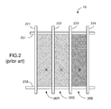
Figure 1 . As shown, thedisplay panel 1 has a plurality ofpixels 10 arranged in rows and columns in adisplay area 100 driven by adata driver 200 and agate driver 300. Thedata driver 200 is used to provide signals indicative of data on a data line to each of the columns and agate driver 300 is used to provide a gate line signal to each of the rows. In a color OLED display panel, an image is generally presented in three colors: red (R), green (G) and blue (B). Each of thepixels 10 is typically divided into three color sub-pixels:red sub-pixel 20R,green sub-pixel 20G andblue sub-pixel 20B, as shown inFigure 2 . Adata line 221 is used to provide the data signal to the R sub-pixel in a column, adata line 222 is used to provide the data signal to the G sub-pixel in the same pixel column, and adata line 223 is used to provide the data signal to the B sub-pixel in the same pixel column. Thedata line 224 is used to provide the data signal to the R sub-pixel in the next pixel column. Agate line 231 is used to provide the gate line signal to all sub-pixels in a row and agate line 232 is used to provide the gate line signal to all sub-pixels in the next row. - The present invention provides a method and a pixel driving circuit in which two or more current paths through a plurality of switching elements are used to provide the necessary current to one or more OLEDs in a pixel. In particular, the control end of each switching element is connected to the control end of the other switching elements. According to the present invention, the gate terminal of one switching element is connected to the gate terminal of another switching element, whereas each switching element is connected to a different power source line. According to various embodiments of the present invention, the different source lines are separately connected to different power sources so that the current in each current path can be separately adjustable.
- Thus, the first aspect of the present invention is a light-emitting display panel. The display panel comprises:
- a plurality of pixels arranged in a plurality of rows and columns;
- a plurality of data lines, each data line arranged to provide data signals to the pixels in a column;
- a plurality of gate lines, each gate line arranged to provide scan signals to the pixels in a row, wherein each pixel comprises:
- a control switching element having a first switching end arranged to receive data signals from a data line, a second switching end, and a control end arranged to receive a scan signal;
- a first switching element comprising:
- a first switching terminal arranged to receive electrical power for providing a first current in a first current path; a second switching terminal connected to a light-emitting component; and a control terminal connected to the second switching end of the control switching element; and
- a second switching element comprising: a first switching terminal arranged to receive electrical power for providing a second current in a second current path; a second switching terminal connected to the light-emitting component; and a control terminal connected to the second switching end of the control switching element.
- According to some embodiments, the light-emitting component comprises: a first light-emitting diode arranged to receive the first current from the first current path; anda second light-emitting diode arranged to receive the second current from the second current path.
- According to various embodiments of the present invention, each pixel comprises:
- a first capacitor connected between the first switching terminal and the control terminal of the first switching element, and a second capacitor connected between the switching terminal and the control terminal of the second switching element.
- The first switching element is arranged to receive electrical power from a first power source and the second switching element is arranged to receive electrical power from a different second power source.
- According to one embodiment of the present invention, each pixel comprises a pixel length, wherein the first switching element and the first light-emitting diode are located at a first end of the pixel length, and the second switching element and the second light-emitting diode are located at a second end of the pixel length. Each pixel is adjacent to a first power source line and a second power line along the pixel length, the first switching element arranged to receive electrical power from a first power source line and the second switching element arranged to receive electrical power from a second power source line.
- The second aspect of the present invention is a method for use in a light-emitting display panel, the light-emitting display panel comprising:
- a plurality of pixels arranged in a plurality of rows and columns;
- a plurality of data lines, each data line arranged to provide data signals to the pixels in a column;
- a plurality of gate lines, each gate line arranged to provide scan signals to the pixels in a row, wherein each pixel comprises a light-emitting component, wherein each of the pixels comprises a control switching element having a first switching end arranged to receive data signals from a data line, a second switching end, and a control end arranged to receive a scan signal, and each of the pixels comprises a light emitting component, said method comprising:
- disposing a first current path in said each of the pixels for providing a first current to the light emitting component, and
- disposing a different second current path in said each of the pixels for providing a second current to the light emitting component,
- controlling the first current in the first current path through a first switching element, and
- controlling the second current in the second current path through a second switching element, the first switching element comprising:
- a first switching terminal arranged to receive electrical power for providing the first current in the first current path, a second switching terminal connected to the light-emitting component, and a control terminal connected to the second switching end of the control switching element; and
- the second switching element comprising: a first switching terminal arranged to receive electrical power for providing the second current in the second current path, a second switching terminal connected to the light-emitting component, and a control terminal connected to the second switching end of the control switching element.
- According to various embodiments of the present invention, the light-emitting component comprises: a first light-emitting diode arranged to receive the first current from the first current path; and a second light-emitting diode arranged to receive the second current from the second current path. Each pixel comprises a pixel length, wherein the first switching element and the first light-emitting diode are located at a first end of the pixel length, and the second switching element and the second light-emitting diode are located at a second end of the pixel length.
- The present invention will become apparent upon reading the description taken in conjunction with
Figures 3 to 11 . -
-
Figure 1 shows a typical OLED display panel. -
Figure 2 shows three color sub-pixels in a pixel in a typical OLED display panel. -
Figure 3 shows a portion of the display area having a plurality of pixels, according to various embodiments of the present invention. -
Figure 4 shows a pixel and its driving circuit, according to one embodiment of the present invention. -
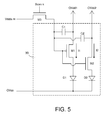
Figure 5 shows a pixel and its driving circuit, according to another embodiment of the present invention. -
Figure 6 shows a pixel and its driving circuit, according to yet another embodiment of the present invention. -
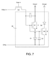
Figure 7 shows a pixel and its driving circuit, according to still another embodiment of the present invention. -
Figure 8 shows a pixel and its driving circuit, according to a different embodiment of the present invention. -
Figure 9 shows a pixel and its driving circuit, according to yet another embodiment of the present invention. -
Figure 10 shows an exemplary layout of a pixel, according to the present invention. -
Figure 11 shows another layout of a pixel, according to the present invention. - In a typical OLED display panel, a power source is used to provide a voltage to a plurality of pixels. A conductor is used to provide the voltage to each of the pixels as a drain voltage applied to a TFT which regulates the current through a connecting OLED. The conductor inherently has a resistance, causing a drop in the voltage in proportion to the current. The voltage drop can be substantial if the current is high. As a result, the brightness of the display may vary noticeably among the pixels, affecting the viewing quality of an OLED display panel.
- The present invention provides a pixel driving circuit and a method for improving the viewing quality of the OLED display panel by reducing the voltage drop in the pixels. According to various embodiments of the present invention, the drain voltage applied to the switching elements in the OLED pixels comprises two or more separate lines OVdd1, OVdd2. If the source voltage line in each pixel is short, it is sufficient to use only one source voltage line OVss. For example, if the OLED is fabricated on a substrate where one end of the diode is in direct contact with an electrically conducting plane, the voltage drop on the OVss side is negligible. However, it is also possible to use two or more OVss lines. As shown in
Figure 3 , eachpixel 22 has apixel area 30 and eachpixel area 30 has two separate conductors connected to OVdd1 and OVdd2. Gn, Gn+1, ... are gate lines for providing gate line data and Dm, Dm+1, ... are data lines for providing data signal. - In one embodiment of the present invention, a
pixel area 30 comprises two OLEDs, D1 and D2, separately connected to two TFFs, M1 and M2 to form two separate current paths (shown with current I1 and current I2). The gate terminals of M1 and M2 are connected together such that, in effect, the current paths are connected in parallel. Both M1 and M2 are p-type TFFs arranged to be switched on or off simultaneously by a switching element M3, which can be a TFT. One end of the TFT M3 is connected to a data line to receive a signal Vdata m and the gate terminal of M3 is connected to a gate line to receive a scan signal n. Each of the current 11 and current I2 has a storage capacitor C1, C2 connected to the switching element M3. - With two or more OLEDs in each OLED pixel, it is possible to reduce the current I1 and current I2 to achieve the brightness from one OLED with a higher current. As a result, the voltage drop in each of the current paths is smaller than the voltage drop if only one current path is used to produce light. For example, the current used in only one current path to produce light at a certain brightness level is I, then it is possible to use I1<I and I2<I to achieve the same brightness level. If the brightness of an OLED is proportional to the current, then I=I1 + 12.
- In another embodiment of the present invention, one of the current regulating TFTs is a p-type TFT and the other is an n-type TFT as shown in
Figure 5 . - In yet another embodiment of the present invention, both M1 and M2 are n-type TFFs.
- In the embodiments as shown in
Figures 4 to 6 , it is possible to put the anodes of both M1 and M2 in contact with an electrically conducting layer on a substrate where OVss is provided. As such, the voltage drop on the OVss side is substantially eliminated. - In a current path wherein an n-type TFT is used to regulate the current through the OLED, it is also possible to connect one switching end of the TFT to OVss, as shown in
Figures 7 and8 . In this configuration, it would be advantageous to keep the connector between the source terminal of the TFT or TFTs to the OVss source very short so as to reduce the voltage drop on the OVss side. - It should be noted that, according to various embodiments of the present invention, the voltage drop on OVdd can be reduced by using two or more current paths to provide the current to an OLED on each of the current paths. It is possible to achieve a similar voltage-drop reduction by passing the currents from two or more current paths to one OLED, as shown in
Figure 9 . - In summary, the present invention provides a method and a pixel driving circuit in which two or more current paths, through a plurality of switching elements, are used to provide the necessary current to one or more OLEDs in a pixel. In particular, the control end of each switching element is connected to the control end of the other switching elements. For example, as shown in
Figures 4 to 6 , the gate terminal of TFT M1 is connected to the gate terminal of TFT M2. According to various embodiments of the present invention, each switching element has a separate power source OVdd so that the power sources can be separately adjustable. Furthermore, with separate power sources, it is possible to arrange OVdd1 and OVdd2 to be provided from different directions. For example, each of thepixels 30 as shown inFigure 4 represents a color sub-pixel R, B or G. The color sub-pixels can be arranged side-by-side, with two power-source lines OVdd1, OVdd2 located between two adjacent color sub-pixels such as B and G. In each of the sub-pixels R, B and G, the TFT M1 is located at one end of the sub-pixel and the other TFT M2 is located at the other end. As shown inFigure 10 , the sub-pixel 30 has a width separated by a data line (Vdata) and one of power-source lines OVdd1 and OVdd2, and a length separated by a scan line and a source-supply line OVDD. Along the length the sub-pixel has a first end a second end. The first end has afirst OLED area 32 and the second end has asecond OLED area 34. At the first end, TFT M1 is used to provide the current path to OLED D1 in thefirst OLED area 32. At the second end, TFT M2 is used to provide the current path to OLED D2 in thesecond OLED area 34. As such, the power-source line OVdd1 provides a source voltage to TFT M1 from the first end and the power-source line OVdd2 provides a source voltage to TFT M2 from the second end. Since each TFT is connected to a separate power-source line at a short distance, the voltage drop of OVdd1 and OVdd2 can be reduced. - In other embodiments, the power sources that provide electrical power to M1 and M2 are connected to the same power source OVDD, as shown in
Figure 11 . Thus, the power source lines OVdd1 and OVd2 as shown inFigure 10 can be combined into a power source line OVdd. - Thus, although the present invention has been described with respect to one or more embodiments thereof, it will be understood by those skilled in the art that the foregoing and various other changes, omissions and deviations in the form and detail thereof may be made without departing from the scope of this invention.
Claims (14)
- A light-emitting display panel, comprising:a plurality of pixels arranged in a plurality of rows and columns;a plurality of data lines, each data line arranged to provide data signals to the pixels in a column;a plurality of gate lines, each gate line arranged to provide scan signals to the pixels in a row, wherein each pixel comprises:a control switching element having a first switching end arranged to receive data signals from a data line, a second switching end, and a control end arranged to receive a scan signal;a first switching element comprising:a first switching terminal arranged to receive electrical power for providing a first current in a first current path;a second switching terminal connected to a light-emitting component; anda control terminal connected to the second switching end of the control switching element; anda second switching element comprising:a first switching terminal arranged to receive electrical power for providing a second current in a second current path;a second switching terminal connected to the light-emitting component; anda control terminal connected to the second switching end of the control switching element.
- The display panel of claim 1, wherein the light-emitting component comprises:a first light-emitting diode arranged to receive the first current from the first current path;
anda second light-emitting diode arranged to receive the second current from the second current path. - The display panel of claim 1, wherein each of the first switching element and the second switching element comprises a p-type transistor.
- The display panel of claim 1, wherein each of the first switching element and the second switching element comprises an n-type transistor.
- The display panel of claim 1, wherein the first switching element comprises a p-type transistor and the second switching element comprises an n-type transistor.
- The display panel of claim 1, wherein each pixel further comprises:a capacitor connected between the first switching terminal and the control terminal of the first switching element.
- The display panel of claim 1, wherein the first switching element is arranged to receive electrical power from a first power source and the second switching element is arranged to receive electrical power from a different second power source.
- The display panel of claim 2, wherein each pixel comprises a pixel length, wherein the first switching element and the first light-emitting diode are located at a first end of the pixel length, and the second switching element and the second light-emitting diode are located at a second end of the pixel length.
- The display panel of claim 8, wherein each pixel is adjacent to a first power source line and a second power source line along the pixel length, the first switching element arranged to receive electrical power from the first power source line and the second switching element arranged to receive electrical power from the second power source line.
- The display panel of claim 1, wherein each pixel comprises a color sub-pixel.
- A method for use in a light-emitting display panel, the light-emitting display panel comprising:a plurality of pixels arranged in a plurality of rows and columns;a plurality of data lines, each data line arranged to provide data signals to the pixels in a column;a plurality of gate lines, each gate line arranged to provide scan signals to the pixels in a row, wherein each pixel comprises a light-emitting component, wherein each of the pixels comprises a control switching element having a first switching end arranged to receive data signals from a data line, a second switching end, and a control end arranged to receive a scan signal, and each of the pixels comprises a light emitting component, said method comprising:disposing a first current path in said each of the pixels for providing a first current to the light emitting component, anddisposing a different second current path in said each of the pixels for providing a second current to the light emitting component,controlling the first current in the first current path through a first switching element, andcontrolling the second current in the second current path through a second switching element, the first switching element comprising:a first switching terminal arranged to receive electrical power for providing the first current in the first current path;a second switching terminal connected to the light-emitting component; anda control terminal connected to the second switching end of the control switching element; andthe second switching element comprising:a first switching terminal arranged to receive electrical power for providing the second current in the second current path;a second switching terminal connected to the light-emitting component; anda control terminal connected to the second switching end of the control switching element.
- The method of claim 11, wherein the light-emitting component comprises:a first light-emitting diode arranged to receive the first current from the first current path; anda second light-emitting diode arranged to receive the second current from the second current path.
- The method of claim 12, wherein each pixel comprises a pixel length, wherein the first switching element and the first light-emitting diode are located at a first end of the pixel length, and the second switching element and the second light-emitting diode are located at a second end of the pixel length.
- The method of claim 13, further comprising:arranging a first power source line and a second power line along the pixel length such that each pixel is adjacent to both the first power source line and the second power source line;arranging the first switching element for receiving electrical power from the first power source line and the second switching element for receiving electrical power from the second power source line.
Applications Claiming Priority (1)
| Application Number | Priority Date | Filing Date | Title |
|---|---|---|---|
| US12/584,221 US8692742B2 (en) | 2009-09-01 | 2009-09-01 | Pixel driving circuit with multiple current paths in a light emitting display panel |
Publications (1)
| Publication Number | Publication Date |
|---|---|
| EP2293275A1 true EP2293275A1 (en) | 2011-03-09 |
Family
ID=42077263
Family Applications (1)
| Application Number | Title | Priority Date | Filing Date |
|---|---|---|---|
| EP09180882A Ceased EP2293275A1 (en) | 2009-09-01 | 2009-12-29 | Pixel driving circuit for light emitting display panel |
Country Status (4)
| Country | Link |
|---|---|
| US (1) | US8692742B2 (en) |
| EP (1) | EP2293275A1 (en) |
| CN (1) | CN101833916B (en) |
| TW (1) | TWI415072B (en) |
Cited By (1)
| Publication number | Priority date | Publication date | Assignee | Title |
|---|---|---|---|---|
| US11670900B2 (en) | 2019-02-05 | 2023-06-06 | Emergency Technology, Inc. | Universal smart adaptor |
Families Citing this family (24)
| Publication number | Priority date | Publication date | Assignee | Title |
|---|---|---|---|---|
| TWI404447B (en) * | 2009-12-28 | 2013-08-01 | Au Optronics Corp | Pixel structure of electroluminescent display panel |
| WO2011145174A1 (en) * | 2010-05-18 | 2011-11-24 | キヤノン株式会社 | Display device |
| JP2012109137A (en) * | 2010-11-18 | 2012-06-07 | Canon Inc | Organic el display device |
| JP2013008663A (en) * | 2011-05-24 | 2013-01-10 | Canon Inc | Display device |
| CN102891164B (en) * | 2011-07-19 | 2016-09-07 | 群创光电股份有限公司 | Organic Electroluminescence Display Device |
| KR101902500B1 (en) * | 2012-04-16 | 2018-10-01 | 삼성디스플레이 주식회사 | Organic light emitting diode display |
| US9257665B2 (en) * | 2012-09-14 | 2016-02-09 | Universal Display Corporation | Lifetime OLED display |
| BR112015021790A2 (en) * | 2013-03-11 | 2017-07-18 | Koninklijke Philips Nv | auto stereoscopic screen |
| KR102047003B1 (en) * | 2013-04-24 | 2019-11-21 | 삼성디스플레이 주식회사 | Organic Light Emitting Display |
| KR102042192B1 (en) * | 2013-04-30 | 2019-11-08 | 삼성디스플레이 주식회사 | Pixel and Organic Light Emitting Display Device Using the same |
| TWI478128B (en) * | 2013-05-23 | 2015-03-21 | Au Optronics Corp | LED display panel |
| TWI534993B (en) * | 2013-09-25 | 2016-05-21 | 友達光電股份有限公司 | Pixel structure of inorganic light-emitting diode |
| TWI467528B (en) * | 2013-10-30 | 2015-01-01 | 友達光電股份有限公司 | Light-emitting diode display panel and manufacturing method thereof |
| CN103531149B (en) * | 2013-10-31 | 2015-07-15 | 京东方科技集团股份有限公司 | AC (alternating current)-driven pixel circuit, driving method and display device |
| CN104050915B (en) * | 2014-05-30 | 2015-06-03 | 京东方科技集团股份有限公司 | AMOLED display panel and AMOLED display device |
| CN104751801B (en) * | 2015-04-17 | 2018-09-04 | 京东方科技集团股份有限公司 | Pixel-driving circuit and its driving method and display device |
| CN109727531A (en) * | 2017-10-31 | 2019-05-07 | 云谷(固安)科技有限公司 | A kind of display panel and terminal |
| DE102018114175A1 (en) | 2018-06-13 | 2019-12-19 | Osram Opto Semiconductors Gmbh | Arrangement for a display and method |
| TWI680445B (en) * | 2018-11-16 | 2019-12-21 | 友達光電股份有限公司 | Driving circuit |
| CN110634441A (en) * | 2019-08-28 | 2019-12-31 | 武汉华星光电半导体显示技术有限公司 | OLED display panel |
| CN113450698B (en) * | 2020-06-23 | 2022-05-31 | 重庆康佳光电技术研究院有限公司 | Display device, sub-pixel repair circuit and repair method thereof |
| WO2021258283A1 (en) | 2020-06-23 | 2021-12-30 | 重庆康佳光电技术研究院有限公司 | Display device, sub-pixel repair circuit and repair method therefor |
| US20240215359A1 (en) * | 2021-04-08 | 2024-06-27 | Semiconductor Energy Laboratory Co., Ltd. | Display device, electronic device, and method for manufacturing display device |
| CN115100988B (en) * | 2022-06-22 | 2025-06-24 | 合肥维信诺科技有限公司 | Array substrate, display panel and display device |
Citations (10)
| Publication number | Priority date | Publication date | Assignee | Title |
|---|---|---|---|---|
| US20010043168A1 (en) | 2000-05-12 | 2001-11-22 | Semiconductor Energy Laboratory Co., Ltd. | Display device |
| EP1193741A2 (en) | 2000-09-29 | 2002-04-03 | SANYO ELECTRIC Co., Ltd. | Semiconductor device having thin film transistor for supplying current to driven element |
| US6522079B1 (en) | 1999-10-01 | 2003-02-18 | Sanyo Electric Co., Ltd. | Electroluminescence display device |
| US20040004443A1 (en) | 2002-07-08 | 2004-01-08 | Park Jae Yong | Organic electro luminescence device and method for driving the same |
| US20040227707A1 (en) | 2000-04-27 | 2004-11-18 | Semiconductor Energy Laboratory Co., Ltd. | Light emitting device |
| US20050237279A1 (en) * | 2004-04-21 | 2005-10-27 | Wen-Kuen Chen | Bottom and top emission OLED pixel structure |
| US20060061525A1 (en) * | 2004-09-21 | 2006-03-23 | Kim Eun-Ah | Organic electroluminescent display device having plurality of driving transistors and plurality of anodes or cathodes per pixel |
| US20070008269A1 (en) | 2000-04-26 | 2007-01-11 | Semiconductor Energy Laboratory Co., Ltd. | Electronic device and driving method thereof |
| US20070182671A1 (en) * | 2003-09-23 | 2007-08-09 | Arokia Nathan | Pixel driver circuit |
| US20090166638A1 (en) * | 2007-12-27 | 2009-07-02 | Semiconductor Energy Laboratory Co., Ltd. | Display device and electronic device provided with the same |
Family Cites Families (9)
| Publication number | Priority date | Publication date | Assignee | Title |
|---|---|---|---|---|
| US20050030268A1 (en) | 2002-08-27 | 2005-02-10 | Weixiao Zhang | Full-color electronic device with separate power supply lines |
| US7528810B2 (en) | 2004-05-25 | 2009-05-05 | Victor Company Of Japan, Limited | Display with multiple emission layers |
| KR100570774B1 (en) * | 2004-08-20 | 2006-04-12 | 삼성에스디아이 주식회사 | Memory management method for display data of light emitting display device |
| US7105855B2 (en) | 2004-09-20 | 2006-09-12 | Eastman Kodak Company | Providing driving current arrangement for OLED device |
| KR100592636B1 (en) | 2004-10-08 | 2006-06-26 | 삼성에스디아이 주식회사 | LED display device |
| KR100624126B1 (en) * | 2005-04-27 | 2006-09-19 | 삼성에스디아이 주식회사 | Organic light emitting display device and manufacturing method |
| KR101251375B1 (en) * | 2005-12-30 | 2013-04-05 | 엘지디스플레이 주식회사 | Dual panel type organic electro-luminescent device |
| CN101373576B (en) * | 2007-08-24 | 2012-05-09 | 奇美电子股份有限公司 | Image display system |
| JP5086766B2 (en) | 2007-10-18 | 2012-11-28 | グローバル・オーエルイーディー・テクノロジー・リミテッド・ライアビリティ・カンパニー | Display device |
-
2009
- 2009-09-01 US US12/584,221 patent/US8692742B2/en active Active
- 2009-12-29 EP EP09180882A patent/EP2293275A1/en not_active Ceased
- 2009-12-31 TW TW098146491A patent/TWI415072B/en active
-
2010
- 2010-01-25 CN CN2010101053953A patent/CN101833916B/en active Active
Patent Citations (10)
| Publication number | Priority date | Publication date | Assignee | Title |
|---|---|---|---|---|
| US6522079B1 (en) | 1999-10-01 | 2003-02-18 | Sanyo Electric Co., Ltd. | Electroluminescence display device |
| US20070008269A1 (en) | 2000-04-26 | 2007-01-11 | Semiconductor Energy Laboratory Co., Ltd. | Electronic device and driving method thereof |
| US20040227707A1 (en) | 2000-04-27 | 2004-11-18 | Semiconductor Energy Laboratory Co., Ltd. | Light emitting device |
| US20010043168A1 (en) | 2000-05-12 | 2001-11-22 | Semiconductor Energy Laboratory Co., Ltd. | Display device |
| EP1193741A2 (en) | 2000-09-29 | 2002-04-03 | SANYO ELECTRIC Co., Ltd. | Semiconductor device having thin film transistor for supplying current to driven element |
| US20040004443A1 (en) | 2002-07-08 | 2004-01-08 | Park Jae Yong | Organic electro luminescence device and method for driving the same |
| US20070182671A1 (en) * | 2003-09-23 | 2007-08-09 | Arokia Nathan | Pixel driver circuit |
| US20050237279A1 (en) * | 2004-04-21 | 2005-10-27 | Wen-Kuen Chen | Bottom and top emission OLED pixel structure |
| US20060061525A1 (en) * | 2004-09-21 | 2006-03-23 | Kim Eun-Ah | Organic electroluminescent display device having plurality of driving transistors and plurality of anodes or cathodes per pixel |
| US20090166638A1 (en) * | 2007-12-27 | 2009-07-02 | Semiconductor Energy Laboratory Co., Ltd. | Display device and electronic device provided with the same |
Cited By (2)
| Publication number | Priority date | Publication date | Assignee | Title |
|---|---|---|---|---|
| US11670900B2 (en) | 2019-02-05 | 2023-06-06 | Emergency Technology, Inc. | Universal smart adaptor |
| US12444894B2 (en) | 2019-02-05 | 2025-10-14 | Emergency Technology, Inc. | Smart adaptor assembly |
Also Published As
| Publication number | Publication date |
|---|---|
| US8692742B2 (en) | 2014-04-08 |
| CN101833916A (en) | 2010-09-15 |
| CN101833916B (en) | 2013-06-12 |
| US20110050550A1 (en) | 2011-03-03 |
| TW201110089A (en) | 2011-03-16 |
| TWI415072B (en) | 2013-11-11 |
Similar Documents
| Publication | Publication Date | Title |
|---|---|---|
| US8692742B2 (en) | Pixel driving circuit with multiple current paths in a light emitting display panel | |
| US10356858B2 (en) | MicroLED display panel | |
| US8896505B2 (en) | Display with pixel arrangement | |
| CN113383382A (en) | Array substrate, display panel, spliced display panel and display driving method | |
| US11942032B2 (en) | Display apparatus including power line comprising first power line in first direction and second power line in second direction | |
| JP3977299B2 (en) | Electro-optical device, matrix substrate, and electronic apparatus | |
| US20090262046A1 (en) | High aperture ratio pixel layout for display device | |
| US10621912B2 (en) | Display device to display images on rear and front surfaces independently of each other | |
| US11088235B2 (en) | Display panel and display device for improving display effect | |
| CN119866145A (en) | Display panel and display device | |
| US11217158B2 (en) | Pixel structure and display panel | |
| KR102550859B1 (en) | Light emitting device, display panel and display device | |
| US20080204377A1 (en) | Organic EL display device | |
| CN115104186B (en) | Display substrate, display panel and display device | |
| EP3929904A1 (en) | Display device | |
| US20110291098A1 (en) | Organic el display device, mother substrate of organic el display device, and method of testing organic el display device | |
| KR20230019898A (en) | Organic light emitting display device | |
| US7570277B2 (en) | Electroluminescence display device | |
| KR20170081030A (en) | Organic light emitting display panel and organic light emitting display device | |
| JP4944547B2 (en) | Image display device and manufacturing method or driving method thereof | |
| TWI906951B (en) | Display device | |
| US20250160150A1 (en) | Display device | |
| US20210304674A1 (en) | Optoelectronic emitting device and method for controlling an optoelectronic emitting device |
Legal Events
| Date | Code | Title | Description |
|---|---|---|---|
| PUAI | Public reference made under article 153(3) epc to a published international application that has entered the european phase |
Free format text: ORIGINAL CODE: 0009012 |
|
| 17P | Request for examination filed |
Effective date: 20100129 |
|
| AK | Designated contracting states |
Kind code of ref document: A1 Designated state(s): AT BE BG CH CY CZ DE DK EE ES FI FR GB GR HR HU IE IS IT LI LT LU LV MC MK MT NL NO PL PT RO SE SI SK SM TR |
|
| AX | Request for extension of the european patent |
Extension state: AL BA RS |
|
| 17Q | First examination report despatched |
Effective date: 20110418 |
|
| STAA | Information on the status of an ep patent application or granted ep patent |
Free format text: STATUS: THE APPLICATION HAS BEEN REFUSED |
|
| 18R | Application refused |
Effective date: 20140630 |