EP2290860B1 - A pluggable conversion module for a data transport card of a wavelength division multiplexing system - Google Patents
A pluggable conversion module for a data transport card of a wavelength division multiplexing system Download PDFInfo
- Publication number
- EP2290860B1 EP2290860B1 EP09167376.4A EP09167376A EP2290860B1 EP 2290860 B1 EP2290860 B1 EP 2290860B1 EP 09167376 A EP09167376 A EP 09167376A EP 2290860 B1 EP2290860 B1 EP 2290860B1
- Authority
- EP
- European Patent Office
- Prior art keywords
- wdm
- data
- optical
- transport card
- data transport
- Prior art date
- Legal status (The legal status is an assumption and is not a legal conclusion. Google has not performed a legal analysis and makes no representation as to the accuracy of the status listed.)
- Active
Links
Images


Classifications
-
- H—ELECTRICITY
- H04—ELECTRIC COMMUNICATION TECHNIQUE
- H04J—MULTIPLEX COMMUNICATION
- H04J14/00—Optical multiplex systems
- H04J14/02—Wavelength-division multiplex systems
Definitions
- the invention relates to a pluggable module for a data transport card of a wavelength division multiplexing system and a corresponding method for transporting data via an optical fibre.
- wavelength division multiplexing In a wavelength division multiplexing (WDM) system multiple optical carrier signals are multiplexed on a single optical fibre by using different wavelengths or colors of laser light to carry different optical signals.
- the wavelength division multiplexing technology uses efficiently the capacity of an optical fibre and enables a bidirectional communication over one optical fibre.
- the wavelength division multiplex (WDM) systems allow to expand the capacity of the network without laying additional fibres. WDM systems can operate on single mode fibre optical cables.
- Wavelength division multiplexing (WDM) systems can comprise coarse and dense wavelength division multiplexing (WDM) systems.
- Optical fibres can be used to transmit optical data signals to transport information data from at least one source client to at least one target client.
- Each client can provide one or several high speed data streams of different formats such as Ethernet data streams, InfiniBand data streams or Fibre Channel data streams.
- PROCEEDINGS IEEE, PI, 1 April 2006 (2006-04-01), pages 1-5, ISBN: 978-1-4244-0221-2 , " Super-channel architectures for in-service capacity expansion of CWDM/DWDM systems", by R. Antonsik, TRANSPARENT OPTICAL NETWORKS, 2003. PROCEEDINGS OF 2003 5TH INTERNATIO NAL CONFERENCE ON WARSAW, POLAND 29 JUNE-3 JULY 2003, PISCATAWAY, NJ, USA,IEEE, US, vol.
- the pluggable conversion module according to the present invention as employed by a WDM system is highly flexible and allows different configurations for different applications or network environments.
- a further advantage of the pluggable conversion module according to the present invention is that it can be implemented with comparatively low costs and complexity.
- a further advantage of the pluggable conversion module according to the present invention is that it can be easily miniaturized and needs only few space when integrated in a chip.
- the pluggable conversion module according to the present invention works bidirectionally and can be used on the transmission side and on the reception side of a WDM data transport system.
- a wavelength division multiplexing (WDM) data transport system 1 can comprise several clients 2 each having at least one data transport card 3.
- a client 2 can be any kind of data processing unit such as a host computer, a router or any kind of data source or sink generating high speed data streams or processing high speed data streams.
- the data transport card 3 as shown in figure 1 can be inserted in a possible embodiment into a card slot of the respective client 2.
- the data transport card 3 receives data streams from different clients via data ports and can be integrated in a separate device.
- the data transport card 3 comprises an interface 4 to receive high speed data streams DS from one or several clients 2.
- the data streams DS are high speed data streams having a bit rate of more than 4 GBit/sec.
- the data format of the data streams DS can vary.
- the data streams DS comprise Ethernet data streams, Fibre Channel data streams or InfiniBand data streams.
- the data streams DS as shown in figure 1 can be received by the interface 4 from the same or different client 2.
- the client 2 is a 100 GBE Ethernet client for providing four data streams DS each having a bit rate of 25 GBit/sec.
- the interface 4 is a bidirectional interface and can supply data streams to the client 2 as well.
- the data transport card 3 can comprise a socket or receiving means for the plug-in of a pluggable conversion module 5 according to the present invention.
- the pluggable conversion module 5 is integrated into a housing or chip.
- the pluggable conversion module 5 of the data transport card 3 converts the data streams DS into optical data signals and couples these optical data signals into at least one wavelength division multiplexing (WDM) channel for transport of the optical data signals via an optical fibre 6 as shown in figure 1 .
- WDM wavelength division multiplexing
- the pluggable conversion module 5 works bidirectionally and also converts optical data signals received via the optical fibre 6 in different wavelength division multiplexing (WDM) subchannels of at least one wavelength division multiplexing (WDM) channel into data streams for the at least one client 2.
- WDM wavelength division multiplexing
- the pluggable conversion module 5 in the embodiment of figure 1 can be a bidirectional pluggable conversion module performing a conversion between optical data signals and data streams in both directions.
- the data transport card 3 comprises two separate pluggable conversion modules 5-1, 5-2 wherein the first pluggable conversion module 5-1 is provided for performing the conversion of the data streams into optical data signals and the other pluggable conversion module 5-2 is provided for performing the conversion of optical data signals into data streams.
- the optical fibre 6 has a broad bandwidth for transporting data.
- 40 to 80 100 GHz WDM channels can be provided by one optical fibre 6.
- the optical fibre 6 provides bandwidth for 80 to 160 50 GHz WDM channels.
- each WDM channel can comprise one or several WDM subchannels.
- each WDM channel has a bandwidth of 100 GHz and comprises four 25 GHz WDM subchannels.
- each WDM channel has a bandwidth of 100 GHz and comprises two 50 GHz WDM subchannels.
- the wavelength division multiplexing WDM channel as employed by the WDM data transport system 1 according to the present invention has a predetermined bandwidth and comprises of WDM subchannels corresponding in a preferred embodiment to a number N of data streams DS.
- the data transport card 3 comprises in the embodiment of figure 2 an electronic module 7 which is provided between the bidirectional data stream interface 4 and the pluggable conversion module 5.
- the electronic module 7 performs different functions such as deskewing, framing, monitoring, error correction of the data streams DS received from the interface 4 and supplied to the interface 4.
- the electronic module 7 can comprise different subunits such as a mapping and framing unit which maps the data streams as into ODU data frames, a monitoring unit which monitors a data integrity, a FEC unit which performs a forward error correction of the ODU data frames and a deskewing unit which performs a deskewing of the data streams DS.
- the electronic module 7 is implemented by an FPGA unit.
- the electronic module 7 performs an additional function such as bit rate adaption or stuffing of signals. In a possible embodiment, the electronic module 7 further performs a clock adaption and multiplexing/demultiplexing functions. The provision of the electronic module 7 is optional. The electronic module 7 performs deskewing, framing and FEC. For other multiple high speed data signals, the electronic module 7 can comprise a retiming function. Further, it can perform a clock adaption and framing as well as forward error correction coding FEC.
- the forward error correction unit can be switched on or off in response to a control signal.
- the deskewing unit within the electronic module 7 can be activated or deactivated by means of a control signal. Accordingly, it is possible to provide a low signal latency.
- the pluggable conversion module 5 comprises in the transmitting signal path a laser array 5A for converting the data streams DS processed by the electronic module 7 into optical data signals.
- the laser array 5A is in a possible embodiment a directly modulated laser array (DML laser array).
- the directly modulated laser array is a CML laser array.
- the laser array 5A can be formed by an externally modulated (EML) laser array.
- EML externally modulated
- the laser array 5A is tuneable.
- the laser array 5A can be tuneable in response to a feedback control signal received by the pluggable conversion module 5 as shown in figure 2 from a receive end data transport card at the far end side via an inband or outband embedded communication channel ECC.
- the inband or outband embedded communication channel ECC is provided for transporting said feedback control signal sent by said receive end transport card back to said data transport card 3 via the optical fibre 6.
- the pluggable conversion module 5 comprises further in the transmitting signal path a tuneable optical signal reshaper TOSR 5B being adaptable to the bandwidth and to the frequency spacing of the WDM subchannels to optimize WDM subchannel power levels P and to minimize crosstalk.
- the tuneable optical signal reshaper TOSR 5B is provided for spectrum shaping of the WDM subchannels wherein the WDM subchannel bandwidth and the frequency spacing of the subchannel center frequencies are adjusted to minimize a bit error rate (BER) of the optical data signals transported via the optical fibre 6.
- the tuneable optical signal reshaper TOSR 5B is also tuneable in response to a feedback control signal from the receive end data transport card sent via the inband or outband communication channel ECC.
- the tuneable optical signal reshaper TOSR 5B can be formed by a filter.
- the tuneable or adaptable optical signal reshaper TOSR 5B is tuneable with respect to both, channel bandwidth of the WDM subchannels and their periodicity or grid spacing.
- the pluggable conversion module 5 is adapted to be tuneable to a wider extent to reduce the number of module variants or spare parts.
- the laser light signals can be tuned, e.g. thermally, over a range of several WDM subchannels, for example over a range of eight WDM subchannels each having a bandwidth of 50 GHz.
- the tuneability can range over an adaptable number of WDM subchannels, for example to an increased tuning range of nine to ten 50 GHz WDM subchannels.
- Figure 14A shows a spectrum of an embodiment with a tuning range of e.g. nine WDM subchannels.
- a thermal tuning is performed.
- a 50 GHz subchannel frequency spacing on the pluggable module is provided.
- a 25 GHz subchannel frequency spacing is provided.
- Figure 14B illustrates a further possible embodiment wherein the WDM subchannels comprise a skip-seven frequency spacing.
- 32 channels can be covered with a single module.
- 40 WDM subchannels can be covered with a single conversion module. This allows to use only one or two variants or different spare parts for a 40 channel WDM system. Accordingly, the number of spare parts is significantly reduced in this embodiment.
- the pluggable module can be thermally tuned up to 10 x 50 GHz. In this case for a skip zero, i.e. all WDM subchannels lay directly beside each other, only four variants are needed.
- a skip-9 variant in greenfield deployment in which a skip-9 variant can be used an improvement can be achieved because only a single variant of spare part is necessary.
- the number of necessary spare parts can be optimized. For example, a skip zero plus skip nine with a maximal tuning capacity of 10 x 50 GHz can be provided in one embodiment. With this embodiment using skips zero plus skip seven/eight/nine the number of spare parts and/or production variants can be minimized. Five (skip 0 tuned 8 x 50 GHz upgrade) plus two (skip 7 tuned 8 x 50 GHz, greenfield) gives a total of seven production variants.
- skip 0 tuned 9 x 50 GHz, upgrade plus two (skip 8 tuned 9 x 50 GHz, Greenfield) lead to a maximum of only five production variants.
- the pluggable conversion module 5 further comprises on its receiving signal path a photodiode PD array 5D and a tuneable subchannel WDM filter TWDM 5C for each WDM channel for decoupling the WDM subchannels.
- the data transport card 3 as shown in figure 2 comprises switching means to bypass the electronic module 7.
- subunits of the electronic module 7 can be bypassed.
- FIG 3 shows a diagram of an active optical fibre 6 which can be used as a component in the WDM data transport system 1 according to the present invention.
- the active optical fibre 6 comprises a first pluggable conversion module 5-1 on the transmitting side and a second pluggable conversion module 5-2 on the receiving side.
- the pluggable conversion modules 5-1, 5-2 are bidirectional and have the structure of a pluggable conversion module 5 as shown in figure 2 .
- the active optical fibre 6 as shown in figure 3 can be plugged into a data transport card 3-1 on the transmitting side and into a data transport card 3-2 on the receiving side.
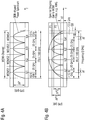
- Figures 4A, 4B show a spectrum for illustrating the functionality of a pluggable conversion module 5 of the present invention as employed in a WDM data transport system 1.
- the diagrams of figures 4A, 4B show the spectral power density SPD of four WDM subchannels within one WDM channel having a predetermined bandwidth of 100 GHz.
- the four WDM subchannels each have the bandwidth of 25 GHz wherein the center frequencies f ci of the four WDM subchannels are spaced from each other and have a frequency spacing of 25 GHz.
- Figures 4A, 4B show the four center frequencies f c1 , f c2 , f c3 , f c4 of the four WDM subchannels within the WDM channel having a bandwidth of 100 GHz.
- the optical fibre 6 may provide a bandwidth for a plurality of WDM channels each having several WDM subchannels as shown in figures 4A, 4B .
- each WDM subchannel show a ODB shaped power spectrum of an optical duo-binary (ODB) modulation format.
- ODB optical duo-binary
- the optical duo-binary ODB modulation format provides the advantage that it provides a narrow spectrum and high tolerance to chromatic dispersion.
- Other modulation formats are possible as well.
- the optical data signals comprise an amplitude modulation format or a phase modulation format.
- the WDM subchannels do not overlap.
- the WDM channel has four WDM subchannels WDMS1, WDMS2, WDMS3 and WDMS4. Since the outer two WDM subchannels WDMS1, WDMS4 suffer from external 100 GHz WDM filters of the system more than the inner WDM subchannels WDMS2, WDMS3 the pluggable conversion module 5 according to the present invention performs a spectrum shaping of the WDM subchannels such that the subchannel spacing is tuned to be less than 25 GHz as illustrated in the lower spectrum as shown in figure 4B .
- the WDM subchannel bandwidth of the WDM subchannels WDMSi and the frequency spacing of the subchannel center frequency f ci are adjusted to minimize the bit error rate BER of the transported optical data signals.
- the subchannel spacing of e.g. 25 GHz is tuned to be less than 25 GHz leading to slightly overlapping data subchannel spectra as indicated in the lower diagram of figure 4B .
- the WDM subchannels WDMS1 and WDMS4 are less affected by the external 100 GHz WDM filters of the system such reducing the bit error rate BER of the transmitted signal.
- the trade off is that the WDM subchannels slightly overlap each other leading to an increased bit error rate. Accordingly, the WDM subchannels WDMS i are adjusted to an optimum where the bit error rates BER of the transported optical data signals is minimal.
- the tuneable optical signal reshaper TOSR 5B is tuned as shown in figure 4 which requires the internal subchannel TWDM filter to be tuned respectively.
- the receive end FEC unit can also provide a feedback signal to the laser array 5A in order to set optimum WDM subchannel power levels P1, P2 as shown in the diagram of figure 4B .
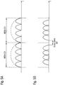
- a guard band GB is provided as shown in figure 4B which decreases the WDM filter effects. This is illustrated also in figure 5 showing the guard band GB between two WDM channels each having four WDM subchannels.
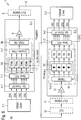
- FIG. 6 shows a possible embodiment of the WDM data transport system 1 according to the present invention.
- the WDM transport system 1 comprises one 100 Gbit/s Ethernet client 2 providing four 25 G Ethernet data streams DS to an optical client interface 4 of a data transport card 3 comprising an electronic module 7 performing inter alia deskewing and forward error correction FEC.
- the pluggable conversion module 5 is plugged into a socket of the data transport card 3 and comprises a tuneable directly modulated laser array TDML 5A for each data stream DS.
- the four 25 G Ethernet signal data streams DS are modulated after forward correction FEC.
- the DML output is combined by means of a four to one coupler or WDM multiplexer to a WDM channel.
- the optical data signals generated by the TDML laser array 5A are coupled into at least one wavelength division multiplexing WDM channel for transport of the optical data signals via the optical fibre 6.
- a single tuneable optical signal reshaper TOSR 5B is integrated into the pluggable module 5 and provides a periodic 25 GHz subcarrier grid as shown in the spectrum of figures 4A, 4B .
- An alignment of a extinction ration or adiabatic chirp is provided in order to provide an ODB modulation at the required bit rates.
- the output of the tuneable optical signal reshaper 5B can be set to a standard 100 GHz WDM grid after optional booster amplification by means of a booster amplifier 8 as shown in figure 6 .
- the optical data signals pass an ITU-DWDM 9 of the WDM system and are transmitted via the optical fibre 6 to a static dispersion compensator DCF 10 and an ITU-T-DWDM 11 at the receiving side.
- the data transport card 3-2 at the receiving end can comprise a preamplifier 12 for amplitude amplification of the received optical data signals.
- the data transport card 3-2 further comprises a socket for plugging in a pluggable conversion module 5-2 having in the shown embodiment a TWDM tuneable WDM filter 5C and a photodiode array 5D for converting the decoupled WDM subchannels into data streams DS processed by receivers RX as shown in figure 6 .
- the receive end data transport card 3-2 also comprises an electronic module 7-2 and an optical client interface 4-2 for supplying four 25 GBit/sec data streams to a 100 GBE Ethernet client 2-2.
- the functions of the electronic module 7 can be adapted by one or several control signals CRTL activating or deactivating different subunits and adjusting parameters of said subunits.
- Figure 7 shows a further embodiment of a WDM data transport system 1 according to the present invention wherein a 100 GBE client supplies 2-1 100 GbE SR 10 I/F data streams to the interface 4-1 of the data transport card 3-1 on the transmitting side.
- the tuneable optical signal reshaper 5B is formed by two 3 dB power couplers connected on the output side to a 25 G interleaving unit.
- the two 3 dB power couplers can be formed by interleaving units as well. The provision of cascaded interleaving units reduces further the bit error rate BER of the transmitted optical data signals.
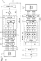
- FIG. 8 shows a further possible embodiment of a WDM data transport system 1 according to the present invention.
- four separate clients 2A-1, 2B-1, 2C-1, 2D-1 are provided on the transmitting side each generating a 16 G or a 20 G data stream DS applied to the data stream interface 4-1 of the data transport card 3-1 on the transmitting side.
- the output signal of the booster amplifier 8 is provided to a WDM demultiplexer 13 provided on the data transport card 3-1.
- the data transport card 3-2 on the receiving side comprises a corresponding WDM multiplexer 14.
- the output data streams are supplied to four separate clients 2A-2 to 2D-4.
- FIG 9 shows a further embodiment of a WDM data transport system 1 according to the present invention having a data transport card 3-1 on the transmitting side for receiving a pluggable conversion module 5-1 having four tuneable optical signal reshapers TOSR and wavelength lockers WL for each data stream DS.
- the wavelength lockers WL as shown in the different embodiments are provided for locking the WDM subchannel frequencies.
- Figure 10 shows a further exemplary embodiment of a WDM data transport system 1 according to the present invention having four separate clients 2A-1, 2B-1, 2C-1, 2D-1 on the transmitting and receiving side 2A-2, 2B-2, 2C-2, 2D-2 each generating or receiving a 16 G or 20 G data stream.
- the pluggable module 5-1 on the transmitting side comprises a single tuneable optical signal reshaper TOSR 5B.
- the TWDM 5D of the pluggable module 5-2 on the receiving side can be thermically tuned.
- FIG 11 shows a further exemplary embodiment of a WDM data transport system 1 according to the present invention.
- the has embodiment shows a client having a QSFP (Quadruple Signal Form Factor Pluggable) providing 40 GBs Infiniband data stream to a QSFP interface 4-1 of a data transport card 3-1.
- the electronic module 7-1 is formed by an FPGA unit as shown in figure 11 .
- the arrangement as shown in figure 11 can support IBQDR x 4 or 4 x 10 G or 40 GBE data streams.
- the arrangement can be extended to QDR x 12 data streams.
- Figure 12 shows a flowchart of a possible embodiment of a method for transporting data via an optical fibre 6.
- a first step S1 high speed data streams DS are received via an interface 4 from at least one or several clients 2.
- the received data streams DS are converted into optical data signals and coupled into at least one wavelength division multiplexing channel WDM having several WDM subchannels WDMS for transporting said optical data signals via the optical fibre 6.
- the optical data signals received via the optical fibre 6 in different wavelength division multiplexing subchannels WDMS of at least one wavelength division multiplexing channel WDMS which has for example a predetermined bandwidth of 100 GHz, are decoupled to data streams for at least one receiving client 2.
- step S4 the decoupled data streams are supplied to the clients 2 on the receiving side.
- the method for data transport as shown in the flowchart of figure 12 is performed on the basis of a hardware platform in real time.
- the method is performed by a computer program comprising a instructions for performing the method as shown in figure 12 .
- this computer program is loaded from a data carrier storing said computer program.
- the WDM data transport system 1 according to the present invention as shown in the different embodiments is configurable depending on the length of the optical fibre 6, in particular, the laser array 5A and the tuneable optical signal reshaper TOSR 5B can be configured to meet the different requirements of different network , environments.
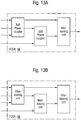
- Figures 13A, 13B show two embodiments for implementing a tuneable optical signal reshaper 5B as employed by the WDM data transport system 1 according to the present invention.
- the tuneable optical signal reshaper 5B as shown in figures 13A, 13B is formed by a separate device or by a separate pluggable module which can be plugged into the motherboard of the data transport card 3-1.
- the invention provides a flexible 100 GBE data transport system for one or multiple high speed data signals over an optical fibre 6.
- the WDM data transport system 1 according to the present invention provides different configurations supporting different environments and requirements with a relatively low complexity.
- the WDM data transport system 1 according to the present invention can be used for a wide range of different data stream formats such as Ethernet Fibre Channel or InfiniBand. Furthermore, it can be used for different kinds of optical signal modulation formats. By activating or deactivating subunits of the electronic module 7, it is possible to provide low latency variants.
- the laser array 5A is tuneable whereas in other embodiments the laser array 5A is not tuneable. If the laser array 5-1 is tuneable, it is in a preferred embodiment tuned in response to a feedback control signal sent back from the receiving side via an embedded communication channel ECC. In a possible embodiment, another data transport channel is used for sending the feedback control signal to the tuneable laser array 5A.
Description
- The invention relates to a pluggable module for a data transport card of a wavelength division multiplexing system and a corresponding method for transporting data via an optical fibre.
- In a wavelength division multiplexing (WDM) system multiple optical carrier signals are multiplexed on a single optical fibre by using different wavelengths or colors of laser light to carry different optical signals. The wavelength division multiplexing technology uses efficiently the capacity of an optical fibre and enables a bidirectional communication over one optical fibre. The wavelength division multiplex (WDM) systems allow to expand the capacity of the network without laying additional fibres. WDM systems can operate on single mode fibre optical cables.
- Wavelength division multiplexing (WDM) systems can comprise coarse and dense wavelength division multiplexing (WDM) systems. Optical fibres can be used to transmit optical data signals to transport information data from at least one source client to at least one target client. Each client can provide one or several high speed data streams of different formats such as Ethernet data streams, InfiniBand data streams or Fibre Channel data streams.
- The following prior art documents relate to the implementation of data transport cards, particularly for WDM transmission,
US2008/292322 A1 , "100GbE-Optical LAN Technologies [Applications&Practice]", by C. Cole et al, IEEE COMMUNICATIONS MAGAZINE, IEEE SERVICE CENTER, PISCATAWAY, US, vol. 45, no. 12, 1 December 2007 (2007-12-01), pages 12-19, ISSN: 0163-6804, "100 Gigabit Ethernet - Applications, Features, Challenges", by M. Duelk et al, INFOCOM 2006. 25TH IEEE INTERNATIONAL CONFERENCE ON COMPUTER COMMUNICA TIONS. PROCEEDINGS, IEEE, PI, 1 April 2006 (2006-04-01), pages 1-5, ISBN: 978-1-4244-0221-2, "Super-channel architectures for in-service capacity expansion of CWDM/DWDM systems", by R. Antonsik, TRANSPARENT OPTICAL NETWORKS, 2003. PROCEEDINGS OF 2003 5TH INTERNATIO NAL CONFERENCE ON WARSAW, POLAND 29 JUNE-3 JULY 2003, PISCATAWAY, NJ, USA,IEEE, US, vol. 2, 29 June 2003 (2003-06-29), pages 84-86, ISBN: 978-0-7803-7816-2,US 2008/069570 A1 ,US 2008/050074 A , "CWDM and OEO Transport Architectures -IEE Paper.doc CWDM and OEO Transport Architectures", Conference "Future Challenges and Opportunities for DWDM and CWDM in the Photonic Network", by S. Hussain et al, 11 June 2004 (2004-06-11) and "What is new in WDM sources?", by J. Bus, PROCCEDINGS OF SPIE, . Also documentUS 2004/047637 A1 discloses an optical pluggable module. Accordingly, it is an object of the present invention to provide a data transport card according toindependent claim 1 and a method according toindependent claim 14 for transporting data using the data transport card ofindependent claim 1. Preferred embodiments are provided in the dependent claims. The invention is defined by the appended claims. - The pluggable conversion module according to the present invention as employed by a WDM system is highly flexible and allows different configurations for different applications or network environments.
- A further advantage of the pluggable conversion module according to the present invention is that it can be implemented with comparatively low costs and complexity.
- A further advantage of the pluggable conversion module according to the present invention is that it can be easily miniaturized and needs only few space when integrated in a chip.
- The pluggable conversion module according to the present invention works bidirectionally and can be used on the transmission side and on the reception side of a WDM data transport system.
- In the following, embodiments of the pluggable conversion module, a data transport card, an active optical fibre and a WDM data system as well as of a method for transporting data according to the present invention are described with reference to the enclosed figures.
-
Figure 1 shows a block diagram of a possible embodiment of the data transport card as employed by the WDM system according to the present invention; -
Figure 2 shows a block diagram of a possible embodiment of a pluggable conversion module plugged into a data transport card as employed by a WDM system according to the present invention; -
Figure 3 shows a diagram for illustrating a possible embodiment of an active optical fibre as employed by the WDM system according to the present invention; -
Figures 4A, 4B show a spectrum for illustrating a possible embodiment of a WDM system according to the present invention; -
Figures 5A, 5B show further spectra for illustrating a possible embodiment of a WDM system according to the present invention; -
Figure 6 shows a possible embodiment of a data transport WDM system according to the present invention; -
Figure 7 shows a further possible embodiment of a data transport WDM system according to the present invention; -
Figure 8 shows a further possible embodiment of a data transport WDM system according to the present invention; -
Figure 9 shows a further embodiment of a data transport WDM system according to the present invention; -
Figure 10 shows a further possible embodiment of a data transport WDM system according to the present invention; -
Figure 11 shows a further possible embodiment of a data transport WDM system according to the present invention; -
Figure 12 shows a flowchart of a possible embodiment of a data transport method according to the present invention; -
Figures 13A, 13B show embodiments of a tuneable optical signal reshaper being implemented in a pluggable conversion module according to the present invention. -
Figures 14A ,14B show spectra for illustrating further possible embodiments of a WDM system according to the present invention. - As can be seen from
figure 1 , a wavelength division multiplexing (WDM)data transport system 1 according to the present invention can compriseseveral clients 2 each having at least onedata transport card 3. Aclient 2 can be any kind of data processing unit such as a host computer, a router or any kind of data source or sink generating high speed data streams or processing high speed data streams. Thedata transport card 3 as shown infigure 1 can be inserted in a possible embodiment into a card slot of therespective client 2. In alternative embodiments, thedata transport card 3 receives data streams from different clients via data ports and can be integrated in a separate device. - As shown in
figure 1 , thedata transport card 3 according to the present invention comprises aninterface 4 to receive high speed data streams DS from one orseveral clients 2. The data streams DS are high speed data streams having a bit rate of more than 4 GBit/sec. The data format of the data streams DS can vary. In a possible embodiment, the data streams DS comprise Ethernet data streams, Fibre Channel data streams or InfiniBand data streams. The data streams DS as shown infigure 1 can be received by theinterface 4 from the same ordifferent client 2. In an exemplary embodiment, theclient 2 is a 100 GBE Ethernet client for providing four data streams DS each having a bit rate of 25 GBit/sec. In the embodiment shown infigure 1 , theinterface 4 is a bidirectional interface and can supply data streams to theclient 2 as well. Thedata transport card 3 can comprise a socket or receiving means for the plug-in of apluggable conversion module 5 according to the present invention. In a possible embodiment, thepluggable conversion module 5 is integrated into a housing or chip. Thepluggable conversion module 5 of thedata transport card 3 converts the data streams DS into optical data signals and couples these optical data signals into at least one wavelength division multiplexing (WDM) channel for transport of the optical data signals via anoptical fibre 6 as shown infigure 1 . - In a possible embodiment, the
pluggable conversion module 5 works bidirectionally and also converts optical data signals received via theoptical fibre 6 in different wavelength division multiplexing (WDM) subchannels of at least one wavelength division multiplexing (WDM) channel into data streams for the at least oneclient 2. Accordingly, thepluggable conversion module 5 in the embodiment offigure 1 can be a bidirectional pluggable conversion module performing a conversion between optical data signals and data streams in both directions. In an alternative embodiment, thedata transport card 3 comprises two separate pluggable conversion modules 5-1, 5-2 wherein the first pluggable conversion module 5-1 is provided for performing the conversion of the data streams into optical data signals and the other pluggable conversion module 5-2 is provided for performing the conversion of optical data signals into data streams. - The
optical fibre 6 has a broad bandwidth for transporting data. In a possible embodiment, 40 to 80 100 GHz WDM channels can be provided by oneoptical fibre 6. In an alternative embodiment, theoptical fibre 6 provides bandwidth for 80 to 160 50 GHz WDM channels. In the WDMdata transport system 1 according to the present invention, each WDM channel can comprise one or several WDM subchannels. In a possible embodiment, each WDM channel has a bandwidth of 100 GHz and comprises four 25 GHz WDM subchannels. In an alternative embodiment, each WDM channel has a bandwidth of 100 GHz and comprises two 50 GHz WDM subchannels. - The wavelength division multiplexing WDM channel as employed by the WDM
data transport system 1 according to the present invention has a predetermined bandwidth and comprises of WDM subchannels corresponding in a preferred embodiment to a number N of data streams DS. - As can be seen from
figure 2 , thedata transport card 3 according to the present invention comprises in the embodiment offigure 2 an electronic module 7 which is provided between the bidirectionaldata stream interface 4 and thepluggable conversion module 5. The electronic module 7 performs different functions such as deskewing, framing, monitoring, error correction of the data streams DS received from theinterface 4 and supplied to theinterface 4. The electronic module 7 can comprise different subunits such as a mapping and framing unit which maps the data streams as into ODU data frames, a monitoring unit which monitors a data integrity, a FEC unit which performs a forward error correction of the ODU data frames and a deskewing unit which performs a deskewing of the data streams DS. In a possible embodiment, the electronic module 7 is implemented by an FPGA unit. - In a possible embodiment, the electronic module 7 performs an additional function such as bit rate adaption or stuffing of signals. In a possible embodiment, the electronic module 7 further performs a clock adaption and multiplexing/demultiplexing functions. The provision of the electronic module 7 is optional. The electronic module 7 performs deskewing, framing and FEC. For other multiple high speed data signals, the electronic module 7 can comprise a retiming function. Further, it can perform a clock adaption and framing as well as forward error correction coding FEC.
- In a possible embodiment, the forward error correction unit can be switched on or off in response to a control signal. In a further embodiment, also the deskewing unit within the electronic module 7 can be activated or deactivated by means of a control signal. Accordingly, it is possible to provide a low signal latency.
- As can be seen in the embodiment of
figure 2 , thepluggable conversion module 5 comprises in the transmitting signal path alaser array 5A for converting the data streams DS processed by the electronic module 7 into optical data signals. Thelaser array 5A is in a possible embodiment a directly modulated laser array (DML laser array). In a possible embodiment, the directly modulated laser array is a CML laser array. In an alternative embodiment, thelaser array 5A can be formed by an externally modulated (EML) laser array. In a possible embodiment, thelaser array 5A is tuneable. Thelaser array 5A can be tuneable in response to a feedback control signal received by thepluggable conversion module 5 as shown infigure 2 from a receive end data transport card at the far end side via an inband or outband embedded communication channel ECC. The inband or outband embedded communication channel ECC is provided for transporting said feedback control signal sent by said receive end transport card back to saiddata transport card 3 via theoptical fibre 6. - The
pluggable conversion module 5 comprises further in the transmitting signal path a tuneable opticalsignal reshaper TOSR 5B being adaptable to the bandwidth and to the frequency spacing of the WDM subchannels to optimize WDM subchannel power levels P and to minimize crosstalk. The tuneable opticalsignal reshaper TOSR 5B is provided for spectrum shaping of the WDM subchannels wherein the WDM subchannel bandwidth and the frequency spacing of the subchannel center frequencies are adjusted to minimize a bit error rate (BER) of the optical data signals transported via theoptical fibre 6. In an embodiment, the tuneable opticalsignal reshaper TOSR 5B is also tuneable in response to a feedback control signal from the receive end data transport card sent via the inband or outband communication channel ECC. In a possible embodiment, the tuneable opticalsignal reshaper TOSR 5B can be formed by a filter. The tuneable or adaptable opticalsignal reshaper TOSR 5B is tuneable with respect to both, channel bandwidth of the WDM subchannels and their periodicity or grid spacing. - In a possible embodiment, the
pluggable conversion module 5 is adapted to be tuneable to a wider extent to reduce the number of module variants or spare parts. For this general tuneability of thepluggable conversion module 5 the laser light signals can be tuned, e.g. thermally, over a range of several WDM subchannels, for example over a range of eight WDM subchannels each having a bandwidth of 50 GHz. The tuneability can range over an adaptable number of WDM subchannels, for example to an increased tuning range of nine to ten 50 GHz WDM subchannels.Figure 14A shows a spectrum of an embodiment with a tuning range of e.g. nine WDM subchannels. In a possible embodiment, a thermal tuning is performed. With a 9 x 50 GHz tuning and adjacent subchannels only four pluggable module variants or spare parts are necessary. In a possible embodiment, a 50 GHz subchannel frequency spacing on the pluggable module is provided. In an alternative embodiment, a 25 GHz subchannel frequency spacing is provided. - In an embodiment providing the tuning range of 8 x 50 GHz, five pluggable module variants or spare parts with adjacent subchannels are necessary. Upgrades on existing channel grids or frequency spacings having predetermined waveband slots is possible.
-
Figure 14B illustrates a further possible embodiment wherein the WDM subchannels comprise a skip-seven frequency spacing. In this embodiment 32 channels can be covered with a single module. With an embodiment employing a skip-nine frequency spacing 40 WDM subchannels can be covered with a single conversion module. This allows to use only one or two variants or different spare parts for a 40 channel WDM system. Accordingly, the number of spare parts is significantly reduced in this embodiment. In a possible embodiment, the pluggable module can be thermally tuned up to 10 x 50 GHz. In this case for a skip zero, i.e. all WDM subchannels lay directly beside each other, only four variants are needed. In particular, in greenfield deployment in which a skip-9 variant can be used an improvement can be achieved because only a single variant of spare part is necessary. By adapting or adjusting the WDM subchannel spacing, the number of necessary spare parts can be optimized. For example, a skip zero plus skip nine with a maximal tuning capacity of 10 x 50 GHz can be provided in one embodiment. With this embodiment using skips zero plus skip seven/eight/nine the number of spare parts and/or production variants can be minimized. Five (skip 0 tuned 8 x 50 GHz upgrade) plus two (skip 7 tuned 8 x 50 GHz, greenfield) gives a total of seven production variants. In an alternative embodiment four (skip 0 tuned 9 x 50 GHz, upgrade) plus two (skip 8 tuned 9 x 50 GHz, Greenfield) lead to a maximum of only five production variants. In a further embodiment four (skip 0 tuned 10 x 5 GHz, upgrade) plus one (skip 9, tuned 10 x 50 GHz, Greenfield) lead to only five production variants in total. - The
pluggable conversion module 5 further comprises on its receiving signal path aphotodiode PD array 5D and a tuneable subchannelWDM filter TWDM 5C for each WDM channel for decoupling the WDM subchannels. - In a possible embodiment, the
data transport card 3 as shown infigure 2 comprises switching means to bypass the electronic module 7. In a further embodiment, subunits of the electronic module 7 can be bypassed. In a possible embodiment, there is provided a single tuneableoptical signal reshaper 5B. In an alternative embodiment, there is provided a tuneableoptical signal reshaper 5B for each optical data signal. -
Figure 3 shows a diagram of an activeoptical fibre 6 which can be used as a component in the WDMdata transport system 1 according to the present invention. As can be seen fromfigure 3 , the activeoptical fibre 6 comprises a first pluggable conversion module 5-1 on the transmitting side and a second pluggable conversion module 5-2 on the receiving side. In a possible embodiment, the pluggable conversion modules 5-1, 5-2 are bidirectional and have the structure of apluggable conversion module 5 as shown infigure 2 . The activeoptical fibre 6 as shown infigure 3 can be plugged into a data transport card 3-1 on the transmitting side and into a data transport card 3-2 on the receiving side. -
Figures 4A, 4B show a spectrum for illustrating the functionality of apluggable conversion module 5 of the present invention as employed in a WDMdata transport system 1. The diagrams offigures 4A, 4B show the spectral power density SPD of four WDM subchannels within one WDM channel having a predetermined bandwidth of 100 GHz. In the given example, the four WDM subchannels each have the bandwidth of 25 GHz wherein the center frequencies fci of the four WDM subchannels are spaced from each other and have a frequency spacing of 25 GHz.Figures 4A, 4B show the four center frequencies fc1, fc2, fc3, fc4 of the four WDM subchannels within the WDM channel having a bandwidth of 100 GHz. Theoptical fibre 6 may provide a bandwidth for a plurality of WDM channels each having several WDM subchannels as shown infigures 4A, 4B . - In the example of
figures 4A, 4B each WDM subchannel show a ODB shaped power spectrum of an optical duo-binary (ODB) modulation format. The optical duo-binary ODB modulation format provides the advantage that it provides a narrow spectrum and high tolerance to chromatic dispersion. Other modulation formats are possible as well. In an alternative embodiment, the optical data signals comprise an amplitude modulation format or a phase modulation format. - In the upper diagram of
figure 4A , the WDM subchannels do not overlap. In the example offigure 4A , the WDM channel has four WDM subchannels WDMS1, WDMS2, WDMS3 and WDMS4. Since the outer two WDM subchannels WDMS1, WDMS4 suffer from external 100 GHz WDM filters of the system more than the inner WDM subchannels WDMS2, WDMS3 thepluggable conversion module 5 according to the present invention performs a spectrum shaping of the WDM subchannels such that the subchannel spacing is tuned to be less than 25 GHz as illustrated in the lower spectrum as shown infigure 4B . In a preferred embodiment of thepluggable module 5 according to the present invention, the WDM subchannel bandwidth of the WDM subchannels WDMSi and the frequency spacing of the subchannel center frequency fci are adjusted to minimize the bit error rate BER of the transported optical data signals. In a possible embodiment, the subchannel spacing of e.g. 25 GHz is tuned to be less than 25 GHz leading to slightly overlapping data subchannel spectra as indicated in the lower diagram offigure 4B . By shifting the center frequencies fc1, fc4 by a frequency range of ΔF to the middle of the outer WDM subchannels WDMS1 and WDMS4 are less affected by the external 100 GHz WDM filters of the system such reducing the bit error rate BER of the transmitted signal. The trade off is that the WDM subchannels slightly overlap each other leading to an increased bit error rate. Accordingly, the WDM subchannels WDMSi are adjusted to an optimum where the bit error rates BER of the transported optical data signals is minimal. The tuneable opticalsignal reshaper TOSR 5B is tuned as shown infigure 4 which requires the internal subchannel TWDM filter to be tuned respectively. This can be done by a feedback from the receive end forward error correction unit via an inband or outband ECC. The receive end FEC unit can also provide a feedback signal to thelaser array 5A in order to set optimum WDM subchannel power levels P1, P2 as shown in the diagram offigure 4B . By tuning the optical signal reshaper OSR, a guard band GB is provided as shown infigure 4B which decreases the WDM filter effects. This is illustrated also infigure 5 showing the guard band GB between two WDM channels each having four WDM subchannels. -
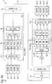
Figure 6 shows a possible embodiment of the WDMdata transport system 1 according to the present invention. In the example offigure 6 , theWDM transport system 1 comprises one 100 Gbit/sEthernet client 2 providing four 25 G Ethernet data streams DS to anoptical client interface 4 of adata transport card 3 comprising an electronic module 7 performing inter alia deskewing and forward error correction FEC. In the embodiment offigure 6 , thepluggable conversion module 5 is plugged into a socket of thedata transport card 3 and comprises a tuneable directly modulatedlaser array TDML 5A for each data stream DS. The four 25 G Ethernet signal data streams DS are modulated after forward correction FEC. The DML output is combined by means of a four to one coupler or WDM multiplexer to a WDM channel. Accordingly, the optical data signals generated by theTDML laser array 5A are coupled into at least one wavelength division multiplexing WDM channel for transport of the optical data signals via theoptical fibre 6. In the embodiment offigure 6 , a single tuneable opticalsignal reshaper TOSR 5B is integrated into thepluggable module 5 and provides a periodic 25 GHz subcarrier grid as shown in the spectrum offigures 4A, 4B . An alignment of a extinction ration or adiabatic chirp is provided in order to provide an ODB modulation at the required bit rates. The output of the tuneableoptical signal reshaper 5B can be set to a standard 100 GHz WDM grid after optional booster amplification by means of abooster amplifier 8 as shown infigure 6 . The optical data signals pass an ITU-DWDM 9 of the WDM system and are transmitted via theoptical fibre 6 to a staticdispersion compensator DCF 10 and an ITU-T-DWDM 11 at the receiving side. The data transport card 3-2 at the receiving end can comprise apreamplifier 12 for amplitude amplification of the received optical data signals. The data transport card 3-2 further comprises a socket for plugging in a pluggable conversion module 5-2 having in the shown embodiment a TWDMtuneable WDM filter 5C and aphotodiode array 5D for converting the decoupled WDM subchannels into data streams DS processed by receivers RX as shown infigure 6 . As can be seen infigure 6 , the receive end data transport card 3-2 also comprises an electronic module 7-2 and an optical client interface 4-2 for supplying four 25 GBit/sec data streams to a 100 GBE Ethernet client 2-2. The functions of the electronic module 7 can be adapted by one or several control signals CRTL activating or deactivating different subunits and adjusting parameters of said subunits. -
Figure 7 shows a further embodiment of a WDMdata transport system 1 according to the present invention wherein a 100 GBE client supplies 2-1 100 GbE SR 10 I/F data streams to the interface 4-1 of the data transport card 3-1 on the transmitting side. In the embodiment as shown infigure 7 , the tuneableoptical signal reshaper 5B is formed by two 3 dB power couplers connected on the output side to a 25 G interleaving unit. In an alternative embodiment, the two 3 dB power couplers can be formed by interleaving units as well. The provision of cascaded interleaving units reduces further the bit error rate BER of the transmitted optical data signals. -
Figure 8 shows a further possible embodiment of a WDMdata transport system 1 according to the present invention. In this exemplary embodiment, four separate clients 2A-1, 2B-1, 2C-1, 2D-1 are provided on the transmitting side each generating a 16 G or a 20 G data stream DS applied to the data stream interface 4-1 of the data transport card 3-1 on the transmitting side. In the embodiment as shown infigure 8 , the output signal of thebooster amplifier 8 is provided to aWDM demultiplexer 13 provided on the data transport card 3-1. The data transport card 3-2 on the receiving side comprises acorresponding WDM multiplexer 14. The output data streams are supplied to four separate clients 2A-2 to 2D-4. -
Figure 9 shows a further embodiment of a WDMdata transport system 1 according to the present invention having a data transport card 3-1 on the transmitting side for receiving a pluggable conversion module 5-1 having four tuneable optical signal reshapers TOSR and wavelength lockers WL for each data stream DS. The wavelength lockers WL as shown in the different embodiments are provided for locking the WDM subchannel frequencies. -
Figure 10 shows a further exemplary embodiment of a WDMdata transport system 1 according to the present invention having four separate clients 2A-1, 2B-1, 2C-1, 2D-1 on the transmitting and receiving side 2A-2, 2B-2, 2C-2, 2D-2 each generating or receiving a 16 G or 20 G data stream. Furthermore, the pluggable module 5-1 on the transmitting side comprises a single tuneable opticalsignal reshaper TOSR 5B. In a possible embodiment, theTWDM 5D of the pluggable module 5-2 on the receiving side can be thermically tuned. -
Figure 11 shows a further exemplary embodiment of a WDMdata transport system 1 according to the present invention. The has embodiment shows a client having a QSFP (Quadruple Signal Form Factor Pluggable) providing 40 GBs Infiniband data stream to a QSFP interface 4-1 of a data transport card 3-1. The electronic module 7-1 is formed by an FPGA unit as shown infigure 11 . The arrangement as shown infigure 11 can support IBQDR x 4 or 4 x 10 G or 40 GBE data streams. The arrangement can be extended to QDR x 12 data streams. -
Figure 12 shows a flowchart of a possible embodiment of a method for transporting data via anoptical fibre 6. - In a first step S1, high speed data streams DS are received via an
interface 4 from at least one orseveral clients 2. - In a further step S2, the received data streams DS are converted into optical data signals and coupled into at least one wavelength division multiplexing channel WDM having several WDM subchannels WDMS for transporting said optical data signals via the
optical fibre 6. - In a further step S3, the optical data signals received via the
optical fibre 6 in different wavelength division multiplexing subchannels WDMS of at least one wavelength division multiplexing channel WDMS which has for example a predetermined bandwidth of 100 GHz, are decoupled to data streams for at least one receivingclient 2. - In a further step S4, the decoupled data streams are supplied to the
clients 2 on the receiving side. - In a possible embodiment, the method for data transport as shown in the flowchart of
figure 12 is performed on the basis of a hardware platform in real time. - In an alternative embodiment, the method is performed by a computer program comprising a instructions for performing the method as shown in
figure 12 . - In a possible embodiment, this computer program is loaded from a data carrier storing said computer program.
- In a possible embodiment, the WDM
data transport system 1 according to the present invention as shown in the different embodiments is configurable depending on the length of theoptical fibre 6, in particular, thelaser array 5A and the tuneable opticalsignal reshaper TOSR 5B can be configured to meet the different requirements of different network , environments. -
Figures 13A, 13B show two embodiments for implementing a tuneableoptical signal reshaper 5B as employed by the WDMdata transport system 1 according to the present invention. - In a possible embodiment, the tuneable
optical signal reshaper 5B as shown infigures 13A, 13B is formed by a separate device or by a separate pluggable module which can be plugged into the motherboard of the data transport card 3-1. - In a possible embodiment, the invention provides a flexible 100 GBE data transport system for one or multiple high speed data signals over an
optical fibre 6. - The WDM
data transport system 1 according to the present invention provides different configurations supporting different environments and requirements with a relatively low complexity. The WDMdata transport system 1 according to the present invention can be used for a wide range of different data stream formats such as Ethernet Fibre Channel or InfiniBand. Furthermore, it can be used for different kinds of optical signal modulation formats. By activating or deactivating subunits of the electronic module 7, it is possible to provide low latency variants. - In a possible embodiment, the
laser array 5A is tuneable whereas in other embodiments thelaser array 5A is not tuneable. If the laser array 5-1 is tuneable, it is in a preferred embodiment tuned in response to a feedback control signal sent back from the receiving side via an embedded communication channel ECC. In a possible embodiment, another data transport channel is used for sending the feedback control signal to thetuneable laser array 5A.
Claims (15)
- A data transport card (3), comprising:an interface (4) to receive high-speed data streams, DS, from at least one client (2);socket means adapted for the plug-in of a pluggable conversion module (5), the pluggable conversion module (5) integrated into a housing of the data transport card (3);the pluggable conversion module (5) plugged into said socket means, converting said data streams, DS, into optical data signals and coupling these optical data signals into at least one wavelength division multiplexing, WDM, channel for transport of said optical data signals via an optical fibre (6),wherein said wavelength division multiplexing, WDM, channel has a predetermined bandwidth and comprises a number of WDM subchannels corresponding to a number N of received data streams, DS,wherein said pluggable conversion module (5) comprises at least one tuneable optical signal reshaper, TOSR, (5B) being adaptable to the bandwidth and to the spacing of said WDM subchannels to optimize WDM subchannel power levels, and to minimize crosstalk,wherein said tuneable optical signal reshaper, TOSR, (5B) is provided for spectrum-shaping of said WDM subchannels,wherein WDM subchannel bandwidths and the spacing of the subchannel center frequencies are adjusted to minimize a bit error rate, BER, of said optical data signals, andwherein said tuneable optical signal reshaper, TOSR, (5B) is tunable in response to a feedback control signal from a receive end data transport card (3-2) sent via an inband or outband embedded communication channel, ECC, via said optical fibre (6).
- The data transport card according to claim 1, wherein said wavelength division multiplexing, WDM, channel is a 10C GHz WDM channel comprising four 25 GHz WDM subchannels or two 50 GHz WDM subchannels.
- The data transport card according to claims 1 or 2, wherein said pluggable conversion module (5) comprises a laser array (5A) for converting said data streams, DS, into said optical data signals.
- The data transport card according to claim 3, wherein said laser array (5A) is a directly modulated, DML, laser array or an externally modulated, EML, laser array.
- The data transport card according to claim 3, wherein said laser array (5A) is tuneable by the feedback control signal from the receive end data transport card (3-2).
- The data transport card according to claim 5, wherein said WDM subchannel power levels, P, and the WDM subchannel center-frequencies are set by said tuneable laser array (5A) in response to said feedback control signal to minimize the bit error rate, BER, of said transported optical data signals.
- The data transport card according to claims 1 to 6, wherein said pluggable conversion module (5) comprises a wavelength locker, WL, which locks the WDM subchannel frequencies.
- The data transport card according to claims 1 to 6, wherein said pluggable conversion module (5) is tuneable over an adjustable number of WDM subchannels.
- The data transport card according to claims 1 to 8, wherein said optical data signals comprise an optical duo-binary, ODB, modulation format, an amplitude modulation format or a phase modulation format.
- The data transport card according to claims 1 to 9, wherein an electronic module (7) is provided, said electronic module (7) comprising:a mapping and framing unit which maps the data streams, DS, into ODU-data frames,a monitory unit which monitors data integrity,a FEC unit which performs a forward error correction, FEC, of said ODU-data frames, anda deskewing unit for performing deskewing of said data streams, DS.
- The data transport card according to claims 1 to 10, wherein said data streams, DS, provided by said at least one client (2) comprise high speed Ethernet data streams, high speed Fibre Channel data streams and high speed InfiniBand data streams, each having a bitrate of more than 4 Gbit/sec.
- The data transport card according to claim 10, wherein said electronic module (7) is a FPGA-unit.
- The data transport card according to claim 1, wherein the data transport card is a bidirectional data transport card (3) wherein the data stream interface (4) is configured to input data streams from the at least one client (2) and to output data streams to the at least one client (2); and
the pluggable conversion module (5) having means for converting said input data streams into optical data signals for coupling these optical data signals into WDM subchannels of at least one wavelength division multiplexing, WDM, channel for transport of said optical data signals via an optical fibre (6) and
means for converting optical data signals received via said optical fibre (6) in different wavelength multiplexing, WDM, subchannels of at least one wavelength division multiplexing, WDM, channel into said output data streams. - A method for transporting data using a data transport card (3) according to one or more of claims 1-13, comprising the following steps:plugging the pluggable conversion module (5) into socket means such that the pluggable conversion module (5) is integrated into the housing of the data transport card (3) ;receiving (S1) data streams, DS, from at least one client;converting (S2) said data streams, DS, into optical data signals and coupling these optical data signals into wavelength division multiplexing, WDM, subchannels of at least one wavelength division multiplexing, WDM, channel for transport said optical data signals via an optical fibre (6);reconverting (S3) the optical data signals received by said optical fibre (6) in the different wavelength division multiplexing, WDM, sub channels of said at least one wavelength division multiplexing, WDM, channel into data streams, DS,; andsupplying said reconverted data streams, DS, to at least one client (2).
- The method according to claim 14, wherein the WDM-subchannel spacing is adapted.
Priority Applications (2)
| Application Number | Priority Date | Filing Date | Title |
|---|---|---|---|
| EP09167376.4A EP2290860B1 (en) | 2009-08-06 | 2009-08-06 | A pluggable conversion module for a data transport card of a wavelength division multiplexing system |
| US12/851,946 US8483565B2 (en) | 2009-08-06 | 2010-08-06 | Pluggable conversion module for a data transport card of a wavelength division multiplexing system |
Applications Claiming Priority (1)
| Application Number | Priority Date | Filing Date | Title |
|---|---|---|---|
| EP09167376.4A EP2290860B1 (en) | 2009-08-06 | 2009-08-06 | A pluggable conversion module for a data transport card of a wavelength division multiplexing system |
Publications (2)
| Publication Number | Publication Date |
|---|---|
| EP2290860A1 EP2290860A1 (en) | 2011-03-02 |
| EP2290860B1 true EP2290860B1 (en) | 2021-03-31 |
Family
ID=41382443
Family Applications (1)
| Application Number | Title | Priority Date | Filing Date |
|---|---|---|---|
| EP09167376.4A Active EP2290860B1 (en) | 2009-08-06 | 2009-08-06 | A pluggable conversion module for a data transport card of a wavelength division multiplexing system |
Country Status (2)
| Country | Link |
|---|---|
| US (1) | US8483565B2 (en) |
| EP (1) | EP2290860B1 (en) |
Families Citing this family (18)
| Publication number | Priority date | Publication date | Assignee | Title |
|---|---|---|---|---|
| US8768170B2 (en) * | 2009-06-29 | 2014-07-01 | Oracle International Corporation | Optical device with reduced thermal tuning energy |
| US8718097B2 (en) * | 2010-09-17 | 2014-05-06 | Nec Laboratories America, Inc. | Rate selection for channel selection in flexible WDM networks |
| US8913899B2 (en) * | 2010-12-07 | 2014-12-16 | Alcatel Lucent | Distribution of optical power in an optical transport system |
| WO2012106686A2 (en) * | 2011-02-04 | 2012-08-09 | Price Lucinda | Color storage and transmission systems and methods |
| JP2013239950A (en) * | 2012-05-16 | 2013-11-28 | Nec Corp | Optical repeater and optical transmission system using the same |
| US8989591B2 (en) | 2012-06-06 | 2015-03-24 | Techsys Insights | Remote optical demarcation point |
| US9014558B2 (en) * | 2012-06-06 | 2015-04-21 | Techsys Insights | Client grooming interface |
| US9178610B1 (en) * | 2013-03-14 | 2015-11-03 | Google Inc. | Optical loopback in a wavelength division multiplexing system |
| EP2782286B1 (en) * | 2013-03-22 | 2019-08-21 | Mitsubishi Electric R&D Centre Europe B.V. | Method and device for determining whether a configuration of an optical transmission interface has to be adjusted |
| US9253120B1 (en) * | 2013-10-10 | 2016-02-02 | Qlogic, Corporation | Systems and methods for high speed data processing at a network port |
| US9639498B2 (en) * | 2013-12-27 | 2017-05-02 | Dell Products L.P. | Protocol conversion system |
| KR102140057B1 (en) * | 2014-01-20 | 2020-07-31 | 삼성전자 주식회사 | Data interface method having de-skew function and Apparatus there-of |
| JP6485189B2 (en) * | 2015-04-23 | 2019-03-20 | 富士通株式会社 | Optical transmission system and optical transmission device |
| US9548817B1 (en) * | 2015-06-19 | 2017-01-17 | Inphi Corporation | Small form factor transmitting device |
| JP6825248B2 (en) * | 2016-07-01 | 2021-02-03 | 富士通オプティカルコンポーネンツ株式会社 | Optical receivers, optical transceivers using them, and optical signal reception control methods |
| US9900103B1 (en) * | 2016-11-02 | 2018-02-20 | Alcatel-Lucent Usa Inc. | Optical transceiver having an interface circuit with a routing capability |
| US10523325B2 (en) * | 2017-05-18 | 2019-12-31 | Broadband International, Inc. | Combined equalizer and attenuator for reverse path optical nodes and methods for making and using same |
| US10985841B1 (en) * | 2020-01-29 | 2021-04-20 | Hewlett Packard Enterprise Development Lp | Wavelength division multiplexing wavelength translator |
Citations (4)
| Publication number | Priority date | Publication date | Assignee | Title |
|---|---|---|---|---|
| US20040047637A1 (en) * | 2002-09-06 | 2004-03-11 | Paracer, Inc. | Transponder assembly for use with parallel optics modules in fiber optic communications systems |
| US20060291785A1 (en) * | 2005-06-27 | 2006-12-28 | Marc Epitaux | Optical transponder module with dual board flexible circuit |
| US20080050074A1 (en) * | 2006-08-25 | 2008-02-28 | John Dallesasse | 10gbase-lx4 optical transceiver in xfp package |
| US20080069570A1 (en) * | 2006-09-15 | 2008-03-20 | John Dallesasse | Optical transceiver for 100 Gigabit/second transmission |
Family Cites Families (9)
| Publication number | Priority date | Publication date | Assignee | Title |
|---|---|---|---|---|
| EP1436869B1 (en) * | 2001-10-09 | 2016-06-01 | Infinera Corporation | Transmitter photonic integrated circuit |
| US7359641B2 (en) * | 2003-07-28 | 2008-04-15 | Emcore Corporation | Modular optical transceiver |
| JP5059601B2 (en) * | 2004-04-15 | 2012-10-24 | インフィネラ コーポレイション | Coolerless integrated circuit and floating wavelength grid photonic integrated circuit (PIC) for WDM transmission networks |
| JP4571054B2 (en) * | 2005-09-30 | 2010-10-27 | 富士通株式会社 | Optical wavelength control method and system |
| US7941053B2 (en) * | 2006-10-19 | 2011-05-10 | Emcore Corporation | Optical transceiver for 40 gigabit/second transmission |
| TWI360964B (en) * | 2006-11-08 | 2012-03-21 | Finisar Corp | Serialization/deserialization for use in optoelect |
| US8666257B2 (en) * | 2007-05-24 | 2014-03-04 | Finisar Corporation | Optoelectronic devices with intelligent transmitter modules |
| US8260150B2 (en) * | 2008-04-25 | 2012-09-04 | Finisar Corporation | Passive wave division multiplexed transmitter having a directly modulated laser array |
| US8068742B2 (en) * | 2008-07-10 | 2011-11-29 | Finisar Corporation | Phase shift keyed modulation of optical signal using chirp managed laser |
-
2009
- 2009-08-06 EP EP09167376.4A patent/EP2290860B1/en active Active
-
2010
- 2010-08-06 US US12/851,946 patent/US8483565B2/en active Active
Patent Citations (4)
| Publication number | Priority date | Publication date | Assignee | Title |
|---|---|---|---|---|
| US20040047637A1 (en) * | 2002-09-06 | 2004-03-11 | Paracer, Inc. | Transponder assembly for use with parallel optics modules in fiber optic communications systems |
| US20060291785A1 (en) * | 2005-06-27 | 2006-12-28 | Marc Epitaux | Optical transponder module with dual board flexible circuit |
| US20080050074A1 (en) * | 2006-08-25 | 2008-02-28 | John Dallesasse | 10gbase-lx4 optical transceiver in xfp package |
| US20080069570A1 (en) * | 2006-09-15 | 2008-03-20 | John Dallesasse | Optical transceiver for 100 Gigabit/second transmission |
Non-Patent Citations (3)
| Title |
|---|
| ANTOSIK R ED - MARCINIAK M: "Super-channel architectures for in-service capacity expansion of CWDM/DWDM systems", TRANSPARENT OPTICAL NETWORKS, 2003. PROCEEDINGS OF 2003 5TH INTERNATIO NAL CONFERENCE ON WARSAW, POLAND 29 JUNE-3 JULY 2003, PISCATAWAY, NJ, USA,IEEE, US, vol. 2, 29 June 2003 (2003-06-29), pages 84 - 86, XP010680699, ISBN: 978-0-7803-7816-2, DOI: 10.1109/ICTON.2003.1263150 * |
| JEN BUS: "What is new in WDM sources?", PROCCEDINGS OF SPIE, PO BOX 10 BELLINGHAM WA 98227-0010 USA, 2004, XP040192859 * |
| SAJJAD HUSSAIN ET AL: "CWDM and OEO Transport Architectures -IEE Paper.doc CWDM and OEO Transport Architectures", CONFERENCE "FUTURE CHALLENGES AND OPPORTUNITIES FOR DWDM AND CWDM IN THE PHOTONIC NETWORK", 11 June 2004 (2004-06-11), XP055180611, Retrieved from the Internet <URL:http://citeseerx.ist.psu.edu/viewdoc/download?doi=10.1.1.196.6562&rep=rep1&type=pdf> [retrieved on 20150331] * |
Also Published As
| Publication number | Publication date |
|---|---|
| EP2290860A1 (en) | 2011-03-02 |
| US20110033188A1 (en) | 2011-02-10 |
| US8483565B2 (en) | 2013-07-09 |
Similar Documents
| Publication | Publication Date | Title |
|---|---|---|
| EP2290860B1 (en) | A pluggable conversion module for a data transport card of a wavelength division multiplexing system | |
| US7203422B2 (en) | Optical network unit, wavelength splitter, and optical wavelength-division multiplexing access system | |
| US9385814B2 (en) | Wavelength tunable array for data communications | |
| US6236499B1 (en) | Highly scalable modular optical amplifier based subsystem | |
| US20150063807A1 (en) | Optical data transmission system | |
| CN102710361B (en) | A kind of distributed base station signal transmission system and communication system | |
| US20080131125A1 (en) | Loopback-type wavelength division multiplexing passive optical network system | |
| US20050025486A1 (en) | Bi-directional wavelength division multiplexing module | |
| US6661973B1 (en) | Optical transmission systems, apparatuses, and methods | |
| WO2006116519A1 (en) | Methods and apparatuses to increase wavelength channels in a wavelength-division-multiplexing passive-optical-network | |
| US7519296B2 (en) | Optical demultiplexing method and optical multiplexing method, and optical transmission apparatus using same | |
| EP2913943A1 (en) | Optical communication with spatially multiplexed optical packet signals | |
| WO2010009533A1 (en) | Wdm pon rf/video broadcast overlay | |
| EP0991217A2 (en) | Low cost WDM system | |
| Boffi et al. | Multi-Tb/s sustainable MAN scenario enabled by VCSEL-based innovative technological solutions | |
| US6400478B1 (en) | Wavelength-division-multiplexed optical transmission system with expanded bidirectional transmission capacity over a single fiber | |
| US20070177873A1 (en) | Hybrid passive optical network | |
| US7805077B2 (en) | Scalable and movable DWDM usage of CWDM networks | |
| US7486890B2 (en) | Optical transmission apparatus and method | |
| US20140363161A1 (en) | Optical signal switching device and optical transmission system | |
| US11038614B2 (en) | Optical system including a reconfigurable optical add/drop multiplexer and filters | |
| JP5911104B2 (en) | Optical demultiplexing transmission apparatus, control method, and optical demultiplexing transmission control system | |
| US8842987B2 (en) | Security in multiwavelength optical networks | |
| US10735126B1 (en) | Splitter-based colorless-directionless-contentionless reconfigurable optical add/drop multiplexer | |
| US7609970B2 (en) | Add/drop node for an optical communications network |
Legal Events
| Date | Code | Title | Description |
|---|---|---|---|
| PUAI | Public reference made under article 153(3) epc to a published international application that has entered the european phase |
Free format text: ORIGINAL CODE: 0009012 |
|
| 17P | Request for examination filed |
Effective date: 20101123 |
|
| AK | Designated contracting states |
Kind code of ref document: A1 Designated state(s): AT BE BG CH CY CZ DE DK EE ES FI FR GB GR HR HU IE IS IT LI LT LU LV MC MK MT NL NO PL PT RO SE SI SK SM TR |
|
| AX | Request for extension of the european patent |
Extension state: AL BA RS |
|
| RAP1 | Party data changed (applicant data changed or rights of an application transferred) |
Owner name: ADVA OPTICAL NETWORKING SE |
|
| STAA | Information on the status of an ep patent application or granted ep patent |
Free format text: STATUS: EXAMINATION IS IN PROGRESS |
|
| GRAP | Despatch of communication of intention to grant a patent |
Free format text: ORIGINAL CODE: EPIDOSNIGR1 |
|
| STAA | Information on the status of an ep patent application or granted ep patent |
Free format text: STATUS: GRANT OF PATENT IS INTENDED |
|
| INTG | Intention to grant announced |
Effective date: 20201124 |
|
| GRAS | Grant fee paid |
Free format text: ORIGINAL CODE: EPIDOSNIGR3 |
|
| GRAA | (expected) grant |
Free format text: ORIGINAL CODE: 0009210 |
|
| STAA | Information on the status of an ep patent application or granted ep patent |
Free format text: STATUS: THE PATENT HAS BEEN GRANTED |
|
| AK | Designated contracting states |
Kind code of ref document: B1 Designated state(s): AT BE BG CH CY CZ DE DK EE ES FI FR GB GR HR HU IE IS IT LI LT LU LV MC MK MT NL NO PL PT RO SE SI SK SM TR |
|
| REG | Reference to a national code |
Ref country code: GB Ref legal event code: FG4D Ref country code: CH Ref legal event code: EP |
|
| REG | Reference to a national code |
Ref country code: AT Ref legal event code: REF Ref document number: 1378141 Country of ref document: AT Kind code of ref document: T Effective date: 20210415 |
|
| REG | Reference to a national code |
Ref country code: DE Ref legal event code: R096 Ref document number: 602009063513 Country of ref document: DE |
|
| REG | Reference to a national code |
Ref country code: IE Ref legal event code: FG4D |
|
| REG | Reference to a national code |
Ref country code: LT Ref legal event code: MG9D |
|
| PG25 | Lapsed in a contracting state [announced via postgrant information from national office to epo] |
Ref country code: NO Free format text: LAPSE BECAUSE OF FAILURE TO SUBMIT A TRANSLATION OF THE DESCRIPTION OR TO PAY THE FEE WITHIN THE PRESCRIBED TIME-LIMIT Effective date: 20210630 Ref country code: BG Free format text: LAPSE BECAUSE OF FAILURE TO SUBMIT A TRANSLATION OF THE DESCRIPTION OR TO PAY THE FEE WITHIN THE PRESCRIBED TIME-LIMIT Effective date: 20210630 Ref country code: FI Free format text: LAPSE BECAUSE OF FAILURE TO SUBMIT A TRANSLATION OF THE DESCRIPTION OR TO PAY THE FEE WITHIN THE PRESCRIBED TIME-LIMIT Effective date: 20210331 Ref country code: HR Free format text: LAPSE BECAUSE OF FAILURE TO SUBMIT A TRANSLATION OF THE DESCRIPTION OR TO PAY THE FEE WITHIN THE PRESCRIBED TIME-LIMIT Effective date: 20210331 |
|
| PG25 | Lapsed in a contracting state [announced via postgrant information from national office to epo] |
Ref country code: SE Free format text: LAPSE BECAUSE OF FAILURE TO SUBMIT A TRANSLATION OF THE DESCRIPTION OR TO PAY THE FEE WITHIN THE PRESCRIBED TIME-LIMIT Effective date: 20210331 Ref country code: LV Free format text: LAPSE BECAUSE OF FAILURE TO SUBMIT A TRANSLATION OF THE DESCRIPTION OR TO PAY THE FEE WITHIN THE PRESCRIBED TIME-LIMIT Effective date: 20210331 |
|
| REG | Reference to a national code |
Ref country code: NL Ref legal event code: MP Effective date: 20210331 |
|
| REG | Reference to a national code |
Ref country code: AT Ref legal event code: MK05 Ref document number: 1378141 Country of ref document: AT Kind code of ref document: T Effective date: 20210331 |
|
| PG25 | Lapsed in a contracting state [announced via postgrant information from national office to epo] |
Ref country code: CZ Free format text: LAPSE BECAUSE OF FAILURE TO SUBMIT A TRANSLATION OF THE DESCRIPTION OR TO PAY THE FEE WITHIN THE PRESCRIBED TIME-LIMIT Effective date: 20210331 Ref country code: EE Free format text: LAPSE BECAUSE OF FAILURE TO SUBMIT A TRANSLATION OF THE DESCRIPTION OR TO PAY THE FEE WITHIN THE PRESCRIBED TIME-LIMIT Effective date: 20210331 Ref country code: NL Free format text: LAPSE BECAUSE OF FAILURE TO SUBMIT A TRANSLATION OF THE DESCRIPTION OR TO PAY THE FEE WITHIN THE PRESCRIBED TIME-LIMIT Effective date: 20210331 Ref country code: LT Free format text: LAPSE BECAUSE OF FAILURE TO SUBMIT A TRANSLATION OF THE DESCRIPTION OR TO PAY THE FEE WITHIN THE PRESCRIBED TIME-LIMIT Effective date: 20210331 Ref country code: AT Free format text: LAPSE BECAUSE OF FAILURE TO SUBMIT A TRANSLATION OF THE DESCRIPTION OR TO PAY THE FEE WITHIN THE PRESCRIBED TIME-LIMIT Effective date: 20210331 Ref country code: SM Free format text: LAPSE BECAUSE OF FAILURE TO SUBMIT A TRANSLATION OF THE DESCRIPTION OR TO PAY THE FEE WITHIN THE PRESCRIBED TIME-LIMIT Effective date: 20210331 |
|
| PG25 | Lapsed in a contracting state [announced via postgrant information from national office to epo] |
Ref country code: IS Free format text: LAPSE BECAUSE OF FAILURE TO SUBMIT A TRANSLATION OF THE DESCRIPTION OR TO PAY THE FEE WITHIN THE PRESCRIBED TIME-LIMIT Effective date: 20210731 Ref country code: RO Free format text: LAPSE BECAUSE OF FAILURE TO SUBMIT A TRANSLATION OF THE DESCRIPTION OR TO PAY THE FEE WITHIN THE PRESCRIBED TIME-LIMIT Effective date: 20210331 Ref country code: PL Free format text: LAPSE BECAUSE OF FAILURE TO SUBMIT A TRANSLATION OF THE DESCRIPTION OR TO PAY THE FEE WITHIN THE PRESCRIBED TIME-LIMIT Effective date: 20210331 Ref country code: PT Free format text: LAPSE BECAUSE OF FAILURE TO SUBMIT A TRANSLATION OF THE DESCRIPTION OR TO PAY THE FEE WITHIN THE PRESCRIBED TIME-LIMIT Effective date: 20210802 Ref country code: SK Free format text: LAPSE BECAUSE OF FAILURE TO SUBMIT A TRANSLATION OF THE DESCRIPTION OR TO PAY THE FEE WITHIN THE PRESCRIBED TIME-LIMIT Effective date: 20210331 Ref country code: ES Free format text: LAPSE BECAUSE OF FAILURE TO SUBMIT A TRANSLATION OF THE DESCRIPTION OR TO PAY THE FEE WITHIN THE PRESCRIBED TIME-LIMIT Effective date: 20210331 |
|
| REG | Reference to a national code |
Ref country code: DE Ref legal event code: R097 Ref document number: 602009063513 Country of ref document: DE |
|
| PG25 | Lapsed in a contracting state [announced via postgrant information from national office to epo] |
Ref country code: DK Free format text: LAPSE BECAUSE OF FAILURE TO SUBMIT A TRANSLATION OF THE DESCRIPTION OR TO PAY THE FEE WITHIN THE PRESCRIBED TIME-LIMIT Effective date: 20210331 |
|
| PLBE | No opposition filed within time limit |
Free format text: ORIGINAL CODE: 0009261 |
|
| STAA | Information on the status of an ep patent application or granted ep patent |
Free format text: STATUS: NO OPPOSITION FILED WITHIN TIME LIMIT |
|
| REG | Reference to a national code |
Ref country code: DE Ref legal event code: R119 Ref document number: 602009063513 Country of ref document: DE |
|
| 26N | No opposition filed |
Effective date: 20220104 |
|
| REG | Reference to a national code |
Ref country code: CH Ref legal event code: PL |
|
| PG25 | Lapsed in a contracting state [announced via postgrant information from national office to epo] |
Ref country code: MC Free format text: LAPSE BECAUSE OF FAILURE TO SUBMIT A TRANSLATION OF THE DESCRIPTION OR TO PAY THE FEE WITHIN THE PRESCRIBED TIME-LIMIT Effective date: 20210331 |
|
| REG | Reference to a national code |
Ref country code: BE Ref legal event code: MM Effective date: 20210831 |
|
| GBPC | Gb: european patent ceased through non-payment of renewal fee |
Effective date: 20210806 |
|
| PG25 | Lapsed in a contracting state [announced via postgrant information from national office to epo] |
Ref country code: LI Free format text: LAPSE BECAUSE OF NON-PAYMENT OF DUE FEES Effective date: 20210831 Ref country code: CH Free format text: LAPSE BECAUSE OF NON-PAYMENT OF DUE FEES Effective date: 20210831 |
|
| PG25 | Lapsed in a contracting state [announced via postgrant information from national office to epo] |
Ref country code: IS Free format text: LAPSE BECAUSE OF FAILURE TO SUBMIT A TRANSLATION OF THE DESCRIPTION OR TO PAY THE FEE WITHIN THE PRESCRIBED TIME-LIMIT Effective date: 20210731 Ref country code: LU Free format text: LAPSE BECAUSE OF NON-PAYMENT OF DUE FEES Effective date: 20210806 |
|
| PG25 | Lapsed in a contracting state [announced via postgrant information from national office to epo] |
Ref country code: IT Free format text: LAPSE BECAUSE OF FAILURE TO SUBMIT A TRANSLATION OF THE DESCRIPTION OR TO PAY THE FEE WITHIN THE PRESCRIBED TIME-LIMIT Effective date: 20210331 Ref country code: IE Free format text: LAPSE BECAUSE OF NON-PAYMENT OF DUE FEES Effective date: 20210806 Ref country code: GB Free format text: LAPSE BECAUSE OF NON-PAYMENT OF DUE FEES Effective date: 20210806 Ref country code: FR Free format text: LAPSE BECAUSE OF NON-PAYMENT OF DUE FEES Effective date: 20210831 Ref country code: DE Free format text: LAPSE BECAUSE OF NON-PAYMENT OF DUE FEES Effective date: 20220301 Ref country code: BE Free format text: LAPSE BECAUSE OF NON-PAYMENT OF DUE FEES Effective date: 20210831 |
|
| PG25 | Lapsed in a contracting state [announced via postgrant information from national office to epo] |
Ref country code: HU Free format text: LAPSE BECAUSE OF FAILURE TO SUBMIT A TRANSLATION OF THE DESCRIPTION OR TO PAY THE FEE WITHIN THE PRESCRIBED TIME-LIMIT; INVALID AB INITIO Effective date: 20090806 Ref country code: CY Free format text: LAPSE BECAUSE OF FAILURE TO SUBMIT A TRANSLATION OF THE DESCRIPTION OR TO PAY THE FEE WITHIN THE PRESCRIBED TIME-LIMIT Effective date: 20210331 |
|
| PG25 | Lapsed in a contracting state [announced via postgrant information from national office to epo] |
Ref country code: GR Free format text: LAPSE BECAUSE OF FAILURE TO SUBMIT A TRANSLATION OF THE DESCRIPTION OR TO PAY THE FEE WITHIN THE PRESCRIBED TIME-LIMIT Effective date: 20210331 |