EP2290494A1 - Mobile wireless communications device with reset function and related methods - Google Patents
Mobile wireless communications device with reset function and related methods Download PDFInfo
- Publication number
- EP2290494A1 EP2290494A1 EP09169186A EP09169186A EP2290494A1 EP 2290494 A1 EP2290494 A1 EP 2290494A1 EP 09169186 A EP09169186 A EP 09169186A EP 09169186 A EP09169186 A EP 09169186A EP 2290494 A1 EP2290494 A1 EP 2290494A1
- Authority
- EP
- European Patent Office
- Prior art keywords
- gpu
- processor
- reset
- display
- wireless communications
- Prior art date
- Legal status (The legal status is an assumption and is not a legal conclusion. Google has not performed a legal analysis and makes no representation as to the accuracy of the status listed.)
- Granted
Links
Images



Classifications
-
- G—PHYSICS
- G06—COMPUTING OR CALCULATING; COUNTING
- G06F—ELECTRIC DIGITAL DATA PROCESSING
- G06F1/00—Details not covered by groups G06F3/00 - G06F13/00 and G06F21/00
- G06F1/24—Resetting means
Definitions
- the present disclosure relates to the field of wireless communications, and, more particularly, to a mobile wireless communications device and related methods.
- a mobile communication device may suffer a serious software error (sometimes called a fatal software error), which can be resolved by a reset operation.
- a user could typically accomplish this reset operation by removing the power supply, i.e. a "battery pull" procedure.
- a reset switch that provided similar functionality, and other manufacturers made the reset function accessible via a software command.
- a reset operation in which the entire system is reset is often called a "hard reset operation” or a "full reset operation.”
- the typical mobile communications device may include many integrated circuits (ICs) therein, for example, a processor such as a central processing unit (CPU), a power management circuit, and a graphics processing unit (GPU) driving a display for the device.
- ICs integrated circuits
- CPU central processing unit
- power management circuit a graphics processing unit
- GPU graphics processing unit
- Each of these ICs is supplied with power controlled by the power management circuit.
- the power supplied to each of theses ICs is cycled off and on, thereby resetting all the ICs. Nonetheless, when these ICs are reset, the device may have a lengthy reboot time, thereby inconveniencing the user.
- FIG. 1 is a front view of a mobile wireless communications device according to the present disclosure.
- FIG. 2 is a schematic block diagram of the mobile wireless communications device of FIG 1 .
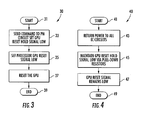
- FIG. 3 is a flowchart illustrating operation of the mobile wireless communications device of FIG 1 .
- FIG. 4 is another flowchart illustrating operation of the mobile wireless communications device of FIG 1 .
- FIG. 5 is a schematic circuit diagram of a portion of the mobile wireless communications device of FIG 1 .
- a mobile wireless communications device does not need a hard/full reset. Rather than resetting all or most of the systems, perhaps a few subsystems may be reset. Perhaps, only the CPU needs to be reset, for example. In such cases, a partial reset (or fast reset) may be performed. Positively, the partial reset feature may provide a mobile wireless communications device reset that is shorter in duration than a hard/full reset. A potential drawback to the partial reset of the CPU may be that other subsystems that do not need to be reset are adversely affected. Resetting a CPU, for example, may cause all of the CPU output pins to return to their default values. A return to the defaults values typically includes resetting the GPU, thereby causing the display to be changed, for example, the display may flicker or blank out.
- a processor such as a CPU
- the processor may be resettable along with the GPU, and the processor also may be partially resettable without resetting the GPU.
- the processor When the processor is reset without resetting the GPU, a change in the display of the device can be avoided.
- This concept will be described in the context of a mobile wireless communications device, which may include a display, and a graphics processing unit (GPU).
- the GPU is resettable and an undesirable change in the output of the display occurs, such as a flickering or a blanking, when the display is reset.
- the mobile wireless communications device also includes a wireless transceiver, and a processor cooperating with the GPU and the wireless transceiver for wireless communications.
- the processor may be resettable along with the GPU, and the processor also may be partially resettable without resetting the GPU to avoid a change in the display.
- the mobile wireless communications device may further include a power management circuit for shutting down power to the GPU and the processor during resets thereof, but maintaining power to the GPU and the processor during a partial reset of the processor.
- the processor may have an output generating a GPU reset signal during the partial reset of the processor.
- the power management circuit may have an output generating a GPU reset hold signal.
- the mobile wireless communications device may further comprise a logic circuit receiving as inputs the GPU reset signal and the GPU reset hold signal and outputting a reset control signal to the GPU.
- the logic circuit may comprise an OR gate.
- the mobile wireless communications device may further comprise a rechargeable power supply coupled to the display, the GPU, the wireless transceiver, and the processor, and a housing carrying the display, the GPU, the wireless transceiver, and the processor.
- the display may comprise a liquid crystal display
- the wireless transceiver may comprise a wireless cellular telephone transceiver.
- the method may include coupling a GPU to a display, the GPU being resettable and causing a change in the display when reset, and coupling a processor to the GPU and a wireless transceiver for wireless communications.
- the processor may be resettable along with the GPU, and the processor also may be partially resettable without resetting the GPU to avoid a change in the display.
- Another aspect is directed to a method of operating a mobile wireless communications device including a display, a graphics processing unit (GPU) being resettable and causing a change in the display when reset, a wireless transceiver, and a processor cooperating with the GPU and the wireless transceiver for wireless communications and being resettable along with the GPU.
- the method may include partially resetting the processor without resetting the GPU to avoid a change in the display.
- a mobile wireless communications device 10 illustratively includes a display 12 , and a graphics processing unit (GPU) 14 cooperating therewith to provide a graphical user interface to a user.
- the display 12 may comprise, for example, a transmissive thin film transistor liquid crystal display (LCD).
- the mobile wireless communications device 10 illustratively includes a processor 16, and a wireless transceiver 17 coupled thereto.
- the processor 16 may comprise, for example, a Marvell Tavor PV processor, as available from Marvell Semiconductor, Inc. of Santa Clara, CA.
- the wireless transceiver 17 may comprise a cellular transceiver, for example, a Global System for Mobile communications (GSM), a code division multiple access (CDMA) transceiver, and/or a Universal Mobile Telecommunications System Wideband Code Division Multiple Access (UMTS W-CDMA).
- GSM Global System for Mobile communications
- CDMA code division multiple access
- UMTS W-CDMA Universal Mobile Telecommunications System Wideband Code Division Multiple Access
- the mobile wireless communications device 10 illustratively includes a power management circuit 20 coupled to the processor 16, and a rechargeable power source, illustrated as a battery 21.
- the battery 21 is illustratively coupled to the power management circuit 20, the GPU 14, the display 12, the wireless transceiver 17, and the processor 16.
- the mobile wireless communication device 10 illustratively includes a housing 11 carrying the display 12, the GPU 14, the wireless transceiver 17, the battery 21, the power management circuit 20, and the processor 16.
- the mobile wireless communications device 10 illustratively includes a plurality of switches 13a-13c affixed to an outer surface of the housing 11.
- the mobile wireless communications device 10 further illustratively includes a logic circuit 15 coupled between the processor 16 and the GPU 14 , and between the power management circuit 20 and the GPU.
- the mobile wireless communications device 10 includes a plurality of power lines (power rails) providing power to each of the integrated circuits (ICs).
- the processor 16 cooperates with the GPU 14 and the wireless transceiver 17 for wireless communications and other mobile wireless functions, for example, GPS navigation and Internet applications. Also, as may be desirable during certain operations, the processor 16 may reset the GPU 14, thereby causing a change in the display 12 when reset, i.e. a flickering or blanking of the display.
- the processor 16 is resettable along with the GPU 14. More particularly, during a hard/full reset procedure, the power management circuit 20 may disable the power lines to all IC circuits, causing each IC circuit to reset, i.e. the power management circuit shuts down power to the GPU 14 and the processor 16 during resets thereof.
- the processor 16 also may be partially resettable without resetting the GPU 14.
- the processor 16 may access a command to reset itself without disruption of power supply from the power management circuit 20 to any of the other IC circuits.
- the processor 16 may access a command to reset itself automatically without a command from the user.
- the power management circuit 20 maintains power to the GPU 14 and the processor 16.
- the processor returns all pin outputs to default values.
- the GPU reset output pin would return to a default low value, which in the typical device would reset the GPU and display and may be described as high or low, but this is for convenience of explanation, and the concepts described herein are not necessarily limited to particular logical values.
- the GPU reset signal received from the GPU reset output pin of the processor 16 is fed into the logic circuit 15.
- the power management circuit 20 illustratively provides a GPU reset hold signal, which is also input in the logic circuit 15.
- the output of the logic circuit 15 is coupled to a reset pin of the GPU 14 and provides a reset control signal.
- the logic circuit 15 maintains the output to a high value even though the GPU reset signal from the processor goes to a low value, thereby preventing the GPU 14 and display 12 from resetting, i.e. this avoids any flickering or blanking of the display during the partial reset.
- the logic circuit 15 may comprise an OR gate. More particularly, the OR gate may receive the GPU reset signal from the processor 16 and the GPU reset hold signal from the power management circuit 20. During the partial reset operation, the processor 16 GPU reset signal goes to a low value and is OR'ed with the GPU reset hold signal of the power management circuit 20, for example, the power management IC General Purpose Input/Output (PMIC GPIO) signal. During the partial reset, the power management circuit 20 PMIC GPIO signal remains at a high value and keeps the output of the OR gate, i.e. the reset control signal, also at a high value, thereby preventing the GPU 14 and display 12 from resetting and disrupting the user experience. Indeed, in the mobile wireless communications device 10, the processor 16 may perform a partial reset without the user even noticing.
- PMIC GPIO General Purpose Input/Output
- the processor 16 begins at Block 31 and sends the power management circuit 20 a command to bring the GPU reset hold signal to a low value.
- Block 33 the processor 16 and the power management circuit 20 communicate using a multi-master serial computer bus based upon, for example, an inter-integrated circuit (I 2 C) standard.
- I 2 C inter-integrated circuit
- the processor 16 sets the GPU reset signal to a low value, which now brings the reset control signal to a low value also, thereby resetting the GPU 14 and the display 12. (Blocks 35, 37, & 39).
- the mobile wireless communications device 10 may include a pair of pull-down resistors (for example, 300 k ⁇ ) coupled to the OR gate.
- one pull-down resistor ( FIG. 5 ) is coupled to PMIC GPIO signal and the other pull-down resistor is coupled to the output of the OR gate.
- this maintains the reset control signal at a low value during a power-up operation of the mobile wireless communications device 10. More specifically, as will be appreciated by those skilled in the art, it is desirable to maintain the display 12 in a reset state during the power-up operation, which begins at Block 41.
- the PMIC GPIO signal is by default in an unconfigured state and the processor 16 GPU reset signal goes to a low value by default. Accordingly, the first pull-down resistor maintains the respective input of the OR gate at a low value, therefore keeping the reset control signal low during the power-up operation. (Block 45 ).
- the second pull-down resistor ( FIG. 5 ) coupled to the output of the OR gate is used to maintain the output at a low value during the power-up operation. More particularly, the time period of concern is prior to 1.8 Volt power application to the OR gate. In other words, the second pull-down resistor keeps the OR gate output at a low value when the OR gate is not powered. (Blocks 47 & 49). Of course, if the OR gate can maintain a low while being without power, then the second pull-down resistor may be omitted.
- FIG. 5 another embodiment of the mobile wireless communications device 10' is now described.
- the mobile wireless communications device 10' differs from the previous embodiment in that the mobile wireless communications device 10' further includes an OR gate 15' receiving the GPU reset and the GPU reset hold signals and outputting the reset control signal to the GPU.
- the mobile wireless communications device 10' further includes a pair of pull-down resistors 22'-23' .
- the method may include coupling a GPU 14 to a display 12, the GPU being resettable and causing a change in the display when reset, and coupling a processor 16 to the GPU and a wireless transceiver 17 for wireless communications.
- the processor 16 may be resettable along with the GPU 14, and the processor also may be partially resettable without resetting the GPU to avoid a change in the display 12.
- the mobile wireless communications device 10 described hereinabove may provide several benefits over the typical mobile wireless communications device. For example, mobile wireless communications device 10 experiences shorter reboot times and provides a more desirable user experience during a partial reset operation since the display 12 does not flicker or reset during aforesaid partial reset operations. Indeed, the user may be unaware that the mobile wireless communications device 10 has performed a fast reset operation.
Landscapes
- Engineering & Computer Science (AREA)
- Theoretical Computer Science (AREA)
- Physics & Mathematics (AREA)
- General Engineering & Computer Science (AREA)
- General Physics & Mathematics (AREA)
- Telephone Function (AREA)
Abstract
Description
- The present disclosure relates to the field of wireless communications, and, more particularly, to a mobile wireless communications device and related methods.
- Mobile communications devices, including but not limited to cell phones, have become an integral part of society over the last two decades. On occasion, a mobile communication device may suffer a serious software error (sometimes called a fatal software error), which can be resolved by a reset operation. In early devices, a user could typically accomplish this reset operation by removing the power supply, i.e. a "battery pull" procedure. To avoid the inconvenience of the battery pull procedure, some manufacturers provided a reset switch that provided similar functionality, and other manufacturers made the reset function accessible via a software command. A reset operation in which the entire system is reset is often called a "hard reset operation" or a "full reset operation."
- The typical mobile communications device may include many integrated circuits (ICs) therein, for example, a processor such as a central processing unit (CPU), a power management circuit, and a graphics processing unit (GPU) driving a display for the device. Each of these ICs is supplied with power controlled by the power management circuit. When the device is reset, the power supplied to each of theses ICs is cycled off and on, thereby resetting all the ICs. Nonetheless, when these ICs are reset, the device may have a lengthy reboot time, thereby inconveniencing the user.
-
FIG. 1 is a front view of a mobile wireless communications device according to the present disclosure. -
FIG. 2 is a schematic block diagram of the mobile wireless communications device ofFIG 1 . -
FIG. 3 is a flowchart illustrating operation of the mobile wireless communications device ofFIG 1 . -
FIG. 4 is another flowchart illustrating operation of the mobile wireless communications device ofFIG 1 . -
FIG. 5 is a schematic circuit diagram of a portion of the mobile wireless communications device ofFIG 1 . - In some cases, a mobile wireless communications device does not need a hard/full reset. Rather than resetting all or most of the systems, perhaps a few subsystems may be reset. Perhaps, only the CPU needs to be reset, for example. In such cases, a partial reset (or fast reset) may be performed. Positively, the partial reset feature may provide a mobile wireless communications device reset that is shorter in duration than a hard/full reset. A potential drawback to the partial reset of the CPU may be that other subsystems that do not need to be reset are adversely affected. Resetting a CPU, for example, may cause all of the CPU output pins to return to their default values. A return to the defaults values typically includes resetting the GPU, thereby causing the display to be changed, for example, the display may flicker or blank out.
- As described below, a processor, such as a CPU, may be resettable along with the GPU, and the processor also may be partially resettable without resetting the GPU. When the processor is reset without resetting the GPU, a change in the display of the device can be avoided. This concept will be described in the context of a mobile wireless communications device, which may include a display, and a graphics processing unit (GPU). The GPU is resettable and an undesirable change in the output of the display occurs, such as a flickering or a blanking, when the display is reset. The mobile wireless communications device also includes a wireless transceiver, and a processor cooperating with the GPU and the wireless transceiver for wireless communications. The processor may be resettable along with the GPU, and the processor also may be partially resettable without resetting the GPU to avoid a change in the display.
- The mobile wireless communications device may further include a power management circuit for shutting down power to the GPU and the processor during resets thereof, but maintaining power to the GPU and the processor during a partial reset of the processor. The processor may have an output generating a GPU reset signal during the partial reset of the processor. The power management circuit may have an output generating a GPU reset hold signal. The mobile wireless communications device may further comprise a logic circuit receiving as inputs the GPU reset signal and the GPU reset hold signal and outputting a reset control signal to the GPU.
- In some embodiments, the logic circuit may comprise an OR gate. The mobile wireless communications device may further comprise a rechargeable power supply coupled to the display, the GPU, the wireless transceiver, and the processor, and a housing carrying the display, the GPU, the wireless transceiver, and the processor. For example, the display may comprise a liquid crystal display, and the wireless transceiver may comprise a wireless cellular telephone transceiver.
- Another aspect is directed to a method for making a mobile wireless communications device. The method may include coupling a GPU to a display, the GPU being resettable and causing a change in the display when reset, and coupling a processor to the GPU and a wireless transceiver for wireless communications. The processor may be resettable along with the GPU, and the processor also may be partially resettable without resetting the GPU to avoid a change in the display.
- Another aspect is directed to a method of operating a mobile wireless communications device including a display, a graphics processing unit (GPU) being resettable and causing a change in the display when reset, a wireless transceiver, and a processor cooperating with the GPU and the wireless transceiver for wireless communications and being resettable along with the GPU. The method may include partially resetting the processor without resetting the GPU to avoid a change in the display.
- The present description is made with reference to the accompanying drawings, in which various embodiments are shown. However, many different embodiments may be used, and thus the description should not be construed as limited to the embodiments set forth herein. Rather, these embodiments are provided so that this disclosure will be thorough and complete. Like numbers refer to like elements throughout, and prime notation is used to indicate similar elements in alternative embodiments.
- Referring initially to
FIGS. 1-2 , a mobilewireless communications device 10 illustratively includes adisplay 12, and a graphics processing unit (GPU) 14 cooperating therewith to provide a graphical user interface to a user. Thedisplay 12 may comprise, for example, a transmissive thin film transistor liquid crystal display (LCD). The mobilewireless communications device 10 illustratively includes aprocessor 16, and awireless transceiver 17 coupled thereto. Theprocessor 16 may comprise, for example, a Marvell Tavor PV processor, as available from Marvell Semiconductor, Inc. of Santa Clara, CA. In certain embodiments, thewireless transceiver 17 may comprise a cellular transceiver, for example, a Global System for Mobile communications (GSM), a code division multiple access (CDMA) transceiver, and/or a Universal Mobile Telecommunications System Wideband Code Division Multiple Access (UMTS W-CDMA). - The mobile
wireless communications device 10 illustratively includes apower management circuit 20 coupled to theprocessor 16, and a rechargeable power source, illustrated as abattery 21. Thebattery 21 is illustratively coupled to thepower management circuit 20, theGPU 14, thedisplay 12, thewireless transceiver 17, and theprocessor 16. Also, the mobilewireless communication device 10 illustratively includes ahousing 11 carrying thedisplay 12, theGPU 14, thewireless transceiver 17, thebattery 21, thepower management circuit 20, and theprocessor 16. The mobilewireless communications device 10 illustratively includes a plurality ofswitches 13a-13c affixed to an outer surface of thehousing 11. - Further, the mobile
wireless communications device 10 further illustratively includes alogic circuit 15 coupled between theprocessor 16 and theGPU 14, and between thepower management circuit 20 and the GPU. As will be appreciated by those skilled in the art, the mobilewireless communications device 10 includes a plurality of power lines (power rails) providing power to each of the integrated circuits (ICs). - During operation, the
processor 16 cooperates with theGPU 14 and thewireless transceiver 17 for wireless communications and other mobile wireless functions, for example, GPS navigation and Internet applications. Also, as may be desirable during certain operations, theprocessor 16 may reset theGPU 14, thereby causing a change in thedisplay 12 when reset, i.e. a flickering or blanking of the display. Theprocessor 16 is resettable along with theGPU 14. More particularly, during a hard/full reset procedure, thepower management circuit 20 may disable the power lines to all IC circuits, causing each IC circuit to reset, i.e. the power management circuit shuts down power to theGPU 14 and theprocessor 16 during resets thereof. - Advantageously, the
processor 16 also may be partially resettable without resetting theGPU 14. In other words, theprocessor 16 may access a command to reset itself without disruption of power supply from thepower management circuit 20 to any of the other IC circuits. In some embodiments, theprocessor 16 may access a command to reset itself automatically without a command from the user. Further to this point, during the partial reset operation of theprocessor 16, thepower management circuit 20 maintains power to theGPU 14 and theprocessor 16. Nonetheless, during the partial reset operation of the processor 6, the processor returns all pin outputs to default values. For example, the GPU reset output pin would return to a default low value, which in the typical device would reset the GPU and display and may be described as high or low, but this is for convenience of explanation, and the concepts described herein are not necessarily limited to particular logical values. - In this mobile
wireless communications device 10, the GPU reset signal received from the GPU reset output pin of theprocessor 16 is fed into thelogic circuit 15. Thepower management circuit 20 illustratively provides a GPU reset hold signal, which is also input in thelogic circuit 15. The output of thelogic circuit 15 is coupled to a reset pin of theGPU 14 and provides a reset control signal. Advantageously, during the partial reset operation of theprocessor 16, thelogic circuit 15 maintains the output to a high value even though the GPU reset signal from the processor goes to a low value, thereby preventing theGPU 14 anddisplay 12 from resetting, i.e. this avoids any flickering or blanking of the display during the partial reset. - In some embodiments, the
logic circuit 15 may comprise an OR gate. More particularly, the OR gate may receive the GPU reset signal from theprocessor 16 and the GPU reset hold signal from thepower management circuit 20. During the partial reset operation, theprocessor 16 GPU reset signal goes to a low value and is OR'ed with the GPU reset hold signal of thepower management circuit 20, for example, the power management IC General Purpose Input/Output (PMIC GPIO) signal. During the partial reset, thepower management circuit 20 PMIC GPIO signal remains at a high value and keeps the output of the OR gate, i.e. the reset control signal, also at a high value, thereby preventing theGPU 14 anddisplay 12 from resetting and disrupting the user experience. Indeed, in the mobilewireless communications device 10, theprocessor 16 may perform a partial reset without the user even noticing. - Referring now additionally to the
flowchart 30 ofFIG. 3 , in situations where it may be desirable to force aGPU 14 anddisplay 12 reset, theprocessor 16 begins atBlock 31 and sends the power management circuit 20 a command to bring the GPU reset hold signal to a low value. (Block 33). As will be appreciated by those skilled in the art, theprocessor 16 and thepower management circuit 20 communicate using a multi-master serial computer bus based upon, for example, an inter-integrated circuit (I2C) standard. Of course, as will be appreciated by those skilled in the art, other communication standards may be used. Theprocessor 16 sets the GPU reset signal to a low value, which now brings the reset control signal to a low value also, thereby resetting theGPU 14 and thedisplay 12. (Blocks - Referring now additionally to the
flowchart 40 ofFIG. 4 , in this embodiment, the mobilewireless communications device 10 may include a pair of pull-down resistors (for example, 300 kΩ) coupled to the OR gate. In particular, one pull-down resistor (FIG. 5 ) is coupled to PMIC GPIO signal and the other pull-down resistor is coupled to the output of the OR gate. Advantageously, this maintains the reset control signal at a low value during a power-up operation of the mobilewireless communications device 10. More specifically, as will be appreciated by those skilled in the art, it is desirable to maintain thedisplay 12 in a reset state during the power-up operation, which begins atBlock 41. At power-up, (Block 43), the PMIC GPIO signal is by default in an unconfigured state and theprocessor 16 GPU reset signal goes to a low value by default. Accordingly, the first pull-down resistor maintains the respective input of the OR gate at a low value, therefore keeping the reset control signal low during the power-up operation. (Block 45). - Furthermore, the second pull-down resistor (
FIG. 5 ) coupled to the output of the OR gate is used to maintain the output at a low value during the power-up operation. More particularly, the time period of concern is prior to 1.8 Volt power application to the OR gate. In other words, the second pull-down resistor keeps the OR gate output at a low value when the OR gate is not powered. (Blocks 47 & 49). Of course, if the OR gate can maintain a low while being without power, then the second pull-down resistor may be omitted. - Referring now to
FIG. 5 , another embodiment of the mobile wireless communications device 10' is now described. In this embodiment of the mobile wireless communications device 10', those elements already discussed above with respect toFIGS. 1-2 are given prime notation and most require no further discussion herein. This embodiment differs from the previous embodiment in that the mobile wireless communications device 10' further includes an OR gate 15' receiving the GPU reset and the GPU reset hold signals and outputting the reset control signal to the GPU. Further, as discussed herein above, the mobile wireless communications device 10' further includes a pair of pull-down resistors 22'-23'. - Another aspect is directed to a method for making a mobile
wireless communications device 10. The method may include coupling aGPU 14 to adisplay 12, the GPU being resettable and causing a change in the display when reset, and coupling aprocessor 16 to the GPU and awireless transceiver 17 for wireless communications. Theprocessor 16 may be resettable along with theGPU 14, and the processor also may be partially resettable without resetting the GPU to avoid a change in thedisplay 12. - The mobile
wireless communications device 10 described hereinabove may provide several benefits over the typical mobile wireless communications device. For example, mobilewireless communications device 10 experiences shorter reboot times and provides a more desirable user experience during a partial reset operation since thedisplay 12 does not flicker or reset during aforesaid partial reset operations. Indeed, the user may be unaware that the mobilewireless communications device 10 has performed a fast reset operation. - Many modifications and other embodiments of the disclosure will come to the mind of one skilled in the art having the benefit of the teachings presented in the foregoing descriptions and the associated drawings. Therefore, it is understood that this disclosure is not to be limited to the specific embodiments disclosed, and that modifications and embodiments are intended to be included within the scope of the appended claims.
Claims (14)
- A mobile wireless communications device (10) comprising:a display (12);a graphics processing unit (GPU)(14) being resettable and causing a change in said display when reset;a wireless transceiver (17); anda processor (16) cooperating with said GPU and said wireless transceiver for wireless communications;said processor being resettable along with said GPU, and said processor also being partially resettable without resetting said GPU to avoid a change in said display.
- The mobile wireless communications device (10) according to Claim 1 further comprising a power management circuit (20) for shutting down power to said GPU and said processor (16) during resets thereof, but maintaining power to said GPU (14) and said processor during a partial reset of said processor.
- The mobile wireless communications device (10) according to Claim 2 wherein said processor (16) has an output generating a GPU (14) reset signal during the partial reset of said processor; wherein said power management circuit (20) has an output generating a GPU reset hold signal; and further comprising a logic circuit (15) receiving as inputs the GPU reset signal and the GPU reset hold signal and outputting a reset control signal to said GPU.
- The mobile wireless communications device (10) according to Claim 3 wherein said logic circuit (15) comprises an OR gate.
- The mobile wireless communications device (10) according to Claim 1 further comprising a rechargeable power supply coupled to said display, said GPU (14), said wireless transceiver (17), and said processor (16).
- The mobile wireless communications device (10) according to Claim 1 further comprising a housing (11) carrying said display (12), said GPU (14), said wireless transceiver (17), and said processor (16).
- The mobile wireless communications device (10) according to Claim 1 wherein said display (12) comprises a liquid crystal display.
- The mobile wireless communications device (10) according to Claim 1 wherein said wireless transceiver (17) comprises a wireless cellular telephone transceiver.
- A method for making a mobile wireless communications device (10) comprising:coupling a graphics processing unit (GPU)(14) to a display (12), the GPU being resettable and causing a change in the display when reset; andcoupling a processor to the GPU and a wireless transceiver (17) for wireless communications, the processor (16) being resettable along with the GPU, and the processor also being partially resettable without resetting the GPU to avoid a change in the display.
- The method according to Claim 9 further comprising coupling a power management circuit (20) to the GPU (14) and the processor (16) for shutting down power to the GPU and the processor during resets thereof, but maintaining power to the GPU and the processor during a partial reset of the processor.
- The method according to Claim 10 wherein the processor (16) has an output generating a GPU (14) reset signal during the partial reset of the processor; wherein the power management circuit (20) has an output generating a GPU reset hold signal; and further comprising coupling a logic circuit (15) to receive as inputs the GPU reset signal and the GPU reset hold signal and to output a reset control signal to the GPU.
- The method according to Claim 11 wherein the logic circuit (15) comprises an OR gate.
- The method according to Claim 9 further comprising coupling a rechargeable power supply (21) to the display (12), the GPU (14), the wireless transceiver (17), and the processor (16).
- The method according to Claim 9 further comprising providing a housing (11) to carry the display (12), the GPU (14), the wireless transceiver (17), and the processor (16).
Priority Applications (2)
| Application Number | Priority Date | Filing Date | Title |
|---|---|---|---|
| EP09169186.5A EP2290494B1 (en) | 2009-09-01 | 2009-09-01 | Mobile wireless communications device with reset function and related methods |
| CA2714243A CA2714243C (en) | 2009-09-01 | 2010-09-01 | Mobile wireless communications device with reset functions and related methods |
Applications Claiming Priority (1)
| Application Number | Priority Date | Filing Date | Title |
|---|---|---|---|
| EP09169186.5A EP2290494B1 (en) | 2009-09-01 | 2009-09-01 | Mobile wireless communications device with reset function and related methods |
Publications (2)
| Publication Number | Publication Date |
|---|---|
| EP2290494A1 true EP2290494A1 (en) | 2011-03-02 |
| EP2290494B1 EP2290494B1 (en) | 2020-04-29 |
Family
ID=41683553
Family Applications (1)
| Application Number | Title | Priority Date | Filing Date |
|---|---|---|---|
| EP09169186.5A Active EP2290494B1 (en) | 2009-09-01 | 2009-09-01 | Mobile wireless communications device with reset function and related methods |
Country Status (2)
| Country | Link |
|---|---|
| EP (1) | EP2290494B1 (en) |
| CA (1) | CA2714243C (en) |
Citations (4)
| Publication number | Priority date | Publication date | Assignee | Title |
|---|---|---|---|---|
| JPH08227328A (en) * | 1995-02-20 | 1996-09-03 | Canon Inc | Information processing system |
| US20060112263A1 (en) * | 2004-11-25 | 2006-05-25 | Via Technologies Inc. | Basic input output system and computer reset method |
| US20070050685A1 (en) * | 2005-08-23 | 2007-03-01 | Tsai Chung-Hung | Method of resetting an unresponsive system and system capable of recovering from an unresponsive condition |
| JP2008041059A (en) * | 2006-08-10 | 2008-02-21 | Toshiba Corp | Multiprocessor control apparatus and information processing apparatus |
-
2009
- 2009-09-01 EP EP09169186.5A patent/EP2290494B1/en active Active
-
2010
- 2010-09-01 CA CA2714243A patent/CA2714243C/en active Active
Patent Citations (4)
| Publication number | Priority date | Publication date | Assignee | Title |
|---|---|---|---|---|
| JPH08227328A (en) * | 1995-02-20 | 1996-09-03 | Canon Inc | Information processing system |
| US20060112263A1 (en) * | 2004-11-25 | 2006-05-25 | Via Technologies Inc. | Basic input output system and computer reset method |
| US20070050685A1 (en) * | 2005-08-23 | 2007-03-01 | Tsai Chung-Hung | Method of resetting an unresponsive system and system capable of recovering from an unresponsive condition |
| JP2008041059A (en) * | 2006-08-10 | 2008-02-21 | Toshiba Corp | Multiprocessor control apparatus and information processing apparatus |
Non-Patent Citations (1)
| Title |
|---|
| DATABASE WPI Week 199645, Derwent World Patents Index; AN 1996-452304, XP002570207 * |
Also Published As
| Publication number | Publication date |
|---|---|
| CA2714243A1 (en) | 2011-03-01 |
| CA2714243C (en) | 2016-08-02 |
| EP2290494B1 (en) | 2020-04-29 |
Similar Documents
| Publication | Publication Date | Title |
|---|---|---|
| US9063885B2 (en) | Mobile wireless communications device with reset functions and related methods | |
| US9280357B2 (en) | Configuration based on chassis identifications | |
| EP2315098A2 (en) | Enhanced fast reset in mobile wireless communication devices and associated methods | |
| US20180301109A1 (en) | Display control circuit, display control method thereof, and display apparatus | |
| JP2019519837A (en) | Fast turn-on power switch | |
| CN102339405B (en) | Data card | |
| CN112514258A (en) | Low power clock gate circuit | |
| EP4343562A1 (en) | Enabling universal core motherboard with flexible input-output ports | |
| US8922252B2 (en) | Threshold voltage dependent power-gate driver | |
| CN103092304B (en) | Power supply control method of dual graphics card module and computer device using the method | |
| US10389169B2 (en) | VBUS power switch | |
| EP2290494B1 (en) | Mobile wireless communications device with reset function and related methods | |
| CN102611078A (en) | Portable electronic device and system efficiency adjusting method thereof | |
| EP2143111B1 (en) | Sharing routing of a test signal with an alternative power supply to combinatorial logic for low power design | |
| US7493507B2 (en) | System for protecting a motherboard while a component is not connected properly to its power source | |
| WO2019133200A1 (en) | Protection circuit for decoupling a low voltage circuitry from a high voltage circuitry | |
| US20180129260A1 (en) | Bridge module and operation method thereof | |
| US20110127965A1 (en) | Battery charge-discharge path management circuit and method thereof | |
| CN110493551A (en) | A kind of display device, mainboard and control method | |
| CN108292149B (en) | Power delivery architecture for improving performance of computing systems when docked | |
| JP2003114742A (en) | Power cutoff control device | |
| KR20130123502A (en) | Portable electronic device and method for reset using the same | |
| KR101178844B1 (en) | Device of controlling a data communication and a mobile communication terminal comprising it | |
| US20070191072A1 (en) | Wireless communication device with circuit for unconnecting data input and method thereof | |
| KR101070625B1 (en) | Display apparatus |
Legal Events
| Date | Code | Title | Description |
|---|---|---|---|
| PUAI | Public reference made under article 153(3) epc to a published international application that has entered the european phase |
Free format text: ORIGINAL CODE: 0009012 |
|
| 17P | Request for examination filed |
Effective date: 20090908 |
|
| AK | Designated contracting states |
Kind code of ref document: A1 Designated state(s): AT BE BG CH CY CZ DE DK EE ES FI FR GB GR HR HU IE IS IT LI LT LU LV MC MK MT NL NO PL PT RO SE SI SK SM TR |
|
| AX | Request for extension of the european patent |
Extension state: AL BA RS |
|
| RAP1 | Party data changed (applicant data changed or rights of an application transferred) |
Owner name: BLACKBERRY LIMITED |
|
| RAP1 | Party data changed (applicant data changed or rights of an application transferred) |
Owner name: BLACKBERRY LIMITED |
|
| 17Q | First examination report despatched |
Effective date: 20160223 |
|
| STAA | Information on the status of an ep patent application or granted ep patent |
Free format text: STATUS: EXAMINATION IS IN PROGRESS |
|
| GRAP | Despatch of communication of intention to grant a patent |
Free format text: ORIGINAL CODE: EPIDOSNIGR1 |
|
| STAA | Information on the status of an ep patent application or granted ep patent |
Free format text: STATUS: GRANT OF PATENT IS INTENDED |
|
| INTG | Intention to grant announced |
Effective date: 20191210 |
|
| GRAS | Grant fee paid |
Free format text: ORIGINAL CODE: EPIDOSNIGR3 |
|
| GRAJ | Information related to disapproval of communication of intention to grant by the applicant or resumption of examination proceedings by the epo deleted |
Free format text: ORIGINAL CODE: EPIDOSDIGR1 |
|
| GRAL | Information related to payment of fee for publishing/printing deleted |
Free format text: ORIGINAL CODE: EPIDOSDIGR3 |
|
| STAA | Information on the status of an ep patent application or granted ep patent |
Free format text: STATUS: EXAMINATION IS IN PROGRESS |
|
| GRAP | Despatch of communication of intention to grant a patent |
Free format text: ORIGINAL CODE: EPIDOSNIGR1 |
|
| STAA | Information on the status of an ep patent application or granted ep patent |
Free format text: STATUS: GRANT OF PATENT IS INTENDED |
|
| GRAA | (expected) grant |
Free format text: ORIGINAL CODE: 0009210 |
|
| STAA | Information on the status of an ep patent application or granted ep patent |
Free format text: STATUS: THE PATENT HAS BEEN GRANTED |
|
| INTC | Intention to grant announced (deleted) | ||
| INTG | Intention to grant announced |
Effective date: 20200312 |
|
| AK | Designated contracting states |
Kind code of ref document: B1 Designated state(s): AT BE BG CH CY CZ DE DK EE ES FI FR GB GR HR HU IE IS IT LI LT LU LV MC MK MT NL NO PL PT RO SE SI SK SM TR |
|
| REG | Reference to a national code |
Ref country code: GB Ref legal event code: FG4D |
|
| REG | Reference to a national code |
Ref country code: CH Ref legal event code: EP |
|
| REG | Reference to a national code |
Ref country code: AT Ref legal event code: REF Ref document number: 1264284 Country of ref document: AT Kind code of ref document: T Effective date: 20200515 |
|
| REG | Reference to a national code |
Ref country code: DE Ref legal event code: R096 Ref document number: 602009061868 Country of ref document: DE |
|
| REG | Reference to a national code |
Ref country code: IE Ref legal event code: FG4D |
|
| REG | Reference to a national code |
Ref country code: NL Ref legal event code: MP Effective date: 20200429 |
|
| REG | Reference to a national code |
Ref country code: LT Ref legal event code: MG4D |
|
| PG25 | Lapsed in a contracting state [announced via postgrant information from national office to epo] |
Ref country code: LT Free format text: LAPSE BECAUSE OF FAILURE TO SUBMIT A TRANSLATION OF THE DESCRIPTION OR TO PAY THE FEE WITHIN THE PRESCRIBED TIME-LIMIT Effective date: 20200429 Ref country code: FI Free format text: LAPSE BECAUSE OF FAILURE TO SUBMIT A TRANSLATION OF THE DESCRIPTION OR TO PAY THE FEE WITHIN THE PRESCRIBED TIME-LIMIT Effective date: 20200429 Ref country code: PT Free format text: LAPSE BECAUSE OF FAILURE TO SUBMIT A TRANSLATION OF THE DESCRIPTION OR TO PAY THE FEE WITHIN THE PRESCRIBED TIME-LIMIT Effective date: 20200831 Ref country code: NO Free format text: LAPSE BECAUSE OF FAILURE TO SUBMIT A TRANSLATION OF THE DESCRIPTION OR TO PAY THE FEE WITHIN THE PRESCRIBED TIME-LIMIT Effective date: 20200729 Ref country code: IS Free format text: LAPSE BECAUSE OF FAILURE TO SUBMIT A TRANSLATION OF THE DESCRIPTION OR TO PAY THE FEE WITHIN THE PRESCRIBED TIME-LIMIT Effective date: 20200829 Ref country code: SE Free format text: LAPSE BECAUSE OF FAILURE TO SUBMIT A TRANSLATION OF THE DESCRIPTION OR TO PAY THE FEE WITHIN THE PRESCRIBED TIME-LIMIT Effective date: 20200429 Ref country code: GR Free format text: LAPSE BECAUSE OF FAILURE TO SUBMIT A TRANSLATION OF THE DESCRIPTION OR TO PAY THE FEE WITHIN THE PRESCRIBED TIME-LIMIT Effective date: 20200730 |
|
| REG | Reference to a national code |
Ref country code: AT Ref legal event code: MK05 Ref document number: 1264284 Country of ref document: AT Kind code of ref document: T Effective date: 20200429 |
|
| PG25 | Lapsed in a contracting state [announced via postgrant information from national office to epo] |
Ref country code: HR Free format text: LAPSE BECAUSE OF FAILURE TO SUBMIT A TRANSLATION OF THE DESCRIPTION OR TO PAY THE FEE WITHIN THE PRESCRIBED TIME-LIMIT Effective date: 20200429 Ref country code: LV Free format text: LAPSE BECAUSE OF FAILURE TO SUBMIT A TRANSLATION OF THE DESCRIPTION OR TO PAY THE FEE WITHIN THE PRESCRIBED TIME-LIMIT Effective date: 20200429 Ref country code: BG Free format text: LAPSE BECAUSE OF FAILURE TO SUBMIT A TRANSLATION OF THE DESCRIPTION OR TO PAY THE FEE WITHIN THE PRESCRIBED TIME-LIMIT Effective date: 20200729 |
|
| PG25 | Lapsed in a contracting state [announced via postgrant information from national office to epo] |
Ref country code: NL Free format text: LAPSE BECAUSE OF FAILURE TO SUBMIT A TRANSLATION OF THE DESCRIPTION OR TO PAY THE FEE WITHIN THE PRESCRIBED TIME-LIMIT Effective date: 20200429 |
|
| PG25 | Lapsed in a contracting state [announced via postgrant information from national office to epo] |
Ref country code: RO Free format text: LAPSE BECAUSE OF FAILURE TO SUBMIT A TRANSLATION OF THE DESCRIPTION OR TO PAY THE FEE WITHIN THE PRESCRIBED TIME-LIMIT Effective date: 20200429 Ref country code: CZ Free format text: LAPSE BECAUSE OF FAILURE TO SUBMIT A TRANSLATION OF THE DESCRIPTION OR TO PAY THE FEE WITHIN THE PRESCRIBED TIME-LIMIT Effective date: 20200429 Ref country code: AT Free format text: LAPSE BECAUSE OF FAILURE TO SUBMIT A TRANSLATION OF THE DESCRIPTION OR TO PAY THE FEE WITHIN THE PRESCRIBED TIME-LIMIT Effective date: 20200429 Ref country code: IT Free format text: LAPSE BECAUSE OF FAILURE TO SUBMIT A TRANSLATION OF THE DESCRIPTION OR TO PAY THE FEE WITHIN THE PRESCRIBED TIME-LIMIT Effective date: 20200429 Ref country code: ES Free format text: LAPSE BECAUSE OF FAILURE TO SUBMIT A TRANSLATION OF THE DESCRIPTION OR TO PAY THE FEE WITHIN THE PRESCRIBED TIME-LIMIT Effective date: 20200429 Ref country code: DK Free format text: LAPSE BECAUSE OF FAILURE TO SUBMIT A TRANSLATION OF THE DESCRIPTION OR TO PAY THE FEE WITHIN THE PRESCRIBED TIME-LIMIT Effective date: 20200429 Ref country code: SM Free format text: LAPSE BECAUSE OF FAILURE TO SUBMIT A TRANSLATION OF THE DESCRIPTION OR TO PAY THE FEE WITHIN THE PRESCRIBED TIME-LIMIT Effective date: 20200429 Ref country code: EE Free format text: LAPSE BECAUSE OF FAILURE TO SUBMIT A TRANSLATION OF THE DESCRIPTION OR TO PAY THE FEE WITHIN THE PRESCRIBED TIME-LIMIT Effective date: 20200429 |
|
| REG | Reference to a national code |
Ref country code: DE Ref legal event code: R097 Ref document number: 602009061868 Country of ref document: DE |
|
| PG25 | Lapsed in a contracting state [announced via postgrant information from national office to epo] |
Ref country code: SK Free format text: LAPSE BECAUSE OF FAILURE TO SUBMIT A TRANSLATION OF THE DESCRIPTION OR TO PAY THE FEE WITHIN THE PRESCRIBED TIME-LIMIT Effective date: 20200429 Ref country code: PL Free format text: LAPSE BECAUSE OF FAILURE TO SUBMIT A TRANSLATION OF THE DESCRIPTION OR TO PAY THE FEE WITHIN THE PRESCRIBED TIME-LIMIT Effective date: 20200429 |
|
| PLBE | No opposition filed within time limit |
Free format text: ORIGINAL CODE: 0009261 |
|
| STAA | Information on the status of an ep patent application or granted ep patent |
Free format text: STATUS: NO OPPOSITION FILED WITHIN TIME LIMIT |
|
| 26N | No opposition filed |
Effective date: 20210201 |
|
| PG25 | Lapsed in a contracting state [announced via postgrant information from national office to epo] |
Ref country code: MC Free format text: LAPSE BECAUSE OF FAILURE TO SUBMIT A TRANSLATION OF THE DESCRIPTION OR TO PAY THE FEE WITHIN THE PRESCRIBED TIME-LIMIT Effective date: 20200429 |
|
| REG | Reference to a national code |
Ref country code: CH Ref legal event code: PL |
|
| PG25 | Lapsed in a contracting state [announced via postgrant information from national office to epo] |
Ref country code: SI Free format text: LAPSE BECAUSE OF FAILURE TO SUBMIT A TRANSLATION OF THE DESCRIPTION OR TO PAY THE FEE WITHIN THE PRESCRIBED TIME-LIMIT Effective date: 20200429 |
|
| REG | Reference to a national code |
Ref country code: BE Ref legal event code: MM Effective date: 20200930 |
|
| PG25 | Lapsed in a contracting state [announced via postgrant information from national office to epo] |
Ref country code: LU Free format text: LAPSE BECAUSE OF NON-PAYMENT OF DUE FEES Effective date: 20200901 |
|
| PG25 | Lapsed in a contracting state [announced via postgrant information from national office to epo] |
Ref country code: CH Free format text: LAPSE BECAUSE OF NON-PAYMENT OF DUE FEES Effective date: 20200930 Ref country code: BE Free format text: LAPSE BECAUSE OF NON-PAYMENT OF DUE FEES Effective date: 20200930 Ref country code: IE Free format text: LAPSE BECAUSE OF NON-PAYMENT OF DUE FEES Effective date: 20200901 Ref country code: LI Free format text: LAPSE BECAUSE OF NON-PAYMENT OF DUE FEES Effective date: 20200930 |
|
| PG25 | Lapsed in a contracting state [announced via postgrant information from national office to epo] |
Ref country code: TR Free format text: LAPSE BECAUSE OF FAILURE TO SUBMIT A TRANSLATION OF THE DESCRIPTION OR TO PAY THE FEE WITHIN THE PRESCRIBED TIME-LIMIT Effective date: 20200429 Ref country code: MT Free format text: LAPSE BECAUSE OF FAILURE TO SUBMIT A TRANSLATION OF THE DESCRIPTION OR TO PAY THE FEE WITHIN THE PRESCRIBED TIME-LIMIT Effective date: 20200429 Ref country code: CY Free format text: LAPSE BECAUSE OF FAILURE TO SUBMIT A TRANSLATION OF THE DESCRIPTION OR TO PAY THE FEE WITHIN THE PRESCRIBED TIME-LIMIT Effective date: 20200429 |
|
| PG25 | Lapsed in a contracting state [announced via postgrant information from national office to epo] |
Ref country code: MK Free format text: LAPSE BECAUSE OF FAILURE TO SUBMIT A TRANSLATION OF THE DESCRIPTION OR TO PAY THE FEE WITHIN THE PRESCRIBED TIME-LIMIT Effective date: 20200429 |
|
| REG | Reference to a national code |
Ref country code: DE Ref legal event code: R081 Ref document number: 602009061868 Country of ref document: DE Owner name: MALIKIE INNOVATIONS LTD., IE Free format text: FORMER OWNER: BLACKBERRY LIMITED, WATERLOO, ONTARIO, CA |
|
| PGFP | Annual fee paid to national office [announced via postgrant information from national office to epo] |
Ref country code: DE Payment date: 20250926 Year of fee payment: 17 |
|
| PGFP | Annual fee paid to national office [announced via postgrant information from national office to epo] |
Ref country code: GB Payment date: 20250923 Year of fee payment: 17 |
|
| PGFP | Annual fee paid to national office [announced via postgrant information from national office to epo] |
Ref country code: FR Payment date: 20250925 Year of fee payment: 17 |