EP2289984A1 - Laminate film and composite film - Google Patents
Laminate film and composite film Download PDFInfo
- Publication number
- EP2289984A1 EP2289984A1 EP10173974A EP10173974A EP2289984A1 EP 2289984 A1 EP2289984 A1 EP 2289984A1 EP 10173974 A EP10173974 A EP 10173974A EP 10173974 A EP10173974 A EP 10173974A EP 2289984 A1 EP2289984 A1 EP 2289984A1
- Authority
- EP
- European Patent Office
- Prior art keywords
- laminate film
- film
- film according
- laminate
- organic layer
- Prior art date
- Legal status (The legal status is an assumption and is not a legal conclusion. Google has not performed a legal analysis and makes no representation as to the accuracy of the status listed.)
- Withdrawn
Links
- 239000005001 laminate film Substances 0.000 title claims abstract description 93
- 239000002131 composite material Substances 0.000 title claims description 23
- 239000010410 layer Substances 0.000 claims abstract description 85
- 239000012044 organic layer Substances 0.000 claims abstract description 59
- 239000000758 substrate Substances 0.000 claims abstract description 46
- VYPSYNLAJGMNEJ-UHFFFAOYSA-N Silicium dioxide Chemical compound O=[Si]=O VYPSYNLAJGMNEJ-UHFFFAOYSA-N 0.000 claims abstract description 22
- 229910052814 silicon oxide Inorganic materials 0.000 claims abstract description 22
- 238000000034 method Methods 0.000 claims description 23
- 239000000203 mixture Substances 0.000 claims description 20
- NIXOWILDQLNWCW-UHFFFAOYSA-M Acrylate Chemical compound [O-]C(=O)C=C NIXOWILDQLNWCW-UHFFFAOYSA-M 0.000 claims description 17
- 239000010419 fine particle Substances 0.000 claims description 13
- 239000006087 Silane Coupling Agent Substances 0.000 claims description 9
- 239000003086 colorant Substances 0.000 claims description 8
- PNEYBMLMFCGWSK-UHFFFAOYSA-N Alumina Chemical compound [O-2].[O-2].[O-2].[Al+3].[Al+3] PNEYBMLMFCGWSK-UHFFFAOYSA-N 0.000 claims description 6
- 238000001771 vacuum deposition Methods 0.000 claims description 5
- GWEVSGVZZGPLCZ-UHFFFAOYSA-N Titan oxide Chemical compound O=[Ti]=O GWEVSGVZZGPLCZ-UHFFFAOYSA-N 0.000 claims description 4
- OGIDPMRJRNCKJF-UHFFFAOYSA-N titanium oxide Inorganic materials [Ti]=O OGIDPMRJRNCKJF-UHFFFAOYSA-N 0.000 claims description 4
- 239000006229 carbon black Substances 0.000 claims description 3
- RVTZCBVAJQQJTK-UHFFFAOYSA-N oxygen(2-);zirconium(4+) Chemical compound [O-2].[O-2].[Zr+4] RVTZCBVAJQQJTK-UHFFFAOYSA-N 0.000 claims description 3
- 229910001928 zirconium oxide Inorganic materials 0.000 claims description 3
- 238000004519 manufacturing process Methods 0.000 claims description 2
- 230000004888 barrier function Effects 0.000 abstract description 19
- 239000010408 film Substances 0.000 description 85
- 150000001875 compounds Chemical class 0.000 description 18
- 230000001070 adhesive effect Effects 0.000 description 17
- 239000000853 adhesive Substances 0.000 description 16
- 229920005989 resin Polymers 0.000 description 14
- 239000011347 resin Substances 0.000 description 14
- 239000012790 adhesive layer Substances 0.000 description 10
- 239000002985 plastic film Substances 0.000 description 10
- 229920006255 plastic film Polymers 0.000 description 10
- 238000001723 curing Methods 0.000 description 8
- 238000000151 deposition Methods 0.000 description 8
- 229910052738 indium Inorganic materials 0.000 description 8
- 239000000463 material Substances 0.000 description 8
- 238000005259 measurement Methods 0.000 description 8
- QVGXLLKOCUKJST-UHFFFAOYSA-N atomic oxygen Chemical compound [O] QVGXLLKOCUKJST-UHFFFAOYSA-N 0.000 description 7
- 230000015572 biosynthetic process Effects 0.000 description 7
- 229910052802 copper Inorganic materials 0.000 description 7
- 239000010949 copper Substances 0.000 description 7
- 229910052760 oxygen Inorganic materials 0.000 description 7
- 239000001301 oxygen Substances 0.000 description 7
- 229920002799 BoPET Polymers 0.000 description 6
- RYGMFSIKBFXOCR-UHFFFAOYSA-N Copper Chemical compound [Cu] RYGMFSIKBFXOCR-UHFFFAOYSA-N 0.000 description 6
- BUGBHKTXTAQXES-UHFFFAOYSA-N Selenium Chemical compound [Se] BUGBHKTXTAQXES-UHFFFAOYSA-N 0.000 description 6
- 238000000576 coating method Methods 0.000 description 6
- NIHNNTQXNPWCJQ-UHFFFAOYSA-N fluorene Chemical compound C1=CC=C2CC3=CC=CC=C3C2=C1 NIHNNTQXNPWCJQ-UHFFFAOYSA-N 0.000 description 6
- APFVFJFRJDLVQX-UHFFFAOYSA-N indium atom Chemical compound [In] APFVFJFRJDLVQX-UHFFFAOYSA-N 0.000 description 6
- 229910052751 metal Inorganic materials 0.000 description 6
- 239000002184 metal Substances 0.000 description 6
- 239000004417 polycarbonate Substances 0.000 description 6
- -1 polyethylene terephthalate Polymers 0.000 description 6
- 238000006116 polymerization reaction Methods 0.000 description 6
- 229910052711 selenium Inorganic materials 0.000 description 6
- 239000011669 selenium Substances 0.000 description 6
- 230000035699 permeability Effects 0.000 description 5
- 239000004065 semiconductor Substances 0.000 description 5
- 230000037303 wrinkles Effects 0.000 description 5
- GYHNNYVSQQEPJS-UHFFFAOYSA-N Gallium Chemical compound [Ga] GYHNNYVSQQEPJS-UHFFFAOYSA-N 0.000 description 4
- 229910052733 gallium Inorganic materials 0.000 description 4
- 239000002346 layers by function Substances 0.000 description 4
- 239000006224 matting agent Substances 0.000 description 4
- 150000004767 nitrides Chemical class 0.000 description 4
- 239000000126 substance Substances 0.000 description 4
- XLYOFNOQVPJJNP-UHFFFAOYSA-N water Chemical compound O XLYOFNOQVPJJNP-UHFFFAOYSA-N 0.000 description 4
- IJGRMHOSHXDMSA-UHFFFAOYSA-N Atomic nitrogen Chemical compound N#N IJGRMHOSHXDMSA-UHFFFAOYSA-N 0.000 description 3
- 0 C=CC(*CC(COc(cc1)ccc1C1=CC=CCC1)S)=O Chemical compound C=CC(*CC(COc(cc1)ccc1C1=CC=CCC1)S)=O 0.000 description 3
- 125000002723 alicyclic group Chemical group 0.000 description 3
- 125000003118 aryl group Chemical group 0.000 description 3
- 229920001577 copolymer Polymers 0.000 description 3
- 239000003999 initiator Substances 0.000 description 3
- QSHDDOUJBYECFT-UHFFFAOYSA-N mercury Chemical compound [Hg] QSHDDOUJBYECFT-UHFFFAOYSA-N 0.000 description 3
- 229910052753 mercury Inorganic materials 0.000 description 3
- 239000000178 monomer Substances 0.000 description 3
- 229920000515 polycarbonate Polymers 0.000 description 3
- 229920005668 polycarbonate resin Polymers 0.000 description 3
- 239000004431 polycarbonate resin Substances 0.000 description 3
- 230000005855 radiation Effects 0.000 description 3
- 238000001029 thermal curing Methods 0.000 description 3
- JBRZTFJDHDCESZ-UHFFFAOYSA-N AsGa Chemical compound [As]#[Ga] JBRZTFJDHDCESZ-UHFFFAOYSA-N 0.000 description 2
- 229940126062 Compound A Drugs 0.000 description 2
- NLDMNSXOCDLTTB-UHFFFAOYSA-N Heterophylliin A Natural products O1C2COC(=O)C3=CC(O)=C(O)C(O)=C3C3=C(O)C(O)=C(O)C=C3C(=O)OC2C(OC(=O)C=2C=C(O)C(O)=C(O)C=2)C(O)C1OC(=O)C1=CC(O)=C(O)C(O)=C1 NLDMNSXOCDLTTB-UHFFFAOYSA-N 0.000 description 2
- 239000004642 Polyimide Substances 0.000 description 2
- NINIDFKCEFEMDL-UHFFFAOYSA-N Sulfur Chemical compound [S] NINIDFKCEFEMDL-UHFFFAOYSA-N 0.000 description 2
- 239000000654 additive Substances 0.000 description 2
- 229910052782 aluminium Inorganic materials 0.000 description 2
- 238000007611 bar coating method Methods 0.000 description 2
- IISBACLAFKSPIT-UHFFFAOYSA-N bisphenol A Chemical compound C=1C=C(O)C=CC=1C(C)(C)C1=CC=C(O)C=C1 IISBACLAFKSPIT-UHFFFAOYSA-N 0.000 description 2
- RPPBZEBXAAZZJH-UHFFFAOYSA-N cadmium telluride Chemical compound [Te]=[Cd] RPPBZEBXAAZZJH-UHFFFAOYSA-N 0.000 description 2
- 230000015556 catabolic process Effects 0.000 description 2
- 239000011248 coating agent Substances 0.000 description 2
- 238000006731 degradation reaction Methods 0.000 description 2
- 230000008021 deposition Effects 0.000 description 2
- ZUOUZKKEUPVFJK-UHFFFAOYSA-N diphenyl Chemical group C1=CC=CC=C1C1=CC=CC=C1 ZUOUZKKEUPVFJK-UHFFFAOYSA-N 0.000 description 2
- 239000005038 ethylene vinyl acetate Substances 0.000 description 2
- 239000007789 gas Substances 0.000 description 2
- 239000011521 glass Substances 0.000 description 2
- 150000002500 ions Chemical class 0.000 description 2
- 238000010030 laminating Methods 0.000 description 2
- 239000007788 liquid Substances 0.000 description 2
- 229910044991 metal oxide Inorganic materials 0.000 description 2
- 150000004706 metal oxides Chemical class 0.000 description 2
- 229910052757 nitrogen Inorganic materials 0.000 description 2
- 229920003207 poly(ethylene-2,6-naphthalate) Polymers 0.000 description 2
- 229920001200 poly(ethylene-vinyl acetate) Polymers 0.000 description 2
- 229920002492 poly(sulfone) Polymers 0.000 description 2
- 229920001230 polyarylate Polymers 0.000 description 2
- 229920001225 polyester resin Polymers 0.000 description 2
- 239000004645 polyester resin Substances 0.000 description 2
- 239000011112 polyethylene naphthalate Substances 0.000 description 2
- 229920000139 polyethylene terephthalate Polymers 0.000 description 2
- 239000005020 polyethylene terephthalate Substances 0.000 description 2
- 229920001721 polyimide Polymers 0.000 description 2
- 239000003505 polymerization initiator Substances 0.000 description 2
- 229920000098 polyolefin Polymers 0.000 description 2
- 230000008569 process Effects 0.000 description 2
- 239000011241 protective layer Substances 0.000 description 2
- LVTJOONKWUXEFR-FZRMHRINSA-N protoneodioscin Natural products O(C[C@@H](CC[C@]1(O)[C@H](C)[C@@H]2[C@]3(C)[C@H]([C@H]4[C@@H]([C@]5(C)C(=CC4)C[C@@H](O[C@@H]4[C@H](O[C@H]6[C@@H](O)[C@@H](O)[C@@H](O)[C@H](C)O6)[C@@H](O)[C@H](O[C@H]6[C@@H](O)[C@@H](O)[C@@H](O)[C@H](C)O6)[C@H](CO)O4)CC5)CC3)C[C@@H]2O1)C)[C@H]1[C@H](O)[C@H](O)[C@H](O)[C@@H](CO)O1 LVTJOONKWUXEFR-FZRMHRINSA-N 0.000 description 2
- 229910052717 sulfur Inorganic materials 0.000 description 2
- 239000011593 sulfur Substances 0.000 description 2
- 229920005992 thermoplastic resin Polymers 0.000 description 2
- 239000010409 thin film Substances 0.000 description 2
- 229910052718 tin Inorganic materials 0.000 description 2
- 239000011135 tin Substances 0.000 description 2
- 239000010936 titanium Substances 0.000 description 2
- 229910052719 titanium Inorganic materials 0.000 description 2
- 150000003673 urethanes Chemical class 0.000 description 2
- 229910052725 zinc Inorganic materials 0.000 description 2
- QNODIIQQMGDSEF-UHFFFAOYSA-N (1-hydroxycyclohexyl)-phenylmethanone Chemical compound C=1C=CC=CC=1C(=O)C1(O)CCCCC1 QNODIIQQMGDSEF-UHFFFAOYSA-N 0.000 description 1
- ODIGIKRIUKFKHP-UHFFFAOYSA-N (n-propan-2-yloxycarbonylanilino) acetate Chemical compound CC(C)OC(=O)N(OC(C)=O)C1=CC=CC=C1 ODIGIKRIUKFKHP-UHFFFAOYSA-N 0.000 description 1
- KWVGIHKZDCUPEU-UHFFFAOYSA-N 2,2-dimethoxy-2-phenylacetophenone Chemical compound C=1C=CC=CC=1C(OC)(OC)C(=O)C1=CC=CC=C1 KWVGIHKZDCUPEU-UHFFFAOYSA-N 0.000 description 1
- ZWEHNKRNPOVVGH-UHFFFAOYSA-N 2-Butanone Chemical compound CCC(C)=O ZWEHNKRNPOVVGH-UHFFFAOYSA-N 0.000 description 1
- GJKGAPPUXSSCFI-UHFFFAOYSA-N 2-Hydroxy-4'-(2-hydroxyethoxy)-2-methylpropiophenone Chemical compound CC(C)(O)C(=O)C1=CC=C(OCCO)C=C1 GJKGAPPUXSSCFI-UHFFFAOYSA-N 0.000 description 1
- FIOCEWASVZHBTK-UHFFFAOYSA-N 2-[2-(2-oxo-2-phenylacetyl)oxyethoxy]ethyl 2-oxo-2-phenylacetate Chemical compound C=1C=CC=CC=1C(=O)C(=O)OCCOCCOC(=O)C(=O)C1=CC=CC=C1 FIOCEWASVZHBTK-UHFFFAOYSA-N 0.000 description 1
- UHFFVFAKEGKNAQ-UHFFFAOYSA-N 2-benzyl-2-(dimethylamino)-1-(4-morpholin-4-ylphenyl)butan-1-one Chemical compound C=1C=C(N2CCOCC2)C=CC=1C(=O)C(CC)(N(C)C)CC1=CC=CC=C1 UHFFVFAKEGKNAQ-UHFFFAOYSA-N 0.000 description 1
- XMLYCEVDHLAQEL-UHFFFAOYSA-N 2-hydroxy-2-methyl-1-phenylpropan-1-one Chemical compound CC(C)(O)C(=O)C1=CC=CC=C1 XMLYCEVDHLAQEL-UHFFFAOYSA-N 0.000 description 1
- LWRBVKNFOYUCNP-UHFFFAOYSA-N 2-methyl-1-(4-methylsulfanylphenyl)-2-morpholin-4-ylpropan-1-one Chemical compound C1=CC(SC)=CC=C1C(=O)C(C)(C)N1CCOCC1 LWRBVKNFOYUCNP-UHFFFAOYSA-N 0.000 description 1
- 101001074560 Arabidopsis thaliana Aquaporin PIP1-2 Proteins 0.000 description 1
- SPFPPNUDPFUCEZ-UHFFFAOYSA-N C=CC(OCC(CCc1c(CCC=C2)c2c(cccc2)c2c1)S)=O Chemical compound C=CC(OCC(CCc1c(CCC=C2)c2c(cccc2)c2c1)S)=O SPFPPNUDPFUCEZ-UHFFFAOYSA-N 0.000 description 1
- 229910052684 Cerium Inorganic materials 0.000 description 1
- GPXJNWSHGFTCBW-UHFFFAOYSA-N Indium phosphide Chemical compound [In]#P GPXJNWSHGFTCBW-UHFFFAOYSA-N 0.000 description 1
- CERQOIWHTDAKMF-UHFFFAOYSA-M Methacrylate Chemical compound CC(=C)C([O-])=O CERQOIWHTDAKMF-UHFFFAOYSA-M 0.000 description 1
- 239000004696 Poly ether ether ketone Substances 0.000 description 1
- 229920012266 Poly(ether sulfone) PES Polymers 0.000 description 1
- 239000004695 Polyether sulfone Substances 0.000 description 1
- 239000004697 Polyetherimide Substances 0.000 description 1
- 238000003848 UV Light-Curing Methods 0.000 description 1
- 238000004833 X-ray photoelectron spectroscopy Methods 0.000 description 1
- 241000234314 Zingiber Species 0.000 description 1
- 235000006886 Zingiber officinale Nutrition 0.000 description 1
- 125000004054 acenaphthylenyl group Chemical group C1(=CC2=CC=CC3=CC=CC1=C23)* 0.000 description 1
- 150000001252 acrylic acid derivatives Chemical class 0.000 description 1
- 239000004480 active ingredient Substances 0.000 description 1
- 229910021417 amorphous silicon Inorganic materials 0.000 description 1
- 125000005577 anthracene group Chemical group 0.000 description 1
- 125000003828 azulenyl group Chemical group 0.000 description 1
- TXVHTIQJNYSSKO-UHFFFAOYSA-N benzo[e]pyrene Chemical group C1=CC=C2C3=CC=CC=C3C3=CC=CC4=CC=C1C2=C34 TXVHTIQJNYSSKO-UHFFFAOYSA-N 0.000 description 1
- 230000001588 bifunctional effect Effects 0.000 description 1
- ZDZHCHYQNPQSGG-UHFFFAOYSA-N binaphthyl group Chemical group C1(=CC=CC2=CC=CC=C12)C1=CC=CC2=CC=CC=C12 ZDZHCHYQNPQSGG-UHFFFAOYSA-N 0.000 description 1
- 239000004305 biphenyl Chemical group 0.000 description 1
- 235000010290 biphenyl Nutrition 0.000 description 1
- 125000002529 biphenylenyl group Chemical group C1(=CC=CC=2C3=CC=CC=C3C12)* 0.000 description 1
- 229910052799 carbon Inorganic materials 0.000 description 1
- 229920002678 cellulose Polymers 0.000 description 1
- 239000001913 cellulose Substances 0.000 description 1
- 238000006243 chemical reaction Methods 0.000 description 1
- 239000003795 chemical substances by application Substances 0.000 description 1
- 125000005578 chrysene group Chemical group 0.000 description 1
- 230000000052 comparative effect Effects 0.000 description 1
- 238000004132 cross linking Methods 0.000 description 1
- 238000000354 decomposition reaction Methods 0.000 description 1
- 230000007423 decrease Effects 0.000 description 1
- 230000003247 decreasing effect Effects 0.000 description 1
- 230000005611 electricity Effects 0.000 description 1
- 238000011156 evaluation Methods 0.000 description 1
- 238000001125 extrusion Methods 0.000 description 1
- 239000000945 filler Substances 0.000 description 1
- 235000008397 ginger Nutrition 0.000 description 1
- 230000009477 glass transition Effects 0.000 description 1
- 238000007756 gravure coating Methods 0.000 description 1
- 239000003779 heat-resistant material Substances 0.000 description 1
- 239000004615 ingredient Substances 0.000 description 1
- 239000011256 inorganic filler Substances 0.000 description 1
- 229910003475 inorganic filler Inorganic materials 0.000 description 1
- 229910052809 inorganic oxide Inorganic materials 0.000 description 1
- 238000009413 insulation Methods 0.000 description 1
- 230000001678 irradiating effect Effects 0.000 description 1
- 238000007759 kiss coating Methods 0.000 description 1
- 239000004611 light stabiliser Substances 0.000 description 1
- 239000002075 main ingredient Substances 0.000 description 1
- 150000002736 metal compounds Chemical class 0.000 description 1
- 150000002739 metals Chemical class 0.000 description 1
- 125000005641 methacryl group Chemical group 0.000 description 1
- 229910021421 monocrystalline silicon Inorganic materials 0.000 description 1
- 125000001624 naphthyl group Chemical group 0.000 description 1
- QJGQUHMNIGDVPM-UHFFFAOYSA-N nitrogen group Chemical group [N] QJGQUHMNIGDVPM-UHFFFAOYSA-N 0.000 description 1
- 229910052755 nonmetal Inorganic materials 0.000 description 1
- 230000003287 optical effect Effects 0.000 description 1
- 125000002080 perylenyl group Chemical group C1(=CC=C2C=CC=C3C4=CC=CC5=CC=CC(C1=C23)=C45)* 0.000 description 1
- 125000001792 phenanthrenyl group Chemical group C1(=CC=CC=2C3=CC=CC=C3C=CC12)* 0.000 description 1
- 125000001997 phenyl group Chemical group [H]C1=C([H])C([H])=C(*)C([H])=C1[H] 0.000 description 1
- 125000001388 picenyl group Chemical group C1(=CC=CC2=CC=C3C4=CC=C5C=CC=CC5=C4C=CC3=C21)* 0.000 description 1
- 229920006122 polyamide resin Polymers 0.000 description 1
- 229920002312 polyamide-imide Polymers 0.000 description 1
- 229910021420 polycrystalline silicon Inorganic materials 0.000 description 1
- 229920006393 polyether sulfone Polymers 0.000 description 1
- 229920002530 polyetherether ketone Polymers 0.000 description 1
- 229920001601 polyetherimide Polymers 0.000 description 1
- 230000000379 polymerizing effect Effects 0.000 description 1
- 229920005672 polyolefin resin Polymers 0.000 description 1
- 229920001296 polysiloxane Polymers 0.000 description 1
- 229920005990 polystyrene resin Polymers 0.000 description 1
- 229920005749 polyurethane resin Polymers 0.000 description 1
- 229920002620 polyvinyl fluoride Polymers 0.000 description 1
- KCTAWXVAICEBSD-UHFFFAOYSA-N prop-2-enoyloxy prop-2-eneperoxoate Chemical compound C=CC(=O)OOOC(=O)C=C KCTAWXVAICEBSD-UHFFFAOYSA-N 0.000 description 1
- 230000001681 protective effect Effects 0.000 description 1
- 238000010926 purge Methods 0.000 description 1
- 125000005581 pyrene group Chemical group 0.000 description 1
- 230000009467 reduction Effects 0.000 description 1
- 230000002040 relaxant effect Effects 0.000 description 1
- LIVNPJMFVYWSIS-UHFFFAOYSA-N silicon monoxide Chemical compound [Si-]#[O+] LIVNPJMFVYWSIS-UHFFFAOYSA-N 0.000 description 1
- 239000002904 solvent Substances 0.000 description 1
- 238000006467 substitution reaction Methods 0.000 description 1
- 229910052715 tantalum Inorganic materials 0.000 description 1
- 125000001935 tetracenyl group Chemical group C1(=CC=CC2=CC3=CC4=CC=CC=C4C=C3C=C12)* 0.000 description 1
- 238000009823 thermal lamination Methods 0.000 description 1
- 239000012780 transparent material Substances 0.000 description 1
- 125000005580 triphenylene group Chemical group 0.000 description 1
- 239000006097 ultraviolet radiation absorber Substances 0.000 description 1
- 239000012463 white pigment Substances 0.000 description 1
- 239000011701 zinc Substances 0.000 description 1
Images
Classifications
-
- B—PERFORMING OPERATIONS; TRANSPORTING
- B32—LAYERED PRODUCTS
- B32B—LAYERED PRODUCTS, i.e. PRODUCTS BUILT-UP OF STRATA OF FLAT OR NON-FLAT, e.g. CELLULAR OR HONEYCOMB, FORM
- B32B27/00—Layered products comprising a layer of synthetic resin
- B32B27/06—Layered products comprising a layer of synthetic resin as the main or only constituent of a layer, which is next to another layer of the same or of a different material
- B32B27/08—Layered products comprising a layer of synthetic resin as the main or only constituent of a layer, which is next to another layer of the same or of a different material of synthetic resin
-
- C—CHEMISTRY; METALLURGY
- C08—ORGANIC MACROMOLECULAR COMPOUNDS; THEIR PREPARATION OR CHEMICAL WORKING-UP; COMPOSITIONS BASED THEREON
- C08J—WORKING-UP; GENERAL PROCESSES OF COMPOUNDING; AFTER-TREATMENT NOT COVERED BY SUBCLASSES C08B, C08C, C08F, C08G or C08H
- C08J7/00—Chemical treatment or coating of shaped articles made of macromolecular substances
- C08J7/04—Coating
- C08J7/042—Coating with two or more layers, where at least one layer of a composition contains a polymer binder
- C08J7/0423—Coating with two or more layers, where at least one layer of a composition contains a polymer binder with at least one layer of inorganic material and at least one layer of a composition containing a polymer binder
-
- C—CHEMISTRY; METALLURGY
- C08—ORGANIC MACROMOLECULAR COMPOUNDS; THEIR PREPARATION OR CHEMICAL WORKING-UP; COMPOSITIONS BASED THEREON
- C08J—WORKING-UP; GENERAL PROCESSES OF COMPOUNDING; AFTER-TREATMENT NOT COVERED BY SUBCLASSES C08B, C08C, C08F, C08G or C08H
- C08J7/00—Chemical treatment or coating of shaped articles made of macromolecular substances
- C08J7/04—Coating
- C08J7/043—Improving the adhesiveness of the coatings per se, e.g. forming primers
-
- C—CHEMISTRY; METALLURGY
- C08—ORGANIC MACROMOLECULAR COMPOUNDS; THEIR PREPARATION OR CHEMICAL WORKING-UP; COMPOSITIONS BASED THEREON
- C08J—WORKING-UP; GENERAL PROCESSES OF COMPOUNDING; AFTER-TREATMENT NOT COVERED BY SUBCLASSES C08B, C08C, C08F, C08G or C08H
- C08J7/00—Chemical treatment or coating of shaped articles made of macromolecular substances
- C08J7/04—Coating
- C08J7/048—Forming gas barrier coatings
-
- H—ELECTRICITY
- H10—SEMICONDUCTOR DEVICES; ELECTRIC SOLID-STATE DEVICES NOT OTHERWISE PROVIDED FOR
- H10F—INORGANIC SEMICONDUCTOR DEVICES SENSITIVE TO INFRARED RADIATION, LIGHT, ELECTROMAGNETIC RADIATION OF SHORTER WAVELENGTH OR CORPUSCULAR RADIATION
- H10F19/00—Integrated devices, or assemblies of multiple devices, comprising at least one photovoltaic cell covered by group H10F10/00, e.g. photovoltaic modules
- H10F19/80—Encapsulations or containers for integrated devices, or assemblies of multiple devices, having photovoltaic cells
- H10F19/85—Protective back sheets
-
- C—CHEMISTRY; METALLURGY
- C08—ORGANIC MACROMOLECULAR COMPOUNDS; THEIR PREPARATION OR CHEMICAL WORKING-UP; COMPOSITIONS BASED THEREON
- C08J—WORKING-UP; GENERAL PROCESSES OF COMPOUNDING; AFTER-TREATMENT NOT COVERED BY SUBCLASSES C08B, C08C, C08F, C08G or C08H
- C08J2367/00—Characterised by the use of polyesters obtained by reactions forming a carboxylic ester link in the main chain; Derivatives of such polymers
- C08J2367/02—Polyesters derived from dicarboxylic acids and dihydroxy compounds
-
- Y—GENERAL TAGGING OF NEW TECHNOLOGICAL DEVELOPMENTS; GENERAL TAGGING OF CROSS-SECTIONAL TECHNOLOGIES SPANNING OVER SEVERAL SECTIONS OF THE IPC; TECHNICAL SUBJECTS COVERED BY FORMER USPC CROSS-REFERENCE ART COLLECTIONS [XRACs] AND DIGESTS
- Y02—TECHNOLOGIES OR APPLICATIONS FOR MITIGATION OR ADAPTATION AGAINST CLIMATE CHANGE
- Y02E—REDUCTION OF GREENHOUSE GAS [GHG] EMISSIONS, RELATED TO ENERGY GENERATION, TRANSMISSION OR DISTRIBUTION
- Y02E10/00—Energy generation through renewable energy sources
- Y02E10/50—Photovoltaic [PV] energy
-
- Y—GENERAL TAGGING OF NEW TECHNOLOGICAL DEVELOPMENTS; GENERAL TAGGING OF CROSS-SECTIONAL TECHNOLOGIES SPANNING OVER SEVERAL SECTIONS OF THE IPC; TECHNICAL SUBJECTS COVERED BY FORMER USPC CROSS-REFERENCE ART COLLECTIONS [XRACs] AND DIGESTS
- Y10—TECHNICAL SUBJECTS COVERED BY FORMER USPC
- Y10T—TECHNICAL SUBJECTS COVERED BY FORMER US CLASSIFICATION
- Y10T428/00—Stock material or miscellaneous articles
- Y10T428/24—Structurally defined web or sheet [e.g., overall dimension, etc.]
- Y10T428/24355—Continuous and nonuniform or irregular surface on layer or component [e.g., roofing, etc.]
-
- Y—GENERAL TAGGING OF NEW TECHNOLOGICAL DEVELOPMENTS; GENERAL TAGGING OF CROSS-SECTIONAL TECHNOLOGIES SPANNING OVER SEVERAL SECTIONS OF THE IPC; TECHNICAL SUBJECTS COVERED BY FORMER USPC CROSS-REFERENCE ART COLLECTIONS [XRACs] AND DIGESTS
- Y10—TECHNICAL SUBJECTS COVERED BY FORMER USPC
- Y10T—TECHNICAL SUBJECTS COVERED BY FORMER US CLASSIFICATION
- Y10T428/00—Stock material or miscellaneous articles
- Y10T428/24—Structurally defined web or sheet [e.g., overall dimension, etc.]
- Y10T428/24942—Structurally defined web or sheet [e.g., overall dimension, etc.] including components having same physical characteristic in differing degree
- Y10T428/2495—Thickness [relative or absolute]
- Y10T428/24967—Absolute thicknesses specified
- Y10T428/24975—No layer or component greater than 5 mils thick
Definitions
- the invention relates to a laminate film.
- the invention also relates to a composite film obtained by adhering to the laminate films to each other.
- the invention relates to a film preferably used for a back sheet of a solar cell.
- Solar cell modules are generally composed of three layers of a glass, a cell for a solar cell (a semiconductor cell) and a back sheet.
- the back sheet protects the cell so as to avoid the degradation of the cell, thereby serving to maintain its generating efficiency.
- Such a back sheet is requested to have excellent mechanical property, heat resistance, and weatherability.
- JP-A 2002-26354 and JP-A-2003-60218 disclose a protective film for the back side of a solar cell using a polyethylene terephthalate film.
- JP-A-2000-85067 discloses that the film satisfying a particular Ra is excellent in handability such as stickiness and the like and in hydrothermal resistance of the vapor-deposited layer.
- JP-A-6-340046 discloses that a film excellent in adhesiveness and slidability is obtained by adjusting prominence of the film.
- the inventor has investigated the film disclosed in JP-A-2000-85067 and found out that the film disclosed in JP-A-2000-85067 is effective for handability such as stickiness and the like and hydrothermal resistance of the deposited layer but not enough for its slidability, and therefore, in the case of producing by roll to roll processing, problems such as wrinkle often are caused.
- the film disclosed in JP-A-6-340046 can not achieve the barrier property that solar cells require.
- An object of the invention is to solve the above problems, and is to provide a laminate film which has slidability and sufficient barrier property and which is used for a back sheet of a solar cell.
- a laminate film which comprises a substrate film, an organic layer and an inorganic layer in that order, which has a dense inorganic layer, and which has a desired slidability can be formed by providing large wave on a surface of the organic layer and removing small wave from the surface of the organic layer.
- the above problems have been solved by adjusting a surface of the organic layer to satisfy prescribed Ra and Rz and adjusting the thickness of the organic layer to have a prescribed thickness. Therefore, the invention has been completed.
- the aforementioned problem can be solved by the following means.
- the invention makes it possible to provide a laminate film having slidability and sufficient barrier property.
- the numerical range expressed by the wording "a number to another number” means the range that falls between the former number indicating the lowermost limit of the range and the latter number indicating the uppermost limit thereof.
- Organic EL device as referred to herein means an organic electroluminescent device.
- (meth)acrylate means acrylate and methacrylate in the present specification.
- the laminate film of the invention comprises a substrate film, an organic layer and an inorganic layer in that order, wherein the organic layer has a thickness of 300 nm to 2000 nm, the organic layer has a surface satisfying all the following formulae, and the inorganic layer comprises a silicon oxide represented by SiOx, wherein x is in a range from 0.9 to 1.5; Ra 100 ⁇ m 2 ⁇ 50 nm Ra 10 ⁇ m 2 ⁇ 2 nm 75 nm ⁇ Rz 100 ⁇ m 2 ⁇ 300 nm
- the substrate film and the organic layer are generally adjacent to each other.
- a surface of the organic layer adjacent to the inorganic layer preferably satisfies all the above formulae.
- Ra in the specification means arithmetic average roughness, which is obtained by measuring a standard length between a point of a roughness profile and a point of the mean line which is vertically-extended from the point of a roughness profile, and adding up absolute values of deviation of the lengths to calculate their average value.
- Rz in the specification means ten-point arithmetic average roughness, which is obtained by measuring a standard length between a point of a roughness profile and a point of the mean line which is vertically-extended from the point of a roughness profile, and adding up the following averages (1) and (2);
- the surface of the organic layer preferably satisfies each of the following formulae; 20 nm ⁇ Ra 100 ⁇ m 2 ⁇ 40 nm 0.5 nm ⁇ Ra 10 ⁇ m 2 ⁇ 1.0 nm 100 nm ⁇ Rz 100 ⁇ m 2 ⁇ 250 nm
- the surface of the substrate film preferably satisfies all the following formulae in the invention; Ra 100 ⁇ m 2 ⁇ 50 nm 300 nm ⁇ Rz 100 ⁇ m 2 ⁇ 1200 nm
- the surface of the substrate film further more preferably satisfies each of the following formulae; 20 nm ⁇ Ra 100 ⁇ m 2 ⁇ 40 nm 400 nm ⁇ Rz 100 ⁇ m 2 ⁇ 700 nm
- the organic layer of the invention is not specifically limited without deviating the scope of the invention, and is preferably a layer obtained by curing a polymerizable composition comprising a (meth)acrylate, more preferably a layer obtained by curing a polymerizable composition comprising a polyfunctional (meth)acrylate, further more preferably a layer obtained by curing a polymerizable composition comprising a polyfunctional (meth)acrylate having an aromatic carbon skeleton.
- a (meth)acrylate having an aromatic carbon skeleton is preferable since that tends to improve coatability of the substrate film and to improve the barrier property of the laminate film.
- aromatic carbon skeleton examples include benzene skeleton, biphenyl skeleton, naphthalene skeleton, binaphthyl skeleton, azulene skeleton, biphenylene skeleton, acenaphthylene skeleton, phenanthrene skeleton, anthracene skeleton, triphenylene skeleton, pyrene skeleton, chrysene skeleton, naphthacene skeleton, picene skeleton, perylene skeleton, and benzopyrene skeleton.
- the aromatic carbon skeleton in the invention preferably has one or more aromatic rings, more preferably two or more aromatic rings.
- the resin in the organic layer in the invention is preferably a resin having a three dimension cross-linking performance. Use of such a resin makes a denser organic layer.
- n is an integer
- the organic layer in the invention is preferably obtained by curing a polymerizable composition comprising a polymerizable compound as mentioned above and a polymerization initiator.
- the content of a (meth)acrylate having an aromatic carbon skeleton in the polymerizable compound ingredient is preferably 50 to 100% by weight.
- the polymerizable composition may comprise another polymerizable monomer in addition to the above polymerizable compounds without diverting the scope of the invention.
- the other polymerizable monomer is exemplified by a (meth) acrylate not having an aromatic carbon skeleton.
- the organic layer preferably comprises a silane coupling agent.
- Use of the silane coupling agent improves adhesiveness between the substrate film and the organic layer and adhesiveness between the organic layer and the inorganic layer, and therefore, it is possible to reduce degradation of the barrier property based on peeling failure.
- the amount of the silane coupling agent to be added in the organic layer is preferably 5 to 30% by weight, more preferably 10 to 25% by weight. By adjusting such a range, both of the high barrier property and the excellent adhesiveness are achieved.
- the silane coupling agent used in the invention is not particularly limited, and it is exemplified by KBM-5103 manufactured by Shin-Etsu Chemical.
- a photopolymerization initiator in the invention, its amount is preferably at least 0.1 mol% of the total amount of the polymerizing compound, more preferably from 0.5 to 2 mol%.
- photopolymerization initiator examples include Ciba Speciality Chemicals' commercial products, Irgacure series (e.g., Irgacure 651, Irgacure 754, Irgacure 184, Irgacure 2959, Irgacure 907, Irgacure 369, Irgacure 379, Irgacure 819), Darocure series (e.g., Darocure TPO, Darocure 1173), Quantacure PDO; Lamberti's commercial products, Ezacure series (e.g., Ezacure TZM, Ezacure TZT, Ezacure KTO46), etc.
- Irgacure series e.g., Irgacure 651, Irgacure 754, Irgacure 184, Irgacure 2959, Irgacure 907, Irgacure 369, Irgacure 379, Ir
- the forming method of the organic layer is not specifically limited, and however, it is exemplified by a solution coating method or a vacuum film forming method.
- the composition comprising the polymerizable monomer is generally cured by irradiation.
- the light for irradiation is generally a UV ray from a high-pressure mercury lamp or low-pressure mercury lamp.
- the radiation energy is preferably at least 0.1 J/cm 2 , more preferably at least 0.5 J/cm 2 .
- (Meth)acrylate series compounds used in the invention may suffer from interference in polymerization owing to oxygen in air, and therefore, in their polymerization, the oxygen concentration or the oxygen partial pressure is preferably lowered. In the case where the oxygen concentration in polymerization is lowered according to a nitrogen purging method, the oxygen concentration is preferably not more than 2 %, more preferably not more than 0.5 %.
- the whole pressure in polymerization is preferably not more than 1000 Pa, more preferably not more than 100 Pa.
- UV polymerization with at least 0.5 J/cm 2 energy radiation under a condition of reduced pressure of not more than 100 Pa.
- the thickness of the organic layer in the laminate film of the invention is 300 nm to 2000 nm, preferably 500 to 1500 nm, more preferably 750 to 1250 nm. By adjusting such a range, the optimal surface for the organic layer achieving high barrier property and appropriate slidability is obtained.
- the substrate film is generally a plastic film.
- the plastic film usable herein may be any one capable of supporting a laminate film of an organic layer and an inorganic layer; and it may be suitably selected depending on the use and the object thereof.
- the plastic film includes thermoplastic resins such as polyester resin, methacryl resin, methacrylic acid-maleic anhydride copolymer, polystyrene resin, transparent fluororesin, polyimide, fluoropolyimide resin, polyamide resin, polyamidimide resin, polyetherimide resin, cellulose acylate resin, polyurethane resin, polyether ether ketone resin, polycarbonate resin, alicyclic polyolefin resin, polyarylate resin, polyether sulfone resin, polysulfone resin, cycloolefin copolymer, fluorene ring-modified polycarbonate resin, alicyclic-modified polycarbonate resin, fluorene ring-modified polyester resin, acryloyl compound.
- thermoplastic resins such as polyester resin, methacryl resin, methacrylic acid-maleic anhydride copolymer, polystyrene resin, transparent fluororesin, polyimide, fluoropolyimide resin, poly
- the plastic film of the invention is used for an application requesting heat-resistance, it is desirable that the plastic film is formed of a heat-resistant material.
- the plastic film is preferably formed of a heat-resistant transparent material having a glass transition temperature (Tg) of not lower than 100°C and/or a linear thermal expansion coefficient of not less than 40 ppm/°C. Tg and the linear expansion coefficient may be controlled by the additives to the material.
- the thermoplastic resin of the type includes, for example, polyethylene naphthalate (PEN: 120°C), polycarbonate (PC: 140°C), alicyclic polyolefin (e.g., Nippon Zeon's Zeonoa 1600: 160°C), polyarylate (PAr: 210°C), polyether sulfone (PES: 220°C), polysulfone (PSF: 190°C), cycloolefin copolymer (COC, compound described in JP-A 2001-150584 : 162°C), polyimide (Mitsubishi gas chemical company's Neopulim : 260 °C), fluorene ring-modified polycarbonate (BCF-PC, compound described in JP-A 2000-227603 : 225°C), alicyclic-modified polycarbonate (IP-PC, compound described in JP-A 2000-227603 : 205°C), acryloyl compound (compound described in JP-A 2002-806
- the thickness of the substrate film used in the invention is appropriately chosen depending on its use and is not specifically limited. In the invention, may be used a thin film having a thickness of about 1 to 25 ⁇ m or a thick film having a thickness of about 30 to 300 ⁇ m.
- fine particles as a matting agent may be dispersed.
- the film satisfying Ra and Rz as above-mentioned is readily obtained by having the fine particles dispersed thereon.
- fine particles include silicon oxide, titanium oxide and zirconium oxide, and preferable is silicon oxide.
- the substrate film having silicon oxide dispersed improves the coatability in the case of using the polymerizable composition comprising the above mentioned polyfunctional (meth)acrylate having an aromatic carbon skeleton.
- the substrate film in the invention may comprise fine particles in addition to the above fine particles as a colorant or as an agent combining a colorant and a matting agent. Examples thereof include carbon black and titanium oxide.
- the substrate film can be used as the outermost layer of the back sheet of a solar cell.
- the inorganic layer is, in general, a layer of a thin film formed of a metal compound.
- the inorganic layer is preferably formed by a vacuum deposition method or a plasma assisted-deposition method, and more preferably a vacuum deposition method.
- the plasma assisted-deposition method includes a method comprising ionizing a material to be deposited by plasma to carry out the deposition, or a method comprising irradiating gas ion from an ion source which is separately provided.
- the inorganic layer in the invention comprises silicon oxide represented by SiOx, wherein x is in a range from 0.9 to 1.5, preferably in a range from 1.1 to 1.3.
- x is in a range from 0.9 to 1.5, preferably in a range from 1.1 to 1.3.
- x is in a range from 0.9 to 1.5, preferably in a range from 1.1 to 1.3.
- oxide, nitride, carbide, oxynitride or oxycarbide comprising one or more kinds of metals selected from Al, In, Sn, Zn, Ti, Cu, Ce and Ta.
- oxide, nitride or oxynitride of a metal selected from Al, In, Sn, Zn and Ti is preferable, oxide, nitride or oxynitride of Al is more preferable, and oxide of Al is further more preferable.
- the inorganic layer may contain another element in addition to the above elements as a subsidiary element.
- the surface of the inorganic layer preferably satisfies each of the following formulae; 20 nm ⁇ Ra 100 ⁇ m 2 ⁇ 40 nm 0.5 nm ⁇ Ra 10 ⁇ m 2 ⁇ 2.0 nm 400 nm ⁇ Rz 100 ⁇ m 2 ⁇ 700 nm
- the inorganic layer is formed in a clean room.
- the degree of cleanness is not more than class 10000, more preferably not more than class 1000.
- the thickness of the inorganic layer is generally within a range of from 5 to 500 nm/layer, preferably from 10 to 200 nm/layer.
- the inorganic layer may be a laminate composed of a plurality of sub-layers. In this case, each sub-layer may have the same composition, or a different composition.
- a protective layer such as an overcoat layer may be provided.
- the inorganic layer may be provided on one side of the substrate film, or may be provided on the both sides of the substrate film.
- the deposited film composed of different components can be formed.
- the laminate film of the invention is preferably used as a composite film in which two of the laminate films are stuck to each other with an adhesive layer so that the sides in which the inorganic layer is provided face each other.
- the laminate films are stuck together by known laminating methods such as a dry laminate method, an extrusion laminate method, and a thermal lamination method.
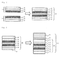
- Figure 1 is a diagrammatic illustration showing that two laminate films 1 are stuck to each other using adhesive to form a composite film 6, wherein 1 represents a laminate film, 2 represents a substrate film, 3 represents an organic layer, and 4 represents an inorganic layer.
- the two laminate films are provided so that the sides in which the inorganic layer is provided face each other through an adhesive layer 5.
- the substrate of the laminate film is thin, warpage tends to occur in the laminate film during the coating or depositing.
- the composite film is preferable since the laminate film balances the facing laminate film even if the warpage occurs.
- the inorganic layer surface in the laminate films can be protected.
- the adhesive layer is a layer comprising an adhesive as a main ingredient, and the adhesive generally occupies 70% by weight of the adhesive layer, preferably 80 to 90% by weight of the adhesive layer.
- Various known adhesives may be used as the adhesive, and preferably a urethane series adhesive.
- the urethane series adhesive is exemplified by a thermal curing adhesive and a UV curing adhesive. In the case where the laminate film absorbs UV, the thermal curing adhesive is preferable.
- the thermal curing adhesive includes one liquid type and two liquids type, and both types are preferably used in the invention. In the invention, an adhesive which becomes transparent after curing is preferable.
- Examples of the commercial adhesive include Seika bond E series manufactured by Dainichiseika Color & Chemicals and DICDRY LX series manufactured by DIC.
- a silane coupling agent is preferably added into the adhesive. By adding the silane coupling agent, the adhesion force is effectively enhanced.
- additives such as an ultraviolet absorber, a light stabilizer, an inorganic filler and a colorant may be added to extent that the adhesive property is not changed.
- the adhesive layer is formed by coating the adhesive by a coating method such as a roll coating method, a gravure coating method, a kiss coating method, a bar coating method and other known coating methods.
- the laminate film and the composite film of the invention may have a functional layer on the barrier layer or the like without diverting the scope of the invention.
- the functional layer is described in detail in JP-A 2006-289627 , paragraphs 0036 to 0038.
- Examples of other functional layers than those include a matting agent layer, a protective layer, a solvent resistance layer, an antistatic layer, a planarizing layer, an adhesiveness improving layer, a light shielding layer, an antireflection layer, a hard coat layer, a stress relaxing layer, an antifogging layer, an anti-soiling layer, a printable layer, an easy adhesive layer, etc.
- the laminate film and the composite film of the invention can be used for a sheet for solar cell devices.
- the sheet for solar cell devices may be a front sheet or back sheet, and preferably is a back sheet.
- Figure 2 is a diagrammatic illustration showing an example in which the composite film of the invention is applied to a back sheet of a solar cell device, wherein 6 shows the composite film and 7 shows the back sheet for a solar cell.
- the upper side corresponds to the upper side of the solar cell and the down side corresponds to the down side of the solar cell.
- the substrate film 2 which is at the upper side of the composite film 6 may optionally be stuck to a plastic film 9 with an adhesive layer 8.
- the substrate film 2 includes white pigment and, in order to enhance the insulation property to the substrate film, the plastic film 9 as a transparent film is adhered to the substrate film 2.
- the plastic film 9 adheres to the substrate film in the embodiment, however, it may be possible to omit the plastic film 9 by increasing the thickness of the substrate film 2 and adding a colorant into the substrate film.
- the embodiment in which the substrate film includes a colorant is preferably exemplified.
- the substrate film 2 which is used for a part corresponding to the back side of the solar cell preferably has weatherability, or the substrate film 2 may adhere to a film comprising a resin having weatherability, such as polyvinyl fluoride for the purpose of improving the weatherability of the substrate film 2.
- a resin having weatherability such as polyvinyl fluoride
- a solar cell device is provided between a back sheet such as mentioned above and a front sheet for a solar cell.
- the solar cell devices preferably applicable to the back sheet of the invention are not specifically limited.
- they include single crystal silicon-based solar cell devices, polycrystalline silicon-based solar cell devices, single-junction or tandem-structure amorphous silicon-based solar cell devices, gallium-arsenic (GaAs), indium-phosphorus (InP) or the like III-V Group compound semiconductor-based solar cell devices, cadmium-tellurium (CdTe) or the like II-VI Group compound semiconductor-based solar cell devices, copper/indium/selenium (CIS-based), copper/indium/gallium/selenium (CIGS-based), copper/indium/gallium/selenium/sulfur (CIGSS-based) or the like I-III-VI Group compound semiconductor-based solar cell devices, dye-sensitized solar cell devices, organic solar cell devices, etc.
- the solar cell devices are preferably copper/indium/selenium (CIS-based), copper/indium/gallium/selenium (CIGS-based), copper/indium/gallium/selenium/sulfur (CIGSS-based) or the like I-III-VI Group compound semiconductor-based solar cell devices.
- PET film having thickness of 12 ⁇ m, Rumilar S10 manufactured by TORAY
- an organic layer and an inorganic layer were formed in the following procedure.
- the obtained laminate film was measured and evaluated.
- a polymerizable composition consisting of 18 parts by weight of the polymerizable compounds having a composition shown in the following table (one of Compound A, Compound B and Compound C), 2 parts by weight of silane coupling agent (Compound S), 0.6 parts by weight of UV initiator (Ezacure KTO46 manufactured by Lambertis), and 190 parts by weight of 2-butanone was coated by bar coating method, and then put into a chamber having an oxygen concentration of 0.1% after nitrogen substitution, and the organic layer was cured therein through irradiation with UV light from a high-pressure mercury lamp (integrated radiation, about 1 J/cm 2 ), thereby constructing an organic layer having a thickness of 300 to 2500 nm ⁇ 50 nm.
- a high-pressure mercury lamp integrated radiation, about 1 J/cm 2
- an inorganic layer (silicon oxide) was formed on the surface of the organic layer.
- SiO as a depositing material
- the silicon oxide layer was formed by EB deposition method in which irradiation of electric beam is carried out by electron gun.
- the formation pressure was 0.003 Pa.
- the inorganic layer was formed on the surface of the organic layer to form a laminate film.
- Apparatus scanning atomic force microscope (AFM) (manufactured by Seiko Instruments Inc., type: SPI-3800N)
- the smoothness was measured and evaluated by the following; an arithmetic average roughness on a surface having 100 ⁇ m 2 to be measured: Ra (100 ⁇ m 2 ), and a ten-point average roughness on a surface having 100 ⁇ m 2 to be measured: Rz (100 ⁇ m 2 ).
- the smoothness of the surface of the organic layer as formed above was measured using an atom force microscope.
- the measurement for 100 ⁇ m 2 was carried out according to the above condition.
- the measurement for 10 ⁇ m 2 was carried out according to the above condition except that the area was changed to 10000 nm.
- the measurement was carried out at five-points on the same face and the average thereof was calculated.
- the smoothness was measured and evaluated by the following; an arithmetic average roughness on a surface having 10 ⁇ m 2 to be measured : Ra (10 ⁇ m 2 ), an arithmetic average roughness on a surface having 100 ⁇ m 2 to be measured : Ra (100 ⁇ m 2 ), and a ten-point average roughness on a surface having 100 ⁇ m 2 to be measured: Rz (100 ⁇ m 2 ).
- the water permeability (g/m 2 /day) was measured. The measurement was carried out at 40°C and at the relative humidity of 90%.
- Each of the laminate films consisting of the PET film, the organic layer on the PET film, and the inorganic layer on the organic film was transferred by roll to roll processing, and then, confirmed whether wrinkle occurred or not.
- the occurrence was shown as o and the non-occurrence was shown as ⁇ .
- Each of multilayered-laminate films was formed by the same method as the above 1, except that two of the organic layers and two of the inorganic layers were formed. It was found that the barrier property of those multilayered-laminate films was improved compared with that corresponding to the laminate films as formed in the above 1, respectively.
- each of solar cell modules was manufactured.
- As filler for a solar cell module standard cure type of ethylene-vinyl acetate copolymer was used.
- a solar cell of amorphous series silicone was sandwiched by ethylene-vinyl acetate copolymer films having a thickness of 450 ⁇ m, and then, on the surface thereof, the above laminate film was provided to form a solar cell module.
- the solar cell module was set up by vacuuming it at 150°C for 3 minutes and pressuring it for 9 minutes.
- the solar cell module as formed by the method worked properly and kept good electric generating power property even if used at 85°C and 85% RH.
- the laminate film of the invention is excellent in barrier property and is easy to be formed since it can be formed by roll to roll processing.
- the laminate film of the invention is preferably used for a sheet for a solar cell, especially as a back sheet for a solar cell.
Landscapes
- Chemical & Material Sciences (AREA)
- Health & Medical Sciences (AREA)
- Chemical Kinetics & Catalysis (AREA)
- Medicinal Chemistry (AREA)
- Polymers & Plastics (AREA)
- Organic Chemistry (AREA)
- Inorganic Chemistry (AREA)
- Laminated Bodies (AREA)
- Photovoltaic Devices (AREA)
Abstract
Description
- The invention relates to a laminate film. The invention also relates to a composite film obtained by adhering to the laminate films to each other. In particular, the invention relates to a film preferably used for a back sheet of a solar cell.
- In recent years, a solar energy generation system is prevailing as a way of generating electricity utilizing clean energy. Solar cell modules are generally composed of three layers of a glass, a cell for a solar cell (a semiconductor cell) and a back sheet.
- The back sheet protects the cell so as to avoid the degradation of the cell, thereby serving to maintain its generating efficiency. Such a back sheet is requested to have excellent mechanical property, heat resistance, and weatherability.
JP-A 2002-26354 JP-A-2003-60218 - Solar cells are requested to have high barrier property since those are put in outdoors for long years. As a result, it is investigated to use a laminate film in which an organic layer and an inorganic layer are laminated on a substrate film. In order to produce such a laminate film at low cost, a roll to roll processing which can produce a large-area film at high speed is chosen. When the laminate film is produced by the roll to roll processing, its important factor is its friction and slidability between a substrate film and a pass roller in transferring the substrate film at high speed, or its friction and slidability of laminated layers. That is, the film must be optimized in slidability. When the laminate film is poor in slidability, wrinkle often occurs in transferring or taking-up the film, and therefore, the slidability is highly demanded.
-
JP-A-2000-85067 JP-A-6-340046 - The inventor has investigated the film disclosed in
JP-A-2000-85067 JP-A-2000-85067 JP-A-6-340046 - An object of the invention is to solve the above problems, and is to provide a laminate film which has slidability and sufficient barrier property and which is used for a back sheet of a solar cell.
- In order to ensure slidability of a film, it is generally known that fine particles which are called as a matting agent are added into the film. Such a film comprising fine particles, however, has a rough surface. When an inorganic layer is formed on such a rough surface thereof, the inorganic layer becomes to have less denseness, which leads to decreased barrier property. Therefore, in general, an organic layer is formed on a rough surface thereof in order to smooth the surface. When such an organic layer is formed, the inorganic layer formed thereon becomes dense, thereby improving the barrier property of the laminate film. However, the slidability of the laminate film decreases.
- Under such situation, it has been found out that a laminate film which comprises a substrate film, an organic layer and an inorganic layer in that order, which has a dense inorganic layer, and which has a desired slidability can be formed by providing large wave on a surface of the organic layer and removing small wave from the surface of the organic layer. Specifically, the above problems have been solved by adjusting a surface of the organic layer to satisfy prescribed Ra and Rz and adjusting the thickness of the organic layer to have a prescribed thickness. Therefore, the invention has been completed.
- Specifically, the aforementioned problem can be solved by the following means.
- (1) A laminate film comprising a substrate film, an organic layer and an inorganic layer in that order, wherein the organic layer has a thickness of 300 nm to 2000 nm, the inorganic layer comprises silicon oxide represented by SiOx, wherein x is in a range from 0.9 to 1.5, and the organic layer has a surface satisfying all the following formulae;


- (2) The laminate film according to (1), wherein the substrate film has a surface satisfying all the following formulae;


300 nm < Rz(100 µm2) < 1200 nm. - (3) The laminate film according to (1) or (2), wherein the organic layer is obtained by curing a polymerizable composition comprising a (meth)acrylate.
- (4) The laminate film according to (1) or (2), wherein the organic layer is obtained by curing a polymerizable composition comprising a polyfunctional (meth)acrylate.
- (5) The laminate film according to (1) or (2), wherein the organic layer is obtained by curing a polymerizable composition comprising a polyfunctional (meth)acrylate having an aromatic carbon skeleton.
- (6) The laminate film according to any one of (1) to (5), wherein the substrate film comprises fine particles dispersed therein.
- (7) The laminate film according to (6), wherein the fine particles comprise one or more kinds selected from silicon oxide, titanium oxide and zirconium oxide.
- (8) The laminate film according to (6), wherein the fine particles comprise carbon black.
- (9) The laminate film according to any one of (1) to (8), wherein the substrate film comprises a colorant.
- (10) The laminate film according to any one of (1) to (9), wherein the organic layer comprises a silane coupling agent.
- (11) The laminate film according to any one of (1) to (10), wherein the inorganic layer comprises silicon oxide and/or aluminium oxide.
- (12) The laminate film according to any one of (1) to (11), wherein the inorganic layer is a layer formed by a vacuum deposition method.
(12-2) The laminate film according to any one of (1) to (12), wherein the inorganic layer is a layer formed by a plasma-assisted deposition method. - (13) A composite film comprising two laminate films, wherein the two laminate films each are the laminate film according to any one of (1) to (12-2) and adhere to each other at a side of its inorganic layer.
- (14) A back sheet for a solar cell comprising the laminate film according to any one of (1) to (12-2) or the composite film according to (13).
- (15) A method for producing a laminate film according to any one of (1) to (12-2), comprising transferring the substrate film by roll to roll processing.
- The invention makes it possible to provide a laminate film having slidability and sufficient barrier property.
-
-
Fig. 1 is a diagrammatic illustration showing that two laminate films are stuck together to form a composite film, wherein 1 is a laminate film, 2 is a substrate film, 3 is an organic layer, 4 is an inorganic layer, 5 is an adhesive layer, and 6 is a composite film. -
Fig. 2 is a diagrammatic illustration showing an example applying the composite film to a back sheet for a solar cell, wherein 7 is a back sheet for a solar cell, 8 is an adhesive layer and 9 is a plastic film. - The contents of the invention are described in detail hereinunder. In this description, the numerical range expressed by the wording "a number to another number" means the range that falls between the former number indicating the lowermost limit of the range and the latter number indicating the uppermost limit thereof. "Organic EL device" as referred to herein means an organic electroluminescent device. In addition, "(meth)acrylate" means acrylate and methacrylate in the present specification.
- The laminate film of the invention comprises a substrate film, an organic layer and an inorganic layer in that order, wherein the organic layer has a thickness of 300 nm to 2000 nm, the organic layer has a surface satisfying all the following formulae, and the inorganic layer comprises a silicon oxide represented by SiOx, wherein x is in a range from 0.9 to 1.5;


- By setting the surface of the organic layer to satisfy the above, occurrence of wrinkle and coil tightness in the laminate film are effectively reduced and high barrier property of the laminate film is achieved, even if the laminate film is transferred by roll to roll processing.
- In the invention, the substrate film and the organic layer are generally adjacent to each other. In the invention, a surface of the organic layer adjacent to the inorganic layer preferably satisfies all the above formulae.
- Ra in the specification means arithmetic average roughness, which is obtained by measuring a standard length between a point of a roughness profile and a point of the mean line which is vertically-extended from the point of a roughness profile, and adding up absolute values of deviation of the lengths to calculate their average value. Rz in the specification means ten-point arithmetic average roughness, which is obtained by measuring a standard length between a point of a roughness profile and a point of the mean line which is vertically-extended from the point of a roughness profile, and adding up the following averages (1) and (2);
- (1) average value of absolute values of heights from the highest peak to the fifth highest peak;
- (2) average value of absolute values of heights from the lowest valleys to the fifth lowest valleys.
- The surface of the organic layer preferably satisfies each of the following formulae;



- Furthermore, in the invention, the surface of the substrate film preferably satisfies all the following formulae in the invention;


- By setting the surface of the substrate film to satisfy the above, occurrence of wrinkle and coil tightness of the laminate film are effectively reduced even if the laminate film is produced by roll to roll processing.
- The surface of the substrate film further more preferably satisfies each of the following formulae;


- The organic layer of the invention is not specifically limited without deviating the scope of the invention, and is preferably a layer obtained by curing a polymerizable composition comprising a (meth)acrylate, more preferably a layer obtained by curing a polymerizable composition comprising a polyfunctional (meth)acrylate, further more preferably a layer obtained by curing a polymerizable composition comprising a polyfunctional (meth)acrylate having an aromatic carbon skeleton. Using a (meth)acrylate having an aromatic carbon skeleton is preferable since that tends to improve coatability of the substrate film and to improve the barrier property of the laminate film.
- Examples of the aromatic carbon skeleton include benzene skeleton, biphenyl skeleton, naphthalene skeleton, binaphthyl skeleton, azulene skeleton, biphenylene skeleton, acenaphthylene skeleton, phenanthrene skeleton, anthracene skeleton, triphenylene skeleton, pyrene skeleton, chrysene skeleton, naphthacene skeleton, picene skeleton, perylene skeleton, and benzopyrene skeleton.
- The aromatic carbon skeleton in the invention preferably has one or more aromatic rings, more preferably two or more aromatic rings. By employing a resin comprising an aromatic carbon skeleton having one or more aromatic rings, a layer which is more resistant to decomposition during plasma process can be formed. As a result, the barrier property of the laminate tends to be improved.
- Also, the resin in the organic layer in the invention is preferably a resin having a three dimension cross-linking performance. Use of such a resin makes a denser organic layer.
- The (meth) acrylates preferably used in the invention are exemplified below, to which, however, the invention is not limited thereto.


- The organic layer in the invention is preferably obtained by curing a polymerizable composition comprising a polymerizable compound as mentioned above and a polymerization initiator. In the polymerizable composition, the content of a (meth)acrylate having an aromatic carbon skeleton in the polymerizable compound ingredient is preferably 50 to 100% by weight.
- The polymerizable composition may comprise another polymerizable monomer in addition to the above polymerizable compounds without diverting the scope of the invention. The other polymerizable monomer is exemplified by a (meth) acrylate not having an aromatic carbon skeleton.
- The organic layer preferably comprises a silane coupling agent. Use of the silane coupling agent improves adhesiveness between the substrate film and the organic layer and adhesiveness between the organic layer and the inorganic layer, and therefore, it is possible to reduce degradation of the barrier property based on peeling failure. The amount of the silane coupling agent to be added in the organic layer is preferably 5 to 30% by weight, more preferably 10 to 25% by weight. By adjusting such a range, both of the high barrier property and the excellent adhesiveness are achieved. The silane coupling agent used in the invention is not particularly limited, and it is exemplified by KBM-5103 manufactured by Shin-Etsu Chemical.
- In the case where a photopolymerization initiator is used in the invention, its amount is preferably at least 0.1 mol% of the total amount of the polymerizing compound, more preferably from 0.5 to 2 mol%. By setting the thus-designed composition, polymerization reaction though an active ingredient forming reaction may be suitably controlled. Examples of the photopolymerization initiator include Ciba Speciality Chemicals' commercial products, Irgacure series (e.g., Irgacure 651, Irgacure 754, Irgacure 184, Irgacure 2959, Irgacure 907, Irgacure 369, Irgacure 379, Irgacure 819), Darocure series (e.g., Darocure TPO, Darocure 1173), Quantacure PDO; Lamberti's commercial products, Ezacure series (e.g., Ezacure TZM, Ezacure TZT, Ezacure KTO46), etc.
- The forming method of the organic layer is not specifically limited, and however, it is exemplified by a solution coating method or a vacuum film forming method.
- In the invention, the composition comprising the polymerizable monomer is generally cured by irradiation. The light for irradiation is generally a UV ray from a high-pressure mercury lamp or low-pressure mercury lamp. The radiation energy is preferably at least 0.1 J/cm2, more preferably at least 0.5 J/cm2. (Meth)acrylate series compounds used in the invention may suffer from interference in polymerization owing to oxygen in air, and therefore, in their polymerization, the oxygen concentration or the oxygen partial pressure is preferably lowered. In the case where the oxygen concentration in polymerization is lowered according to a nitrogen purging method, the oxygen concentration is preferably not more than 2 %, more preferably not more than 0.5 %. In the case where the oxygen partial pressure in polymerization is lowered by a pressure reduction method, the whole pressure is preferably not more than 1000 Pa, more preferably not more than 100 Pa. Especially preferred is UV polymerization with at least 0.5 J/cm2 energy radiation under a condition of reduced pressure of not more than 100 Pa.
- The thickness of the organic layer in the laminate film of the invention is 300 nm to 2000 nm, preferably 500 to 1500 nm, more preferably 750 to 1250 nm. By adjusting such a range, the optimal surface for the organic layer achieving high barrier property and appropriate slidability is obtained.
- In the laminate film of the invention, the substrate film is generally a plastic film. Not specifically defined in point of the material and the thickness thereof, the plastic film usable herein may be any one capable of supporting a laminate film of an organic layer and an inorganic layer; and it may be suitably selected depending on the use and the object thereof. Concretely, the plastic film includes thermoplastic resins such as polyester resin, methacryl resin, methacrylic acid-maleic anhydride copolymer, polystyrene resin, transparent fluororesin, polyimide, fluoropolyimide resin, polyamide resin, polyamidimide resin, polyetherimide resin, cellulose acylate resin, polyurethane resin, polyether ether ketone resin, polycarbonate resin, alicyclic polyolefin resin, polyarylate resin, polyether sulfone resin, polysulfone resin, cycloolefin copolymer, fluorene ring-modified polycarbonate resin, alicyclic-modified polycarbonate resin, fluorene ring-modified polyester resin, acryloyl compound.
- In case where the laminate film of the invention is used for an application requesting heat-resistance, it is desirable that the plastic film is formed of a heat-resistant material. Concretely, the plastic film is preferably formed of a heat-resistant transparent material having a glass transition temperature (Tg) of not lower than 100°C and/or a linear thermal expansion coefficient of not less than 40 ppm/°C. Tg and the linear expansion coefficient may be controlled by the additives to the material. The thermoplastic resin of the type includes, for example, polyethylene naphthalate (PEN: 120°C), polycarbonate (PC: 140°C), alicyclic polyolefin (e.g., Nippon Zeon's Zeonoa 1600: 160°C), polyarylate (PAr: 210°C), polyether sulfone (PES: 220°C), polysulfone (PSF: 190°C), cycloolefin copolymer (COC, compound described in
JP-A 2001-150584 JP-A 2000-227603 JP-A 2000-227603 JP-A 2002-80616 - The thickness of the substrate film used in the invention is appropriately chosen depending on its use and is not specifically limited. In the invention, may be used a thin film having a thickness of about 1 to 25 µm or a thick film having a thickness of about 30 to 300 µm.
- In the substrate film in the invention, fine particles as a matting agent may be dispersed. The film satisfying Ra and Rz as above-mentioned is readily obtained by having the fine particles dispersed thereon. Examples of such fine particles include silicon oxide, titanium oxide and zirconium oxide, and preferable is silicon oxide. Particularly, the substrate film having silicon oxide dispersed improves the coatability in the case of using the polymerizable composition comprising the above mentioned polyfunctional (meth)acrylate having an aromatic carbon skeleton.
- The substrate film in the invention may comprise fine particles in addition to the above fine particles as a colorant or as an agent combining a colorant and a matting agent. Examples thereof include carbon black and titanium oxide. By adding the colorant into the substrate film, the substrate film can be used as the outermost layer of the back sheet of a solar cell.
- The inorganic layer is, in general, a layer of a thin film formed of a metal compound. The inorganic layer is preferably formed by a vacuum deposition method or a plasma assisted-deposition method, and more preferably a vacuum deposition method. The plasma assisted-deposition method includes a method comprising ionizing a material to be deposited by plasma to carry out the deposition, or a method comprising irradiating gas ion from an ion source which is separately provided. By forming the inorganic layer by such methods, it makes possible to form a dense film at high speed.
- The inorganic layer in the invention comprises silicon oxide represented by SiOx, wherein x is in a range from 0.9 to 1.5, preferably in a range from 1.1 to 1.3. Using of such silicon oxide in wrapping material or optical material tended to be avoided since the film to be formed becomes ginger. However, when such silicon oxide is used in the invention, it has been found that high barrier property is achieved. The other component to be added in the inorganic layer is not specifically defined without diverting the scope of the invention, however, it is exemplified by metal oxide, metal nitride, metal carbide, metal oxynitride and metal oxycarbide. Preferably it is oxide, nitride, carbide, oxynitride or oxycarbide comprising one or more kinds of metals selected from Al, In, Sn, Zn, Ti, Cu, Ce and Ta. Of those, oxide, nitride or oxynitride of a metal selected from Al, In, Sn, Zn and Ti is preferable, oxide, nitride or oxynitride of Al is more preferable, and oxide of Al is further more preferable. The inorganic layer may contain another element in addition to the above elements as a subsidiary element.
- The surface of the inorganic layer preferably satisfies each of the following formulae;


- It is desirable that the inorganic layer is formed in a clean room. Preferably, the degree of cleanness is not more than class 10000, more preferably not more than class 1000.
- Not specifically defined, the thickness of the inorganic layer is generally within a range of from 5 to 500 nm/layer, preferably from 10 to 200 nm/layer. The inorganic layer may be a laminate composed of a plurality of sub-layers. In this case, each sub-layer may have the same composition, or a different composition.
- On the inorganic layer, a protective layer such as an overcoat layer may be provided.
- The inorganic layer may be provided on one side of the substrate film, or may be provided on the both sides of the substrate film. In addition, in the case where metal oxide and/or non-metal inorganic oxide which are used for the deposition are used as a mixture of two or more kinds thereof, the deposited film composed of different components can be formed.
- While the laminate film of the invention may be used as it is, the laminate film of the invention is preferably used as a composite film in which two of the laminate films are stuck to each other with an adhesive layer so that the sides in which the inorganic layer is provided face each other. In the case of laminating them, the laminate films are stuck together by known laminating methods such as a dry laminate method, an extrusion laminate method, and a thermal lamination method. Hereinafter, the composite film is described in detail.
Figure 1 is a diagrammatic illustration showing that twolaminate films 1 are stuck to each other using adhesive to form acomposite film 6, wherein 1 represents a laminate film, 2 represents a substrate film, 3 represents an organic layer, and 4 represents an inorganic layer. The two laminate films are provided so that the sides in which the inorganic layer is provided face each other through an adhesive layer 5. When the substrate of the laminate film is thin, warpage tends to occur in the laminate film during the coating or depositing. However, the composite film is preferable since the laminate film balances the facing laminate film even if the warpage occurs. In addition, the inorganic layer surface in the laminate films can be protected. - The adhesive layer is a layer comprising an adhesive as a main ingredient, and the adhesive generally occupies 70% by weight of the adhesive layer, preferably 80 to 90% by weight of the adhesive layer. Various known adhesives may be used as the adhesive, and preferably a urethane series adhesive. The urethane series adhesive is exemplified by a thermal curing adhesive and a UV curing adhesive. In the case where the laminate film absorbs UV, the thermal curing adhesive is preferable. The thermal curing adhesive includes one liquid type and two liquids type, and both types are preferably used in the invention. In the invention, an adhesive which becomes transparent after curing is preferable. Examples of the commercial adhesive include Seika bond E series manufactured by Dainichiseika Color & Chemicals and DICDRY LX series manufactured by DIC. In addition, a silane coupling agent is preferably added into the adhesive. By adding the silane coupling agent, the adhesion force is effectively enhanced. Into the adhesive, additives such as an ultraviolet absorber, a light stabilizer, an inorganic filler and a colorant may be added to extent that the adhesive property is not changed. The adhesive layer is formed by coating the adhesive by a coating method such as a roll coating method, a gravure coating method, a kiss coating method, a bar coating method and other known coating methods.
- The laminate film and the composite film of the invention may have a functional layer on the barrier layer or the like without diverting the scope of the invention. The functional layer is described in detail in
JP-A 2006-289627 - Examples of other functional layers than those include a matting agent layer, a protective layer, a solvent resistance layer, an antistatic layer, a planarizing layer, an adhesiveness improving layer, a light shielding layer, an antireflection layer, a hard coat layer, a stress relaxing layer, an antifogging layer, an anti-soiling layer, a printable layer, an easy adhesive layer, etc.
- The laminate film and the composite film of the invention, especially the composite film, can be used for a sheet for solar cell devices. The sheet for solar cell devices may be a front sheet or back sheet, and preferably is a back sheet.
Figure 2 is a diagrammatic illustration showing an example in which the composite film of the invention is applied to a back sheet of a solar cell device, wherein 6 shows the composite film and 7 shows the back sheet for a solar cell. In the back sheet for a solar cell 7, the upper side corresponds to the upper side of the solar cell and the down side corresponds to the down side of the solar cell. Thesubstrate film 2 which is at the upper side of thecomposite film 6 may optionally be stuck to aplastic film 9 with anadhesive layer 8. For example, it may be possible to form the embodiment wherein thesubstrate film 2 includes white pigment and, in order to enhance the insulation property to the substrate film, theplastic film 9 as a transparent film is adhered to thesubstrate film 2. Theplastic film 9 adheres to the substrate film in the embodiment, however, it may be possible to omit theplastic film 9 by increasing the thickness of thesubstrate film 2 and adding a colorant into the substrate film. Thus, the embodiment in which the substrate film includes a colorant is preferably exemplified. On the other hand, thesubstrate film 2 which is used for a part corresponding to the back side of the solar cell preferably has weatherability, or thesubstrate film 2 may adhere to a film comprising a resin having weatherability, such as polyvinyl fluoride for the purpose of improving the weatherability of thesubstrate film 2. - A solar cell device is provided between a back sheet such as mentioned above and a front sheet for a solar cell. The solar cell devices preferably applicable to the back sheet of the invention are not specifically limited. For example, they include single crystal silicon-based solar cell devices, polycrystalline silicon-based solar cell devices, single-junction or tandem-structure amorphous silicon-based solar cell devices, gallium-arsenic (GaAs), indium-phosphorus (InP) or the like III-V Group compound semiconductor-based solar cell devices, cadmium-tellurium (CdTe) or the like II-VI Group compound semiconductor-based solar cell devices, copper/indium/selenium (CIS-based), copper/indium/gallium/selenium (CIGS-based), copper/indium/gallium/selenium/sulfur (CIGSS-based) or the like I-III-VI Group compound semiconductor-based solar cell devices, dye-sensitized solar cell devices, organic solar cell devices, etc. Above all, in the invention, the solar cell devices are preferably copper/indium/selenium (CIS-based), copper/indium/gallium/selenium (CIGS-based), copper/indium/gallium/selenium/sulfur (CIGSS-based) or the like I-III-VI Group compound semiconductor-based solar cell devices.
- The characteristics of the invention are described more concretely with reference to the following Examples. In the following Examples, the material used, its amount and the ratio, the details of the treatment and the treatment process may be suitably modified or changed not overstepping the sprit and the scope of the invention. Accordingly, the invention should not be limitatively interpreted by the Examples mentioned below.
- On the surface of a polyethylene terephthalate film (PET film, having thickness of 12 µm, Rumilar S10 manufactured by TORAY), an organic layer and an inorganic layer were formed in the following procedure. The obtained laminate film was measured and evaluated.
- On the surface of the PET film, a polymerizable composition consisting of 18 parts by weight of the polymerizable compounds having a composition shown in the following table (one of Compound A, Compound B and Compound C), 2 parts by weight of silane coupling agent (Compound S), 0.6 parts by weight of UV initiator (Ezacure KTO46 manufactured by Lambertis), and 190 parts by weight of 2-butanone was coated by bar coating method, and then put into a chamber having an oxygen concentration of 0.1% after nitrogen substitution, and the organic layer was cured therein through irradiation with UV light from a high-pressure mercury lamp (integrated radiation, about 1 J/cm2), thereby constructing an organic layer having a thickness of 300 to 2500 nm ± 50 nm.
- Using a vacuum deposition apparatus, an inorganic layer (silicon oxide) was formed on the surface of the organic layer. Using SiO as a depositing material, the silicon oxide layer was formed by EB deposition method in which irradiation of electric beam is carried out by electron gun. The formation pressure was 0.003 Pa. The thickness was 80 nm. It was found to be SiOx(X=1.1) from the results of XPS measurement. Thus, the inorganic layer was formed on the surface of the organic layer to form a laminate film. Concerning Comparative 4, it was prepared so as to be x=1.7.
- The characteristic value of the obtained laminate films (Smoothness (Ra and Rz) and Waver vapor permeability) are shown in the following Tables 1 and 2.
- Using an atom force microscope, the Smoothness of the PET film used in the above was measured. The measurement was followed by the following conditions, and repeated five times on the same face to calculate an average value thereof.
- Apparatus: scanning atomic force microscope (AFM) (manufactured by Seiko Instruments Inc., type: SPI-3800N)
- Scanning frequency: 1.00Hz
- Area: 100000 nm
- The number of X data: 256
- The number of Y data: 256
- The smoothness was measured and evaluated by the following; an arithmetic average roughness on a surface having 100 µm2 to be measured: Ra (100 µm2), and
a ten-point average roughness on a surface having 100 µm2 to be measured: Rz (100 µm2). - The smoothness of the surface of the organic layer as formed above was measured using an atom force microscope. The measurement for 100 µm2 was carried out according to the above condition. The measurement for 10 µm2 was carried out according to the above condition except that the area was changed to 10000 nm. The measurement was carried out at five-points on the same face and the average thereof was calculated. The smoothness was measured and evaluated by the following;
an arithmetic average roughness on a surface having 10 µm2 to be measured : Ra (10 µm2),
an arithmetic average roughness on a surface having 100 µm2 to be measured : Ra (100 µm2), and
a ten-point average roughness on a surface having 100 µm2 to be measured: Rz (100 µm2). - Using a water vapor permeability apparatus (manufactured by MOCON, PERMATRAN-MR3/33 series G type), the water permeability (g/m2/day) was measured. The measurement was carried out at 40°C and at the relative humidity of 90%.
- Each of the laminate films consisting of the PET film, the organic layer on the PET film, and the inorganic layer on the organic film was transferred by roll to roll processing, and then, confirmed whether wrinkle occurred or not. The occurrence was shown as o and the non-occurrence was shown as ×.


- The compounds used above are as follows; Compound A:

- Compound B: Light acrylate TMP-A manufactured by Kyoeisha Chemical Co.,
- Compound C: Bisphenol A type epoxy acrylate, VR-60 (manufactured by Showa Highpolymer Co., LTD.)
- Compound S: KBM5103 manufactured by Shin-Etsu
- As is clear from the above tables, all of the laminate films of the invention have the vapor water permeability of 0.005g/m2/day or less. Each of the inorganic layers of the invention attained high smoothness. It was found that superior barrier property was attained by using a bifunctional (meth)acrylate having an polycyclic aromatic skeleton as a material of the organic layer. 2. Formation of Multilayered-laminate Film.
- Each of multilayered-laminate films was formed by the same method as the above 1, except that two of the organic layers and two of the inorganic layers were formed. It was found that the barrier property of those multilayered-laminate films was improved compared with that corresponding to the laminate films as formed in the above 1, respectively.
- Two of the laminate films as formed in the above 1 were adhered to each other so that the inorganic layers face inside, to thereby form a composite film. It was found that the barrier property of those composite films was further improved compared with that of the corresponding single laminate films, respectively.
- Using the laminate films as formed in the above 1, each of solar cell modules was manufactured. As filler for a solar cell module, standard cure type of ethylene-vinyl acetate copolymer was used. On the surface of a strengthen glass having a 10 cm2, a solar cell of amorphous series silicone was sandwiched by ethylene-vinyl acetate copolymer films having a thickness of 450 µm, and then, on the surface thereof, the above laminate film was provided to form a solar cell module. The solar cell module was set up by vacuuming it at 150°C for 3 minutes and pressuring it for 9 minutes. The solar cell module as formed by the method worked properly and kept good electric generating power property even if used at 85°C and 85% RH.
- The laminate film of the invention is excellent in barrier property and is easy to be formed since it can be formed by roll to roll processing. Thus, the laminate film of the invention is preferably used for a sheet for a solar cell, especially as a back sheet for a solar cell.
Claims (15)
- A laminate film comprising a substrate film, an organic layer and an inorganic layer in that order, wherein the organic layer has a thickness of 300 nm to 2000 nm, the inorganic layer comprises silicon oxide represented by SiOx, wherein x is in a range from 0.9 to 1.5, and the organic layer has a surface satisfying all the following formulae;


- The laminate film according to Claim 1, wherein the substrate film has a surface satisfying all the following formulae;
Ra(100 µm2) < 50 nm
300 nm < Rz(100 µm2) < 1200 nm. - The laminate film according to Claim 1 or 2, wherein the organic layer is obtained by curing a polymerizable composition comprising a (meth)acrylate.
- The laminate film according to Claim 1 or 2, wherein the organic layer is obtained by curing a polymerizable composition comprising a polyfunctional (meth)acrylate.
- The laminate film according to Claim 1 or 2, wherein the organic layer is obtained by curing a polymerizable composition comprising a polyfunctional (meth) acrylate having an aromatic carbon skeleton.
- The laminate film according to any one of Claims 1 to 5, wherein the substrate film comprises fine particles dispersed therein.
- The laminate film according to Claim 6, wherein the fine particles comprise one or more kinds selected from silicon oxide, titanium oxide and zirconium oxide.
- The laminate film according to Claim 6, wherein the fine particles comprise carbon black.
- The laminate film according to any one of Claims 1 to 8, wherein the substrate film comprises a colorant.
- The laminate film according to any one of Claims 1 to 9, wherein the organic layer comprises a silane coupling agent.
- The laminate film according to any one of Claims 1 to 10, wherein the inorganic layer comprises silicon oxide and/or aluminium oxide.
- The laminate film according to any one of Claims 1 to 11, wherein the inorganic layer is a layer formed by a vacuum deposition method.
- A composite film comprising two laminate films, wherein the two laminate films each are the laminate film according to any one of Claims 1 to 12 and adhere to each other at a side of its inorganic layer.
- A back sheet for a solar cell, comprising the laminate film according to any one of Claims 1 to 12 or the composite film according to Claim 13.
- A method for producing the laminate film according to any one of Claims 1 to 12, comprising transferring the substrate film by roll to roll processing.
Applications Claiming Priority (1)
| Application Number | Priority Date | Filing Date | Title |
|---|---|---|---|
| JP2009195234A JP5281986B2 (en) | 2009-08-26 | 2009-08-26 | Laminated film and composite film |
Publications (1)
| Publication Number | Publication Date |
|---|---|
| EP2289984A1 true EP2289984A1 (en) | 2011-03-02 |
Family
ID=42990338
Family Applications (1)
| Application Number | Title | Priority Date | Filing Date |
|---|---|---|---|
| EP10173974A Withdrawn EP2289984A1 (en) | 2009-08-26 | 2010-08-25 | Laminate film and composite film |
Country Status (5)
| Country | Link |
|---|---|
| US (1) | US8283020B2 (en) |
| EP (1) | EP2289984A1 (en) |
| JP (1) | JP5281986B2 (en) |
| KR (1) | KR101730654B1 (en) |
| CN (1) | CN102001201B (en) |
Families Citing this family (16)
| Publication number | Priority date | Publication date | Assignee | Title |
|---|---|---|---|---|
| TW201307468A (en) * | 2011-07-14 | 2013-02-16 | Fujifilm Corp | Polymer sheet and solar cell module for solar cells |
| JPWO2013031752A1 (en) * | 2011-08-30 | 2015-03-23 | 東レ株式会社 | Method for manufacturing solar cell module, solar cell back surface sealing sheet, and solar cell module |
| JP5752000B2 (en) * | 2011-09-26 | 2015-07-22 | 富士フイルム株式会社 | Barrier laminate, gas barrier film and device using the same |
| JP5763493B2 (en) * | 2011-09-30 | 2015-08-12 | 富士フイルム株式会社 | Barrier laminate, gas barrier film and device using the same |
| JP2013111507A (en) * | 2011-11-25 | 2013-06-10 | Fujifilm Corp | Gas separation membrane, method of manufacturing the same, and gas separation membrane module using the same |
| JP5812916B2 (en) * | 2012-03-29 | 2015-11-17 | 富士フイルム株式会社 | Barrier laminate, gas barrier film and device using the same |
| WO2013161894A1 (en) * | 2012-04-25 | 2013-10-31 | コニカミノルタ株式会社 | Gas barrier film, substrate for electronic device, and electronic device |
| CN102709368B (en) * | 2012-06-21 | 2015-06-17 | 宁波长阳科技有限公司 | Solar battery back board and preparation method thereof |
| EP3024883A1 (en) * | 2013-07-24 | 2016-06-01 | 3M Innovative Properties Company | Adhesive barrier film construction |
| JP6482977B2 (en) * | 2014-11-10 | 2019-03-13 | 住友化学株式会社 | Laminated film for flexible device, optical member, display member, front plate, and method for producing laminated film for flexible device |
| WO2016076243A1 (en) * | 2014-11-10 | 2016-05-19 | 住友化学株式会社 | Resin film, laminated film, optical member, display member, front plate, and method for producing laminated film |
| JP2017069290A (en) * | 2015-09-28 | 2017-04-06 | 日清紡メカトロニクス株式会社 | PID deterioration preventing solar cell module film and PID deterioration preventing solar cell module using the same |
| TW201829190A (en) * | 2016-11-11 | 2018-08-16 | 日商住友化學股份有限公司 | Gas barrier film and device including the same |
| JP6421401B1 (en) * | 2017-07-20 | 2018-11-14 | 東洋インキScホールディングス株式会社 | Active energy ray curable overcoat varnish |
| CN107316912B (en) * | 2017-08-11 | 2018-10-16 | 北京铂阳顶荣光伏科技有限公司 | The packaging method of roll-to-roll flexible photovoltaic component |
| CN113427839A (en) * | 2021-08-26 | 2021-09-24 | 金石(天津)科技发展有限公司 | Composite film bag and preparation method thereof |
Citations (9)
| Publication number | Priority date | Publication date | Assignee | Title |
|---|---|---|---|---|
| JPH06340046A (en) | 1993-06-01 | 1994-12-13 | Teijin Ltd | Laminated polyester film |
| JP2000085067A (en) | 1998-09-17 | 2000-03-28 | Mitsubishi Polyester Film Copp | Laminated polyester film for vapor deposition |
| JP2000227603A (en) | 1998-11-30 | 2000-08-15 | Teijin Ltd | Liquid crystal display device and transparent conductive substrate suitable therefor |
| JP2001150584A (en) | 1999-11-29 | 2001-06-05 | Nippon Zeon Co Ltd | Conductive substrate and display element using the same |
| JP2002026354A (en) | 2000-07-11 | 2002-01-25 | Toray Ind Inc | Solar cell backside sealing film and solar cell using the same |
| JP2002080616A (en) | 2000-06-30 | 2002-03-19 | Sumitomo Bakelite Co Ltd | Polymer film for display element and substrate for display element using the same |
| JP2003060218A (en) | 2001-08-21 | 2003-02-28 | Toray Ind Inc | Solar cell backside sealing film and solar cell using the same |
| JP2006248239A (en) * | 2006-05-24 | 2006-09-21 | Mitsubishi Plastics Ind Ltd | Deposition polyester film |
| JP2006289627A (en) | 2005-04-06 | 2006-10-26 | Fuji Photo Film Co Ltd | Gas barrier film and organic device using the same |
Family Cites Families (12)
| Publication number | Priority date | Publication date | Assignee | Title |
|---|---|---|---|---|
| EP0203604B1 (en) * | 1985-05-29 | 1990-08-22 | Teijin Limited | Polyester film for magnetic recording media |
| JP3271418B2 (en) * | 1994-03-03 | 2002-04-02 | 東洋紡績株式会社 | Gas barrier film and gas barrier film for retort |
| JP2003154596A (en) * | 2001-11-22 | 2003-05-27 | Nitto Denko Corp | Transparent gas barrier film, and transparent conductive electrode substrate, display element, solar cell or planar light-emitting body using the same |
| JP4254350B2 (en) * | 2002-12-16 | 2009-04-15 | 住友ベークライト株式会社 | Transparent barrier film |
| JP2005144719A (en) * | 2003-11-12 | 2005-06-09 | Reiko Co Ltd | Gas barrier composite film excellent in weatherability |
| US20050238846A1 (en) * | 2004-03-10 | 2005-10-27 | Fuji Photo Film Co., Ltd. | Gas barrier laminate film, method for producing the same and image display device utilizing the film |
| JP5214087B2 (en) * | 2004-05-06 | 2013-06-19 | 恵和株式会社 | Back sheet for solar cell module and solar cell module using the same |
| JPWO2007111076A1 (en) * | 2006-03-24 | 2009-08-06 | コニカミノルタエムジー株式会社 | Transparent barrier sheet and method for producing transparent barrier sheet |
| JP2009083465A (en) * | 2007-09-14 | 2009-04-23 | Fujifilm Corp | Gas barrier film and display element using the same |
| JP5262044B2 (en) * | 2007-09-27 | 2013-08-14 | 凸版印刷株式会社 | Solar cell back surface sealing sheet and solar cell module using the same |
| JP2010274562A (en) * | 2009-05-29 | 2010-12-09 | Fujifilm Corp | Gas barrier laminate and method for producing gas barrier laminate |
| JP5414426B2 (en) * | 2009-09-01 | 2014-02-12 | 富士フイルム株式会社 | Composite film |
-
2009
- 2009-08-26 JP JP2009195234A patent/JP5281986B2/en not_active Expired - Fee Related
-
2010
- 2010-08-24 US US12/862,396 patent/US8283020B2/en not_active Expired - Fee Related
- 2010-08-25 KR KR1020100082570A patent/KR101730654B1/en not_active Expired - Fee Related
- 2010-08-25 EP EP10173974A patent/EP2289984A1/en not_active Withdrawn
- 2010-08-25 CN CN201010261691.2A patent/CN102001201B/en not_active Expired - Fee Related
Patent Citations (9)
| Publication number | Priority date | Publication date | Assignee | Title |
|---|---|---|---|---|
| JPH06340046A (en) | 1993-06-01 | 1994-12-13 | Teijin Ltd | Laminated polyester film |
| JP2000085067A (en) | 1998-09-17 | 2000-03-28 | Mitsubishi Polyester Film Copp | Laminated polyester film for vapor deposition |
| JP2000227603A (en) | 1998-11-30 | 2000-08-15 | Teijin Ltd | Liquid crystal display device and transparent conductive substrate suitable therefor |
| JP2001150584A (en) | 1999-11-29 | 2001-06-05 | Nippon Zeon Co Ltd | Conductive substrate and display element using the same |
| JP2002080616A (en) | 2000-06-30 | 2002-03-19 | Sumitomo Bakelite Co Ltd | Polymer film for display element and substrate for display element using the same |
| JP2002026354A (en) | 2000-07-11 | 2002-01-25 | Toray Ind Inc | Solar cell backside sealing film and solar cell using the same |
| JP2003060218A (en) | 2001-08-21 | 2003-02-28 | Toray Ind Inc | Solar cell backside sealing film and solar cell using the same |
| JP2006289627A (en) | 2005-04-06 | 2006-10-26 | Fuji Photo Film Co Ltd | Gas barrier film and organic device using the same |
| JP2006248239A (en) * | 2006-05-24 | 2006-09-21 | Mitsubishi Plastics Ind Ltd | Deposition polyester film |
Non-Patent Citations (1)
| Title |
|---|
| DATABASE WPI Week 200668, Derwent World Patents Index; AN 2006-652000, XP002607504 * |
Also Published As
| Publication number | Publication date |
|---|---|
| KR101730654B1 (en) | 2017-04-26 |
| JP5281986B2 (en) | 2013-09-04 |
| JP2011046046A (en) | 2011-03-10 |
| CN102001201B (en) | 2015-03-18 |
| US8283020B2 (en) | 2012-10-09 |
| KR20110021694A (en) | 2011-03-04 |
| CN102001201A (en) | 2011-04-06 |
| US20110052868A1 (en) | 2011-03-03 |
Similar Documents
| Publication | Publication Date | Title |
|---|---|---|
| US8283020B2 (en) | Laminate film and composite film | |
| JP5414426B2 (en) | Composite film | |
| JP5216724B2 (en) | Gas barrier film and device | |
| EP2128191B1 (en) | Barrier laminate, gas barrier film, device, and method for producing barrier laminate | |
| EP2302695B1 (en) | Gas barrier composite, back sheet for solar cell module and solar cell module | |
| US20100003480A1 (en) | Barrier laminate, gas barrier film, device and optical member | |
| JP5334900B2 (en) | Gas barrier film and device | |
| WO2013027786A1 (en) | Barrier laminate, and gas barrier film | |
| JP2011200780A (en) | Barrier laminated body, method for manufacturing the same, gas barrier film, and device | |
| JP5580561B2 (en) | Barrier laminate, gas barrier film, and method for producing barrier laminate | |
| JP5712509B2 (en) | Barrier film manufacturing method | |
| CN109476138B (en) | Gas barrier film, solar cell, and method for producing gas barrier film | |
| JP5657297B2 (en) | Gas barrier film and electronic device | |
| US20090324978A1 (en) | Barrier laminate, gas barrier film and device | |
| WO2015030178A1 (en) | Barrier laminate, gas barrier film and device | |
| JP2012020409A (en) | Laminate with barrier property, gas barrier film, device using the laminate with barrier property and the gas barrier film and method of manufacturing the laminate with barrier property | |
| JP6237473B2 (en) | Method for producing gas barrier film | |
| WO2015119109A1 (en) | Production method for gas-barrier film, and gas-barrier film | |
| JP5823277B2 (en) | Barrier laminate, gas barrier film and device using the same | |
| JP6909780B2 (en) | Composite articles including multi-layer barrier assemblies and methods for their manufacture | |
| JP2000332277A (en) | Protection sheet for solar cell module and solar cell module using the same | |
| CN110114897B (en) | Electronic equipment | |
| JP2001196613A (en) | Solar cell module |
Legal Events
| Date | Code | Title | Description |
|---|---|---|---|
| PUAI | Public reference made under article 153(3) epc to a published international application that has entered the european phase |
Free format text: ORIGINAL CODE: 0009012 |
|
| AK | Designated contracting states |
Kind code of ref document: A1 Designated state(s): AL AT BE BG CH CY CZ DE DK EE ES FI FR GB GR HR HU IE IS IT LI LT LU LV MC MK MT NL NO PL PT RO SE SI SK SM TR |
|
| AX | Request for extension of the european patent |
Extension state: BA ME RS |
|
| 17P | Request for examination filed |
Effective date: 20110701 |
|
| 17Q | First examination report despatched |
Effective date: 20160301 |
|
| GRAP | Despatch of communication of intention to grant a patent |
Free format text: ORIGINAL CODE: EPIDOSNIGR1 |
|
| INTG | Intention to grant announced |
Effective date: 20181129 |
|
| STAA | Information on the status of an ep patent application or granted ep patent |
Free format text: STATUS: THE APPLICATION IS DEEMED TO BE WITHDRAWN |
|
| 18D | Application deemed to be withdrawn |
Effective date: 20190410 |