EP2287370A1 - A l X G a 1-X N SINGLE CRYSTAL AND ELECTROMAGNETIC WAVE TRANSMISSION BODY - Google Patents
A l X G a 1-X N SINGLE CRYSTAL AND ELECTROMAGNETIC WAVE TRANSMISSION BODY Download PDFInfo
- Publication number
- EP2287370A1 EP2287370A1 EP09754637A EP09754637A EP2287370A1 EP 2287370 A1 EP2287370 A1 EP 2287370A1 EP 09754637 A EP09754637 A EP 09754637A EP 09754637 A EP09754637 A EP 09754637A EP 2287370 A1 EP2287370 A1 EP 2287370A1
- Authority
- EP
- European Patent Office
- Prior art keywords
- single crystal
- electromagnetic wave
- wave transmission
- ain
- transmission body
- Prior art date
- Legal status (The legal status is an assumption and is not a legal conclusion. Google has not performed a legal analysis and makes no representation as to the accuracy of the status listed.)
- Withdrawn
Links
Images


Classifications
-
- C—CHEMISTRY; METALLURGY
- C30—CRYSTAL GROWTH
- C30B—SINGLE-CRYSTAL GROWTH; UNIDIRECTIONAL SOLIDIFICATION OF EUTECTIC MATERIAL OR UNIDIRECTIONAL DEMIXING OF EUTECTOID MATERIAL; REFINING BY ZONE-MELTING OF MATERIAL; PRODUCTION OF A HOMOGENEOUS POLYCRYSTALLINE MATERIAL WITH DEFINED STRUCTURE; SINGLE CRYSTALS OR HOMOGENEOUS POLYCRYSTALLINE MATERIAL WITH DEFINED STRUCTURE; AFTER-TREATMENT OF SINGLE CRYSTALS OR A HOMOGENEOUS POLYCRYSTALLINE MATERIAL WITH DEFINED STRUCTURE; APPARATUS THEREFOR
- C30B29/00—Single crystals or homogeneous polycrystalline material with defined structure characterised by the material or by their shape
- C30B29/10—Inorganic compounds or compositions
- C30B29/40—AIIIBV compounds wherein A is B, Al, Ga, In or Tl and B is N, P, As, Sb or Bi
- C30B29/403—AIII-nitrides
-
- C—CHEMISTRY; METALLURGY
- C30—CRYSTAL GROWTH
- C30B—SINGLE-CRYSTAL GROWTH; UNIDIRECTIONAL SOLIDIFICATION OF EUTECTIC MATERIAL OR UNIDIRECTIONAL DEMIXING OF EUTECTOID MATERIAL; REFINING BY ZONE-MELTING OF MATERIAL; PRODUCTION OF A HOMOGENEOUS POLYCRYSTALLINE MATERIAL WITH DEFINED STRUCTURE; SINGLE CRYSTALS OR HOMOGENEOUS POLYCRYSTALLINE MATERIAL WITH DEFINED STRUCTURE; AFTER-TREATMENT OF SINGLE CRYSTALS OR A HOMOGENEOUS POLYCRYSTALLINE MATERIAL WITH DEFINED STRUCTURE; APPARATUS THEREFOR
- C30B23/00—Single-crystal growth by condensing evaporated or sublimed materials
- C30B23/02—Epitaxial-layer growth
-
- C—CHEMISTRY; METALLURGY
- C30—CRYSTAL GROWTH
- C30B—SINGLE-CRYSTAL GROWTH; UNIDIRECTIONAL SOLIDIFICATION OF EUTECTIC MATERIAL OR UNIDIRECTIONAL DEMIXING OF EUTECTOID MATERIAL; REFINING BY ZONE-MELTING OF MATERIAL; PRODUCTION OF A HOMOGENEOUS POLYCRYSTALLINE MATERIAL WITH DEFINED STRUCTURE; SINGLE CRYSTALS OR HOMOGENEOUS POLYCRYSTALLINE MATERIAL WITH DEFINED STRUCTURE; AFTER-TREATMENT OF SINGLE CRYSTALS OR A HOMOGENEOUS POLYCRYSTALLINE MATERIAL WITH DEFINED STRUCTURE; APPARATUS THEREFOR
- C30B25/00—Single-crystal growth by chemical reaction of reactive gases, e.g. chemical vapour-deposition growth
- C30B25/02—Epitaxial-layer growth
-
- H—ELECTRICITY
- H10—SEMICONDUCTOR DEVICES; ELECTRIC SOLID-STATE DEVICES NOT OTHERWISE PROVIDED FOR
- H10P—GENERIC PROCESSES OR APPARATUS FOR THE MANUFACTURE OR TREATMENT OF DEVICES COVERED BY CLASS H10
- H10P14/00—Formation of materials, e.g. in the shape of layers or pillars
- H10P14/20—Formation of materials, e.g. in the shape of layers or pillars of semiconductor materials
- H10P14/22—Formation of materials, e.g. in the shape of layers or pillars of semiconductor materials using physical deposition, e.g. vacuum deposition or sputtering
-
- H—ELECTRICITY
- H10—SEMICONDUCTOR DEVICES; ELECTRIC SOLID-STATE DEVICES NOT OTHERWISE PROVIDED FOR
- H10P—GENERIC PROCESSES OR APPARATUS FOR THE MANUFACTURE OR TREATMENT OF DEVICES COVERED BY CLASS H10
- H10P14/00—Formation of materials, e.g. in the shape of layers or pillars
- H10P14/20—Formation of materials, e.g. in the shape of layers or pillars of semiconductor materials
- H10P14/29—Formation of materials, e.g. in the shape of layers or pillars of semiconductor materials characterised by the substrates
- H10P14/2901—Materials
- H10P14/2902—Materials being Group IVA materials
- H10P14/2904—Silicon carbide
-
- H—ELECTRICITY
- H10—SEMICONDUCTOR DEVICES; ELECTRIC SOLID-STATE DEVICES NOT OTHERWISE PROVIDED FOR
- H10P—GENERIC PROCESSES OR APPARATUS FOR THE MANUFACTURE OR TREATMENT OF DEVICES COVERED BY CLASS H10
- H10P14/00—Formation of materials, e.g. in the shape of layers or pillars
- H10P14/20—Formation of materials, e.g. in the shape of layers or pillars of semiconductor materials
- H10P14/34—Deposited materials, e.g. layers
- H10P14/3402—Deposited materials, e.g. layers characterised by the chemical composition
- H10P14/3414—Deposited materials, e.g. layers characterised by the chemical composition being group IIIA-VIA materials
- H10P14/3416—Nitrides
-
- Y—GENERAL TAGGING OF NEW TECHNOLOGICAL DEVELOPMENTS; GENERAL TAGGING OF CROSS-SECTIONAL TECHNOLOGIES SPANNING OVER SEVERAL SECTIONS OF THE IPC; TECHNICAL SUBJECTS COVERED BY FORMER USPC CROSS-REFERENCE ART COLLECTIONS [XRACs] AND DIGESTS
- Y10—TECHNICAL SUBJECTS COVERED BY FORMER USPC
- Y10T—TECHNICAL SUBJECTS COVERED BY FORMER US CLASSIFICATION
- Y10T428/00—Stock material or miscellaneous articles
- Y10T428/24—Structurally defined web or sheet [e.g., overall dimension, etc.]
- Y10T428/24355—Continuous and nonuniform or irregular surface on layer or component [e.g., roofing, etc.]
Definitions
- the present invention relates to Al x Ga 1-x N (0 ⁇ x ⁇ 1) single crystals and electromagnetic wave transmission bodies containing Al x Ga 1 -x N single crystals, suitably utilized in electronic components, microelectronic components, optoelectronic components, and like applications.
- electromagnetic wave transmission bodies In plasma generation apparatuses, which apply radio-frequency power to gases to create plasmas, materials such as quartz glass are employed as an electromagnetic wave transmission body. When exposed to a plasma of non-corrosive gases such as Ar, N 2 , O 2 or SiH 4 , such electromagnetic wave transmission bodies emit heat owing, in addition to absorption of the high-frequency energy, to ion bombardment and radiant heat from the plasma, therefore making necessary heat-emission prevention and heat-shock resistance in electromagnetic wave transmission bodies.
- non-corrosive gases such as Ar, N 2 , O 2 or SiH 4
- quartz glass as an electromagnetic wave transmission body is exposed to plasma from chlorine- or fluorine-containing corrosive gases corrosive gases such as C1F 3 , NF 3 , CF 4 , CHF 3 , and SiH 2 Cl 2 for example-a difficulty arises in that the material is etched at a high rate and Si and O, etching by-products from the quartz, mix into the plasma.
- corrosive gases such as C1F 3 , NF 3 , CF 4 , CHF 3 , and SiH 2 Cl 2
- Alumina (aluminum oxide) is effective from the standpoint of resistance to corrosive gases. However, because alumina has poor resistance to heat shock and has a low thermal conductivity, there is the problem of the temperature becoming locally high with a high-power plasma, and thermal stress causing breakage.
- an aluminum nitride sintered ceramic having a high thermal conductivity and a low thermal expansion coefficient has a high resistance to corrosive halogen-based gases, and is preferable to alumina (cf., for example, Japanese Unexamined Pat. App. Pub. H07-142197 (Patent Document 1) and Japanese Unexamined Pat. App. Pub. H07-142414 (Patent Document 2)).
- Patent Document 1 Japanese Unexamined Pat. App. Pub. H07-142197
- Patent Document 2 Japanese Unexamined Pat. App. Pub. H07-142414
- Patent Document 4 Japanese Unexamined Pat. App. Pub. No. 2006-08493 (Patent Document 5)
- Patent Document 5 Japanese Unexamined Pat. App. Pub. No. 2006-08493
- an aluminum nitride sinter has many crystal grain boundaries and often contains a sintering additive. For this reason, because an aluminum nitride sinter has low thermal conductivity compared to an aluminum nitride single crystal and the coefficient of thermal expansion thereof exhibits local variations, there is a limitation to the increase in resistance to heat shock.
- an aluminum nitride sinter Compared to aluminum nitride single crystals, an aluminum nitride sinter has many crystal defects, and because a sintering aide such as Al 2 O 3 , Y 2 O 5 , CaO, or MgO is used as a source material, the oxygen concentration is high. For this reason, an aluminum nitride sinter has a high dielectric loss tangent, and there is the problem that when high-power RF electrical power is applied, the temperature increases sharply and the dielectric properties change.
- a sintering aide such as Al 2 O 3 , Y 2 O 5 , CaO, or MgO
- an object of the present invention is to solve the above-noted problems and to make available an Al x Ga 1- x N single crystal suitable as an electromagnetic wave transmission body and an electromagnetic wave transmission body that includes the Al x Ga 1- x N single crystal.
- the present invention is an Al x Ga 1- x N (0 ⁇ x ⁇ 1) single crystal having a dielectric loss tangent of 5 ⁇ 10 -3 or lower when an RF signal of at least either 1 MHz or 1 GHz is applied to the crystal at an atmospheric temperature of 25°C.
- the Al x Ga 1- x N single crystal of the present invention can be made to have a dielectric loss tangent of 5 ⁇ 10 -3 or lower with a 1-MHz RF signal applied thereto and also made to have a dielectric loss tangent of 5 ⁇ 10 -3 or lower with a 1-GHz RF signal applied thereto.
- the oxygen concentration of the Al x Ga 1- x N single crystal of the present invention can be made 1 ⁇ 10 18 cm -3 or lower.
- the dislocation density of the Al x Ga 1- x N single crystal of the present invention can be made 1 ⁇ 10 6 cm -2 or lower.
- the span or diameter of the Al x Ga 1- x N single crystal of the present invention can be made 10 mm or greater and the thickness thereof can be made 300 ⁇ m or lower.
- the RMS surface roughness of the Al x Ga 1- x N single crystal can be made 100 nm or lower.
- the present invention is an electromagnetic wave transmission body that includes an Al x Ga 1- x N (0 ⁇ x ⁇ 1) single crystal having a major plane, wherein the dielectric loss tangent of the Al x Ga 1- x N single crystal is 5 ⁇ 10 -3 or lower with at least either a 1-MHz RF signal or a 1-GHz RF signal having been applied thereto at an atmospheric temperature of 25°C.
- the Al x Ga 1- x N single crystal can be made to have a dielectric loss tangent of 5 ⁇ 10 -3 or lower with a 1-MHz RF signal having been applied thereto and also to have a dielectric loss tangent of 5 ⁇ 10 -3 or lower with a 1-GHz RF signal having been applied thereto.
- the oxygen concentration of the Al x Ga 1- x N single crystal of the present invention can be made 1 ⁇ 10 18 cm -3 or lower.
- the dislocation density of the Al x Ga 1- x N single crystal of the present invention can be made 1 ⁇ 10 6 cm -2 or lower.
- the span or diameter of the Al x Ga 1- x N single crystal of the present invention can be made 10 mm or greater, and the thickness thereof can be made 300 ⁇ m or greater.
- the RMS surface roughness of the Al x Ga 1- x N single crystal can be made 100 nm or lower.
- the present invention make available an Al x Ga 1- x N single crystal preferable as an electromagnetic wave transmission body, as well as an electromagnetic wave transmission body that includes the Al x Ga 1- x N single crystal.
- the Al x Ga 1- x N single crystal that is the first embodying mode of the present invention has a high thermal conductivity, and little local variation in the coefficient of thermal expansion. For this reason, even if exposed to a high-frequency plasma, the Al x Ga 1- x N single crystal tends to be immune to thermal stress and has a high resistance to heat shock.
- the Al x Ga 1- x N single crystal of this embodying mode has a dielectric loss tangent of 5 ⁇ 10 -3 or lower when at least either a 1-MHz RF signal or a 1-GHz RF signal is applied thereto at an atmospheric temperature of 25°C, even if high-frequency electromagnetic radiation is transmitted, the dielectric losses are extremely small, making it suitable as an electromagnetic wave transmission body.
- the Al x Ga 1- x N single crystal of this embodying mode have a dielectric loss tangent of 5 ⁇ 10 -3 or lower when a 1-MHz RF signal is applied thereto and also a dielectric loss tangent of 5 ⁇ 10 -3 or lower when a 1-GHz RF signal is applied thereto.
- the Al x Ga 1- x N single crystal has an extremely low dielectric loss even when transmitting electromagnetic radiation over a broad range of high frequencies spanning from the order of MHz to the order of GHz, and is preferably used as an electromagnetic wave transmission body.
- oxygen atoms included in an Al x Ga 1- x N single crystal are replaced by nitrogen atoms (replacement oxygen atom ON), and also bond to lattice defects (vacancy V Al ) in the aluminum, so as to form a complex defect V Al -O N ). It is thought that the dielectric loss tangent becomes large by this complex defect V Al -O N forming a dipole.
- the Al x Ga 1- x N single crystal of this embodying mode although it is not particularly limited in this regard, has an oxygen concentration that is preferably 1 ⁇ 10 18 cm -3 or lower, and more preferably 3 ⁇ 10 17 cm -3 or lower.
- the Al x Ga 1- x N single crystal of this embodying mode although not particularly limited in this regard, has a dislocation density that is preferably 1 ⁇ 10 6 cm -2 or lower and more preferably 5 ⁇ 10 5 cm -2 or lower, and yet more preferably 1 ⁇ 10 5 cm -2 or lower.
- the Al x Ga 1- x N single crystal of this embodying mode has a span or diameter that is preferably 10 mm or greater and a thickness that is preferably 300 ⁇ m or greater.
- the span or diameter of the Al x Ga 1- x N single crystal is preferably 50 mm or greater and more preferably 100 mm or greater.
- the thickness of the Al x Ga 1- x N single crystal is preferably 300 ⁇ m or greater, more preferably 1000 ⁇ m or greater, and yet more preferably 3000 ⁇ m or greater.
- the span of the Al x Ga 1- x N single crystal in the case in which a major surface thereof is polygonal, means the distance between two arbitrarily specified opposing vertices that surround a center part.
- the diameter of the Al x Ga 1- x N single crystal in the case in which the major surface of the single crystal is circular or elliptical, means an arbitrarily specified diameter on the major surface.
- the RMS surface roughness is preferably 100 nm or lower, more preferably 10 nm or lower, and yet more preferably 1 nm or lower.
- the RMS surface roughness as the term is used herein is the root mean square roughness as set forth in JIS B 0601, which means the square root of the average value of the distance (variation) from an average surface to the measured surface.
- an Al x Ga 1- x N single crystal having both a low oxygen concentration and a low dislocation density From the standpoint of facilitating the manufacture of an Al x Ga 1- x N single crystal having both a low oxygen concentration and a low dislocation density, and that has a dielectric loss tangent of 5 ⁇ 10 -3 or lower when at least either a 1-MHz RF signal or a 1-GHz RF signal is applied thereto at an atmospheric temperature of 25°C, although the method of manufacturing an Al x Ga 1- x N single crystal of this embodying mode is not particularly limited in this regard, a preferable method is vapor-phase epitaxy, and sublimation growth (cf. Fig. 1 ) and HVPE (hydride vapor phase epitaxy) are particularly preferable.
- the method of manufacturing the Al x Ga 1- x N single crystal of this embodying mode preferably includes a step of preparing an underlying substrate 1, and a step of growing an Al x Ga 1- x N single crystal 2 on the underlying substrate 1.
- the Al z Ga 1- z N single crystal which is the underlying substrate 1, have a dislocation density of 1 ⁇ 10 6 cm -2 or lower, and more preferable that the full width at half-maximum of the x-ray diffraction peak for the (0002) plane be 100 arcsec or lower.
- the electromagnetic wave transmission body 4 of another embodying mode of the present invention includes an Al x Ga 1- x N single crystal (0 ⁇ x ⁇ 1) 2 having a 2 m major surface, the Al x Ga 1- x N single crystal 2 having a dielectric loss tangent of 5 ⁇ 10 -3 or lower when at least either a 1-MHz or a 1-GHz RF signal is applied thereto at an atmospheric temperature of 25°C.
- the electromagnetic wave transmission body of this embodying mode has an extremely small dielectric loss tangent, even when transmitting high-frequency electromagnetic radiation.
- the Al x Ga 1- x N single crystal 2 that is included in the electromagnetic wave transmission body 4 of this embodying mode preferably has a dielectric loss tangent of 5 ⁇ 10 -3 or lower when a 1-MHz RF signal is applied and also preferably has a dielectric loss tangent of 5 ⁇ 10 -3 or lower when a 1-GHz RF signal is applied.
- the electromagnetic wave transmission body has an extremely small dielectric loss tangent even when transmitting electromagnetic radiation over a broad range of high frequencies spanning from on the order of MHz to on the order of GHz.
- the electromagnetic wave transmission body 4 of this embodying mode includes an Al x Ga 1- x N (0 ⁇ x ⁇ 1) single crystal 2 having a 2 m major surface.
- the Al x Ga 1- x N single crystal 2 compared to an AIN sinter, has smaller local variation in the coefficient of thermal expansion. For this reason, even if the electromagnetic wave transmission body is exposed to a high-frequency plasma at the above-noted 2 m main surface of the Al x Ga 1- x N single crystal included therein, it tends not to be thermally stressed, and has a high resistance to heat shock.
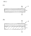
- the electromagnetic wave transmission body 4 of this embodying mode include an Al x Ga 1- x N single crystal having a major surface, and it is not necessary that, as shown in Fig. 2A , the entire electromagnetic wave transmission body be formed of the Al x Ga 1- x N single crystal 2, it being possible as well, as shown in Fig. 2B , that a part of the electromagnetic wave transmission body 4 be formed of the Al x Ga 1-x N single crystal 2. In the case, as shown in Fig.
- the electromagnetic wave transmission body 4 includes an Al x Ga 1- x N single crystal 2 having a 2 m major surface and an electromagnetic-radiation transmissive material 3 other than an Al x Ga 1 -x N single crystal
- the electromagnetic-radiation transmissive material 3 is not particularly limited, as long as it does not hinder the transmission of electromagnetic radiation and can, for example, be quartz glass, alumina, or an AIN sinter or the like.
- the electromagnetic wave transmission body 4 is disposed so that the 2 m major surface of the Al x Ga 1- x N single crystal 2 is placed in a severe environment (for example, exposed to a plasma of a corrosive gas, or a high-power plasma).
- the Al x Ga 1- x N single crystal included in the electromagnetic wave transmission body 4 of this embodiment has a dielectric loss tangent of 5 ⁇ 10 -3 or lower when a 1-MHz RF signal applied thereto at an atmospheric temperature of 25°C, the dielectric losses of the electromagnetic wave transmission body of this embodying mode are extremely low, even when high-frequency electromagnetic radiation is transmitted.
- the oxygen concentration of the Al x Ga 1- x N single crystal 2 included in the electromagnetic wave transmission body 4 of this embodying mode is preferably 1 ⁇ 10 18 cm -3 or lower, more preferably 5 ⁇ 10 17 cm -3 or lower, and yet more preferably 3 ⁇ 10 17 cm -3 or lower.
- the Al x Ga 1- x N single crystal 2 included in the electromagnetic wave transmission body 4 of this embodying mode is not particularly limited in this regard, from the standpoint of reducing the dislocation density and suppressing the formation of the complex defect V Al -O N so as to make the dielectric loss tangent small, the dislocation density is preferably 1 ⁇ 10 6 cm -2 or lower, more preferably 5 ⁇ 10 5 cm -2 or lower, and yet more preferably 1 ⁇ 10 5 cm -2 or lower.
- the electromagnetic wave transmission body 4 of this embodying mode has a span or diameter that is preferably 50 mm or greater and a thickness that is preferably 300 ⁇ m or greater. From the same standpoint, the span or diameter is preferably 50 mm or greater and more preferably 100 mm or greater. Also, the thickness of the electromagnetic wave transmission body is preferably 300 ⁇ m or greater, more preferably 1000 ⁇ m or greater, and yet more preferably 3000 ⁇ m or greater.
- the span of the Al x Ga 1- x N single crystal in the case in which a major surface thereof is polygonal, means the distance between two arbitrarily specified opposing vertices that surround a center part.
- the diameter of the Al x Ga 1- x N single crystal in the case in which the major surface of the single crystal is circular or elliptical, means an arbitrarily specified diameter on the major surface.
- the RMS surface roughness is preferably 100 nm or less, more preferably 10 nm or less, and yet more preferably 1 nm or less.
- a preferable method is a method of forming a desired shape from an Al x Ga 1- x N single crystal grown by a vapor-phase epitaxy (sublimation growth and HVPE being particularly preferable) or a method of adhering another electromagnetic wave transmission body (for example, quartz glass, alumina, or an AIN sinter) to an Al x Ga 1- x N single crystal processed to the desired shape.
- one method is that the Al x Ga 1- x N single crystal grown on the major surface underlying substrate 1 is sliced along a plane that is parallel to the major surface of the underlying substrate 1, and the sliced surface is planarized by grinding and/or polishing so as to form the major surfaces 2 m and 2 n .
- one method is that of adhering another electromagnetic-radiation transmissive material to one of the major surfaces, 2 n , of the planarized Al x Ga 1- x N single crystal 2 having 2 m and 2 n major surfaces.
- an electromagnetic wave transmission body 4 that includes an Al x Ga 1- x N single crystal 2 having a 2 m major surface is obtained.
- AlN single crystal was grown as the Al x Ga 1- x N single crystal 2 by the method of sublimation.
- a vertical sublimation furnace 10 of the RF induction heating type such as shown in Fig. 1 , was used.
- a tungsten carbide crucible 12 having an exhaust port 12c was provided in the reaction vessel 11 in the vertical sublimation furnace 10, and a heating element 14 was provided that surrounded the crucible 12 to provide ventilation from the inside of the crucible to the outside.
- An RF induction heating coil 15 is provided at the center part outside the reaction vessel so as to heat the heating element 14 that heats the crucible 12.
- an N 2 gas intake port 11a and an N 2 exhaust port 11c for the purpose of causing flow of N 2 gas, and a pyrometer 16 for measuring the temperatures of the upper surface and the lower surface of the crucible 12 are provided outside the crucible 12 of the reaction vessel 11, at the end part of the reaction vessel 11.
- AIN powder was placed in the bottom part of the tungsten carbide crucible 12, and an AIN underlying substrate 1 having a diameter of 12 mm and a thickness of 1 mm was disposed at the top part of the crucible as the underlying substrate 1.
- the AlN underlying substrate 1 is formed of AIN single crystal, and had a dislocation density of 1 ⁇ 10 6 cm -2 or lower and a full width at half-maximum of the x-ray diffraction peak for the (0002) surface of 100 arcsec or smaller.
- the AlN underlying substrate 1 was held to the crucible lid 13, which was made of the same material as the crucible 12, so the AIN surface thereof opposes the Al y Ga 1- y N source material 5.
- the RF induction heating coil 15 was used to raise the temperature within the crucible 12.
- the amounts of N 2 gas introduced and exhausted were controlled so that the partial pressure of the N 2 gas was 10 kPa to 100 kPa.
- the temperature of the AIN underlying substrate 1 side of the crucible was made higher than the temperature of the Al y Ga 1- y N source material 5 side, so that the surface of the AIN underlying substrate 1 was cleaned by etching, and impurities released from AIN underlying substrate 1 and the inner part of the crucible 12 were removed via the exhaust port 12c.
- N 2 gas continued to flow to the outside of the crucible 12 in the reaction vessel 11, and control was done so that the N 2 gas partial pressure outside the crucible 12 inside the reaction vessel 11 was 10 kPa to 100 kPa, by controlling the amount of N 2 gas introduced and the amount of N 2 gas exhausted.
- AIN single crystal Al x Ga 1- x N single crystal 2
- the AIN single crystal that was obtained had a diameter of approximately 12 mm and a thickness of approximately 4.2 mm, and was estimated to have been formed at a growth rate of 105 ⁇ m/hour.
- the obtained AIN single crystal (Al x Ga 1- x N single crystal 2) was sliced along a plane parallel to the AIN single crystal growth plane so as to obtain several sheet-shaped AIN single crystals (Al x Ga 1- x N single crystal 2) and sheet-shaped AIN single crystals adjacent to the above-noted AIN single crystals.
- the 2 m and 2 n major surfaces of each side of both AIN single crystals were ground and polished to planarize. The former was evaluated by applying to them an RF signal, and the latter was used in another evaluation.
- the RMS surface roughness of the 2 m major surface of the sheet-shaped AIN single crystals was found to be a small value of 28 nm in a 50- ⁇ m square (square 50 ⁇ m ⁇ 50 ⁇ m) area, as measured by an AFM (atomic force microscope).
- the 2 m major surface is placed in a severe environment (for example, exposed to a plasma of a corrosive gas or a high-power plasma). For this reason, it is preferable that the 2 m major surface been highly resistance to chemical action, for example, making the Al-surface be the outside surface.
- the sheet-shaped AIN single crystal at the uppermost part of the AIN single crystal has a small value of 35 arcsec for the full width at half-maximum of the x-ray diffraction peak for the (0002) plane, and was a crystal of high quality. Additionally, upon determining the dislocation density of the sheet-shaped AIN single crystal using the EPD (etch pit density) method, it was found to be a low value of 3 ⁇ 10 4 cm -2 .
- the dislocation density was determined by the EPD method by etching the sheet-shaped AIN single crystal for 30 minutes at 250°C in a molten KOH : NaOH with a mass ratio of 1 : 1, and then using a microscope to determine the number of etch pits per unit surface area occurring in the major surface of the AIN single crystal.
- an LCR meter 20 was used to measure the dielectric constant and the dielectric loss tangent of the AIN single crystal (Al x Ga 1- x N single crystal 2) with a 1-MHz RF signal applied at an atmospheric temperature of 25°C.
- Ti/Al/Ti/Au electrodes (with thicknesses of 20 nm/100 nm/20 nm/50 nm) were vapor deposited as electrodes 8 onto the 2m and 2n major surfaces on each side of the sheet-shaped AIN (Al x Ga 1- x N single crystal 2), and placed in an infrared lamp heating oven and annealed for 1 minute at 600°C in an N 2 atmosphere to cause alloying of the electrodes 8.
- the dielectric constant and dielectric loss tangent of the sheet-shaped AIN single crystal were measured at an atmospheric temperature of 25°C, with a 1-MHz AC signal applied across the electrodes 8 that were formed on the 2m and 2n major surfaces of the sheet-shaped AIN single crystal.
- the dielectric constant ⁇ and the dielectric loss tangent tan ⁇ were, respectively, 8.9 and 5.3 ⁇ 10 -5 .
- the oxygen concentration in the AIN single crystal upon performing SIMS (secondary ion mass spectrometry) using a sample of 5 mm square cut away from the center of another sheet-shaped AIN single crystal, was a low value of 5.2 ⁇ 10 17 cm -3 .
- an AIN single crystal (Al x Ga 1- x N single crystal 2) was grown in the same way as in Embodiment 1.
- the AIN single crystal that was obtained had a thickness of 5.2 mm, a growth rate of 130 ⁇ m/hour, a full width at half-maximum of the x-ray diffraction peak for the (0002) plane of 42 arcsec, a dislocation density of 4.0 ⁇ 10 4 cm -2 , an RMS surface roughness of 43 nm, a dielectric constant ⁇ of 8.7 and dielectric loss tangent tan ⁇ of 7.2 ⁇ 10 -5 with a 1-MHz RF signal applied at an atmospheric temperature of 25°C, and an oxygen concentration of 4.7 ⁇ 10 17 cm -3 .
- Table I The results are summarized in Table I.
- an AIN single crystal (Al x Ga 1- x N single crystal 2) was grown in the same way as in Embodiment 1.
- the AIN single crystal that was obtained had a thickness of 5.8 mm, a growth rate of 145 ⁇ m/hour, a full width at half-maximum of the x-ray diffraction peak for the (0002) plane of 72 arcsec, a dislocation density of 9.0 ⁇ 10 4 cm -2 , an RMS surface roughness of 28 nm, a dielectric constant ⁇ of 8.7 and dielectric loss tangent tan ⁇ of 2.8 ⁇ 10 -4 with a 1-MHz RF signal applied at an atmospheric temperature of 25°C, and an oxygen concentration of 5.1 ⁇ 10 17 cm -3 .
- Table I The results are summarized in Table I.
- a 50.8-mm (2-inch) diameter SiC underlying substrate was used as the underlying substrate 1 and, with the exception of using N 2 gas at a partial pressure of 50 kPa and making the temperature of the SiC underlying substrate 1 side be 1730°C, and making the temperature of the AIN powder (Al y Ga 1- y N source material 5) side be 2050°C, an AIN single crystal (Al x Ga 1- x N single crystal 2) was grown in the same way as in Embodiment 1.
- the AIN single crystal that was obtained had a thickness of 4.3 mm, a growth rate of 107.5 ⁇ m/hour, a full width at half-maximum of the x-ray diffraction peak for the (0002) plane of 115 arcsec, a dislocation density of 5.6 ⁇ 10 5 cm -2 , an RMS surface roughness of 40 nm, a dielectric constant ⁇ of 8.6 and dielectric loss tangent tan ⁇ of 1.6 ⁇ 10 -3 with a 1-MHz RF signal having been applied to the crystal at an atmospheric temperature of 25°C, and an oxygen concentration of 1.4 ⁇ 10 18 cm -3 .
- the cavity resonator method was used to measure the dielectric constant and the dielectric loss tangent of the AIN single crystal (Al x Ga 1-X N single crystal 2) with a 1-GHz RF signal applied, at an atmospheric temperature of 25°C.
- the measurement system shown in Fig. 4 was used.
- a columnar shaped cavity resonator 31 is formed of a good conductor, such as copper or aluminum, and the inside thereof is hollow. This hollow space is used as a resonance field for electromagnetic radiation.
- the cavity resonator 31 has an input signal aperture 32 for the input of an electromagnetic RF signal to excite the resonator, and a signal detection output aperture 33 for measuring the resonance condition.
- An RF signal caused by electromagnetic radiation generated by an RF signal generator 35 is, for example, input to the cavity resonator 31 from the aperture 32 via a signal line 36.
- an electromagnetic field resonance condition of a prescribed mode is caused inside the cavity resonator 31.
- a signal that indicates the resonance condition is extracted from the aperture 33 via a signal line 37, and sent to a resonance condition analyzer 38, such as a spectrum analyzer.
- the resonance condition analyzer 38 measures the resonance condition from the detected signal and, from the measurement results, makes it possible to determine factors characterizing the dielectric properties of the AIN single crystal that is the object under measurement.
- a 50.8-mm (2-inch) diameter AIN underlying substrate was used as the underlying substrate 1 and, with the exception of using N 2 gas at a partial pressure of 50 kPa and making the temperature of the AIN underlying substrate 1 side be 1930°C, and making the temperature of the AIN powder (Al y Ga 1- y N source material 5) side be 2310°C, an AIN single crystal (Al x Ga 1- x N single crystal 2) was grown in the same way as in Embodiment 1.
- the AIN single crystal that was obtained had a thickness of 3.2 mm, a growth rate of 80 ⁇ m/hour, a full width at half-maximum of the x-ray diffraction peak for the (0002) plane of 86 arcsec, a dislocation density of 1.3 ⁇ 10 5 cm -2 , an RMS surface roughness of 35 nm, a dielectric constant ⁇ of 8.8 and dielectric loss tangent tan ⁇ of 6.2 ⁇ 10 -4 with a 1-MHz RF signal applied at an atmospheric temperature of 25°C, a dielectric constant ⁇ of 8.7 and dielectric loss tangent tan ⁇ of 6.5 ⁇ 10 -4 with a 1-GHz RF signal applied at an atmospheric temperature of 25°C, and an oxygen concentration of 5.8 ⁇ 10 17 cm -3 .
- an Al x Ga 1- x N single crystal is obtained that has a dielectric loss tangent of 5 ⁇ 10 -3 or lower with a 1-MHz RF signal applied at an atmospheric temperature of 25°C and/or a dielectric loss tangent of 5 ⁇ 10 -3 or lower with a 1-GHz RF signal applied at an atmospheric temperature of 25°C.
Landscapes
- Chemical & Material Sciences (AREA)
- Engineering & Computer Science (AREA)
- Crystallography & Structural Chemistry (AREA)
- Materials Engineering (AREA)
- Metallurgy (AREA)
- Organic Chemistry (AREA)
- Chemical Kinetics & Catalysis (AREA)
- General Chemical & Material Sciences (AREA)
- Inorganic Chemistry (AREA)
- Crystals, And After-Treatments Of Crystals (AREA)
Abstract
Description
- The present invention relates to Al x Ga1-xN (0 < x ≤ 1) single crystals and electromagnetic wave transmission bodies containing Al x Ga1-x N single crystals, suitably utilized in electronic components, microelectronic components, optoelectronic components, and like applications.
- In plasma generation apparatuses, which apply radio-frequency power to gases to create plasmas, materials such as quartz glass are employed as an electromagnetic wave transmission body. When exposed to a plasma of non-corrosive gases such as Ar, N2, O2 or SiH4, such electromagnetic wave transmission bodies emit heat owing, in addition to absorption of the high-frequency energy, to ion bombardment and radiant heat from the plasma, therefore making necessary heat-emission prevention and heat-shock resistance in electromagnetic wave transmission bodies. And when quartz glass as an electromagnetic wave transmission body is exposed to plasma from chlorine- or fluorine-containing corrosive gases corrosive gases such as C1F3, NF3, CF4, CHF3, and SiH2Cl2 for example-a difficulty arises in that the material is etched at a high rate and Si and O, etching by-products from the quartz, mix into the plasma.
- Alumina (aluminum oxide) is effective from the standpoint of resistance to corrosive gases. However, because alumina has poor resistance to heat shock and has a low thermal conductivity, there is the problem of the temperature becoming locally high with a high-power plasma, and thermal stress causing breakage.
- With respect to a high-power plasma, an aluminum nitride sintered ceramic having a high thermal conductivity and a low thermal expansion coefficient has a high resistance to corrosive halogen-based gases, and is preferable to alumina (cf., for example, Japanese Unexamined Pat. App. Pub.
H07-142197 H07-142414 - For this reason, there has been a need for a high-quality electromagnetic wave transmission body having a small (dielectric) dielectric loss tangent so as to suppress heat generation, particularly with respect to high-frequency electromagnetic radiation. In order to solve these problems, control of the silicon concentration in the sinter (cf., for example, Japanese Unexamined Pat. App. Pub. No.
2000-335974 2002-172322 2006-08493 -
- Patent Document 1: Japanese Unexamined Pat. App. Pub. No.
H07-142197 - Patent Document 2: Japanese Unexamined Pat. App. Pub. No.
H07-142414 - Patent Document 3: Japanese Unexamined Pat. App. Pub. No.
2000-335974 - Patent Document 4: Japanese Unexamined Pat. App. Pub. No.
2002-172322 - Patent Document 5: Japanese Unexamined Pat. App. Pub. No.
2006-008493 - However, an aluminum nitride sinter has many crystal grain boundaries and often contains a sintering additive. For this reason, because an aluminum nitride sinter has low thermal conductivity compared to an aluminum nitride single crystal and the coefficient of thermal expansion thereof exhibits local variations, there is a limitation to the increase in resistance to heat shock.
- Compared to aluminum nitride single crystals, an aluminum nitride sinter has many crystal defects, and because a sintering aide such as Al2O3, Y2O5, CaO, or MgO is used as a source material, the oxygen concentration is high. For this reason, an aluminum nitride sinter has a high dielectric loss tangent, and there is the problem that when high-power RF electrical power is applied, the temperature increases sharply and the dielectric properties change.
- Additionally, it is difficult to achieve planarity of the surface because loosening of crystal grains occurs when the surface of an aluminum nitride sinter is polished.
- Accordingly, an object of the present invention is to solve the above-noted problems and to make available an Al x Ga1-x N single crystal suitable as an electromagnetic wave transmission body and an electromagnetic wave transmission body that includes the Al x Ga1-x N single crystal.
- The present invention is an Al x Ga1-x N (0 < x ≤ 1) single crystal having a dielectric loss tangent of 5 × 10⁻³ or lower when an RF signal of at least either 1 MHz or 1 GHz is applied to the crystal at an atmospheric temperature of 25°C.
- The Al x Ga1-x N single crystal of the present invention can be made to have a dielectric loss tangent of 5 × 10⁻³ or lower with a 1-MHz RF signal applied thereto and also made to have a dielectric loss tangent of 5 × 10⁻³ or lower with a 1-GHz RF signal applied thereto. Also, the oxygen concentration of the Al x Ga1-x N single crystal of the present invention can be made 1 × 1018 cm-3 or lower. And the dislocation density of the Al x Ga1-x N single crystal of the present invention can be made 1 × 106 cm-2 or lower. The span or diameter of the Al x Ga1-x N single crystal of the present invention can be made 10 mm or greater and the thickness thereof can be made 300 µm or lower. The RMS surface roughness of the Al x Ga1-x N single crystal can be made 100 nm or lower.
- Also, the present invention is an electromagnetic wave transmission body that includes an Al x Ga1-x N (0 < x ≤ 1) single crystal having a major plane, wherein the dielectric loss tangent of the Al x Ga1-x N single crystal is 5 × 10⁻³ or lower with at least either a 1-MHz RF signal or a 1-GHz RF signal having been applied thereto at an atmospheric temperature of 25°C.
- In the electromagnetic wave transmission body of the present invention, the Al x Ga1-x N single crystal can be made to have a dielectric loss tangent of 5 × 10⁻³ or lower with a 1-MHz RF signal having been applied thereto and also to have a dielectric loss tangent of 5 × 10⁻³ or lower with a 1-GHz RF signal having been applied thereto. Also, the oxygen concentration of the Al x Ga1-x N single crystal of the present invention can be made 1 × 1018 cm-3 or lower. And the dislocation density of the Al x Ga1-x N single crystal of the present invention can be made 1 × 106 cm-2 or lower. The span or diameter of the Al x Ga1-x N single crystal of the present invention can be made 10 mm or greater, and the thickness thereof can be made 300 µm or greater. The RMS surface roughness of the Al x Ga1-x N single crystal can be made 100 nm or lower.
- The present invention make available an Al x Ga1-x N single crystal preferable as an electromagnetic wave transmission body, as well as an electromagnetic wave transmission body that includes the Al x Ga1-x N single crystal.
-
-
Fig. 1 is a simplified cross-sectional view showing an example of an apparatus and a method for manufacturing an Al x Ga1-x N single crystal of the present invention. -
Fig. 2 is two simplified cross-sectional views showing examples of an electromagnetic wave transmission body of the present invention, wherein (A) shows an example in which the entire electromagnetic wave transmission body is a Al x Ga1-x N single crystal, and (B) shows an example in which a part of the electromagnetic wave transmission body is a Al x Ga1-x N single crystal. -
Fig. 3 is a simplified cross-sectional view showing an example of a method of measuring the dielectric constant and the dielectric loss tangent of an electromagnetic wave transmission body of the present invention. -
Fig. 4 is a simplified cross-sectional view showing another example a method of measuring the dielectric constant and the dielectric loss tangent of an electromagnetic wave transmission body of the present invention. - Compared to an AIN (aluminum nitride) sinter, the Al x Ga1-x N single crystal that is the first embodying mode of the present invention has a high thermal conductivity, and little local variation in the coefficient of thermal expansion. For this reason, even if exposed to a high-frequency plasma, the Al x Ga1-x N single crystal tends to be immune to thermal stress and has a high resistance to heat shock. Also, because the Al x Ga1-x N single crystal of this embodying mode has a dielectric loss tangent of 5 × 10⁻³ or lower when at least either a 1-MHz RF signal or a 1-GHz RF signal is applied thereto at an atmospheric temperature of 25°C, even if high-frequency electromagnetic radiation is transmitted, the dielectric losses are extremely small, making it suitable as an electromagnetic wave transmission body.
- It is preferable that, at an atmospheric temperature of 25°C, the Al x Ga1-x N single crystal of this embodying mode have a dielectric loss tangent of 5 × 10⁻³ or lower when a 1-MHz RF signal is applied thereto and also a dielectric loss tangent of 5 × 10⁻³ or lower when a 1-GHz RF signal is applied thereto. The Al x Ga1-x N single crystal has an extremely low dielectric loss even when transmitting electromagnetic radiation over a broad range of high frequencies spanning from the order of MHz to the order of GHz, and is preferably used as an electromagnetic wave transmission body.
- According to the knowledge of the inventors, oxygen atoms included in an Al x Ga1-x N single crystal are replaced by nitrogen atoms (replacement oxygen atom ON), and also bond to lattice defects (vacancy VAl) in the aluminum, so as to form a complex defect VAl-ON). It is thought that the dielectric loss tangent becomes large by this complex defect VAl-ON forming a dipole.
- From the standpoint of making the oxygen concentration small and suppressing the formation of the complex defect VAl-ON to make the dielectric loss tangent small, therefore, the Al x Ga1-x N single crystal of this embodying mode, although it is not particularly limited in this regard, has an oxygen concentration that is preferably 1 × 1018 cm-3 or lower, and more preferably 3 × 1017 cm-3 or lower.
- From the standpoint of keeping complex defects VAl-ON from forming, the Al x Ga1-x N single crystal of this embodying mode, although not particularly limited in this regard, has a dislocation density that is preferably 1 × 106 cm-2 or lower and more preferably 5 × 105 cm-2 or lower, and yet more preferably 1 × 105 cm-2 or lower.
- Also, from the standpoint of having a size and mechanical strength that are preferable for an electromagnetic wave transmission body, the Al x Ga1-x N single crystal of this embodying mode, although not particularly limited in this regard, has a span or diameter that is preferably 10 mm or greater and a thickness that is preferably 300 µm or greater. From the same standpoint, the span or diameter of the Al x Ga1-x N single crystal is preferably 50 mm or greater and more preferably 100 mm or greater. Also, the thickness of the Al x Ga1-x N single crystal is preferably 300 µm or greater, more preferably 1000 µm or greater, and yet more preferably 3000 µm or greater. In this case, the span of the Al x Ga1-x N single crystal, in the case in which a major surface thereof is polygonal, means the distance between two arbitrarily specified opposing vertices that surround a center part. Also, the diameter of the Al x Ga1-x N single crystal, in the case in which the major surface of the single crystal is circular or elliptical, means an arbitrarily specified diameter on the major surface.
- Although the Al x Ga1-x N single crystal of this embodying mode is not limited in this regard, from the standpoint of increasing the planarity of the surface and making the mutual interaction between the Al x Ga1-x N single crystal and the plasma gas small, the RMS surface roughness is preferably 100 nm or lower, more preferably 10 nm or lower, and yet more preferably 1 nm or lower. The RMS surface roughness as the term is used herein is the root mean square roughness as set forth in JIS B 0601, which means the square root of the average value of the distance (variation) from an average surface to the measured surface.
- From the standpoint of facilitating the manufacture of an Al x Ga1-x N single crystal having both a low oxygen concentration and a low dislocation density, and that has a dielectric loss tangent of 5 × 10⁻³ or lower when at least either a 1-MHz RF signal or a 1-GHz RF signal is applied thereto at an atmospheric temperature of 25°C, although the method of manufacturing an Al x Ga1-x N single crystal of this embodying mode is not particularly limited in this regard, a preferable method is vapor-phase epitaxy, and sublimation growth (cf.
Fig. 1 ) and HVPE (hydride vapor phase epitaxy) are particularly preferable. - From the standpoints noted above, the method of manufacturing the Al x Ga1-x N single crystal of this embodying mode preferably includes a step of preparing an
underlying substrate 1, and a step of growing an Al x Ga1-x Nsingle crystal 2 on theunderlying substrate 1. In this case, theunderlying substrate 1, from the standpoint of making the lattice mismatch between the Al x Ga1-x N single crystal and the underlying substrate small, an AlzGa1-zN single crystal (0 < z < 1) is preferable and an Al z Ga1-z N single crystal in which z = x is more preferable. Also, from the standpoint of facilitating the growth of an Al z Ga1-z N single crystal having a low dislocation density and high crystallization, it is preferable that the Al z Ga1-z N single crystal, which is theunderlying substrate 1, have a dislocation density of 1 ×106 cm-2 or lower, and more preferable that the full width at half-maximum of the x-ray diffraction peak for the (0002) plane be 100 arcsec or lower. - Referring to
Fig. 2 , the electromagneticwave transmission body 4 of another embodying mode of the present invention includes an Al x Ga1-x N single crystal (0 < x ≤ 1) 2 having a 2m major surface, the Al x Ga1-x Nsingle crystal 2 having a dielectric loss tangent of 5 × 10⁻³ or lower when at least either a 1-MHz or a 1-GHz RF signal is applied thereto at an atmospheric temperature of 25°C. For this reason, the electromagnetic wave transmission body of this embodying mode has an extremely small dielectric loss tangent, even when transmitting high-frequency electromagnetic radiation. - Also, the Al x Ga1-x N
single crystal 2 that is included in the electromagneticwave transmission body 4 of this embodying mode preferably has a dielectric loss tangent of 5 × 10⁻³ or lower when a 1-MHz RF signal is applied and also preferably has a dielectric loss tangent of 5 × 10⁻³ or lower when a 1-GHz RF signal is applied. The electromagnetic wave transmission body has an extremely small dielectric loss tangent even when transmitting electromagnetic radiation over a broad range of high frequencies spanning from on the order of MHz to on the order of GHz. - The electromagnetic
wave transmission body 4 of this embodying mode includes an Al x Ga1-x N (0 < x ≤ 1)single crystal 2 having a 2m major surface. The Al x Ga1-x Nsingle crystal 2, compared to an AIN sinter, has smaller local variation in the coefficient of thermal expansion. For this reason, even if the electromagnetic wave transmission body is exposed to a high-frequency plasma at the above-noted 2m main surface of the Al x Ga1-x N single crystal included therein, it tends not to be thermally stressed, and has a high resistance to heat shock. - It is sufficient that the electromagnetic
wave transmission body 4 of this embodying mode include an Al x Ga1-x N single crystal having a major surface, and it is not necessary that, as shown inFig. 2A , the entire electromagnetic wave transmission body be formed of the Al x Ga1-x Nsingle crystal 2, it being possible as well, as shown inFig. 2B , that a part of the electromagneticwave transmission body 4 be formed of the AlxGa1-xNsingle crystal 2. In the case, as shown inFig. 2B , in which the electromagneticwave transmission body 4 includes an Al x Ga1-x Nsingle crystal 2 having a 2m major surface and an electromagnetic-radiation transmissive material 3 other than an Al x Ga1-x N single crystal, the electromagnetic-radiation transmissive material 3 is not particularly limited, as long as it does not hinder the transmission of electromagnetic radiation and can, for example, be quartz glass, alumina, or an AIN sinter or the like. In this case, the electromagneticwave transmission body 4 is disposed so that the 2m major surface of the Al x Ga1-x Nsingle crystal 2 is placed in a severe environment (for example, exposed to a plasma of a corrosive gas, or a high-power plasma). - Because the Al x Ga1-x N single crystal included in the electromagnetic
wave transmission body 4 of this embodiment has a dielectric loss tangent of 5 × 10⁻³ or lower when a 1-MHz RF signal applied thereto at an atmospheric temperature of 25°C, the dielectric losses of the electromagnetic wave transmission body of this embodying mode are extremely low, even when high-frequency electromagnetic radiation is transmitted. - From the standpoint of making the oxygen concentration of the Al x Ga1-x N
single crystal 2 included in the electromagneticwave transmission body 4 of this embodying mode be small and suppressing the formation of the complex defect VAl-ON so as to make the dielectric loss tangent small, the oxygen concentration is preferably 1 × 1018 cm-3 or lower, more preferably 5 × 1017 cm-3 or lower, and yet more preferably 3 × 1017 cm-3 or lower. - Although the Al x Ga1-x N
single crystal 2 included in the electromagneticwave transmission body 4 of this embodying mode is not particularly limited in this regard, from the standpoint of reducing the dislocation density and suppressing the formation of the complex defect VAl-ON so as to make the dielectric loss tangent small, the dislocation density is preferably 1 × 106 cm-2 or lower, more preferably 5 × 105 cm-2 or lower, and yet more preferably 1 × 105 cm-2 or lower. - Also, from the standpoint of having a size that is preferable for use as an electromagnetic wave transmission body and mechanical strength, the electromagnetic
wave transmission body 4 of this embodying mode, although not particularly limited in this regard, has a span or diameter that is preferably 50 mm or greater and a thickness that is preferably 300 µm or greater. From the same standpoint, the span or diameter is preferably 50 mm or greater and more preferably 100 mm or greater. Also, the thickness of the electromagnetic wave transmission body is preferably 300 µm or greater, more preferably 1000 µm or greater, and yet more preferably 3000 µm or greater. In this case, the span of the Al x Ga1-x N single crystal, in the case in which a major surface thereof is polygonal, means the distance between two arbitrarily specified opposing vertices that surround a center part. Also, the diameter of the Al x Ga1-x N single crystal, in the case in which the major surface of the single crystal is circular or elliptical, means an arbitrarily specified diameter on the major surface. - From the standpoint of making the interaction between the Al x Ga1-x N single crystal and the plasma gas small, although the electromagnetic wave transmission body of this embodying mode is not particularly limited in this regard, the RMS surface roughness is preferably 100 nm or less, more preferably 10 nm or less, and yet more preferably 1 nm or less.
- From the standpoint of facilitating the manufacture of an Al x Ga1-x N single crystal having both a low oxygen concentration and a low dislocation density, and that has a dielectric loss tangent of 5 × 10⁻³ or lower when at least either a 1-MHz RF signal or a 1-GHz RF signal is applied thereto at an atmospheric temperature of 25°C, although the method of manufacturing the electromagnetic wave transmission body of this embodying mode is not particularly limited in this regard, a preferable method is a method of forming a desired shape from an Al x Ga1-x N single crystal grown by a vapor-phase epitaxy (sublimation growth and HVPE being particularly preferable) or a method of adhering another electromagnetic wave transmission body (for example, quartz glass, alumina, or an AIN sinter) to an Al x Ga1-x N single crystal processed to the desired shape.
- As a method for forming a desired shape from an Al x Ga1-x N single crystal grown by vapor-phase epitaxy (and particularly by sublimation or HVPE), although there is no particular limitation in this regard, referring to
Fig. 1 andFig. 2A , one method is that the Al x Ga1-x N single crystal grown on the majorsurface underlying substrate 1 is sliced along a plane that is parallel to the major surface of theunderlying substrate 1, and the sliced surface is planarized by grinding and/or polishing so as to form themajor surfaces Fig. 2B , is that of adhering another electromagnetic-radiation transmissive material to one of the major surfaces, 2n, of the planarized Al x Ga1-x Nsingle crystal 2 having 2m and 2n major surfaces. In this manner, an electromagneticwave transmission body 4 that includes an Al x Ga1-x Nsingle crystal 2 having a 2m major surface is obtained. - An AlN single crystal was grown as the Al x Ga1-x N
single crystal 2 by the method of sublimation. In the growth of the AlN single crystal (Al x Ga1-x N single crystal 2) in this embodiment example, avertical sublimation furnace 10 of the RF induction heating type, such as shown inFig. 1 , was used. Atungsten carbide crucible 12 having anexhaust port 12c was provided in thereaction vessel 11 in thevertical sublimation furnace 10, and aheating element 14 was provided that surrounded thecrucible 12 to provide ventilation from the inside of the crucible to the outside. An RFinduction heating coil 15 is provided at the center part outside the reaction vessel so as to heat theheating element 14 that heats thecrucible 12. Additionally, an N2gas intake port 11a and an N2 exhaust port 11c for the purpose of causing flow of N2 gas, and apyrometer 16 for measuring the temperatures of the upper surface and the lower surface of thecrucible 12 are provided outside thecrucible 12 of thereaction vessel 11, at the end part of thereaction vessel 11. - Referring to
Fig. 1 , as the Al y Ga1-y N (0 < y ≤1)source material 5, AIN powder was placed in the bottom part of thetungsten carbide crucible 12, and an AINunderlying substrate 1 having a diameter of 12 mm and a thickness of 1 mm was disposed at the top part of the crucible as theunderlying substrate 1. The AlNunderlying substrate 1 is formed of AIN single crystal, and had a dislocation density of 1 × 106 cm-2 or lower and a full width at half-maximum of the x-ray diffraction peak for the (0002) surface of 100 arcsec or smaller. The AlNunderlying substrate 1 was held to thecrucible lid 13, which was made of the same material as thecrucible 12, so the AIN surface thereof opposes the Al y Ga1-yN source material 5. - Next, as N2 gas was caused to flow into the
reaction vessel 11, the RFinduction heating coil 15 was used to raise the temperature within thecrucible 12. The amounts of N2 gas introduced and exhausted were controlled so that the partial pressure of the N2 gas was 10 kPa to 100 kPa. During the temperature rise within thecrucible 12, the temperature of the AINunderlying substrate 1 side of the crucible was made higher than the temperature of the Al y Ga1-yN source material 5 side, so that the surface of the AINunderlying substrate 1 was cleaned by etching, and impurities released from AINunderlying substrate 1 and the inner part of thecrucible 12 were removed via theexhaust port 12c. - Next, after the temperature of the AIN powder (Al y Ga1-y N source material 5) side of the
crucible 12 reached 2050°C, control was performed so that the N2 partial pressure was 80 kPa, the temperature on the AIN powder (Al y Ga1-y N source material 5) side was 2350°C, and the temperature on the AlNunderlying substrate 1 side was 1910°C, and the AIN was sublimated from the AIN power (Al y Ga1-y N source material 5), the AIN single crystal being re-solidified on top of the AINunderlying substrate 1 that had been placed at the upper part of thecrucible 12 so as to grow the AIN single crystal (Al x Ga1-x N single crystal 2). Even during the growth of the AIN single crystal, N2 gas continued to flow to the outside of thecrucible 12 in thereaction vessel 11, and control was done so that the N2 gas partial pressure outside thecrucible 12 inside thereaction vessel 11 was 10 kPa to 100 kPa, by controlling the amount of N2 gas introduced and the amount of N2 gas exhausted. After growing an AIN single crystal (Al x Ga1-x N single crystal 2) on the AINunderlying substrate 1 for 40 hours under the above-noted conditions, cooling to room temperature (25°C) was done and an AIN single crystal was obtained. The AIN single crystal that was obtained had a diameter of approximately 12 mm and a thickness of approximately 4.2 mm, and was estimated to have been formed at a growth rate of 105 µm/hour. - Referring to
Fig. 1 andFig. 2A , the obtained AIN single crystal (Al x Ga1-x N single crystal 2) was sliced along a plane parallel to the AIN single crystal growth plane so as to obtain several sheet-shaped AIN single crystals (Al x Ga1-x N single crystal 2) and sheet-shaped AIN single crystals adjacent to the above-noted AIN single crystals. The 2m and 2n major surfaces of each side of both AIN single crystals were ground and polished to planarize. The former was evaluated by applying to them an RF signal, and the latter was used in another evaluation. The RMS surface roughness of the 2m major surface of the sheet-shaped AIN single crystals was found to be a small value of 28 nm in a 50-µm square (square 50 µm × 50 µm) area, as measured by an AFM (atomic force microscope). In an embodying mode as an electromagnetic wave transmission body, the 2m major surface is placed in a severe environment (for example, exposed to a plasma of a corrosive gas or a high-power plasma). For this reason, it is preferable that the 2m major surface been highly resistance to chemical action, for example, making the Al-surface be the outside surface. - The sheet-shaped AIN single crystal at the uppermost part of the AIN single crystal has a small value of 35 arcsec for the full width at half-maximum of the x-ray diffraction peak for the (0002) plane, and was a crystal of high quality. Additionally, upon determining the dislocation density of the sheet-shaped AIN single crystal using the EPD (etch pit density) method, it was found to be a low value of 3 × 104 cm-2. The dislocation density was determined by the EPD method by etching the sheet-shaped AIN single crystal for 30 minutes at 250°C in a molten KOH : NaOH with a mass ratio of 1 : 1, and then using a microscope to determine the number of etch pits per unit surface area occurring in the major surface of the AIN single crystal.
- Referring to
Fig. 3 , anLCR meter 20 was used to measure the dielectric constant and the dielectric loss tangent of the AIN single crystal (Al x Ga1-x N single crystal 2) with a 1-MHz RF signal applied at an atmospheric temperature of 25°C. Specifically, Ti/Al/Ti/Au electrodes (with thicknesses of 20 nm/100 nm/20 nm/50 nm) were vapor deposited aselectrodes 8 onto the 2m and 2n major surfaces on each side of the sheet-shaped AIN (Al x Ga1-x N single crystal 2), and placed in an infrared lamp heating oven and annealed for 1 minute at 600°C in an N2 atmosphere to cause alloying of theelectrodes 8. Next, using theLCR meter 20, the dielectric constant and dielectric loss tangent of the sheet-shaped AIN single crystal were measured at an atmospheric temperature of 25°C, with a 1-MHz AC signal applied across theelectrodes 8 that were formed on the 2m and 2n major surfaces of the sheet-shaped AIN single crystal. The dielectric constant ε and the dielectric loss tangent tan δ were, respectively, 8.9 and 5.3 × 10⁻⁵. - Also, the oxygen concentration in the AIN single crystal, upon performing SIMS (secondary ion mass spectrometry) using a sample of 5 mm square cut away from the center of another sheet-shaped AIN single crystal, was a low value of 5.2 × 1017 cm-3.
- With the exception of using N2 gas at a partial pressure of 50 kPa and making the temperature of the AIN powder (Al y Ga1-y N source material 5) side be 2300°C, an AIN single crystal (Al x Ga1-x N single crystal 2) was grown in the same way as in
Embodiment 1.
The AIN single crystal that was obtained had a thickness of 5.2 mm, a growth rate of 130 µm/hour, a full width at half-maximum of the x-ray diffraction peak for the (0002) plane of 42 arcsec, a dislocation density of 4.0 × 104 cm-2 , an RMS surface roughness of 43 nm, a dielectric constant ε of 8.7 and dielectric loss tangent tan δ of 7.2 × 10⁻⁵ with a 1-MHz RF signal applied at an atmospheric temperature of 25°C, and an oxygen concentration of 4.7 × 1017 cm-3. The results are summarized in Table I. - With the exception of using N2 gas at a partial pressure of 10 kPa and making the temperature of the AIN powder (Al y Ga1-y N source material 5) side be 2250°C, an AIN single crystal (Al x Ga1-x N single crystal 2) was grown in the same way as in
Embodiment 1. The AIN single crystal that was obtained had a thickness of 5.8 mm, a growth rate of 145 µm/hour, a full width at half-maximum of the x-ray diffraction peak for the (0002) plane of 72 arcsec, a dislocation density of 9.0 × 104 cm-2, an RMS surface roughness of 28 nm, a dielectric constant ε of 8.7 and dielectric loss tangent tan δ of 2.8 × 10⁻⁴with a 1-MHz RF signal applied at an atmospheric temperature of 25°C, and an oxygen concentration of 5.1 × 1017 cm-3. The results are summarized in Table I. - A 50.8-mm (2-inch) diameter SiC underlying substrate was used as the
underlying substrate 1 and, with the exception of using N2 gas at a partial pressure of 50 kPa and making the temperature of the SiCunderlying substrate 1 side be 1730°C, and making the temperature of the AIN powder (Al y Ga1-y N source material 5) side be 2050°C, an AIN single crystal (Al x Ga1-x N single crystal 2) was grown in the same way as inEmbodiment 1.
The AIN single crystal that was obtained had a thickness of 4.3 mm, a growth rate of 107.5 µm/hour, a full width at half-maximum of the x-ray diffraction peak for the (0002) plane of 115 arcsec, a dislocation density of 5.6 × 105 cm-2 , an RMS surface roughness of 40 nm, a dielectric constant ε of 8.6 and dielectric loss tangent tan δ of 1.6 × 10⁻³ with a 1-MHz RF signal having been applied to the crystal at an atmospheric temperature of 25°C, and an oxygen concentration of 1.4 × 1018 cm-3. - Referring to
Fig. 4 , the cavity resonator method was used to measure the dielectric constant and the dielectric loss tangent of the AIN single crystal (AlxGa1-XN single crystal 2) with a 1-GHz RF signal applied, at an atmospheric temperature of 25°C. In the cavity resonator method, the measurement system shown inFig. 4 was used. Specifically, a columnar shapedcavity resonator 31 is formed of a good conductor, such as copper or aluminum, and the inside thereof is hollow. This hollow space is used as a resonance field for electromagnetic radiation. Thecavity resonator 31 has aninput signal aperture 32 for the input of an electromagnetic RF signal to excite the resonator, and a signaldetection output aperture 33 for measuring the resonance condition. An RF signal caused by electromagnetic radiation generated by anRF signal generator 35 is, for example, input to thecavity resonator 31 from theaperture 32 via asignal line 36. By doing this, an electromagnetic field resonance condition of a prescribed mode is caused inside thecavity resonator 31. A signal that indicates the resonance condition is extracted from theaperture 33 via asignal line 37, and sent to a resonance condition analyzer 38, such as a spectrum analyzer. The resonance condition analyzer 38 measures the resonance condition from the detected signal and, from the measurement results, makes it possible to determine factors characterizing the dielectric properties of the AIN single crystal that is the object under measurement. - Specifically, in the above-noted measurement system, detection is made of the change in the resonance condition between the condition in which a 1 mm × 1 mm × 30 mm AIN crystal (Al x Ga1-x N single crystal 2) sample cut from another sheet-shaped AIN single crystal is placed in the cavity resonator and the condition in which it is removed therefrom, and a calculation is performed on the change in resonance condition, so as to determine the dielectric constant ε and the dielectric loss tangent tan δ of the AIN single crystal. The dielectric constant ε and the dielectric loss tangent tan δ obtained in this manner for AIN single crystal to which a 1-GHz RF signal was applied at an atmospheric temperature of 25°C were, respectively, 8.5 and 1.9 × 10⁻³. The results are summarized in Table I.
- A 50.8-mm (2-inch) diameter AIN underlying substrate was used as the
underlying substrate 1 and, with the exception of using N2 gas at a partial pressure of 50 kPa and making the temperature of the AINunderlying substrate 1 side be 1930°C, and making the temperature of the AIN powder (Al y Ga1-y N source material 5) side be 2310°C, an AIN single crystal (Al x Ga1-x N single crystal 2) was grown in the same way as inEmbodiment 1. The AIN single crystal that was obtained had a thickness of 3.2 mm, a growth rate of 80 µm/hour, a full width at half-maximum of the x-ray diffraction peak for the (0002) plane of 86 arcsec, a dislocation density of 1.3 × 105 cm-2 , an RMS surface roughness of 35 nm, a dielectric constant ε of 8.8 and dielectric loss tangent tan δ of 6.2 × 10⁻⁴ with a 1-MHz RF signal applied at an atmospheric temperature of 25°C, a dielectric constant ε of 8.7 and dielectric loss tangent tan δ of 6.5 × 10⁻⁴ with a 1-GHz RF signal applied at an atmospheric temperature of 25°C, and an oxygen concentration of 5.8 × 1017 cm-3 . The results are summarized in Table I.Table I. Embodiment 1 Embodiment 2Embodiment 3Embodiment 4Embodiment 5Al x Ga1-x N Crystal growth conditions Underlying substrate Chemical composition AIN AIN AIN SiC AlN Diameter (mm) 12 12 12 50.8 50.8 Al y Ga1-y N source material AIN AIN AIN AIN AIN N2 gas partial pressure (kPa) 80 50 10 50 50 Underlying substrate side temperature (°C) 1910 1910 1910 1730 1930 Al y Ga1-y N source material side temperature (°C) 2350 2300 2250 2050 2310 Al x Ga1-x N crystal AIN AIN AIN AIN AIN Crystal growth time (hr) 40 40 40 40 40 Al x Ga1-x N Crystal characteristics Crystal growth thickness (mm) 4.2 5.2 5.8 4.3 3.2 Crystal growth rate (µm/hr) 105 130 145 107.5 80 x-ray diffraction peak full width at half-max. (arcsec) 35 42 72 115 86 Dislocation density (cm-2) 3.0× 10⁴ 4.0× 10⁴ 9.0×10⁴ 5.6×10⁵ 1.3×10⁵ RMS surface roughness (nm) 28 43 28 40 35 1 MHz Dielectric constant ε 8.9 8.7 8.7 8.6 8.8 Dielectric loss tangent tan δ 5.3×10⁻⁵ 7.2×10⁻⁵ 2.8×10⁻⁴ 1.6×10⁻³ 6.2×10⁻⁴ 1 GHz Dielectric constant ε - - - 8.5 8.7 Dielectric loss tangent tan δ - - - 1.9×10⁻³ 6.5 ×10⁻⁴ Oxygen concentration (cm-3) 5.2×10¹⁷ 4.7×10¹⁷ 5.1×10¹⁷ 1.4×10¹⁸ 5.8×10¹⁷ - As is clear from Table I, by reducing the oxygen concentration and the dislocation density (preferably to an oxygen concentration of 1 × 1018 cm-3 or lower and a dislocation density of 1 × 106 cm-2 or lower), an Al x Ga1-x N single crystal is obtained that has a dielectric loss tangent of 5 × 10⁻³ or lower with a 1-MHz RF signal applied at an atmospheric temperature of 25°C and/or a dielectric loss tangent of 5 × 10⁻³ or lower with a 1-GHz RF signal applied at an atmospheric temperature of 25°C.
- The presently disclosed embodying modes and embodiment examples should in all respects be considered to be illustrative and not limiting. The scope of the present invention is set forth not by the foregoing description but by the scope of the claims, and is intended to include meanings equivalent to the scope of the claims and all modifications within the scope.
-
- 1:
- underlying substrate
- 2:
- AlxGa1-x N single crystal
- 2m, 2n:
- major surfaces
- 3:
- other electromagnetic-radiation transmissive material
- 4:
- electromagnetic wave transmission body
- 5:
- AlyGa1-y N source material
- 8:
- electrode
- 10:
- sublimation furnace
- 11:
- reaction vessel
- 11 a:
- N2 gas intake port
- 11 c:
- N2 gas exhaust port
- 12:
- crucible
- 12c:
- exhaust port
- 13:
- crucible lid
- 14:
- heating element
- 15:
- RF induction heating coil
- 16:
- pyrometer
- 20:
- LCR meter
- 31:
- cavity resonator
- 32, 33:
- apertures
- 35:
- RF signal generator
- 36, 37:
- signal lines
- 38:
- resonance condition analyzer
Claims (12)
- An Al x Ga1-x N (0 < x ≤1) single crystal having a dielectric loss tangent of 5 × 10⁻³ or lower with a radio-frequency signal of at least either 1 MHz or 1 GHz having been applied thereto at an atmospheric temperature of 25°C.
- An Al x Ga1-x N single crystal as set forth in claim 1, wherein the dielectric loss tangent is 5 × 10⁻³ or lower with a 1-MHz radio-frequency signal having been applied thereto, and also the dielectric loss tangent is 5 × 10⁻³ or lower with a 1-GHz radio-frequency signal having been applied thereto.
- An Al x Ga1-x N single crystal as set forth in either claim 1 or claim 2, wherein the oxygen concentration is 1 × 1018 cm-3 or lower.
- An Al x Ga1-x N single crystal as set forth in either claim 1 or claim 2, wherein the dislocation density is 1 × 106 cm-2 or lower.
- An Al x Ga1-x N single crystal as set forth in any one of claim 1 to claim 4, wherein:the span or the diameter is 10 mm or greater; andthe thickness is 300 µm or greater.
- An Al x Ga1-x N single crystal as set forth in any one of claim 1 to claim 5, wherein the RMS surface roughness is 100 nm or less.
- An electromagnetic wave transmission body including an Al x Ga1-x N (0 < x ≤1) single crystal having a major surface, wherein the Al x Ga1-x N single crystal has a dielectric loss tangent of 5 × 10⁻³ or lower with a radio-frequency signal of at least either 1 MHz or 1 GHz having been applied thereto at an atmospheric temperature of 25°C.
- An electromagnetic wave transmission body as set forth in claim 7, wherein the Al x Ga1-x N single crystal has a dielectric loss tangent of 5 × 10⁻³ or lower with a 1-MHz radio-frequency signal having been applied thereto, and also has a dielectric loss tangent of 5 × 10⁻³ or lower with a 1-GHz radio-frequency signal having been applied thereto.
- An electromagnetic wave transmission body as set forth in either claim 7 or claim 8, wherein the oxygen concentration of the Al x Ga1-x N single crystal is 1 × 1018 cm-3 or lower.
- An electromagnetic wave transmission body as set forth in either claim 7 or claim 8, wherein the Al x Ga1-x N single crystal has a dislocation density of 1 × 106 cm-2 or lower.
- An electromagnetic wave transmission body as set forth in any one of claim 7 to claim 10, wherein:the span or the diameter is 10 mm or greater; andthe thickness is 300 µm or greater.
- An electromagnetic wave transmission body as set forth in any one of claim 7 to claim 11, wherein the RMS surface roughness is 100 nm or less.
Applications Claiming Priority (3)
| Application Number | Priority Date | Filing Date | Title |
|---|---|---|---|
| JP2008139860 | 2008-05-28 | ||
| JP2009028839A JP2010006685A (en) | 2008-05-28 | 2009-02-10 | AlxGa1-xN SINGLE CRYSTAL AND ELECTROMAGNETIC WAVE TRANSMISSION BODY |
| PCT/JP2009/059501 WO2009145129A1 (en) | 2008-05-28 | 2009-05-25 | AlXGa1-XN SINGLE CRYSTAL AND ELECTROMAGNETIC WAVE TRANSMISSION BODY |
Publications (2)
| Publication Number | Publication Date |
|---|---|
| EP2287370A1 true EP2287370A1 (en) | 2011-02-23 |
| EP2287370A4 EP2287370A4 (en) | 2012-11-28 |
Family
ID=41377004
Family Applications (1)
| Application Number | Title | Priority Date | Filing Date |
|---|---|---|---|
| EP09754637A Withdrawn EP2287370A4 (en) | 2008-05-28 | 2009-05-25 | MONOCRYSTAL OF AL <SB> X </ SB> GA <SB> 1-X </ SB> N AND BODY FOR TRANSMITTING ELECTROMAGNETIC WAVES |
Country Status (5)
| Country | Link |
|---|---|
| US (1) | US20110076453A1 (en) |
| EP (1) | EP2287370A4 (en) |
| JP (1) | JP2010006685A (en) |
| CN (1) | CN102046858A (en) |
| WO (1) | WO2009145129A1 (en) |
Families Citing this family (3)
| Publication number | Priority date | Publication date | Assignee | Title |
|---|---|---|---|---|
| JP2013071855A (en) * | 2011-09-27 | 2013-04-22 | Fujikura Ltd | Method for fixing aluminum nitride seed crystal, pedestal-seed crystal fixed body, method for producing aluminum nitride single crystal, and aluminum nitride single crystal |
| JP6279498B2 (en) * | 2015-02-03 | 2018-02-14 | Sppテクノロジーズ株式会社 | Plasma processing apparatus and plasma processing method |
| CN105483833A (en) * | 2015-11-24 | 2016-04-13 | 北京华进创威电子有限公司 | Dislocation etching method for aluminum nitride single crystal |
Family Cites Families (13)
| Publication number | Priority date | Publication date | Assignee | Title |
|---|---|---|---|---|
| JP3029488B2 (en) * | 1991-05-16 | 2000-04-04 | 東芝セラミックス株式会社 | Plasma discharge member |
| JP2862779B2 (en) | 1993-11-18 | 1999-03-03 | 日本碍子株式会社 | Electromagnetic wave transmitting body |
| JPH07142414A (en) | 1993-09-27 | 1995-06-02 | Fuji Electric Co Ltd | Plasma processing device |
| JP3739028B2 (en) | 1999-05-31 | 2006-01-25 | 東芝セラミックス株式会社 | High frequency transmission body and method for manufacturing the same |
| JP2002172322A (en) | 2000-12-05 | 2002-06-18 | Canon Inc | Plasma processing apparatus having dielectric component |
| JP3894365B2 (en) * | 2002-02-12 | 2007-03-22 | 東芝セラミックス株式会社 | Components for semiconductor processing equipment |
| JP4533994B2 (en) | 2004-05-26 | 2010-09-01 | 独立行政法人産業技術総合研究所 | Plasma corrosion resistant material, manufacturing method thereof and member thereof |
| JP2006016294A (en) * | 2004-05-31 | 2006-01-19 | Sumitomo Electric Ind Ltd | Method for growing group iii nitride crystal, group iii nitride crystal substrate, and semiconductor device |
| KR100848379B1 (en) * | 2004-06-11 | 2008-07-25 | 암모노 에스피. 제트오. 오. | High electron mobility transistor composed of VIIIII element nitride layer and its manufacturing method |
| CN101401257B (en) * | 2006-03-08 | 2012-07-25 | 诺基亚公司 | Low loss layered cover for an antenna |
| EP2000567B1 (en) * | 2006-03-29 | 2014-12-31 | Sumitomo Electric Industries, Ltd. | Method for growing iii nitride single crystal |
| US7678721B2 (en) * | 2006-10-26 | 2010-03-16 | Agy Holding Corp. | Low dielectric glass fiber |
| JP5332168B2 (en) * | 2006-11-17 | 2013-11-06 | 住友電気工業株式会社 | Method for producing group III nitride crystal |
-
2009
- 2009-02-10 JP JP2009028839A patent/JP2010006685A/en active Pending
- 2009-05-25 US US12/994,767 patent/US20110076453A1/en not_active Abandoned
- 2009-05-25 EP EP09754637A patent/EP2287370A4/en not_active Withdrawn
- 2009-05-25 CN CN200980119278.8A patent/CN102046858A/en active Pending
- 2009-05-25 WO PCT/JP2009/059501 patent/WO2009145129A1/en not_active Ceased
Also Published As
| Publication number | Publication date |
|---|---|
| WO2009145129A1 (en) | 2009-12-03 |
| JP2010006685A (en) | 2010-01-14 |
| CN102046858A (en) | 2011-05-04 |
| EP2287370A4 (en) | 2012-11-28 |
| US20110076453A1 (en) | 2011-03-31 |
Similar Documents
| Publication | Publication Date | Title |
|---|---|---|
| KR101797428B1 (en) | Single-crystal diamond growth base material and method for manufacturing single-crystal diamond substrate | |
| JP4679366B2 (en) | Y2O3 sintered body, corrosion-resistant member, method for producing the same, and member for semiconductor / liquid crystal production apparatus | |
| US20250154681A1 (en) | Aluminum nitride single crystals having large crystal augmentation parameters | |
| US20190382916A1 (en) | Impurity control during formation of aluminum nitride crystals and thermal treatment of aluminum nitride crystals | |
| KR102276450B1 (en) | PREPERATION METHOD FOR SiC INGOT, PREPERATION METHOD FOR SiC WAFER AND A SYSTEM THEREOF | |
| EP3960915A1 (en) | Semiconductor film | |
| KR20210050835A (en) | SiC WAFER, PREPERATION METHOD OF SiC WAFER | |
| US20210047748A1 (en) | Method for manufacturing silicon carbide single crystal | |
| CN101484617A (en) | Process for producing substrate of AlN crystal, method of growing AlN crystal, and substrate of AlN crystal | |
| JP4780932B2 (en) | Corrosion-resistant member, method for manufacturing the same, and member for semiconductor / liquid crystal manufacturing apparatus | |
| JP6784870B1 (en) | Semiconductor film | |
| EP2287370A1 (en) | A l X G a 1-X N SINGLE CRYSTAL AND ELECTROMAGNETIC WAVE TRANSMISSION BODY | |
| US8465719B2 (en) | Silicon carbide substrate, semiconductor device, wiring substrate, and silicon carbide manufacturing method | |
| KR20200100256A (en) | Apparatus for manufacturing aluminum nitride single crystal and manufacturing method thereof | |
| CN113046825B (en) | High-quality SiC single crystal wafer and preparation method thereof | |
| US20250051963A1 (en) | Control of basal plane dislocations in large aluminum nitride crystals | |
| JP2001240482A (en) | Plasma-resistant member, high-frequency transmission member, and plasma device | |
| JP7320070B2 (en) | Underlying substrate and manufacturing method thereof | |
| JP2001151559A (en) | Corrosion resistant materials | |
| KR101526632B1 (en) | Si (1-v-w-x) CwAlxNv substrate, a method of manufacturing an epitaxial wafer, a Si (1-v- | |
| JP7822460B2 (en) | AlN single crystal substrate and device | |
| TWI839934B (en) | Silicon carbide wafer and method of manufacturing same | |
| JP4336055B2 (en) | Aluminum nitride sintered body and method for producing the same | |
| JP7373763B2 (en) | ScAlMgO4 single crystal substrate and its manufacturing method | |
| TW202528604A (en) | AlN single crystal substrate |
Legal Events
| Date | Code | Title | Description |
|---|---|---|---|
| PUAI | Public reference made under article 153(3) epc to a published international application that has entered the european phase |
Free format text: ORIGINAL CODE: 0009012 |
|
| 17P | Request for examination filed |
Effective date: 20101125 |
|
| AK | Designated contracting states |
Kind code of ref document: A1 Designated state(s): AT BE BG CH CY CZ DE DK EE ES FI FR GB GR HR HU IE IS IT LI LT LU LV MC MK MT NL NO PL PT RO SE SI SK TR |
|
| AX | Request for extension of the european patent |
Extension state: AL BA RS |
|
| DAX | Request for extension of the european patent (deleted) | ||
| A4 | Supplementary search report drawn up and despatched |
Effective date: 20121031 |
|
| RIC1 | Information provided on ipc code assigned before grant |
Ipc: C30B 29/38 20060101AFI20121023BHEP Ipc: H01L 21/3065 20060101ALI20121023BHEP Ipc: H05H 1/46 20060101ALI20121023BHEP |
|
| STAA | Information on the status of an ep patent application or granted ep patent |
Free format text: STATUS: THE APPLICATION HAS BEEN WITHDRAWN |
|
| 18W | Application withdrawn |
Effective date: 20121221 |