EP2284880A1 - Package structure and package process - Google Patents
Package structure and package process Download PDFInfo
- Publication number
- EP2284880A1 EP2284880A1 EP10150506A EP10150506A EP2284880A1 EP 2284880 A1 EP2284880 A1 EP 2284880A1 EP 10150506 A EP10150506 A EP 10150506A EP 10150506 A EP10150506 A EP 10150506A EP 2284880 A1 EP2284880 A1 EP 2284880A1
- Authority
- EP
- European Patent Office
- Prior art keywords
- electronic component
- conductive bumps
- insulation paste
- package
- pads
- Prior art date
- Legal status (The legal status is an assumption and is not a legal conclusion. Google has not performed a legal analysis and makes no representation as to the accuracy of the status listed.)
- Ceased
Links
Images




Classifications
-
- H—ELECTRICITY
- H05—ELECTRIC TECHNIQUES NOT OTHERWISE PROVIDED FOR
- H05K—PRINTED CIRCUITS; CASINGS OR CONSTRUCTIONAL DETAILS OF ELECTRIC APPARATUS; MANUFACTURE OF ASSEMBLAGES OF ELECTRICAL COMPONENTS
- H05K3/00—Apparatus or processes for manufacturing printed circuits
- H05K3/30—Assembling printed circuits with electric components, e.g. with resistors
- H05K3/32—Assembling printed circuits with electric components, e.g. with resistors electrically connecting electric components or wires to printed circuits
- H05K3/34—Assembling printed circuits with electric components, e.g. with resistors electrically connecting electric components or wires to printed circuits by soldering
- H05K3/341—Surface mounted components
- H05K3/3431—Leadless components
- H05K3/3436—Leadless components having an array of bottom contacts, e.g. pad grid array or ball grid array components
-
- H—ELECTRICITY
- H10—SEMICONDUCTOR DEVICES; ELECTRIC SOLID-STATE DEVICES NOT OTHERWISE PROVIDED FOR
- H10W—GENERIC PACKAGES, INTERCONNECTIONS, CONNECTORS OR OTHER CONSTRUCTIONAL DETAILS OF DEVICES COVERED BY CLASS H10
- H10W70/00—Package substrates; Interposers; Redistribution layers [RDL]
- H10W70/01—Manufacture or treatment
- H10W70/05—Manufacture or treatment of insulating or insulated package substrates, or of interposers, or of redistribution layers
- H10W70/093—Connecting or disconnecting other interconnections thereto or therefrom, e.g. connecting bond wires or bumps
-
- H—ELECTRICITY
- H10—SEMICONDUCTOR DEVICES; ELECTRIC SOLID-STATE DEVICES NOT OTHERWISE PROVIDED FOR
- H10W—GENERIC PACKAGES, INTERCONNECTIONS, CONNECTORS OR OTHER CONSTRUCTIONAL DETAILS OF DEVICES COVERED BY CLASS H10
- H10W74/00—Encapsulations, e.g. protective coatings
- H10W74/01—Manufacture or treatment
- H10W74/012—Manufacture or treatment of encapsulations on active surfaces of flip-chip devices, e.g. forming underfills
-
- H—ELECTRICITY
- H10—SEMICONDUCTOR DEVICES; ELECTRIC SOLID-STATE DEVICES NOT OTHERWISE PROVIDED FOR
- H10W—GENERIC PACKAGES, INTERCONNECTIONS, CONNECTORS OR OTHER CONSTRUCTIONAL DETAILS OF DEVICES COVERED BY CLASS H10
- H10W74/00—Encapsulations, e.g. protective coatings
- H10W74/10—Encapsulations, e.g. protective coatings characterised by their shape or disposition
- H10W74/15—Encapsulations, e.g. protective coatings characterised by their shape or disposition on active surfaces of flip-chip devices, e.g. underfills
-
- H—ELECTRICITY
- H10—SEMICONDUCTOR DEVICES; ELECTRIC SOLID-STATE DEVICES NOT OTHERWISE PROVIDED FOR
- H10W—GENERIC PACKAGES, INTERCONNECTIONS, CONNECTORS OR OTHER CONSTRUCTIONAL DETAILS OF DEVICES COVERED BY CLASS H10
- H10W90/00—Package configurations
-
- H—ELECTRICITY
- H05—ELECTRIC TECHNIQUES NOT OTHERWISE PROVIDED FOR
- H05K—PRINTED CIRCUITS; CASINGS OR CONSTRUCTIONAL DETAILS OF ELECTRIC APPARATUS; MANUFACTURE OF ASSEMBLAGES OF ELECTRICAL COMPONENTS
- H05K2201/00—Indexing scheme relating to printed circuits covered by H05K1/00
- H05K2201/03—Conductive materials
- H05K2201/0332—Structure of the conductor
- H05K2201/0335—Layered conductors or foils
- H05K2201/035—Paste overlayer, i.e. conductive paste or solder paste over conductive layer
-
- H—ELECTRICITY
- H05—ELECTRIC TECHNIQUES NOT OTHERWISE PROVIDED FOR
- H05K—PRINTED CIRCUITS; CASINGS OR CONSTRUCTIONAL DETAILS OF ELECTRIC APPARATUS; MANUFACTURE OF ASSEMBLAGES OF ELECTRICAL COMPONENTS
- H05K2201/00—Indexing scheme relating to printed circuits covered by H05K1/00
- H05K2201/10—Details of components or other objects attached to or integrated in a printed circuit board
- H05K2201/10613—Details of electrical connections of non-printed components, e.g. special leads
- H05K2201/10621—Components characterised by their electrical contacts
- H05K2201/10734—Ball grid array [BGA]; Bump grid array
-
- H—ELECTRICITY
- H05—ELECTRIC TECHNIQUES NOT OTHERWISE PROVIDED FOR
- H05K—PRINTED CIRCUITS; CASINGS OR CONSTRUCTIONAL DETAILS OF ELECTRIC APPARATUS; MANUFACTURE OF ASSEMBLAGES OF ELECTRICAL COMPONENTS
- H05K2201/00—Indexing scheme relating to printed circuits covered by H05K1/00
- H05K2201/10—Details of components or other objects attached to or integrated in a printed circuit board
- H05K2201/10613—Details of electrical connections of non-printed components, e.g. special leads
- H05K2201/10954—Other details of electrical connections
- H05K2201/10977—Encapsulated connections
-
- H—ELECTRICITY
- H05—ELECTRIC TECHNIQUES NOT OTHERWISE PROVIDED FOR
- H05K—PRINTED CIRCUITS; CASINGS OR CONSTRUCTIONAL DETAILS OF ELECTRIC APPARATUS; MANUFACTURE OF ASSEMBLAGES OF ELECTRICAL COMPONENTS
- H05K3/00—Apparatus or processes for manufacturing printed circuits
- H05K3/30—Assembling printed circuits with electric components, e.g. with resistors
- H05K3/303—Assembling printed circuits with electric components, e.g. with resistors with surface mounted components
- H05K3/305—Affixing by adhesive
-
- H—ELECTRICITY
- H10—SEMICONDUCTOR DEVICES; ELECTRIC SOLID-STATE DEVICES NOT OTHERWISE PROVIDED FOR
- H10W—GENERIC PACKAGES, INTERCONNECTIONS, CONNECTORS OR OTHER CONSTRUCTIONAL DETAILS OF DEVICES COVERED BY CLASS H10
- H10W70/00—Package substrates; Interposers; Redistribution layers [RDL]
- H10W70/60—Insulating or insulated package substrates; Interposers; Redistribution layers
-
- H—ELECTRICITY
- H10—SEMICONDUCTOR DEVICES; ELECTRIC SOLID-STATE DEVICES NOT OTHERWISE PROVIDED FOR
- H10W—GENERIC PACKAGES, INTERCONNECTIONS, CONNECTORS OR OTHER CONSTRUCTIONAL DETAILS OF DEVICES COVERED BY CLASS H10
- H10W72/00—Interconnections or connectors in packages
- H10W72/851—Dispositions of multiple connectors or interconnections
- H10W72/853—On the same surface
- H10W72/856—Bump connectors and die-attach connectors
-
- H—ELECTRICITY
- H10—SEMICONDUCTOR DEVICES; ELECTRIC SOLID-STATE DEVICES NOT OTHERWISE PROVIDED FOR
- H10W—GENERIC PACKAGES, INTERCONNECTIONS, CONNECTORS OR OTHER CONSTRUCTIONAL DETAILS OF DEVICES COVERED BY CLASS H10
- H10W74/00—Encapsulations, e.g. protective coatings
- H10W74/10—Encapsulations, e.g. protective coatings characterised by their shape or disposition
- H10W74/111—Encapsulations, e.g. protective coatings characterised by their shape or disposition the semiconductor body being completely enclosed
- H10W74/114—Encapsulations, e.g. protective coatings characterised by their shape or disposition the semiconductor body being completely enclosed by a substrate and the encapsulations
- H10W74/117—Encapsulations, e.g. protective coatings characterised by their shape or disposition the semiconductor body being completely enclosed by a substrate and the encapsulations the substrate having spherical bumps for external connection
-
- H—ELECTRICITY
- H10—SEMICONDUCTOR DEVICES; ELECTRIC SOLID-STATE DEVICES NOT OTHERWISE PROVIDED FOR
- H10W—GENERIC PACKAGES, INTERCONNECTIONS, CONNECTORS OR OTHER CONSTRUCTIONAL DETAILS OF DEVICES COVERED BY CLASS H10
- H10W90/00—Package configurations
- H10W90/701—Package configurations characterised by the relative positions of pads or connectors relative to package parts
- H10W90/721—Package configurations characterised by the relative positions of pads or connectors relative to package parts of bump connectors
- H10W90/722—Package configurations characterised by the relative positions of pads or connectors relative to package parts of bump connectors between stacked chips
-
- H—ELECTRICITY
- H10—SEMICONDUCTOR DEVICES; ELECTRIC SOLID-STATE DEVICES NOT OTHERWISE PROVIDED FOR
- H10W—GENERIC PACKAGES, INTERCONNECTIONS, CONNECTORS OR OTHER CONSTRUCTIONAL DETAILS OF DEVICES COVERED BY CLASS H10
- H10W90/00—Package configurations
- H10W90/701—Package configurations characterised by the relative positions of pads or connectors relative to package parts
- H10W90/721—Package configurations characterised by the relative positions of pads or connectors relative to package parts of bump connectors
- H10W90/724—Package configurations characterised by the relative positions of pads or connectors relative to package parts of bump connectors between a chip and a stacked insulating package substrate, interposer or RDL
-
- H—ELECTRICITY
- H10—SEMICONDUCTOR DEVICES; ELECTRIC SOLID-STATE DEVICES NOT OTHERWISE PROVIDED FOR
- H10W—GENERIC PACKAGES, INTERCONNECTIONS, CONNECTORS OR OTHER CONSTRUCTIONAL DETAILS OF DEVICES COVERED BY CLASS H10
- H10W90/00—Package configurations
- H10W90/701—Package configurations characterised by the relative positions of pads or connectors relative to package parts
- H10W90/731—Package configurations characterised by the relative positions of pads or connectors relative to package parts of die-attach connectors
- H10W90/734—Package configurations characterised by the relative positions of pads or connectors relative to package parts of die-attach connectors between a chip and a stacked insulating package substrate, interposer or RDL
-
- Y—GENERAL TAGGING OF NEW TECHNOLOGICAL DEVELOPMENTS; GENERAL TAGGING OF CROSS-SECTIONAL TECHNOLOGIES SPANNING OVER SEVERAL SECTIONS OF THE IPC; TECHNICAL SUBJECTS COVERED BY FORMER USPC CROSS-REFERENCE ART COLLECTIONS [XRACs] AND DIGESTS
- Y02—TECHNOLOGIES OR APPLICATIONS FOR MITIGATION OR ADAPTATION AGAINST CLIMATE CHANGE
- Y02P—CLIMATE CHANGE MITIGATION TECHNOLOGIES IN THE PRODUCTION OR PROCESSING OF GOODS
- Y02P70/00—Climate change mitigation technologies in the production process for final industrial or consumer products
- Y02P70/50—Manufacturing or production processes characterised by the final manufactured product
-
- Y—GENERAL TAGGING OF NEW TECHNOLOGICAL DEVELOPMENTS; GENERAL TAGGING OF CROSS-SECTIONAL TECHNOLOGIES SPANNING OVER SEVERAL SECTIONS OF THE IPC; TECHNICAL SUBJECTS COVERED BY FORMER USPC CROSS-REFERENCE ART COLLECTIONS [XRACs] AND DIGESTS
- Y10—TECHNICAL SUBJECTS COVERED BY FORMER USPC
- Y10T—TECHNICAL SUBJECTS COVERED BY FORMER US CLASSIFICATION
- Y10T428/00—Stock material or miscellaneous articles
- Y10T428/24—Structurally defined web or sheet [e.g., overall dimension, etc.]
- Y10T428/24058—Structurally defined web or sheet [e.g., overall dimension, etc.] including grain, strips, or filamentary elements in respective layers or components in angular relation
- Y10T428/24074—Strand or strand-portions
- Y10T428/24091—Strand or strand-portions with additional layer[s]
-
- Y—GENERAL TAGGING OF NEW TECHNOLOGICAL DEVELOPMENTS; GENERAL TAGGING OF CROSS-SECTIONAL TECHNOLOGIES SPANNING OVER SEVERAL SECTIONS OF THE IPC; TECHNICAL SUBJECTS COVERED BY FORMER USPC CROSS-REFERENCE ART COLLECTIONS [XRACs] AND DIGESTS
- Y10—TECHNICAL SUBJECTS COVERED BY FORMER USPC
- Y10T—TECHNICAL SUBJECTS COVERED BY FORMER US CLASSIFICATION
- Y10T428/00—Stock material or miscellaneous articles
- Y10T428/24—Structurally defined web or sheet [e.g., overall dimension, etc.]
- Y10T428/2414—Structurally defined web or sheet [e.g., overall dimension, etc.] including fringe
-
- Y—GENERAL TAGGING OF NEW TECHNOLOGICAL DEVELOPMENTS; GENERAL TAGGING OF CROSS-SECTIONAL TECHNOLOGIES SPANNING OVER SEVERAL SECTIONS OF THE IPC; TECHNICAL SUBJECTS COVERED BY FORMER USPC CROSS-REFERENCE ART COLLECTIONS [XRACs] AND DIGESTS
- Y10—TECHNICAL SUBJECTS COVERED BY FORMER USPC
- Y10T—TECHNICAL SUBJECTS COVERED BY FORMER US CLASSIFICATION
- Y10T428/00—Stock material or miscellaneous articles
- Y10T428/24—Structurally defined web or sheet [e.g., overall dimension, etc.]
- Y10T428/24149—Honeycomb-like
- Y10T428/24165—Hexagonally shaped cavities
-
- Y—GENERAL TAGGING OF NEW TECHNOLOGICAL DEVELOPMENTS; GENERAL TAGGING OF CROSS-SECTIONAL TECHNOLOGIES SPANNING OVER SEVERAL SECTIONS OF THE IPC; TECHNICAL SUBJECTS COVERED BY FORMER USPC CROSS-REFERENCE ART COLLECTIONS [XRACs] AND DIGESTS
- Y10—TECHNICAL SUBJECTS COVERED BY FORMER USPC
- Y10T—TECHNICAL SUBJECTS COVERED BY FORMER US CLASSIFICATION
- Y10T428/00—Stock material or miscellaneous articles
- Y10T428/24—Structurally defined web or sheet [e.g., overall dimension, etc.]
- Y10T428/24174—Structurally defined web or sheet [e.g., overall dimension, etc.] including sheet or component perpendicular to plane of web or sheet
- Y10T428/24182—Inward from edge of web or sheet
-
- Y—GENERAL TAGGING OF NEW TECHNOLOGICAL DEVELOPMENTS; GENERAL TAGGING OF CROSS-SECTIONAL TECHNOLOGIES SPANNING OVER SEVERAL SECTIONS OF THE IPC; TECHNICAL SUBJECTS COVERED BY FORMER USPC CROSS-REFERENCE ART COLLECTIONS [XRACs] AND DIGESTS
- Y10—TECHNICAL SUBJECTS COVERED BY FORMER USPC
- Y10T—TECHNICAL SUBJECTS COVERED BY FORMER US CLASSIFICATION
- Y10T428/00—Stock material or miscellaneous articles
- Y10T428/24—Structurally defined web or sheet [e.g., overall dimension, etc.]
- Y10T428/2419—Fold at edge
- Y10T428/24215—Acute or reverse fold of exterior component
- Y10T428/24231—At opposed marginal edges
- Y10T428/2424—Annular cover
Definitions
- the present application relates to a package structure and a fabrication method thereof. More particularly, the present application relates to a package structure integrating curing of an insulation paste and reflow of conductive bumps in a same heating process, and a fabrication method thereof.
- the surface mounting technology is a commonly used technique for mounting an electronic component or other components to a circuit board. According to the SMT, a size of a whole package structure can be reduced, which avails miniaturization of an electronic apparatus.
- a reflow step is performed to conductive bumps between the electronic component and the circuit board after the electronic component is mounted to the circuit board, so that the conductive bumps may have a melted state or a semi-melted state to bond the electronic component and the circuit board. Then, an underfill is filled between the electronic component and the circuit board, and a curing step is performed to the underfill.
- a reflow temperature of the conductive bumps is required to be higher than a melting point of the conductive bumps, and a heating temperature for curing the underfill is far lower than the reflow temperature of the conductive bumps.
- a method of forming the underfill is that after the electronic component is mounted to the circuit board, a dispensing step is performed outside a junction of the electronic component and the circuit board, so that the underfill can enter a space between the electronic component and the circuit board to wrap the conductive bumps according to a siphon phenomenon. Though, a part of the underfill is remained outside the electronic component according to such dispensing method, which may influence an appearance of the package structure.
- the present application is directed to a package process, which has simple process steps, so that production efficiency can be improved.
- the present application is directed to a package structure, which can avoid exposing an underfill, so that an appearance of a product is improved.
- the present application provides a package process. First, a first electronic component having a plurality of first conductive bumps at a bottom thereof is provided. Next, a first insulation paste is coated on the first conductive bumps. Next, the first electronic component is disposed on a circuit substrate having a plurality of substrate pads, and the first conductive bumps are respectively situated on the substrate pads. Next, a heating process is performed to both of the first conductive bumps and the first insulation paste, so that the first conductive bumps are reflowed to bond the first electronic component and the substrate pads, and the first insulation paste is cured.
- the present application further provides a package structure including a circuit substrate, a first electronic component, a plurality of first conductive bumps and a first insulation paste.
- the circuit substrate has a plurality of substrate pads, and the first electronic component is disposed on the circuit substrate.
- the first conductive bumps are disposed between the first electronic component and the circuit substrate, wherein each of the first conductive bumps is connected to the first electronic component and the corresponding substrate pad.
- the first insulation paste is disposed between the first electronic component and the circuit substrate.
- the first electronic component has a first vertical projection region on the circuit substrate, and the first insulation paste is located in the first vertical projection region.
- the conductive bumps are reflowed and the insulation paste is cured by performing a same heating process.
- the package process of the present application is simple, and therefore a problem of poor production yield caused by complicated process steps can be avoided, and process equipments, materials and labour cost can be reduced to improve production efficiency.
- the package process forms the insulation paste on the conductive bumps before the electronic component is mounted, the insulation paste is not exposed outside the electronic component after the electronic component is mounted and the heating process is performed, so that the package structure may have a better appearance.
- FIG. 1 is a flowchart illustrating a package process according to an embodiment of the present application.
- FIGs. 2A-2D are diagrams sequentially illustrating steps of a package process of FIG. 1 .
- FIG. 3 is a top view of a package structure according to an embodiment of the present application.
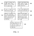
- FIG. 4 is a flowchart illustrating a package process according to another embodiment of the present application.
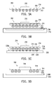
- FIGs. 5A-5F are diagrams sequentially illustrating steps of a package process of FIG. 4 .
- FIG. 6 is a top view of a POP structure according to an embodiment of the present application.
- an insulation paste having a liquid state or a semi-solid state is first coated on conductive bumps, and after the electronic component is mounted, the insulation paste is cured while the conductive bumps are reflowed.
- only one heating process is performed to reflow the conductive bumps and cure the insulation paste simultaneously, wherein a temperature of the heating process is controlled within a range that the conductive bumps may have a melted state or a semi-melted state.
- a material of the conductive bumps can be a lead-free solder, and the temperature of the heating process is, for example, between 200°C and 260 °C.
- the package process of the present application can be applied to a package structure with a single electronic component, or can be applied to a package on package (POP) structure.
- the aforementioned heating process used for curing the insulation paste and reflowing the conductive bumps can be used to bond the electronic component to a circuit substrate, and can also be used to bond the electronic components of the POP structure.
- Embodiments are provided below to describe the package process and the package structure of the present application.
- FIG. 1 is a flowchart illustrating a package process according to an embodiment of the present application.
- FIGs. 2A-2D are diagrams sequentially illustrating steps of a package process of FIG. 1 .
- a first electronic component 210 is provided, the first electronic component 210 has a plurality of first conductive bumps 212 at a bottom thereof.
- the first electronic component 210 is, for example, a packaged central processing unit (CPU) including a first carrier 214 and a first chip 216 located on the first carrier 214.
- the first conductive bumps 212 are located on the bottom of the first carrier 214, and the first conductive bumps 212 are, for example, ball-shape solder bumps arranged in an array, and are formed on a plurality of solder pads 218 on the bottom of the first carrier 214, so as to be electrically connected to the first chip 216 through the first carrier 214.
- the first conductive bumps 212 are, for example, lead-free tin balls.
- a first insulation paste 220 is coated on the first conductive bumps 212.
- the first conductive bumps 212 of the first electronic component 210 are, for example, disposed in insulation paste solution 720 contained by a container 710 according to a dipping method, so that each of the first conductive bumps 212 is coated by the first insulation paste 220.
- An advantage of the dipping method is that the processing is simple and quick.
- the method for coating the first insulation paste 220 on the first conductive bumps 212 is not limited thereto, and those with ordinary skill in the art can apply other methods such as printing and spraying, etc. to form the first insulation paste 220 on the first conductive bumps 212 according to an actual demand.
- the first electronic component 210 is disposed on a circuit substrate 230.
- a carrying surface 230a of the circuit substrate 230 has a plurality of substrate pads 232 corresponding to the first conductive bumps 212.
- the first electronic component 210 is disposed on the carrying surface 230a, and the first conductive bumps 212 are respectively situated on the substrate pads 232.
- a pre-solder 234 can be formed on each of the substrate pads 232 to improve a bonding effect of the first conductive bumps 212 in a follow-up process.
- the pre-solder 234 is, for example, a solder paste formed by printing.
- a heating process is performed to both of the first conductive bumps 212 and the first insulation paste 220 to reflow the first conductive bumps 212 and cure the first insulation paste 220.
- the first conductive bumps 212 may have a melted state or a semi-melted state when being reflowed, so as to be respectively bonded to the solder pads 218 on the bottom of the first electronic component 210 and the substrate pads 232 of the circuit substrate 230, and the first conductive bumps 212 are connected to the solder pads 218 and the corresponding substrate pads 232 after being cooled down.
- the first conductive bumps 212 can be respectively integrated with the corresponding pre-solders 234 when being reflowed.
- the first insulation paste 220 is filled in spaces among the first conductive bumps 212 for wrapping the first conductive bumps 212, and is cured during the heating process.
- the first insulation paste 220 is not limited to be filled in the spaces among the first conductive bumps 212, i.e. the first insulation paste 220 can be only filled in a part of the spaces among the first conductive bumps 212 without totally wrapping the first conductive bumps 212.
- internal of the first insulation paste 220 probably contains air bubbles.
- a temperature of the heating process is determined according to materials of the first conductive bumps 212 and the first insulation paste 220. Since a melting point of the first conductive bump 212 is generally higher than a curing temperature of the first insulation paste 220, the temperature of the heating process is required to be higher than the melting point of the first conductive bumps 212.
- the material of the first conductive bumps 212 is, for example, a lead-free solder, and the temperature of the heating process is, for example, between 200°C and 260°C.
- the first insulation paste 220 is first coated on the first conductive bumps 212, and after the first electronic component 210 is bonded to the circuit substrate 230, only one heating process is performed to complete reflowing the first conductive bumps 212 and curing the first insulation paste 220.
- the first conductive bumps 212 for example, maintain a solid state before the heating process, and the first conductive bumps 212 are bonded to the first electronic component 210 and the circuit substrate 230 when the heating process is performed.
- FIG. 3 is a top view of the aforementioned package structure.
- the first insulation paste 220 is formed on the first conductive bumps 212 before the first electronic component 210 is bonded to the circuit substrate 230, after the first electronic component 210 is bonded to the circuit substrate 230, and the heating process is performed, the first insulation paste 220 can enter spaces among the first conductive bumps 212 without being exposed outside the first electronic component 210.
- the first electronic component 210 has a first vertical projection region R1 on the circuit substrate 230, and the first insulation paste 220 is located within the first vertical projection region R1. Therefore, a problem of remaining the underfill outside the electronic component due to a conventional dispensing step can be resolved, so that the appearance of the package structure can be greatly improved.
- the POP package process can also be simplified according to the present application.
- FIG. 4 is a flowchart illustrating a package process according to another embodiment of the present application.
- FIGs. 5A-5F are diagrams sequentially illustrating steps of the package process of FIG. 4 .
- the first electronic component 210 is provided (referring to FIG. 5A ), the first insulation paste 220 is coated on the first conductive bumps 212 located at the bottom of the first electronic component 210 (referring to FIG. 5B ), and the first electronic component 210 is disposed on the circuit substrate 230 (referring to FIG. 5C ). Since the above steps are similar to that of the aforementioned embodiment, same reference numerals are used to denote the steps and the devices, and related technical descriptions are not repeated. Though, since a second electronic component is required to be stacked on the first electronic component 210 in the present embodiment, the first electronic component 210 further has a plurality of first pads 219 for bonding the second electronic component.
- the present embodiment provides a second electronic component 510.
- the second electronic component 510 has a plurality of second conductive bumps 512 at a bottom thereof.
- the second electronic component 510 is, for example, a packaged memory unit including a second carrier 514 and a second chip 516 located on the second carrier 514.
- the second conductive bumps 512 are located on the bottom of the second carrier 514, and the second conductive bumps 512 are, for example, ball-shape solder bumps arranged in an array, and are formed on a plurality of solder pads 518 on the bottom of the second carrier 514, so as to be electrically connected to the second chip 516 through the second carrier 514.
- the second conductive bumps 512 are, for example, lead-free tin balls.
- a second insulation paste 520 is coated on the second conductive bumps 512.
- the second conductive bumps 512 of the second electronic component 510 are, for example, disposed in insulation paste solution 820 contained by a container 810 according to the dipping method, so that each of the second conductive bumps 512 is coated by the second insulation paste 520.
- a material of the second insulation paste 520 can be the same or different to that of the first insulation paste 220 to meet different design requirements. For example, a material cost can be reduced, and setting of process parameters can be simplified by using the same material, while effects for buffering stress at the junction and strengthening a bonding strength can be achieved by using different materials.
- the second electronic component 510 is disposed on the first electronic component 210, wherein the second conductive bumps 512 are respectively situated on the first pads 219.
- a heating process is simultaneously performed to the first conductive bumps 212, the first insulation paste 220, the second conductive bumps 512 and the second insulation paste 520 to reflow the first conductive bumps 212 and the second conductive bumps 512, and cure the first insulation paste 220 and the second insulation paste 520.
- the first conductive bumps 212 may have a melted state or a semi-melted state when being reflowed, so as to be respectively bonded to the solder pads 218 on the bottom of the first electronic component 210 and the substrate pads 232 of the circuit substrate 230, and the first conductive bumps 212 are connected to the solder pads 218 and the corresponding substrate pads 232 after being cooled down.
- the pre-solder 234 is first formed on each of the substrate pads 232, the first conductive bumps 212 can be respectively integrated with the corresponding pre-solders 234 when being reflowed.
- the second conductive bumps 512 may have the melted state or the semi-melted state when being reflowed, so as to be respectively bonded to the solder pads 518 on the bottom of the second electronic component 510 and the first pads 219 on the top of the first electronic component 210, and the second conductive bumps 512 are connected to the solder pads 518 and the corresponding first pads 219 after being cooled down.
- the first insulation paste 220 enters the spaces among the first conductive bumps 212, and is cured during the heating process.
- the second insulation paste 520 enters the spaces among the second conductive bumps 512 for wrapping the second conductive bumps 512, and is cured during the heating process.
- the second insulation paste 520 is not limited to be filled in the spaces among the second conductive bumps 512, i.e. the second insulation paste 520 can be only filled in a part of the spaces among the second conductive bumps 512 without totally wrapping the second conductive bumps 512.
- internal of the second insulation paste 520 probably contains air bubbles.
- a temperature of the heating process is determined according to materials of the first conductive bumps 212, the second conductive bumps 512, the first insulation paste 220 and the second insulation paste 520. Since the melting point of the first conductive bumps 212 is generally higher than the curing temperature of the first insulation paste 220, and a melting point of the second conductive bumps 512 is generally higher than a curing temperature of the second insulation paste 520, the temperature of the heating process is required to be higher than the melting points of the first conductive bumps 212 and the second conductive bumps 512.
- the materials of the first conductive bumps 212 and the second conductive bumps 512 are, for example, the lead-free solder, and the temperature of the heating process is, for example, between 200°C and 260°C.
- the first insulation paste 220 is first coated on the first conductive bumps 212
- the second insulation paste 520 is first coated on the second conductive bumps 512.
- FIG. 6 is a top view of the POP structure of the aforementioned embodiment.
- the second insulation paste 520 is formed on the second conductive bumps 212 before the second electronic component 510 is bonded to the first electronic component 210, after the second electronic component 510 is bonded to the first electronic component 210, and the heating process is performed, the second insulation paste 520 can enter the spaces among the second conductive bumps 512 without being exposed outside the second electronic component 510.
- the second electronic component 510 has a second vertical projection region R2 on the first electronic component 210, and the second insulation paste 520 is located within the second vertical projection region R2.
- FIG. 6 is a top view of the POP structure of the aforementioned embodiment.
- the first insulation paste 220 can enter the spaces among the first conductive bumps 212 without being exposed outside the first electronic component 210.
- the first electronic component 210 has a first vertical projection region R on the circuit substrate 230, and the first insulation paste 220 is located within the first vertical projection region R. Therefore, a problem of remaining the underfill outside the electronic component due to the conventional dispensing step can be resolved, so that the appearance of the package structure can be greatly improved.
- the package process of the present application has simple steps to avoid the problem of poor production yield caused by complicated process steps, but also process equipments, materials and labour cost can be reduced to improve the production yield and the production efficiency.
- a problem of exposing the underfill in the conventional technique can be resolved, so that the package structure may have a better appearance.
Landscapes
- Engineering & Computer Science (AREA)
- Manufacturing & Machinery (AREA)
- Microelectronics & Electronic Packaging (AREA)
- Wire Bonding (AREA)
- Electric Connection Of Electric Components To Printed Circuits (AREA)
Abstract
A package structure and a package process are provided. In the package process, firstly, a first electronic component having a plurality of first conductive bumps at a bottom thereof is provided. Then, a first insulation paste is coated on the first conductive bumps. The first electronic component is disposed on a circuit substrate having a plurality of substrate pads, and the first conductive bumps are respectively situated on the substrate pads. Next, a heating process is performed to both of the first conductive bumps and the first insulation paste, wherein the first conductive bumps is reflowed to bond the first electronic component and the substrate pads, and the first insulation paste is cured.
Description
- The present application relates to a package structure and a fabrication method thereof. More particularly, the present application relates to a package structure integrating curing of an insulation paste and reflow of conductive bumps in a same heating process, and a fabrication method thereof.
- Recently, with quick development of the integrated circuit (IC) technique and material technique, a size of a chip in the IC is gradually reduced, though a function thereof is increasingly improved, so that application of the IC technique is widespread. Therefore, products, such as handheld electronic devices, electronic dictionaries, digital cameras and various digital products, etc., manufactured according to the IC technique have a general trend of lightness, slimness, shortness and smallness.
- The surface mounting technology (SMT) is a commonly used technique for mounting an electronic component or other components to a circuit board. According to the SMT, a size of a whole package structure can be reduced, which avails miniaturization of an electronic apparatus.
- According to the known SMT, a reflow step is performed to conductive bumps between the electronic component and the circuit board after the electronic component is mounted to the circuit board, so that the conductive bumps may have a melted state or a semi-melted state to bond the electronic component and the circuit board. Then, an underfill is filled between the electronic component and the circuit board, and a curing step is performed to the underfill. Generally, a reflow temperature of the conductive bumps is required to be higher than a melting point of the conductive bumps, and a heating temperature for curing the underfill is far lower than the reflow temperature of the conductive bumps.
- However, according to the known SMT, after the conductive bumps are reflowed, an underfill process is further performed, and steps thereof are quite complicated, which may influence a production yield. Moreover, since a fabrication condition of curing the underfill is different to a fabrication condition of reflowing the conductive bumps, two fabrication equipments have to be used, which may increase a production cost.
- On the other hand, according to the known SMT, a method of forming the underfill is that after the electronic component is mounted to the circuit board, a dispensing step is performed outside a junction of the electronic component and the circuit board, so that the underfill can enter a space between the electronic component and the circuit board to wrap the conductive bumps according to a siphon phenomenon. Though, a part of the underfill is remained outside the electronic component according to such dispensing method, which may influence an appearance of the package structure.
- The present application is directed to a package process, which has simple process steps, so that production efficiency can be improved.
- The present application is directed to a package structure, which can avoid exposing an underfill, so that an appearance of a product is improved.
- The present application provides a package process. First, a first electronic component having a plurality of first conductive bumps at a bottom thereof is provided. Next, a first insulation paste is coated on the first conductive bumps. Next, the first electronic component is disposed on a circuit substrate having a plurality of substrate pads, and the first conductive bumps are respectively situated on the substrate pads. Next, a heating process is performed to both of the first conductive bumps and the first insulation paste, so that the first conductive bumps are reflowed to bond the first electronic component and the substrate pads, and the first insulation paste is cured.
- The present application further provides a package structure including a circuit substrate, a first electronic component, a plurality of first conductive bumps and a first insulation paste. The circuit substrate has a plurality of substrate pads, and the first electronic component is disposed on the circuit substrate. The first conductive bumps are disposed between the first electronic component and the circuit substrate, wherein each of the first conductive bumps is connected to the first electronic component and the corresponding substrate pad. The first insulation paste is disposed between the first electronic component and the circuit substrate. Moreover, the first electronic component has a first vertical projection region on the circuit substrate, and the first insulation paste is located in the first vertical projection region.
- According to the package process of the present application, the conductive bumps are reflowed and the insulation paste is cured by performing a same heating process. Comparing to a conventional technique forming the underfill after the electronic component is mounted, the package process of the present application is simple, and therefore a problem of poor production yield caused by complicated process steps can be avoided, and process equipments, materials and labour cost can be reduced to improve production efficiency. On the other hand, since the package process forms the insulation paste on the conductive bumps before the electronic component is mounted, the insulation paste is not exposed outside the electronic component after the electronic component is mounted and the heating process is performed, so that the package structure may have a better appearance.
- In order to make the aforementioned and other features and advantages of the present application comprehensible, several exemplary embodiments accompanied with figures are described in detail below.
- The accompanying drawings are included to provide a further understanding of the application, and are incorporated in and constitute a part of this specification. The drawings illustrate embodiments of the application and, together with the description, serve to explain the principles of the application.
-
FIG. 1 is a flowchart illustrating a package process according to an embodiment of the present application. -
FIGs. 2A-2D are diagrams sequentially illustrating steps of a package process ofFIG. 1 . -
FIG. 3 is a top view of a package structure according to an embodiment of the present application. -
FIG. 4 is a flowchart illustrating a package process according to another embodiment of the present application. -
FIGs. 5A-5F are diagrams sequentially illustrating steps of a package process ofFIG. 4 . -
FIG. 6 is a top view of a POP structure according to an embodiment of the present application. - In the present application, before an electronic component is mounted, an insulation paste having a liquid state or a semi-solid state is first coated on conductive bumps, and after the electronic component is mounted, the insulation paste is cured while the conductive bumps are reflowed. In other words, in the present application, only one heating process is performed to reflow the conductive bumps and cure the insulation paste simultaneously, wherein a temperature of the heating process is controlled within a range that the conductive bumps may have a melted state or a semi-melted state. For example, a material of the conductive bumps can be a lead-free solder, and the temperature of the heating process is, for example, between 200°C and 260 °C.
- Moreover, the package process of the present application can be applied to a package structure with a single electronic component, or can be applied to a package on package (POP) structure. In other words, the aforementioned heating process used for curing the insulation paste and reflowing the conductive bumps can be used to bond the electronic component to a circuit substrate, and can also be used to bond the electronic components of the POP structure.
- Embodiments are provided below to describe the package process and the package structure of the present application.
-
FIG. 1 is a flowchart illustrating a package process according to an embodiment of the present application.FIGs. 2A-2D are diagrams sequentially illustrating steps of a package process ofFIG. 1 . - First, as shown in
step 110 andFIG. 2A , a firstelectronic component 210 is provided, the firstelectronic component 210 has a plurality of firstconductive bumps 212 at a bottom thereof. Here, the firstelectronic component 210 is, for example, a packaged central processing unit (CPU) including afirst carrier 214 and afirst chip 216 located on thefirst carrier 214. The firstconductive bumps 212 are located on the bottom of thefirst carrier 214, and the firstconductive bumps 212 are, for example, ball-shape solder bumps arranged in an array, and are formed on a plurality ofsolder pads 218 on the bottom of thefirst carrier 214, so as to be electrically connected to thefirst chip 216 through thefirst carrier 214. Here, the firstconductive bumps 212 are, for example, lead-free tin balls. - Next, as shown in
step 120 andFIG. 2B , afirst insulation paste 220 is coated on the firstconductive bumps 212. In the present embodiment, the firstconductive bumps 212 of the firstelectronic component 210 are, for example, disposed ininsulation paste solution 720 contained by acontainer 710 according to a dipping method, so that each of the firstconductive bumps 212 is coated by thefirst insulation paste 220. An advantage of the dipping method is that the processing is simple and quick. Certainly, the method for coating thefirst insulation paste 220 on the firstconductive bumps 212 is not limited thereto, and those with ordinary skill in the art can apply other methods such as printing and spraying, etc. to form thefirst insulation paste 220 on the firstconductive bumps 212 according to an actual demand. - Next, as shown in
step 130 andFIG. 2C , the firstelectronic component 210 is disposed on acircuit substrate 230. In the present embodiment, a carryingsurface 230a of thecircuit substrate 230 has a plurality ofsubstrate pads 232 corresponding to the firstconductive bumps 212. The firstelectronic component 210 is disposed on the carryingsurface 230a, and the firstconductive bumps 212 are respectively situated on thesubstrate pads 232. In the present embodiment, before thestep 130, a pre-solder 234 can be formed on each of thesubstrate pads 232 to improve a bonding effect of the firstconductive bumps 212 in a follow-up process. The pre-solder 234 is, for example, a solder paste formed by printing. - Next, as shown in
step 140 andFIG. 2D , a heating process is performed to both of the firstconductive bumps 212 and thefirst insulation paste 220 to reflow the firstconductive bumps 212 and cure thefirst insulation paste 220. The firstconductive bumps 212 may have a melted state or a semi-melted state when being reflowed, so as to be respectively bonded to thesolder pads 218 on the bottom of the firstelectronic component 210 and thesubstrate pads 232 of thecircuit substrate 230, and the firstconductive bumps 212 are connected to thesolder pads 218 and thecorresponding substrate pads 232 after being cooled down. Moreover, as describe above, if the pre-solder 234 is first formed on each of thesubstrate pads 232, the firstconductive bumps 212 can be respectively integrated with thecorresponding pre-solders 234 when being reflowed. On the other hand, after the firstelectronic component 210 is bonded to thecircuit substrate 230, thefirst insulation paste 220 is filled in spaces among the firstconductive bumps 212 for wrapping the firstconductive bumps 212, and is cured during the heating process. However, thefirst insulation paste 220 is not limited to be filled in the spaces among the firstconductive bumps 212, i.e. thefirst insulation paste 220 can be only filled in a part of the spaces among the firstconductive bumps 212 without totally wrapping the firstconductive bumps 212. Furthermore, in an actual package process, internal of thefirst insulation paste 220 probably contains air bubbles. - During the actual package process, a temperature of the heating process is determined according to materials of the first
conductive bumps 212 and thefirst insulation paste 220. Since a melting point of the firstconductive bump 212 is generally higher than a curing temperature of thefirst insulation paste 220, the temperature of the heating process is required to be higher than the melting point of the firstconductive bumps 212. In the present embodiment, the material of the firstconductive bumps 212 is, for example, a lead-free solder, and the temperature of the heating process is, for example, between 200°C and 260°C. - In the present embodiment, before the first
electronic component 210 is bonded to thecircuit substrate 230, thefirst insulation paste 220 is first coated on the firstconductive bumps 212, and after the firstelectronic component 210 is bonded to thecircuit substrate 230, only one heating process is performed to complete reflowing the firstconductive bumps 212 and curing thefirst insulation paste 220. In other words, the firstconductive bumps 212, for example, maintain a solid state before the heating process, and the firstconductive bumps 212 are bonded to the firstelectronic component 210 and thecircuit substrate 230 when the heating process is performed. - In the package process of the present embodiment, only one heating process is performed to reflow the conductive bumps and cure the insulation paste, so that process steps can be simplified to reduce a problem of poor production yield, and process equipments, materials and labour cost can be reduced to improve production efficiency.
-
FIG. 3 is a top view of the aforementioned package structure. As shown inFIG. 3 , since in the package structure formed according to the aforementioned package process, thefirst insulation paste 220 is formed on the firstconductive bumps 212 before the firstelectronic component 210 is bonded to thecircuit substrate 230, after the firstelectronic component 210 is bonded to thecircuit substrate 230, and the heating process is performed, thefirst insulation paste 220 can enter spaces among the firstconductive bumps 212 without being exposed outside the firstelectronic component 210. In other words, the firstelectronic component 210 has a first vertical projection region R1 on thecircuit substrate 230, and thefirst insulation paste 220 is located within the first vertical projection region R1. Therefore, a problem of remaining the underfill outside the electronic component due to a conventional dispensing step can be resolved, so that the appearance of the package structure can be greatly improved. - Based on the aforementioned embodiment, the POP package process can also be simplified according to the present application.
-
FIG. 4 is a flowchart illustrating a package process according to another embodiment of the present application.FIGs. 5A-5F are diagrams sequentially illustrating steps of the package process ofFIG. 4 . - First, as described in the steps 110-130 of the aforementioned embodiment, the first
electronic component 210 is provided (referring toFIG. 5A ), thefirst insulation paste 220 is coated on the firstconductive bumps 212 located at the bottom of the first electronic component 210 (referring toFIG. 5B ), and the firstelectronic component 210 is disposed on the circuit substrate 230 (referring toFIG. 5C ). Since the above steps are similar to that of the aforementioned embodiment, same reference numerals are used to denote the steps and the devices, and related technical descriptions are not repeated. Though, since a second electronic component is required to be stacked on the firstelectronic component 210 in the present embodiment, the firstelectronic component 210 further has a plurality offirst pads 219 for bonding the second electronic component. - As shown in
step 410 andFIG. 5D , the present embodiment provides a secondelectronic component 510. The secondelectronic component 510 has a plurality of secondconductive bumps 512 at a bottom thereof. Here, the secondelectronic component 510 is, for example, a packaged memory unit including asecond carrier 514 and asecond chip 516 located on thesecond carrier 514. The secondconductive bumps 512 are located on the bottom of thesecond carrier 514, and the secondconductive bumps 512 are, for example, ball-shape solder bumps arranged in an array, and are formed on a plurality ofsolder pads 518 on the bottom of thesecond carrier 514, so as to be electrically connected to thesecond chip 516 through thesecond carrier 514. Here, the secondconductive bumps 512 are, for example, lead-free tin balls. - Moreover, as shown in
step 420 andFIG. 5D , asecond insulation paste 520 is coated on the secondconductive bumps 512. In the present embodiment, the secondconductive bumps 512 of the secondelectronic component 510 are, for example, disposed ininsulation paste solution 820 contained by acontainer 810 according to the dipping method, so that each of the secondconductive bumps 512 is coated by thesecond insulation paste 520. A material of thesecond insulation paste 520 can be the same or different to that of thefirst insulation paste 220 to meet different design requirements. For example, a material cost can be reduced, and setting of process parameters can be simplified by using the same material, while effects for buffering stress at the junction and strengthening a bonding strength can be achieved by using different materials. - Next, as shown in
step 430 andFIG. 5E , the secondelectronic component 510 is disposed on the firstelectronic component 210, wherein the secondconductive bumps 512 are respectively situated on thefirst pads 219. - Next, as shown in
step 440 andFIG. 5F , a heating process is simultaneously performed to the firstconductive bumps 212, thefirst insulation paste 220, the secondconductive bumps 512 and thesecond insulation paste 520 to reflow the firstconductive bumps 212 and the secondconductive bumps 512, and cure thefirst insulation paste 220 and thesecond insulation paste 520. The firstconductive bumps 212 may have a melted state or a semi-melted state when being reflowed, so as to be respectively bonded to thesolder pads 218 on the bottom of the firstelectronic component 210 and thesubstrate pads 232 of thecircuit substrate 230, and the firstconductive bumps 212 are connected to thesolder pads 218 and thecorresponding substrate pads 232 after being cooled down. Moreover, as described above, if the pre-solder 234 is first formed on each of thesubstrate pads 232, the firstconductive bumps 212 can be respectively integrated with thecorresponding pre-solders 234 when being reflowed. - The second
conductive bumps 512 may have the melted state or the semi-melted state when being reflowed, so as to be respectively bonded to thesolder pads 518 on the bottom of the secondelectronic component 510 and thefirst pads 219 on the top of the firstelectronic component 210, and the secondconductive bumps 512 are connected to thesolder pads 518 and the correspondingfirst pads 219 after being cooled down. - On the other hand, as described in the aforementioned embodiment, after the first
electronic component 210 is bonded to thecircuit substrate 230, thefirst insulation paste 220 enters the spaces among the firstconductive bumps 212, and is cured during the heating process. - Moreover, after the second
electronic component 510 is bonded to the firstelectronic component 210, thesecond insulation paste 520 enters the spaces among the secondconductive bumps 512 for wrapping the secondconductive bumps 512, and is cured during the heating process. Similarly, thesecond insulation paste 520 is not limited to be filled in the spaces among the secondconductive bumps 512, i.e. thesecond insulation paste 520 can be only filled in a part of the spaces among the secondconductive bumps 512 without totally wrapping the secondconductive bumps 512. Alternatively, in an actual package process, internal of thesecond insulation paste 520 probably contains air bubbles. - During the actual package process, a temperature of the heating process is determined according to materials of the first
conductive bumps 212, the secondconductive bumps 512, thefirst insulation paste 220 and thesecond insulation paste 520. Since the melting point of the firstconductive bumps 212 is generally higher than the curing temperature of thefirst insulation paste 220, and a melting point of the secondconductive bumps 512 is generally higher than a curing temperature of thesecond insulation paste 520, the temperature of the heating process is required to be higher than the melting points of the firstconductive bumps 212 and the secondconductive bumps 512. In the present embodiment, the materials of the firstconductive bumps 212 and the secondconductive bumps 512 are, for example, the lead-free solder, and the temperature of the heating process is, for example, between 200°C and 260°C. - In the present embodiment, before the first
electronic component 210 is bonded to thecircuit substrate 230, thefirst insulation paste 220 is first coated on the firstconductive bumps 212, and before the secondelectronic component 510 is bonded to the firstelectronic component 210, thesecond insulation paste 520 is first coated on the secondconductive bumps 512. After the firstelectronic component 210 is bonded to thecircuit substrate 230, and the secondelectronic component 510 is bonded to the firstelectronic component 210, only one heating process is performed to complete reflowing the firstconductive bumps 212 and the secondconductive bumps 512, and curing thefirst insulation paste 220 and thesecond insulation paste 520. In other words, the firstconductive bumps 212 and the secondconductive bumps 512, for example, maintain the solid state before the heating process, and are changed into the melted state or the semi-melted state when the heating process is performed. - In the POP package process of the present embodiment, only one heating process is performed to reflow all of the conductive bumps and cure all of the insulation paste, so that process steps can be simplified to reduce a problem of poor production yield, and process equipments, materials and labour cost can be reduced to improve production efficiency.
-
FIG. 6 is a top view of the POP structure of the aforementioned embodiment. As shown inFIG. 6 , since in the package structure formed according to the aforementioned package process, thesecond insulation paste 520 is formed on the secondconductive bumps 212 before the secondelectronic component 510 is bonded to the firstelectronic component 210, after the secondelectronic component 510 is bonded to the firstelectronic component 210, and the heating process is performed, thesecond insulation paste 520 can enter the spaces among the secondconductive bumps 512 without being exposed outside the secondelectronic component 510. In other words, the secondelectronic component 510 has a second vertical projection region R2 on the firstelectronic component 210, and thesecond insulation paste 520 is located within the second vertical projection region R2. Similarly, referring toFIG. 3 , thefirst insulation paste 220 can enter the spaces among the firstconductive bumps 212 without being exposed outside the firstelectronic component 210. In other words, the firstelectronic component 210 has a first vertical projection region R on thecircuit substrate 230, and thefirst insulation paste 220 is located within the first vertical projection region R. Therefore, a problem of remaining the underfill outside the electronic component due to the conventional dispensing step can be resolved, so that the appearance of the package structure can be greatly improved. - In summary, not only the package process of the present application has simple steps to avoid the problem of poor production yield caused by complicated process steps, but also process equipments, materials and labour cost can be reduced to improve the production yield and the production efficiency. Moreover, regarding the package structure of the present application, a problem of exposing the underfill in the conventional technique can be resolved, so that the package structure may have a better appearance.
- It will be apparent to those skilled in the art that various modifications and variations can be made to the structure of the present application without departing from the scope or spirit of the application. In view of the foregoing, it is intended that the present application cover modifications and variations of this application provided they fall within the scope of the following claims and their equivalents.
Claims (10)
- A package process, comprising:providing a first electronic component (210), and the first electronic component having a plurality of first conductive bumps (212) on a bottom thereof;coating a first insulation paste (220) on the first conductive bumps;disposing the first electronic component on a circuit substrate (230) having a plurality of substrate pads (232), and the first conductive bumps being respectively situated on the substrate pads; andperforming a heating process to both of the first conductive bumps and the first insulation paste, so that the first conductive bumps are reflowed to bond the first electronic component and the corresponding substrate pads, and the first insulation paste is cured.
- The package process as claimed in claim 1, wherein the first conductive bumps maintain a solid state before the heating process is performed.
- The package process as claimed in claim 2, wherein a temperature of the heating process is between 200 °C and 260°C.
- The package process as claimed in claim 1, further comprising following steps before the heating process is performed:providing a second electronic (510) component, and the second electronic component has a plurality of second conductive bumps (512) on a bottom thereof;coating a second insulation paste (520) on the second conductive bumps; anddisposing the second electronic component on the first electronic component, wherein the first electronic component has a plurality of first pads, and the second conductive bumps are respectively situated on the first pads.
- The package process as claimed in claim 4, wherein the heating process is performed to further both of the second conductive bumps and the second insulation paste, so that the second conductive bumps are reflowed to bond the second electronic component and the corresponding second pads, and the second insulation paste is cured.
- The package process as claimed in claim 5, wherein the second conductive bumps maintain a solid state before the heating process is performed.
- The package process as claimed in claim 6, wherein a temperature of the heating process is between 200°C and 260°C.
- The package process as claimed in claim 1, further comprising forming a pre-solder on each of the substrate pads before the first electronic component is disposed on the circuit substrate, so that after the first conductive bumps are reflowed, the first conductive bumps are respectively integrated with the corresponding pre-solders.
- A package structure, comprising:a circuit substrate (230), having a plurality of substrate pads (232);a first electronic component (210), disposed on the circuit substrate;a plurality of first conductive bumps (212), each of the first conductive bumps being connected to the first electronic component and the corresponding substrate pad; anda first insulation paste (220), disposed between the first electronic component and the circuit substrate, the first electronic component having a first vertical projection region on the circuit substrate, and the first insulation paste being located in the first vertical projection region.
- The package structure as claimed in claim 9, further comprising:a second electronic component (510), disposed on the first electronic component, and the first electronic component having a plurality of first pad;a plurality of second conductive bumps, each of the second conductive bumps (512) being connected to the second electronic component and the corresponding first pad; anda second insulation paste (520), disposed between the second electronic component and the first electronic component, the second electronic component having a second vertical projection region on the first electronic component, and the second insulation paste being located in the second vertical projection region.
Applications Claiming Priority (1)
| Application Number | Priority Date | Filing Date | Title |
|---|---|---|---|
| TW098126532A TWI478257B (en) | 2009-08-06 | 2009-08-06 | Package structure and packaging process |
Publications (1)
| Publication Number | Publication Date |
|---|---|
| EP2284880A1 true EP2284880A1 (en) | 2011-02-16 |
Family
ID=42312131
Family Applications (1)
| Application Number | Title | Priority Date | Filing Date |
|---|---|---|---|
| EP10150506A Ceased EP2284880A1 (en) | 2009-08-06 | 2010-01-12 | Package structure and package process |
Country Status (3)
| Country | Link |
|---|---|
| US (1) | US8697489B2 (en) |
| EP (1) | EP2284880A1 (en) |
| TW (1) | TWI478257B (en) |
Cited By (1)
| Publication number | Priority date | Publication date | Assignee | Title |
|---|---|---|---|---|
| WO2014052273A1 (en) * | 2012-09-26 | 2014-04-03 | Apple Inc. | PoP STRUCTURE WITH ELECTRICALLY INSULATING MATERIAL BETWEEN PACKAGES |
Families Citing this family (3)
| Publication number | Priority date | Publication date | Assignee | Title |
|---|---|---|---|---|
| US9263377B2 (en) | 2012-11-08 | 2016-02-16 | Taiwan Semiconductor Manufacturing Company, Ltd. | POP structures with dams encircling air gaps and methods for forming the same |
| US9016552B2 (en) * | 2013-03-15 | 2015-04-28 | Sanmina Corporation | Method for forming interposers and stacked memory devices |
| CN113019729B (en) * | 2021-03-11 | 2022-04-22 | 深圳市德贝尔喷枪有限公司 | High-voltage package structure of powder electrostatic spray gun and packaging process thereof |
Citations (3)
| Publication number | Priority date | Publication date | Assignee | Title |
|---|---|---|---|---|
| US20040232210A1 (en) * | 2003-05-23 | 2004-11-25 | Jayesh Shah | Pre-applied fluxing underfill composition having pressure sensitive adhesive properties |
| US20070170599A1 (en) * | 2006-01-24 | 2007-07-26 | Masazumi Amagai | Flip-attached and underfilled stacked semiconductor devices |
| US20070170586A1 (en) * | 2006-01-23 | 2007-07-26 | Samsung Electro-Mechanics Co., Ltd | Printed circuit board for semiconductor package and method of manufacturing the same |
Family Cites Families (10)
| Publication number | Priority date | Publication date | Assignee | Title |
|---|---|---|---|---|
| JP2001510944A (en) * | 1997-07-21 | 2001-08-07 | アギラ テクノロジーズ インコーポレイテッド | Semiconductor flip chip package and method of manufacturing the same |
| JP3625268B2 (en) * | 2000-02-23 | 2005-03-02 | 富士通株式会社 | Mounting method of semiconductor device |
| US6420216B1 (en) | 2000-03-14 | 2002-07-16 | International Business Machines Corporation | Fuse processing using dielectric planarization pillars |
| JP2001352035A (en) * | 2000-06-07 | 2001-12-21 | Sony Corp | Assembly jig for multilayer semiconductor device and method for manufacturing multilayer semiconductor device |
| US6610559B2 (en) * | 2001-11-16 | 2003-08-26 | Indium Corporation Of America | Integrated void-free process for assembling a solder bumped chip |
| JP3875077B2 (en) * | 2001-11-16 | 2007-01-31 | 富士通株式会社 | Electronic device and device connection method |
| US6906425B2 (en) * | 2002-03-05 | 2005-06-14 | Resolution Performance Products Llc | Attachment of surface mount devices to printed circuit boards using a thermoplastic adhesive |
| TWI229928B (en) * | 2003-08-19 | 2005-03-21 | Advanced Semiconductor Eng | Semiconductor package structure |
| TWI237370B (en) * | 2004-07-30 | 2005-08-01 | Advanced Semiconductor Eng | Chip package structure and process for fabricating the same |
| US7843074B2 (en) * | 2006-09-12 | 2010-11-30 | Lumination Llc | Underfill for light emitting device |
-
2009
- 2009-08-06 TW TW098126532A patent/TWI478257B/en active
- 2009-12-11 US US12/635,701 patent/US8697489B2/en active Active
-
2010
- 2010-01-12 EP EP10150506A patent/EP2284880A1/en not_active Ceased
Patent Citations (3)
| Publication number | Priority date | Publication date | Assignee | Title |
|---|---|---|---|---|
| US20040232210A1 (en) * | 2003-05-23 | 2004-11-25 | Jayesh Shah | Pre-applied fluxing underfill composition having pressure sensitive adhesive properties |
| US20070170586A1 (en) * | 2006-01-23 | 2007-07-26 | Samsung Electro-Mechanics Co., Ltd | Printed circuit board for semiconductor package and method of manufacturing the same |
| US20070170599A1 (en) * | 2006-01-24 | 2007-07-26 | Masazumi Amagai | Flip-attached and underfilled stacked semiconductor devices |
Non-Patent Citations (1)
| Title |
|---|
| LI LI ET AL: "Pb-free solder paste reflow window study for flip chip wafer bumping", ADVANCED PACKAGING MATERIALS: PROCESSES, PROPERTIES AND INTERFACES, 20 01. PROCEEDINGS. INTERNATIONAL SYMPOSIUM ON MARCH 11-14, 2001, PISCATAWAY, NJ, USA,IEEE, 11 March 2001 (2001-03-11), pages 112 - 118, XP010539031, ISBN: 978-0-930815-64-6, DOI: 10.1109/ISAOM.2001.916559 * |
Cited By (3)
| Publication number | Priority date | Publication date | Assignee | Title |
|---|---|---|---|---|
| WO2014052273A1 (en) * | 2012-09-26 | 2014-04-03 | Apple Inc. | PoP STRUCTURE WITH ELECTRICALLY INSULATING MATERIAL BETWEEN PACKAGES |
| US8963311B2 (en) | 2012-09-26 | 2015-02-24 | Apple Inc. | PoP structure with electrically insulating material between packages |
| US9263426B2 (en) | 2012-09-26 | 2016-02-16 | Apple Inc. | PoP structure with electrically insulating material between packages |
Also Published As
| Publication number | Publication date |
|---|---|
| TW201106435A (en) | 2011-02-16 |
| TWI478257B (en) | 2015-03-21 |
| US20110031605A1 (en) | 2011-02-10 |
| US8697489B2 (en) | 2014-04-15 |
Similar Documents
| Publication | Publication Date | Title |
|---|---|---|
| US8963311B2 (en) | PoP structure with electrically insulating material between packages | |
| US8531021B2 (en) | Package stack device and fabrication method thereof | |
| US9374902B2 (en) | Package including an underfill material in a portion of an area between the package and a substrate or another package | |
| US7755181B2 (en) | IC package and method of manufacturing the same | |
| US10121774B2 (en) | Method of manufacturing a semiconductor package | |
| TWI532133B (en) | Lead-free structure in semiconductor components | |
| CN103165484B (en) | Stacked package and manufacturing method thereof | |
| KR20170067426A (en) | Method for fabricating semiconductor package and semiconductor package using the same | |
| TWI637465B (en) | Electronic package and its manufacturing method | |
| US10867956B2 (en) | Method of manufacturing a semiconductor device | |
| US8697489B2 (en) | Package structure and package process | |
| US9748157B1 (en) | Integrated circuit packaging system with joint assembly and method of manufacture thereof | |
| US10741499B2 (en) | System-level packaging structures | |
| CN114980552A (en) | Surface mount chip and its dispensing and filling method | |
| CN110896056B (en) | Electronic package and method of making the same | |
| KR20120088365A (en) | Stack semiconductor package and method of manufacturing the same | |
| Hsieh et al. | Thin profile flip chip package-on-package development | |
| CN104201120A (en) | Semiconductor flip packaging method | |
| KR20120042240A (en) | Method for producing a tmv package-on-package | |
| CN101989554B (en) | Packaging structure and packaging process | |
| US7554197B2 (en) | High frequency IC package and method for fabricating the same | |
| TW201944573A (en) | System-in-package structure with embedded substrates and manufacturing method thereof | |
| CN100552927C (en) | Flip chip package structure with reinforcing member and packaging method thereof | |
| US20120168937A1 (en) | Flip chip package and method of manufacturing the same | |
| KR20130026231A (en) | Semiconductor package and method for manufacturing the same |
Legal Events
| Date | Code | Title | Description |
|---|---|---|---|
| PUAI | Public reference made under article 153(3) epc to a published international application that has entered the european phase |
Free format text: ORIGINAL CODE: 0009012 |
|
| 17P | Request for examination filed |
Effective date: 20100113 |
|
| AK | Designated contracting states |
Kind code of ref document: A1 Designated state(s): AT BE BG CH CY CZ DE DK EE ES FI FR GB GR HR HU IE IS IT LI LT LU LV MC MK MT NL NO PL PT RO SE SI SK SM TR |
|
| AX | Request for extension of the european patent |
Extension state: AL BA RS |
|
| STAA | Information on the status of an ep patent application or granted ep patent |
Free format text: STATUS: THE APPLICATION HAS BEEN REFUSED |
|
| 18R | Application refused |
Effective date: 20130604 |