EP2284876A1 - Manufacturing method for semiconductor device and semiconductor device - Google Patents
Manufacturing method for semiconductor device and semiconductor device Download PDFInfo
- Publication number
- EP2284876A1 EP2284876A1 EP09758095A EP09758095A EP2284876A1 EP 2284876 A1 EP2284876 A1 EP 2284876A1 EP 09758095 A EP09758095 A EP 09758095A EP 09758095 A EP09758095 A EP 09758095A EP 2284876 A1 EP2284876 A1 EP 2284876A1
- Authority
- EP
- European Patent Office
- Prior art keywords
- semiconductor device
- manufacturing
- thermosetting resin
- resin composition
- cooling
- Prior art date
- Legal status (The legal status is an assumption and is not a legal conclusion. Google has not performed a legal analysis and makes no representation as to the accuracy of the status listed.)
- Withdrawn
Links
Images



Classifications
-
- H—ELECTRICITY
- H10—SEMICONDUCTOR DEVICES; ELECTRIC SOLID-STATE DEVICES NOT OTHERWISE PROVIDED FOR
- H10W—GENERIC PACKAGES, INTERCONNECTIONS, CONNECTORS OR OTHER CONSTRUCTIONAL DETAILS OF DEVICES COVERED BY CLASS H10
- H10W72/00—Interconnections or connectors in packages
- H10W72/01—Manufacture or treatment
- H10W72/013—Manufacture or treatment of die-attach connectors
-
- C—CHEMISTRY; METALLURGY
- C09—DYES; PAINTS; POLISHES; NATURAL RESINS; ADHESIVES; COMPOSITIONS NOT OTHERWISE PROVIDED FOR; APPLICATIONS OF MATERIALS NOT OTHERWISE PROVIDED FOR
- C09D—COATING COMPOSITIONS, e.g. PAINTS, VARNISHES OR LACQUERS; FILLING PASTES; CHEMICAL PAINT OR INK REMOVERS; INKS; CORRECTING FLUIDS; WOODSTAINS; PASTES OR SOLIDS FOR COLOURING OR PRINTING; USE OF MATERIALS THEREFOR
- C09D163/00—Coating compositions based on epoxy resins; Coating compositions based on derivatives of epoxy resins
-
- H—ELECTRICITY
- H10—SEMICONDUCTOR DEVICES; ELECTRIC SOLID-STATE DEVICES NOT OTHERWISE PROVIDED FOR
- H10W—GENERIC PACKAGES, INTERCONNECTIONS, CONNECTORS OR OTHER CONSTRUCTIONAL DETAILS OF DEVICES COVERED BY CLASS H10
- H10W74/00—Encapsulations, e.g. protective coatings
- H10W74/01—Manufacture or treatment
- H10W74/012—Manufacture or treatment of encapsulations on active surfaces of flip-chip devices, e.g. forming underfills
-
- H—ELECTRICITY
- H10—SEMICONDUCTOR DEVICES; ELECTRIC SOLID-STATE DEVICES NOT OTHERWISE PROVIDED FOR
- H10W—GENERIC PACKAGES, INTERCONNECTIONS, CONNECTORS OR OTHER CONSTRUCTIONAL DETAILS OF DEVICES COVERED BY CLASS H10
- H10W74/00—Encapsulations, e.g. protective coatings
- H10W74/10—Encapsulations, e.g. protective coatings characterised by their shape or disposition
- H10W74/15—Encapsulations, e.g. protective coatings characterised by their shape or disposition on active surfaces of flip-chip devices, e.g. underfills
-
- H—ELECTRICITY
- H10—SEMICONDUCTOR DEVICES; ELECTRIC SOLID-STATE DEVICES NOT OTHERWISE PROVIDED FOR
- H10W—GENERIC PACKAGES, INTERCONNECTIONS, CONNECTORS OR OTHER CONSTRUCTIONAL DETAILS OF DEVICES COVERED BY CLASS H10
- H10W74/00—Encapsulations, e.g. protective coatings
- H10W74/40—Encapsulations, e.g. protective coatings characterised by their materials
- H10W74/47—Encapsulations, e.g. protective coatings characterised by their materials comprising organic materials, e.g. plastics or resins
-
- H—ELECTRICITY
- H05—ELECTRIC TECHNIQUES NOT OTHERWISE PROVIDED FOR
- H05K—PRINTED CIRCUITS; CASINGS OR CONSTRUCTIONAL DETAILS OF ELECTRIC APPARATUS; MANUFACTURE OF ASSEMBLAGES OF ELECTRICAL COMPONENTS
- H05K1/00—Printed circuits
- H05K1/02—Details
- H05K1/0271—Arrangements for reducing stress or warp in rigid printed circuit boards, e.g. caused by loads, vibrations or differences in thermal expansion
-
- H—ELECTRICITY
- H05—ELECTRIC TECHNIQUES NOT OTHERWISE PROVIDED FOR
- H05K—PRINTED CIRCUITS; CASINGS OR CONSTRUCTIONAL DETAILS OF ELECTRIC APPARATUS; MANUFACTURE OF ASSEMBLAGES OF ELECTRICAL COMPONENTS
- H05K1/00—Printed circuits
- H05K1/02—Details
- H05K1/03—Use of materials for the substrate
- H05K1/0313—Organic insulating material
- H05K1/0353—Organic insulating material consisting of two or more materials, e.g. two or more polymers, polymer + filler, + reinforcement
- H05K1/0373—Organic insulating material consisting of two or more materials, e.g. two or more polymers, polymer + filler, + reinforcement containing additives, e.g. fillers
-
- H—ELECTRICITY
- H05—ELECTRIC TECHNIQUES NOT OTHERWISE PROVIDED FOR
- H05K—PRINTED CIRCUITS; CASINGS OR CONSTRUCTIONAL DETAILS OF ELECTRIC APPARATUS; MANUFACTURE OF ASSEMBLAGES OF ELECTRICAL COMPONENTS
- H05K2201/00—Indexing scheme relating to printed circuits covered by H05K1/00
- H05K2201/02—Fillers; Particles; Fibers; Reinforcement materials
- H05K2201/0203—Fillers and particles
- H05K2201/0206—Materials
- H05K2201/0209—Inorganic, non-metallic particles
-
- H—ELECTRICITY
- H10—SEMICONDUCTOR DEVICES; ELECTRIC SOLID-STATE DEVICES NOT OTHERWISE PROVIDED FOR
- H10W—GENERIC PACKAGES, INTERCONNECTIONS, CONNECTORS OR OTHER CONSTRUCTIONAL DETAILS OF DEVICES COVERED BY CLASS H10
- H10W72/00—Interconnections or connectors in packages
- H10W72/01—Manufacture or treatment
- H10W72/011—Apparatus therefor
- H10W72/0113—Apparatus for manufacturing die-attach connectors
-
- H—ELECTRICITY
- H10—SEMICONDUCTOR DEVICES; ELECTRIC SOLID-STATE DEVICES NOT OTHERWISE PROVIDED FOR
- H10W—GENERIC PACKAGES, INTERCONNECTIONS, CONNECTORS OR OTHER CONSTRUCTIONAL DETAILS OF DEVICES COVERED BY CLASS H10
- H10W72/00—Interconnections or connectors in packages
- H10W72/071—Connecting or disconnecting
- H10W72/0711—Apparatus therefor
-
- H—ELECTRICITY
- H10—SEMICONDUCTOR DEVICES; ELECTRIC SOLID-STATE DEVICES NOT OTHERWISE PROVIDED FOR
- H10W—GENERIC PACKAGES, INTERCONNECTIONS, CONNECTORS OR OTHER CONSTRUCTIONAL DETAILS OF DEVICES COVERED BY CLASS H10
- H10W72/00—Interconnections or connectors in packages
- H10W72/071—Connecting or disconnecting
- H10W72/0711—Apparatus therefor
- H10W72/07141—Means for applying energy, e.g. ovens or lasers
-
- H—ELECTRICITY
- H10—SEMICONDUCTOR DEVICES; ELECTRIC SOLID-STATE DEVICES NOT OTHERWISE PROVIDED FOR
- H10W—GENERIC PACKAGES, INTERCONNECTIONS, CONNECTORS OR OTHER CONSTRUCTIONAL DETAILS OF DEVICES COVERED BY CLASS H10
- H10W72/00—Interconnections or connectors in packages
- H10W72/071—Connecting or disconnecting
- H10W72/0711—Apparatus therefor
- H10W72/07168—Means for storing or moving the material for the connector
-
- H—ELECTRICITY
- H10—SEMICONDUCTOR DEVICES; ELECTRIC SOLID-STATE DEVICES NOT OTHERWISE PROVIDED FOR
- H10W—GENERIC PACKAGES, INTERCONNECTIONS, CONNECTORS OR OTHER CONSTRUCTIONAL DETAILS OF DEVICES COVERED BY CLASS H10
- H10W72/00—Interconnections or connectors in packages
- H10W72/071—Connecting or disconnecting
- H10W72/072—Connecting or disconnecting of bump connectors
-
- H—ELECTRICITY
- H10—SEMICONDUCTOR DEVICES; ELECTRIC SOLID-STATE DEVICES NOT OTHERWISE PROVIDED FOR
- H10W—GENERIC PACKAGES, INTERCONNECTIONS, CONNECTORS OR OTHER CONSTRUCTIONAL DETAILS OF DEVICES COVERED BY CLASS H10
- H10W72/00—Interconnections or connectors in packages
- H10W72/071—Connecting or disconnecting
- H10W72/072—Connecting or disconnecting of bump connectors
- H10W72/07231—Techniques
- H10W72/07234—Using a reflow oven
-
- H—ELECTRICITY
- H10—SEMICONDUCTOR DEVICES; ELECTRIC SOLID-STATE DEVICES NOT OTHERWISE PROVIDED FOR
- H10W—GENERIC PACKAGES, INTERCONNECTIONS, CONNECTORS OR OTHER CONSTRUCTIONAL DETAILS OF DEVICES COVERED BY CLASS H10
- H10W72/00—Interconnections or connectors in packages
- H10W72/071—Connecting or disconnecting
- H10W72/072—Connecting or disconnecting of bump connectors
- H10W72/07231—Techniques
- H10W72/07236—Soldering or alloying
-
- H—ELECTRICITY
- H10—SEMICONDUCTOR DEVICES; ELECTRIC SOLID-STATE DEVICES NOT OTHERWISE PROVIDED FOR
- H10W—GENERIC PACKAGES, INTERCONNECTIONS, CONNECTORS OR OTHER CONSTRUCTIONAL DETAILS OF DEVICES COVERED BY CLASS H10
- H10W72/00—Interconnections or connectors in packages
- H10W72/071—Connecting or disconnecting
- H10W72/073—Connecting or disconnecting of die-attach connectors
-
- H—ELECTRICITY
- H10—SEMICONDUCTOR DEVICES; ELECTRIC SOLID-STATE DEVICES NOT OTHERWISE PROVIDED FOR
- H10W—GENERIC PACKAGES, INTERCONNECTIONS, CONNECTORS OR OTHER CONSTRUCTIONAL DETAILS OF DEVICES COVERED BY CLASS H10
- H10W72/00—Interconnections or connectors in packages
- H10W72/071—Connecting or disconnecting
- H10W72/073—Connecting or disconnecting of die-attach connectors
- H10W72/07331—Connecting techniques
- H10W72/07337—Connecting techniques using a polymer adhesive, e.g. an adhesive based on silicone or epoxy
- H10W72/07338—Connecting techniques using a polymer adhesive, e.g. an adhesive based on silicone or epoxy hardening the adhesive by curing, e.g. thermosetting
-
- H—ELECTRICITY
- H10—SEMICONDUCTOR DEVICES; ELECTRIC SOLID-STATE DEVICES NOT OTHERWISE PROVIDED FOR
- H10W—GENERIC PACKAGES, INTERCONNECTIONS, CONNECTORS OR OTHER CONSTRUCTIONAL DETAILS OF DEVICES COVERED BY CLASS H10
- H10W72/00—Interconnections or connectors in packages
- H10W72/20—Bump connectors, e.g. solder bumps or copper pillars; Dummy bumps; Thermal bumps
-
- H—ELECTRICITY
- H10—SEMICONDUCTOR DEVICES; ELECTRIC SOLID-STATE DEVICES NOT OTHERWISE PROVIDED FOR
- H10W—GENERIC PACKAGES, INTERCONNECTIONS, CONNECTORS OR OTHER CONSTRUCTIONAL DETAILS OF DEVICES COVERED BY CLASS H10
- H10W72/00—Interconnections or connectors in packages
- H10W72/20—Bump connectors, e.g. solder bumps or copper pillars; Dummy bumps; Thermal bumps
- H10W72/241—Dispositions, e.g. layouts
-
- H—ELECTRICITY
- H10—SEMICONDUCTOR DEVICES; ELECTRIC SOLID-STATE DEVICES NOT OTHERWISE PROVIDED FOR
- H10W—GENERIC PACKAGES, INTERCONNECTIONS, CONNECTORS OR OTHER CONSTRUCTIONAL DETAILS OF DEVICES COVERED BY CLASS H10
- H10W72/00—Interconnections or connectors in packages
- H10W72/30—Die-attach connectors
-
- H—ELECTRICITY
- H10—SEMICONDUCTOR DEVICES; ELECTRIC SOLID-STATE DEVICES NOT OTHERWISE PROVIDED FOR
- H10W—GENERIC PACKAGES, INTERCONNECTIONS, CONNECTORS OR OTHER CONSTRUCTIONAL DETAILS OF DEVICES COVERED BY CLASS H10
- H10W72/00—Interconnections or connectors in packages
- H10W72/30—Die-attach connectors
- H10W72/321—Structures or relative sizes of die-attach connectors
- H10W72/325—Die-attach connectors having a filler embedded in a matrix
-
- H—ELECTRICITY
- H10—SEMICONDUCTOR DEVICES; ELECTRIC SOLID-STATE DEVICES NOT OTHERWISE PROVIDED FOR
- H10W—GENERIC PACKAGES, INTERCONNECTIONS, CONNECTORS OR OTHER CONSTRUCTIONAL DETAILS OF DEVICES COVERED BY CLASS H10
- H10W72/00—Interconnections or connectors in packages
- H10W72/30—Die-attach connectors
- H10W72/351—Materials of die-attach connectors
- H10W72/352—Materials of die-attach connectors comprising metals or metalloids, e.g. solders
-
- H—ELECTRICITY
- H10—SEMICONDUCTOR DEVICES; ELECTRIC SOLID-STATE DEVICES NOT OTHERWISE PROVIDED FOR
- H10W—GENERIC PACKAGES, INTERCONNECTIONS, CONNECTORS OR OTHER CONSTRUCTIONAL DETAILS OF DEVICES COVERED BY CLASS H10
- H10W72/00—Interconnections or connectors in packages
- H10W72/30—Die-attach connectors
- H10W72/351—Materials of die-attach connectors
- H10W72/353—Materials of die-attach connectors not comprising solid metals or solid metalloids, e.g. ceramics
-
- H—ELECTRICITY
- H10—SEMICONDUCTOR DEVICES; ELECTRIC SOLID-STATE DEVICES NOT OTHERWISE PROVIDED FOR
- H10W—GENERIC PACKAGES, INTERCONNECTIONS, CONNECTORS OR OTHER CONSTRUCTIONAL DETAILS OF DEVICES COVERED BY CLASS H10
- H10W72/00—Interconnections or connectors in packages
- H10W72/30—Die-attach connectors
- H10W72/351—Materials of die-attach connectors
- H10W72/353—Materials of die-attach connectors not comprising solid metals or solid metalloids, e.g. ceramics
- H10W72/354—Materials of die-attach connectors not comprising solid metals or solid metalloids, e.g. ceramics comprising polymers
-
- H—ELECTRICITY
- H10—SEMICONDUCTOR DEVICES; ELECTRIC SOLID-STATE DEVICES NOT OTHERWISE PROVIDED FOR
- H10W—GENERIC PACKAGES, INTERCONNECTIONS, CONNECTORS OR OTHER CONSTRUCTIONAL DETAILS OF DEVICES COVERED BY CLASS H10
- H10W72/00—Interconnections or connectors in packages
- H10W72/851—Dispositions of multiple connectors or interconnections
- H10W72/853—On the same surface
- H10W72/856—Bump connectors and die-attach connectors
-
- H—ELECTRICITY
- H10—SEMICONDUCTOR DEVICES; ELECTRIC SOLID-STATE DEVICES NOT OTHERWISE PROVIDED FOR
- H10W—GENERIC PACKAGES, INTERCONNECTIONS, CONNECTORS OR OTHER CONSTRUCTIONAL DETAILS OF DEVICES COVERED BY CLASS H10
- H10W74/00—Encapsulations, e.g. protective coatings
-
- H—ELECTRICITY
- H10—SEMICONDUCTOR DEVICES; ELECTRIC SOLID-STATE DEVICES NOT OTHERWISE PROVIDED FOR
- H10W—GENERIC PACKAGES, INTERCONNECTIONS, CONNECTORS OR OTHER CONSTRUCTIONAL DETAILS OF DEVICES COVERED BY CLASS H10
- H10W90/00—Package configurations
- H10W90/701—Package configurations characterised by the relative positions of pads or connectors relative to package parts
-
- H—ELECTRICITY
- H10—SEMICONDUCTOR DEVICES; ELECTRIC SOLID-STATE DEVICES NOT OTHERWISE PROVIDED FOR
- H10W—GENERIC PACKAGES, INTERCONNECTIONS, CONNECTORS OR OTHER CONSTRUCTIONAL DETAILS OF DEVICES COVERED BY CLASS H10
- H10W90/00—Package configurations
- H10W90/701—Package configurations characterised by the relative positions of pads or connectors relative to package parts
- H10W90/721—Package configurations characterised by the relative positions of pads or connectors relative to package parts of bump connectors
- H10W90/724—Package configurations characterised by the relative positions of pads or connectors relative to package parts of bump connectors between a chip and a stacked insulating package substrate, interposer or RDL
-
- H—ELECTRICITY
- H10—SEMICONDUCTOR DEVICES; ELECTRIC SOLID-STATE DEVICES NOT OTHERWISE PROVIDED FOR
- H10W—GENERIC PACKAGES, INTERCONNECTIONS, CONNECTORS OR OTHER CONSTRUCTIONAL DETAILS OF DEVICES COVERED BY CLASS H10
- H10W90/00—Package configurations
- H10W90/701—Package configurations characterised by the relative positions of pads or connectors relative to package parts
- H10W90/731—Package configurations characterised by the relative positions of pads or connectors relative to package parts of die-attach connectors
- H10W90/734—Package configurations characterised by the relative positions of pads or connectors relative to package parts of die-attach connectors between a chip and a stacked insulating package substrate, interposer or RDL
Definitions
- the present invention relates to a method of manufacturing a semiconductor device, and a semiconductor device.
- the underfill material preferably has a large elastic modulus from the viewpoint of bump protection, whereas preferably has a small elastic modulus from the viewpoint of protecting the chips (reducing warpage of the chips).
- the underfill material is required to have contradictory characteristics with respect to the bump protection and chip protection. To solve this problem, investigations have been made on balancing the physical characteristics of the underfill material (see Patent Documents 1 and 2, for example).
- the present invention is to provide a method of manufacturing a semiconductor device, capable of protecting the bumps, and of also protecting the semiconductor chip by reducing warpage.
- a method of manufacturing a semiconductor device capable of protecting the bumps, and of also protecting the semiconductor chip by reducing warpage.
- the method of manufacturing a semiconductor device of the present invention has a coating process in which a pasty thermosetting resin composition having a flux activity is coated on at least either one of a substrate and a semiconductor chip; a bonding process in which the substrate and the semiconductor chip are electrically bonded while placing the pasty thermosetting resin composition in between; a curing process in which the pasty thermosetting resin composition is cured under heating; and a cooling process, succeeding to the curing process, in which cooling is performed at a cooling rate of 10 [°C/hour] or above, and 50 [°C/hour] or below (note that [°C/hour] may occasionally be expressed as [°C/h]).
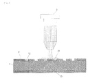
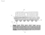
- FIGs. 1 to 5 are drawings schematically illustrating a method of manufacturing a semiconductor device of the present invention.
- the method of manufacturing a semiconductor device of the present invention will be explained below.
- a substrate 1 (circuit substrate) is prepared.
- the substrate 1 has an interconnect pattern 11 formed on one surface thereof (on the top side in FIG. 1 ), and electrode pad portions 12 are arranged.
- an electro-conductive material layer 13 is provided so as to allow therein formation of circuits in the later process.
- the coefficient of thermal expansion of the substrate 1 in the thickness-wise direction in the range from 25°C or above, up to the glass transition temperature (Tg) or below, is not specifically limited, it is preferably 20 ppm/°C or smaller, and particularly preferably 5 to 18 ppm/°C (expression of numerical range using "to", hereinafter, is defined to include the upper and lower limit values, unless otherwise specifically noted).
- Possible methods for obtaining such substrate 1 may be exemplified by a method of mixing a large amount of inorganic filler into a resin composition which composes the substrate 1, a method of using a material having a large elastic modulus for composing the substrate 1, and so forth.
- a pasty thermosetting resin composition 21 having a flux activity is coated, so as to cover the electrode pad portions 12 on the substrate 1 ( FIG. 2 , FIG. 3 ). While methods of coating are not specifically limited, a syringe 2 may be used as illustrated in FIG. 2 . While amount of coating of the pasty thermosetting resin composition 21 having a flux activity is not specifically limited, it may be good enough if at least the electrode pad portions 12 (sites of bonding) are covered typically as illustrated in FIG. 3 .
- the pasty thermosetting resin composition 21 having a flux activity may be exemplified by a resin composition containing a thermosetting resin and a flux activating agent.
- thermosetting resins such as an epoxy resin, a cyanate resin, a bismaleimide resin, an urethane resin, a polybutadiene resin, a silicone resin, a phenol resin, an urea resin, a melamine resin, an unsaturated polyester resin, an alkyd resin and so forth, may be adoptable.
- the epoxy resin is more preferable. Since the thermosetting resin herein is used for the purpose of encapsulating the semiconductor chip, those containing less amount of impurities, in particular ionic impurities, are preferable.
- the epoxy resin include bisphenol-type epoxy resins such as a bisphenol A-type epoxy resin, a bisphenol F-type epoxy resin, a bisphenol AD-type epoxy resin, and a bisphenol E-type epoxy resin; novolac-type epoxy resins such as a phenol novolac-type epoxy resin, and a cresol novolac-type epoxy resin; aromatic glycidyl amine-type epoxy resins such as a N,N-diglycidyl aniline, a N,N-diglycidyl toluidine, a diamino diphenylmethane-type glycidylamine, and an aminophenol-type glycidylamine; a hydroquinone-type epoxy resin; biphenyl-type epoxy resins such as a biphenylaralkyl-type epoxy resin; a stilbene-type epoxy resin; a triphenolmethane-type epoxy resin; a triphenol propane-type epoxy resin; an alkyl-modified triphenolmethane-
- thermosetting resin epoxy resin
- content of the thermosetting resin is not specifically limited, it may preferably be 5 to 70% by weight, and particularly preferably 10 to 50% by weight, of the whole portion of the pasty thermosetting resin composition 21.
- the pasty thermosetting resin composition 21 will be excellent particularly in thermal and mechanical characteristics including glass transition temperature, elastic modulus, and so forth.
- the flux activating agent refers to as a substance which exhibits an action of reducing oxide film on metal surface, to thereby expose the metal surface (flux action).
- the flux activating agent may be exemplified by phenolic compounds, acid or acid anhydride compounds, amine compounds, amide compounds, imidazoles, and activated rosin.
- the phenolic compounds may be exemplified by tetramethyl bisphenol A, catechol, resorcine, hydroquinone, xylenol, bisphenol.
- A bisphenol F, bisphenol AP, bisphenol S, bisphenol Z, dimethyl bisphenol A, dimethyl bisphenol F, tetramethyl bisphenol A, tetrame-thyl bisphenol F, biphenol, tetramethyl biphenol, dihydroxyphenyl ether, dihydroxybenzophenone, o -hydroxyphenol, m -hydroxyphenol, p -hydroxyphenol, polyphenols such as a phenol novolac resin and an orthocresol novolac resin, trisphenols such as a trihydroxy phenylmethane, and phenols having a naphthalene skeleton.
- the acid or acid anhydride compounds may be exemplified by formic acid, acetic acid, propionic acid, butyric acid, valeric acid, caproic acid, enanthic acid, caprylic acid, pelargonic acid, capric acid, lauric acid, myristic acid, palmitic acid, margaric acid, stearic acid, oleic acid, linoleic acid, linolenic acid, arachidonic acid, docosahexaenoic acid, eicosapentaenoic acid, oxalic acid, malonic acid, succinic acid, benzoic acid, phthalic acid, isophthalic acid, terephthalic acid, salicylic acid, gallic acid, mellitic acid, cinnamic acid, pyruvic acid, lactic acid, malic acid, citric acid, fumaric acid, maleic acid, aconitic acid, glutaric acid, adipic acid, pi
- compounds having both of a phenolic hydroxyl group and a carboxyl group may be adoptable.
- Specific examples include 2,3-dihydroxybenzoic acid, 2,4-dihydroxybenzoic acid, 2,5-dihydroxybenzoic acid, 2,6-dihydroxybenzoic acid, 3,4-dihydroxybenzoic acid, gallic acid, 1,4-dihydroxy-2-naphthoic acid, 3,5-dihydroxy-2-naphthoic acid, 3,7-dihydroxy-2-naphthoic acid, phenolphthalein, and diphenolic acid.
- the amine compounds may be exemplified by ethylenediamine, 1,3-diaminopropane, 1,4-diaminobutane, diethylenetriamine, triethylenetetramine, tetraethylenepentamine, pentaethylenehexamine, dipropylendiamine, diethylaminopropylamine, tri(methylamino)hexane, dimethylaminopropylamine, diethylaminopropylamine, methyliminobis(propylamine), hexamethylenediamine, diaminodiphenylmethane, diaminodiphenylsulfone, isophoronediamine, menthenediamine, isophoronediamine, bis(4-amino-3-methyldicyclohexyl)methane, diaminodicyclohexyl methane, N-aminoethylpiperadine, 3,9-bis(3-aminopropyl)-2
- the amide compounds may be exemplified by dicyanediamide, and polyamide resin synthesized by dimer of linolenic acid and ethylenediamine.
- the imidazoles may be exemplified, by 2-methylimidazole, 2-ethyl-4-methylimidazole, 2-undecylimidazole, 2-heptadecylimidazole, 2-phenyl-4,5-dihydroxy methylimidazole, 2-phenylimidazole, 2-ethylimidazole, and 2-ethyl-4-methylimidazole.
- These compounds may be used not only as a flux activating agent, and those crosslinkable with epoxy resin may be used also as a curing agent.
- content of the flux activating agent is not specifically limited, it is preferably 0.1 to 50% by weight, and in particular 1 to 40% by weight, of the whole portion of the pasty thermosetting resin composition 21.
- the flux activating agent can exhibit an excellent flux activity.
- the pasty thermosetting resin composition 21 can be ensured with excellent thermal and mechanical characteristics such as glass transition temperature and elastic modulus, and also with an excellent curing property.
- thermosetting resin such as epoxy resin
- curing agent having a flux activity those compounds having redox activity, contributive to curing reaction with thermosetting resin such as epoxy resin, and can be incorporated into the cross-linkage structure (curing agent having a flux activity) are preferable. With these compounds, cleaning of flux is no longer necessary, and thereby the pasty thermosetting resin composition 21 may be improved in the long-term reliability.
- the curing agent having a flux activity may be exemplified by phenolic compounds, acid anhydrides, imidazoles, and compounds having both of a phenolic hydroxyl group and a carboxyl group.
- the pasty thermosetting resin composition 21 having a flux activity may contain additives such as a curing agent, a filler and a coupling agent, besides the above-described thermosetting resin and the flux activating agent.
- the filler may be exemplified by inorganic fillers which include silicates such as talc, calcined clay, uncalcined clay, mica and glass; oxides such as titanium oxide, alumina, and silica powders such as fused silica (fused spherical silica, fused crushed silica), synthetic silica and crystalline silica; carbonates such as calcium carbonate, magnesium carbonate and hydrotalcite; hydroxides such as aluminum hydroxide, magnesium hydroxide and calcium hydroxide; sulfates or sulfites such as barium sulfate, calcium sulfate and calcium sulfate; borates such as zinc borate, barium metaborate, aluminum borate, calcium borate and sodium borate; and ni
- organic fillers may be adoptable.
- fused silica, crystalline silica and synthetic silica are preferable, in view of their possibilities of improving reliabilities such as heat resistance, moisture resistance and strength of liquid encapsulation resin composition.
- geometry of the filler is not specifically limited, spherical geometry is preferable from the viewpoint of viscosity and fluidization characteristics.
- content of the filler is not specifically limited, it is preferably 20 to 90% by weight, and in particular 30 to 85% by weight, of the whole portion of the pasty thermosetting resin composition 21.
- the content smaller than the above-described lower limit value may reduce an effect of improving reliabilities such as lowering the coefficient of linear expansion or lowering water absorption, whereas the content larger than the above-described upper limit value may increase viscosity of the thermosetting resin composition, and may consequently degrade the work efficiency and bump bonding performance.
- the coupling agent may be exemplified by vinyl trichlorosilane, vinyl trimethoxysilane, vinyl triethoxysilane, vinyl tri( ⁇ -methoxyethoxy)silane, ( ⁇ -(3,4-epoxycyclohexyl)ethyl trimethoxysilane, ⁇ -acryloxypropylmethyl dimethoxysilane, ⁇ -acryloxypropyl trimethoxysilane, ⁇ -acryloxypropylmethyl diethoxysilane, ⁇ -acryloxypropyl triethoxysilane, ⁇ -methacryloxypropylmethyl dimethoxysilane, ⁇ -methacryloxypropyl trimethoxysilane, ⁇ -methacryloxypropylmethyl diethoxysilane, ⁇ -methacryloxypropyl triethoxysilane, ⁇ -glycidoxypropyl trimethoxysilane, ⁇ -glycidoxypropyl trimeth
- content of the coupling agent is not specifically limited, it is preferably 0.1 to 20% by weight, and in particular 0.3 to 10% by weight, of the whole portion of the pasty thermosetting resin composition 21.
- the content smaller than the above-described lower limit value may degrade the adhesiveness or fluidity, whereas the content exceeding the above-described upper limit value may increase formation of volatile-induced voids.
- a semiconductor chip 3 is mounted on the substrate 1 using a flip-chip bonder 32.
- the semiconductor chip 3 is mounted while aligning solder bumps 31 (first electro-conductive portion) thereof with the electrode pad portions 12 (second electro-conductive portion) of the substrate 1 so as to bring them into contact ( FIG. 4 ).
- the solder bumps 31 are melted and electrically bonded to the electrode pad portions 12. Since the pasty thermosetting resin composition 21 herein has a flux activity, the solder-assisted bonding may proceed while removing the oxide film on the surface of the solder bumps 31 ( FIG. 5 ).
- the substrate 1 and the semiconductor chip 3 are electrically bonded, so that the solder bumps 31 and the electrode pad portions 12 are bonded by solder, while being covered with the pasty thermosetting resin composition 21.
- conditions of bonding are not specifically limited, it may be preferable to set temperature of the flip-chip bonder 32 higher by 10°C to 100°C than the melting point of the solder material used for the solder bumps 31, and to heat the solder bumps 31 for 1 to 30 seconds.
- the heating is more preferably effected only from the semiconductor chip 3 side.
- the first electro-conductive portion and the second electro-conductive portion are not limited to the solder bumps 31 and the electrode pad portions 12, respectively, and it may be good enough that at least either one represents the solder bumps, or alternatively, the both may represent the solder bumps.
- the pasty thermosetting resin composition 21 is then heated and cured. In this way, a gap between the solder bumps 31 and the electrode pad portions 12 may be filled up, and thereby reliability of bonding may be improved. While a means of heating and curing of the pasty thermosetting resin composition 21 is not specifically limited, an oven may typically be used. While conditions of heating depend on the thermosetting resin to be used, and are therefore not specifically limited, the heating may preferably be conducted at 100 to 200°C for 30 to 180 minutes, and particularly preferably at 120 to 170°C for 60 to 150 minutes. The temperature of heating is set not lower than the glass transition temperature of a cured product of the pasty thermosetting resin composition 21.
- the glass transition temperature of a cured product of the pasty thermosetting resin composition 21 having a flux activity, after the curing, is not specifically limited, it may preferably be 20°C to 300°C, and in particular 50°C to 150°C.
- the glass transition temperature By adjusting the glass transition temperature to the above-described lower limit value or higher, the bumps may more effectively be protected.
- a fillet composed of the pasty thermosetting resin composition 21 having a flux activity, formed after bonding of the substrate 1 and the semiconductor chip 3, may effectively be prevented from cracking.
- average linear coefficient of expansion ( ⁇ 1) in the range from 25°C or above up to the glass transition temperature or below, of the cured product of the pasty thermosetting resin composition 21 having a flux activity after the curing process is not specifically limited, it is preferably 5 ppm/°C to 60 ppm/°C, and in particular 15 ppm/°C to 40 ppm/°C.
- the average linear coefficient of expansion of the cured product of the pasty thermosetting resin composition 21 having a flux activity in the range not higher than the glass transition temperature, may be brought closer to the linear coefficient of expansion of the bumps (solder bumps 31). Accordingly, the bumps may effectively be prevented from cracking.
- the glass transition temperature and the linear coefficient of expansion of the pasty thermosetting resin composition 21 having a flux activity, after the curing process, may be measured according to a method descried below.
- the pasty thermosetting resin composition 21 having a flux activity is allowed to cure at 150°C for 3 hours, to thereby manufacture a 4 mm ⁇ 4 mm ⁇ 10 mm sample.
- the glass transition temperature, and the average linear coefficient of expansion in the range not higher than the glass transition temperature are calculated under a compressive load of 10 g, at a rate of temperature elevation of 10°C/min., over the range of measurement temperature from -100°C to 300°C.
- thermosetting resin composition is cooled at a cooling rate of 10 to 50 °C/h.
- a means of cooling adopted herein is such as succeedingly using the same oven having been used in the curing process, and setting conditions of cooling in the oven.
- the cooling rate may be constant or variable.
- the cooping rate may be calculated typically by dividing difference of temperature, which is obtained by subtracting temperature after the end of cooling process from temperature of atmosphere immediately after the curing process, by the cooling time.
- the temperature herein means, for example, temperature of the atmosphere in the oven.
- the semiconductor device has been obtained by carrying out soldering in a reflow oven, and then by curing a thermosetting resin, placed between a semiconductor chip and a wiring board, under heating at 120°C, without carrying out the cooling process.
- the semiconductor device has been taken out immediately after the curing, and exposed to room temperature.
- the semiconductor device is therefore abruptly cooled, at a cooling rate of at least 100°C/h or above.
- the thermosetting resin which is a viscoelastic product, then causes thermal distribution over the deep inner portion towards the surficial portion, and thereby produces residual stress.
- the constituent materials cause heat shrinkage due to abrupt cooling, and consequently a large stress produces due to large difference in the linear coefficients of expansion of the individual constituent materials.
- the process of manufacturing a semiconductor device of related art has inevitably resulted in warpage, due to abrupt cooling.
- the cooling process is adopted as described in the above.
- the cooling at a cooling rate of 10 to 50°C/h carried out in succession to the curing process, may moderate the mode of thermal shrinkage, and may further moderate the stress ascribable to difference in the linear coefficients of expansion of the constituent materials. Accordingly, the present invention may successfully moderate the stress in the process of cooling, to thereby reduce the warpage.
- the lower limit value of the cooling rate (first cooling rate) is preferably 15 °C/h or above, and more preferably 20°C/h or above.
- the upper limit value of the cooling rate (first cooling rate) is preferably 40°C/h or below, and more preferably 30°C/h or below.
- control range temperature range over which the cooling rate is controlled
- control range may be set to Tc [°C] or below, and (Tc-90) [°C] or above, assuming that the curing temperature of the pasty thermosetting resin composition 21 in the curing process as Tc [°C].
- the cooling is preferably performed at the above-described first cooling rate over the above-described temperature range.
- the control range of the first cooling rate may more specifically set to 150 to 60 [°C] while assuming the curing temperature (Tc) as 150 [°C], and more preferably 150 to 80 [°C].
- the cooling is preferably performed at the above-described first cooling rate over the above-described temperature range.
- the control range may be set to Tc [°C] or below, and (glass transition temperature of a cured product of the pasty thermosetting resin composition 21, minus 20) [°C] or above, and more specifically to 150 to (glass transition temperature (Tg) of a cured product of the pasty thermosetting resin composition 21, minus 20) [°C].
- the cooling is preferably performed at the above-described first cooling rate over the above-described temperature range.
- the control range set to the above-described range is particularly excellent in view of suppressing the warpage.
- the cooling rate out of the above-described control range may be defined as a second cooling rate. While the second cooling rate out of the above-described control range (in particular in the temperature range typically below (Tc-90) [°C]) is not specifically limited, it is preferably set to 60 to 120°C/h, and particularly preferably to 40 to 100°C/h. By the setting, an effect of moderating the stress and a good productivity may be achieved in a well-balanced manner.
- the above-described processes are followed by a process of forming solder bumps used for connection with a mother board, a process of mounting components and so forth, and thereby the semiconductor device may be obtained.
- the semiconductor device obtained in this way can protect the semiconductor chip, through protection of the bumps and suppression of the warpage.
- phenolphthalein Tokyo Chemical Industry Co., Ltd. (m.p.235°C)
- the above-described pasty thermosetting resin composition was coated on a circuit substrate having a circuit pattern formed thereon (with a core material made of ELC-4785GS from Sumitomo Bakelite Co., Ltd., having coefficients of thermal expansion (below Tg) of 11 ppm in the XY-direction, and 16 ppm in the Z-direction), and a semiconductor chip (15 mm long, 15 mm wide, and 0.725 mm thick), having solder bumps formed thereon, was mounted using a flip-chip bonder under heating at 260°C for 10 seconds. The pasty thermosetting resin composition was then cured under heating in a oven at 150°C for 120 minutes.
- the cooling was then performed at a cooling rate of 25°C/h over the control range from 150 down to 60°C, by setting condition of the oven relevant to the cooling rate, followed by cooling at a rate of approximately 60°C/h down to 30°C or around, to thereby obtain the semiconductor device.
- the temperature herein means temperature of the atmosphere in the oven.
- the processes of manufacturing a semiconductor device were conducted similarly as described in Example 1, except that the cooling rate was set as described below.
- the cooling was conducted over the range from 150 down to 60°C, at a cooling rate of 15°C/h.
- Example 2 The processes of manufacturing a semiconductor device were conducted similarly as described in Example 1, except that the range of cooling was set as described below.
- the cooling was conducted at the cooling rate same as that in Example 1 over the range from 150 down to 80°C, and at a cooling rate of 1°C/min over the range from not higher than 80°C down to 30°C.
- the processes of manufacturing a semiconductor device were conducted similarly as described in Example 1, except that the substrate described below was used.
- the substrate the one having a core composed of BT (CCL-HL832HS from Mitsubishi Gas Chemical Company, Inc., having coefficients of thermal expansion (Tg or below) of 15 ppm in the XY-direction, and 55 ppm in the Z-direction) was used.
- the process of manufacturing a semiconductor device was conducted similarly as described in Example 1, except that the cooling rate was set to as described below.
- the cooling was conducted over the range from 150 down to 60°C, at a cooling rate of 5°C/h.
- the pasty thermosetting resin composition described below was injected to a substrate having a semiconductor chip preliminarily mounted thereon, to thereby obtain a semiconductor package.
- 2-phenyl-4-methylimidazole from Shikoku Chemicals Corporation
- the semiconductor device was kept in the oven while keeping the curing temperature, and then taken out to immediately expose it to room temperature, and warpage of the semiconductor device was evaluated. Since the curing temperature herein was 150°C, the room temperature was 25°C, and the cooling time was 30 minutes or around, the semiconductor device was supposed to be cooled at a cooling rate of approximately 250°C/h or above. By the evaluation based on visual observation, the semiconductor device was found to cause warpage.
- thermosetting resin compositions obtained in Examples were cured at 150°C for 3 hours, to thereby manufacture samples having a size of 4 mm ⁇ 4 mm ⁇ 10 mm.
- Glass transition temperature, and average linear coefficient of expansion in the temperature range not higher than the glass transition temperature were calculated, using a TMA apparatus (from SII), under a compressive load of 10 g, at a rate of temperature elevation of 10°C/min., over the range of measurement temperature from -100°C to 300°C.
- Examples 1 to 6 were found to show only small warpage in both stages of as-manufactured and as-tested for reflow resistance. Examples 1 to 6 were also found to be excellent in the reliability. This suggested that the solder bumps were protected. Examples 1 to 6 were also found to be excellent in the work efficiency.
Landscapes
- Chemical & Material Sciences (AREA)
- Life Sciences & Earth Sciences (AREA)
- Engineering & Computer Science (AREA)
- Materials Engineering (AREA)
- Wood Science & Technology (AREA)
- Organic Chemistry (AREA)
- Wire Bonding (AREA)
- Structures Or Materials For Encapsulating Or Coating Semiconductor Devices Or Solid State Devices (AREA)
Abstract
Description
- The present invention relates to a method of manufacturing a semiconductor device, and a semiconductor device.
- In recent years, semiconductor packages have widely been diversified in association with downsizing, thinning and advancement in performance. In particular, methods of surface mounting of semiconductor chips with the aid of bumps such as solder bumps, aimed at increasing transmission speed of electric signals, are diversified. As this sort of method of mounting, methods of vertically mounting the semiconductor chips using metal bumps have been investigated, in view of further accelerating transmission of electric signals.
On the other hand, interconnect design of the semiconductor chips has increasingly been shrunk to make the pitches narrower, so that structure of the semiconductor chips has consequently been complicated in order to keep necessary levels of performances, and the semiconductor chips per se have been becoming more brittle.
In addition, referring to recent environmental awareness, metals per se adoptable to the bumps have been becoming lead-free, making it difficult to protect the bumps. - For this reason, requirements for characteristics to be owned have been becoming severer also for encapsulation materials (underfill material) used for this sort of bump bonding, so that it is now essential to achieve bump protection and chip protection at the same time. The underfill material preferably has a large elastic modulus from the viewpoint of bump protection, whereas preferably has a small elastic modulus from the viewpoint of protecting the chips (reducing warpage of the chips). In short, the underfill material is required to have contradictory characteristics with respect to the bump protection and chip protection. To solve this problem, investigations have been made on balancing the physical characteristics of the underfill material (see
Patent Documents - However, typically due to complication of the semiconductor packages and dimensional restriction, only a limited degree of upgrading of performances has been achievable simply by balancing the physical characteristics of the under fill material, and the situation has inevitably demanded re-designing of the structure per se, or has even put off the lead-free roadmap in order to clear a required level of reliability.
-
- [Patent Document 1] Japnaese Laid-Open Patent Publication No. H07-335791
- [Patent Document 2] Japnaese Laid-Open Patent Publication No. H10-204259
- The present invention is to provide a method of manufacturing a semiconductor device, capable of protecting the bumps, and of also protecting the semiconductor chip by reducing warpage.
- The object described in the above may be achieved by the present invention described in (1) to (18) below.
- (1) A method of manufacturing a semiconductor device substrate which includes:
- a coating process in which a pasty thermosetting resin composition having a flux activity is coated on at least either one of a substrate and a semiconductor chip;
- a bonding process in which the substrate and the semiconductor chip are electrically bonded while placing the pasty thermosetting resin composition in between;
- a curing process in which the pasty thermosetting resin composition is cured under heating; and
- a cooling process, succeeding to the curing process, in which cooling is performed at a cooling rate between 10 [°C/hour] or above, and 50 [°C/hour] or below.
- (2) The method of manufacturing a Semiconductor device as described in (1),
wherein, assuming that the curing temperature of the pasty thermosetting resin composition in the curing process as Tc [°C], in the cooling process, said step of cooling is performed at said cooling rate between Tc [°C] or below and down to (Tc-90) [°C] or above. - (3) The method of manufacturing a semiconductor device as described in (2),
wherein, assuming that the curing temperature (Tc) as 150 [°C], in the cooling process , said step of cooling is performed at said cooling rate between 150 [°C] or above and 60 [°C] or below. - (4) The method of manufacturing a semiconductor device as described in (2),
wherein said step of cooling is performed at said cooling rate between 60 [°C/hour] or above, and 120 [°C/hour] or below, in the temperature range lower than (Tc-90) [°C]. - (5) The method of manufacturing a semiconductor device as described in (1),
wherein linear coefficient of expansion (α1) of the substrate in the thickness-wise direction thereof, in the range from 25°C or above, up to glass transition temperature (Tg) or below, is 20 ppm/°C or smaller. - (6) The method of manufacturing a semiconductor device as described in (1),
wherein linear coefficient of expansion (α1) of the substrate in the thickness-wise direction thereof, in the range from 25°C or above, up to glass transition temperature (Tg) or below, is 5 ppm/°C or larger. - (7) The method of manufacturing a semiconductor device as described in (1),
wherein the glass transition temperature of a cured product of the pasty thermosetting resin composition after the curing process is 50°C or above and 150°C or below. - (8) The method of manufacturing a semiconductor device as described in (2),
wherein the glass transition temperature of a cured product of the pasty thermosetting resin composition after the curing process is 50°C or above and 150°C or below. - (9) The method of manufacturing a semiconductor device as described in (8),
wherein, in the cooling process, said step of cooling is performed at said cooling rate between Tc [°C] or below and (the glass transition temperature of a cured product of the pasty thermosetting resin composition minus 20) [°C] or above. - (10) The method of manufacturing a semiconductor device as described in (1),
wherein linear coefficient of expansion of a cured product of the pasty thermosetting resin composition after the curing process, over the range from 25°C or above, up to the glass transition temperature (Tg) or below, is 5 ppm/°C or larger, and 60 ppm/°C or smaller. - (11) The method of manufacturing a semiconductor device as described in (1),
wherein, in the cooling process, the cooling rate is 25 [°C/hour] or below. - (12) The method of manufacturing a semiconductor device as described in (1),
using the substrate having a first electro-conductive portion, and the semiconductor chip having a second electro-conductive portion,
in the bonding process, the substrate and the semiconductor chip are electrically bonded, while being covered with the pasty thermosetting resin composition, so as to connect the first electro-conductive portion and the second electro-conductive portion with a solder. - (13) The method of manufacturing a semiconductor device as described in (12),
wherein at least either one of the first electro-conductive portion and the second electro-conductive portion is composed of solder bumps. - (14) The method of manufacturing a semiconductor device as described in (1),
wherein the pasty thermosetting resin composition contains a thermosetting resin and a flux activating agent. - (15) The method of manufacturing a semiconductor device as described in (14),
wherein content of the thermosetting resin is 5% by weight or more, and 70% by weight or less of the whole portion of the pasty thermosetting resin composition. - (16) The method of manufacturing a semiconductor device as described in (14),
wherein content of the flux activating agent is 0.1% by weight or more, and 50% by weight or less of the whole portion of the pasty thermosetting resin composition. - (17) The method of manufacturing a semiconductor device as described in (14),
wherein the flux activating agent has a carboxyl group and a phenolic hydroxyl group in the molecule thereof. - (18) A. semiconductor device obtained by the method of manufacturing a semiconductor device described in any one of (1) to (17).
- According to the present invention, there is provided a method of manufacturing a semiconductor device, capable of protecting the bumps, and of also protecting the semiconductor chip by reducing warpage.
- The above and other objects, features and advantages of the present invention will be more apparent from the following description of certain preferred embodiments taken in conjunction with the accompanying drawings.
-
FIG. 1 is a sectional view illustrating an exemplary method of manufacturing a semiconductor device. -
FIG. 2 is a sectional view illustrating an exemplary method of manufacturing a semiconductor device. -
FIG. 3 is a sectional view illustrating an exemplary method of manufacturing a semiconductor device. -
FIG. 4 is a sectional view illustrating an exemplary method of manufacturing a semiconductor device. -
FIG. 5 is a sectional view illustrating an exemplary method of manufacturing a semiconductor device. - The method of manufacturing a semiconductor device of the present invention will be detailed below.
The method of manufacturing a semiconductor device of the present invention has a coating process in which a pasty thermosetting resin composition having a flux activity is coated on at least either one of a substrate and a semiconductor chip; a bonding process in which the substrate and the semiconductor chip are electrically bonded while placing the pasty thermosetting resin composition in between; a curing process in which the pasty thermosetting resin composition is cured under heating; and a cooling process, succeeding to the curing process, in which cooling is performed at a cooling rate of 10 [°C/hour] or above, and 50 [°C/hour] or below (note that [°C/hour] may occasionally be expressed as [°C/h]). -
FIGs. 1 to 5 are drawings schematically illustrating a method of manufacturing a semiconductor device of the present invention.
The method of manufacturing a semiconductor device of the present invention will be explained below.
First, as illustrated inFIG. 1 , a substrate 1 (circuit substrate) is prepared. Thesubstrate 1 has aninterconnect pattern 11 formed on one surface thereof (on the top side inFIG. 1 ), andelectrode pad portions 12 are arranged. On the other surface of the substrate 1 (on the bottom side inFIG. 1 ), an electro-conductive material layer 13 is provided so as to allow therein formation of circuits in the later process. - While the coefficient of thermal expansion of the
substrate 1 in the thickness-wise direction, in the range from 25°C or above, up to the glass transition temperature (Tg) or below, is not specifically limited, it is preferably 20 ppm/°C or smaller, and particularly preferably 5 to 18 ppm/°C (expression of numerical range using "to", hereinafter, is defined to include the upper and lower limit values, unless otherwise specifically noted). By adjusting the coefficient in this range, stress possibly produced due to difference in the linear coefficients of expansion between the chip and the substrate may be suppressed, and thereby the warpage may more effectively be suppressed. - Possible methods for obtaining
such substrate 1 may be exemplified by a method of mixing a large amount of inorganic filler into a resin composition which composes thesubstrate 1, a method of using a material having a large elastic modulus for composing thesubstrate 1, and so forth. - Next, a pasty
thermosetting resin composition 21 having a flux activity is coated, so as to cover theelectrode pad portions 12 on the substrate 1 (FIG. 2 ,FIG. 3 ). While methods of coating are not specifically limited, asyringe 2 may be used as illustrated inFIG. 2 .
While amount of coating of the pastythermosetting resin composition 21 having a flux activity is not specifically limited, it may be good enough if at least the electrode pad portions 12 (sites of bonding) are covered typically as illustrated inFIG. 3 .
The pastythermosetting resin composition 21 having a flux activity may be exemplified by a resin composition containing a thermosetting resin and a flux activating agent. - As the thermosetting resign, any of publicly-known thermosetting resins, such as an epoxy resin, a cyanate resin, a bismaleimide resin, an urethane resin, a polybutadiene resin, a silicone resin, a phenol resin, an urea resin, a melamine resin, an unsaturated polyester resin, an alkyd resin and so forth, may be adoptable. The epoxy resin is more preferable. Since the thermosetting resin herein is used for the purpose of encapsulating the semiconductor chip, those containing less amount of impurities, in particular ionic impurities, are preferable.
- Specific examples of the epoxy resin include bisphenol-type epoxy resins such as a bisphenol A-type epoxy resin, a bisphenol F-type epoxy resin, a bisphenol AD-type epoxy resin, and a bisphenol E-type epoxy resin; novolac-type epoxy resins such as a phenol novolac-type epoxy resin, and a cresol novolac-type epoxy resin; aromatic glycidyl amine-type epoxy resins such as a N,N-diglycidyl aniline, a N,N-diglycidyl toluidine, a diamino diphenylmethane-type glycidylamine, and an aminophenol-type glycidylamine; a hydroquinone-type epoxy resin; biphenyl-type epoxy resins such as a biphenylaralkyl-type epoxy resin; a stilbene-type epoxy resin; a triphenolmethane-type epoxy resin; a triphenol propane-type epoxy resin; an alkyl-modified triphenolmethane-type epoxy resin; a triazine-core-containing epoxy resin; a dicyclopentadiene-modified phenolic epoxy resin; a naphthol-type epoxy resin; naphthalene-type epoxy resin; a phenolaralkyl-type epoxy resins having a phenylene and/or a biphenylene skeleton; epoxy resins such as aralkyl-type epoxy resins such as a naphthol aralkyl-type epoxy resin having a phenylene and/or a biphenylene skeleton; a vinylcyclohexene dioxide; a dicyclopentadiene oxide; aliphatic epoxy resins such as alicyclic epoxys such as an alicyclic diepoxy-adipate; and bromine-containing epoxy resins.
- While content of the thermosetting resin (epoxy resin) is not specifically limited, it may preferably be 5 to 70% by weight, and particularly preferably 10 to 50% by weight, of the whole portion of the pasty
thermosetting resin composition 21. By adjusting the content into the ranges described in the above, the pastythermosetting resin composition 21 will be excellent particularly in thermal and mechanical characteristics including glass transition temperature, elastic modulus, and so forth. - The flux activating agent refers to as a substance which exhibits an action of reducing oxide film on metal surface, to thereby expose the metal surface (flux action).
The flux activating agent may be exemplified by phenolic compounds, acid or acid anhydride compounds, amine compounds, amide compounds, imidazoles, and activated rosin.
The phenolic compounds may be exemplified by tetramethyl bisphenol A, catechol, resorcine, hydroquinone, xylenol, bisphenol. A, bisphenol F, bisphenol AP, bisphenol S, bisphenol Z, dimethyl bisphenol A, dimethyl bisphenol F, tetramethyl bisphenol A, tetrame-thyl bisphenol F, biphenol, tetramethyl biphenol, dihydroxyphenyl ether, dihydroxybenzophenone, o-hydroxyphenol, m-hydroxyphenol, p-hydroxyphenol, polyphenols such as a phenol novolac resin and an orthocresol novolac resin, trisphenols such as a trihydroxy phenylmethane, and phenols having a naphthalene skeleton. - The acid or acid anhydride compounds may be exemplified by formic acid, acetic acid, propionic acid, butyric acid, valeric acid, caproic acid, enanthic acid, caprylic acid, pelargonic acid, capric acid, lauric acid, myristic acid, palmitic acid, margaric acid, stearic acid, oleic acid, linoleic acid, linolenic acid, arachidonic acid, docosahexaenoic acid, eicosapentaenoic acid, oxalic acid, malonic acid, succinic acid, benzoic acid, phthalic acid, isophthalic acid, terephthalic acid, salicylic acid, gallic acid, mellitic acid, cinnamic acid, pyruvic acid, lactic acid, malic acid, citric acid, fumaric acid, maleic acid, aconitic acid, glutaric acid, adipic acid, pimelic acid, suberic acid, azelaic acid, sebacic acid, amino acid, nitrocarboxylic acid, abietic acid, phthalic anhydride, trimellitic anhydride, pyromellitic anhydride, maleic anhydride, benzophenone tetracarboxylic anhydride, ethylene glycol bistrimellitate, het anhydride, tetrabromophthalic anhydride, tetrahydrophthalic anhydride, methyl tetrahydrophthalic anhydride, methyl nadic anhydride, hexahydrophthalic anhydride, methyl hexahydrophthalic anhydride, dodecyl succinic anhhydride, polyadipic anhydride, polyazelaic anhydride, polysebacic anhydride, poly(ethyl octadecanedioic)anhydride, poly(phenylhexadecanedioic)anhydride, methylhimic anhydride, trialkyl tetrahydrophthalic anhydride, and methyl cyclohexene dicarboxylic anhydride.
- Also compounds having both of a phenolic hydroxyl group and a carboxyl group may be adoptable. Specific examples include 2,3-dihydroxybenzoic acid, 2,4-dihydroxybenzoic acid, 2,5-dihydroxybenzoic acid, 2,6-dihydroxybenzoic acid, 3,4-dihydroxybenzoic acid, gallic acid, 1,4-dihydroxy-2-naphthoic acid, 3,5-dihydroxy-2-naphthoic acid, 3,7-dihydroxy-2-naphthoic acid, phenolphthalein, and diphenolic acid.
- The amine compounds may be exemplified by ethylenediamine, 1,3-diaminopropane, 1,4-diaminobutane, diethylenetriamine, triethylenetetramine, tetraethylenepentamine, pentaethylenehexamine, dipropylendiamine, diethylaminopropylamine, tri(methylamino)hexane, dimethylaminopropylamine, diethylaminopropylamine, methyliminobis(propylamine), hexamethylenediamine, diaminodiphenylmethane, diaminodiphenylsulfone, isophoronediamine, menthenediamine, isophoronediamine, bis(4-amino-3-methyldicyclohexyl)methane, diaminodicyclohexyl methane, N-aminoethylpiperadine, 3,9-bis(3-aminopropyl)-2,4,8,10-tetraoxaspiro(5,5)undecane, 2,5-dimethyl hexamethylenediamine, trimethyl hexamethylenediamine, iminobis(propylamine), bis(hexamethyle)triamine, m-xylenediamine, meta-phenylenediamine, diaminodiethylphenyl methane, and polyetherdiamine.
- The amide compounds may be exemplified by dicyanediamide, and polyamide resin synthesized by dimer of linolenic acid and ethylenediamine.
The imidazoles may be exemplified, by 2-methylimidazole, 2-ethyl-4-methylimidazole, 2-undecylimidazole, 2-heptadecylimidazole, 2-phenyl-4,5-dihydroxy methylimidazole, 2-phenylimidazole, 2-ethylimidazole, and 2-ethyl-4-methylimidazole.
These compounds may be used not only as a flux activating agent, and those crosslinkable with epoxy resin may be used also as a curing agent. - While content of the flux activating agent is not specifically limited, it is preferably 0.1 to 50% by weight, and in particular 1 to 40% by weight, of the whole portion of the pasty
thermosetting resin composition 21. By adjusting the content in the above-described ranges, the flux activating agent can exhibit an excellent flux activity. In particular for the case where the flux activating agent is used also as a curing agent, the pastythermosetting resin composition 21 can be ensured with excellent thermal and mechanical characteristics such as glass transition temperature and elastic modulus, and also with an excellent curing property. - Among these flux activating agent, those compounds having redox activity, contributive to curing reaction with thermosetting resin such as epoxy resin, and can be incorporated into the cross-linkage structure (curing agent having a flux activity) are preferable. With these compounds, cleaning of flux is no longer necessary, and thereby the pasty
thermosetting resin composition 21 may be improved in the long-term reliability.
The curing agent having a flux activity may be exemplified by phenolic compounds, acid anhydrides, imidazoles, and compounds having both of a phenolic hydroxyl group and a carboxyl group. - The pasty
thermosetting resin composition 21 having a flux activity may contain additives such as a curing agent, a filler and a coupling agent, besides the above-described thermosetting resin and the flux activating agent.
The filler may be exemplified by inorganic fillers which include silicates such as talc, calcined clay, uncalcined clay, mica and glass; oxides such as titanium oxide, alumina, and silica powders such as fused silica (fused spherical silica, fused crushed silica), synthetic silica and crystalline silica; carbonates such as calcium carbonate, magnesium carbonate and hydrotalcite; hydroxides such as aluminum hydroxide, magnesium hydroxide and calcium hydroxide; sulfates or sulfites such as barium sulfate, calcium sulfate and calcium sulfate; borates such as zinc borate, barium metaborate, aluminum borate, calcium borate and sodium borate; and nitrides such as aluminum nitride, boron nitride and silicon nitride. Also organic fillers may be adoptable. Among these, fused silica, crystalline silica and synthetic silica are preferable, in view of their possibilities of improving reliabilities such as heat resistance, moisture resistance and strength of liquid encapsulation resin composition. While geometry of the filler is not specifically limited, spherical geometry is preferable from the viewpoint of viscosity and fluidization characteristics. - While content of the filler is not specifically limited, it is preferably 20 to 90% by weight, and in particular 30 to 85% by weight, of the whole portion of the pasty
thermosetting resin composition 21. The content smaller than the above-described lower limit value may reduce an effect of improving reliabilities such as lowering the coefficient of linear expansion or lowering water absorption, whereas the content larger than the above-described upper limit value may increase viscosity of the thermosetting resin composition, and may consequently degrade the work efficiency and bump bonding performance. - The coupling agent may be exemplified by vinyl trichlorosilane, vinyl trimethoxysilane, vinyl triethoxysilane, vinyl tri(β-methoxyethoxy)silane, (β-(3,4-epoxycyclohexyl)ethyl trimethoxysilane, γ-acryloxypropylmethyl dimethoxysilane, γ-acryloxypropyl trimethoxysilane, γ-acryloxypropylmethyl diethoxysilane, γ-acryloxypropyl triethoxysilane, γ-methacryloxypropylmethyl dimethoxysilane, γ-methacryloxypropyl trimethoxysilane, γ-methacryloxypropylmethyl diethoxysilane, γ-methacryloxypropyl triethoxysilane, γ-glycidoxypropyl trimethoxysilane, γ-glycidoxypropyl trimethoxysilane, γ-glycidoxypropylmethyl diethoxysilane, γ-glycidoxypropyl triethoxysilane, p-styryl trimethoxysilane, N-(β-aminoethyl-γ-aminopropylmethyl)dimethoxysilane, N-(γ-aminoethyl-γ-aminopropyl)trimethoxysilane, N-(β-aminoethyl-γ-aminopropyl)triethoxysilane, γ-aminopropyl triethoxysilane, and γ-phenyl-γ-aminopropyl trimethoxysilane. These compounds may be used independently, or may be used in a form of mixture. Among these coupling agent, amine terminal-type silane coupling agents are preferable. By the selection, the fluidity and adhesiveness may be improved.
- While content of the coupling agent is not specifically limited, it is preferably 0.1 to 20% by weight, and in particular 0.3 to 10% by weight, of the whole portion of the pasty
thermosetting resin composition 21. The content smaller than the above-described lower limit value may degrade the adhesiveness or fluidity, whereas the content exceeding the above-described upper limit value may increase formation of volatile-induced voids. - Next, a
semiconductor chip 3 is mounted on thesubstrate 1 using a flip-chip bonder 32. In this process, thesemiconductor chip 3 is mounted while aligning solder bumps 31 (first electro-conductive portion) thereof with the electrode pad portions 12 (second electro-conductive portion) of thesubstrate 1 so as to bring them into contact (FIG. 4 ). In the process of mounting, the solder bumps 31 are melted and electrically bonded to theelectrode pad portions 12. Since the pastythermosetting resin composition 21 herein has a flux activity, the solder-assisted bonding may proceed while removing the oxide film on the surface of the solder bumps 31 (FIG. 5 ). In other words, in this process of bonding, thesubstrate 1 and thesemiconductor chip 3 are electrically bonded, so that the solder bumps 31 and theelectrode pad portions 12 are bonded by solder, while being covered with the pastythermosetting resin composition 21. - While conditions of bonding are not specifically limited, it may be preferable to set temperature of the flip-
chip bonder 32 higher by 10°C to 100°C than the melting point of the solder material used for the solder bumps 31, and to heat the solder bumps 31 for 1 to 30 seconds. In this process, the heating is more preferably effected only from thesemiconductor chip 3 side. By this way of heating, thermal stress otherwise possibly be applied to the substrate may be reduced, warpage of the semiconductor device otherwise possibly occurs due to difference in the linear coefficients of expansion between the substrate and the chip may be reduced, and also the volatile-induced voids ascribable to the substrate may be suppressed.
In this embodiment, the first electro-conductive portion and the second electro-conductive portion are not limited to the solder bumps 31 and theelectrode pad portions 12, respectively, and it may be good enough that at least either one represents the solder bumps, or alternatively, the both may represent the solder bumps. - The pasty
thermosetting resin composition 21 is then heated and cured. In this way, a gap between the solder bumps 31 and theelectrode pad portions 12 may be filled up, and thereby reliability of bonding may be improved. While a means of heating and curing of the pastythermosetting resin composition 21 is not specifically limited, an oven may typically be used.
While conditions of heating depend on the thermosetting resin to be used, and are therefore not specifically limited, the heating may preferably be conducted at 100 to 200°C for 30 to 180 minutes, and particularly preferably at 120 to 170°C for 60 to 150 minutes. The temperature of heating is set not lower than the glass transition temperature of a cured product of the pastythermosetting resin composition 21. - While the glass transition temperature of a cured product of the pasty
thermosetting resin composition 21 having a flux activity, after the curing, is not specifically limited, it may preferably be 20°C to 300°C, and in particular 50°C to 150°C. By adjusting the glass transition temperature to the above-described lower limit value or higher, the bumps may more effectively be protected. On the other hand, by adjusting the glass transition temperature to the above-described upper limit value or lower, a fillet composed of the pastythermosetting resin composition 21 having a flux activity, formed after bonding of thesubstrate 1 and thesemiconductor chip 3, may effectively be prevented from cracking. - While average linear coefficient of expansion (α1), in the range from 25°C or above up to the glass transition temperature or below, of the cured product of the pasty
thermosetting resin composition 21 having a flux activity after the curing process is not specifically limited, it is preferably 5 ppm/°C to 60 ppm/°C, and in particular 15 ppm/°C to 40 ppm/°C. By adjusting the glass transition temperature in the above-described ranges, the average linear coefficient of expansion of the cured product of the pastythermosetting resin composition 21 having a flux activity, in the range not higher than the glass transition temperature, may be brought closer to the linear coefficient of expansion of the bumps (solder bumps 31). Accordingly, the bumps may effectively be prevented from cracking. - The glass transition temperature and the linear coefficient of expansion of the pasty
thermosetting resin composition 21 having a flux activity, after the curing process, may be measured according to a method descried below.
The pastythermosetting resin composition 21 having a flux activity is allowed to cure at 150°C for 3 hours, to thereby manufacture a 4 mm×4 mm×10 mm sample. Next, using a TMA device (from SII), the glass transition temperature, and the average linear coefficient of expansion in the range not higher than the glass transition temperature, are calculated under a compressive load of 10 g, at a rate of temperature elevation of 10°C/min., over the range of measurement temperature from -100°C to 300°C. - Next, after the curing process, the thermosetting resin composition is cooled at a cooling rate of 10 to 50 °C/h. A means of cooling adopted herein is such as succeedingly using the same oven having been used in the curing process, and setting conditions of cooling in the oven. The cooling rate may be constant or variable. The cooping rate may be calculated typically by dividing difference of temperature, which is obtained by subtracting temperature after the end of cooling process from temperature of atmosphere immediately after the curing process, by the cooling time. The temperature herein means, for example, temperature of the atmosphere in the oven.
By cooling the thermosetting resin composition at a cooling rate of 10 to 50°C/h (first cooling rate) as described in the above, in particular at a constant cooling rate, the stress in the process of cooling may be moderated, and thereby the warpage may be reduced. - In one example of the process of manufacturing a semiconductor device of related art, as described in
Patent Document 2, the semiconductor device has been obtained by carrying out soldering in a reflow oven, and then by curing a thermosetting resin, placed between a semiconductor chip and a wiring board, under heating at 120°C, without carrying out the cooling process. As described in the above, from the viewpoint of productivity, the semiconductor device has been taken out immediately after the curing, and exposed to room temperature. The semiconductor device is therefore abruptly cooled, at a cooling rate of at least 100°C/h or above. The thermosetting resin, which is a viscoelastic product, then causes thermal distribution over the deep inner portion towards the surficial portion, and thereby produces residual stress. In other words, the constituent materials cause heat shrinkage due to abrupt cooling, and consequently a large stress produces due to large difference in the linear coefficients of expansion of the individual constituent materials. As described in the above, the process of manufacturing a semiconductor device of related art has inevitably resulted in warpage, due to abrupt cooling. - In contrast, in the process of manufacturing a semiconductor device of the present invention, the cooling process is adopted as described in the above. The cooling at a cooling rate of 10 to 50°C/h, carried out in succession to the curing process, may moderate the mode of thermal shrinkage, and may further moderate the stress ascribable to difference in the linear coefficients of expansion of the constituent materials. Accordingly, the present invention may successfully moderate the stress in the process of cooling, to thereby reduce the warpage.
- The lower limit value of the cooling rate (first cooling rate) is preferably 15 °C/h or above, and more preferably 20°C/h or above. On the other hand, the upper limit value of the cooling rate (first cooling rate) is preferably 40°C/h or below, and more preferably 30°C/h or below. By adjusting the cooling rate to the above-described lower limit value or above, the warpage may be suppressed in a more improved manner. On the other hand, by adjusting the cooling rate to the above-described upper limit value or below, the warpage may be suppressed in a more improved manner.
- While, in the cooling process, temperature range over which the cooling rate is controlled (occasionally referred to as control range, hereinafter) is not specifically limited, it may be set to Tc [°C] or below, and (Tc-90) [°C] or above, assuming that the curing temperature of the pasty
thermosetting resin composition 21 in the curing process as Tc [°C]. The cooling is preferably performed at the above-described first cooling rate over the above-described temperature range. By this way of cooling, the generated stress may be more distinctively reduced in the control range, and by controlling the temperature range, the warpage may be suppressed in a more improved manner. - The control range of the first cooling rate may more specifically set to 150 to 60 [°C] while assuming the curing temperature (Tc) as 150 [°C], and more preferably 150 to 80 [°C]. The cooling is preferably performed at the above-described first cooling rate over the above-described temperature range. In particular, the control range may be set to Tc [°C] or below, and (glass transition temperature of a cured product of the pasty
thermosetting resin composition 21, minus 20) [°C] or above, and more specifically to 150 to (glass transition temperature (Tg) of a cured product of the pastythermosetting resin composition 21, minus 20) [°C]. The cooling is preferably performed at the above-described first cooling rate over the above-described temperature range. The control range set to the above-described range is particularly excellent in view of suppressing the warpage. - The cooling rate out of the above-described control range may be defined as a second cooling rate. While the second cooling rate out of the above-described control range (in particular in the temperature range typically below (Tc-90) [°C]) is not specifically limited, it is preferably set to 60 to 120°C/h, and particularly preferably to 40 to 100°C/h. By the setting, an effect of moderating the stress and a good productivity may be achieved in a well-balanced manner.
- The above-described processes are followed by a process of forming solder bumps used for connection with a mother board, a process of mounting components and so forth, and thereby the semiconductor device may be obtained. The semiconductor device obtained in this way can protect the semiconductor chip, through protection of the bumps and suppression of the warpage.
- The present invention will be detailed below, referring to Examples and Comparative Examples, while ensuring that the present invention is not limited thereto.
- A pasty thermosetting resin composition was obtained by weighing 70.9% by weight of bisphenol F-type epoxy resin (from DIC Corpoartion, EXA-830LVP, epoxy equivalent weight=161) as the thermosetting resin, 21.3% by weight of phenol novolac (from Sumitomo Durez Co., Ltd., PR-51470, softening point=110°C) as the curing agent, 7.1% by weight of phenolphthalein (Tokyo Chemical Industry Co., Ltd. (m.p.235°C)) as the flux activating agent, and. 0.7% by weight of 2-phenyl -4-methylimidazole (from Shikoku Chemicals Corporation, 2P4MZ) as a curing accelerator, and by dispersing the mixture under kneading using a three-roll mill, followed by defoaming in vacuo.
- The above-described pasty thermosetting resin composition was coated on a circuit substrate having a circuit pattern formed thereon (with a core material made of ELC-4785GS from Sumitomo Bakelite Co., Ltd., having coefficients of thermal expansion (below Tg) of 11 ppm in the XY-direction, and 16 ppm in the Z-direction), and a semiconductor chip (15 mm long, 15 mm wide, and 0.725 mm thick), having solder bumps formed thereon, was mounted using a flip-chip bonder under heating at 260°C for 10 seconds. The pasty thermosetting resin composition was then cured under heating in a oven at 150°C for 120 minutes.
The cooling was then performed at a cooling rate of 25°C/h over the control range from 150 down to 60°C, by setting condition of the oven relevant to the cooling rate, followed by cooling at a rate of approximately 60°C/h down to 30°C or around, to thereby obtain the semiconductor device. Note that the temperature herein means temperature of the atmosphere in the oven. - The processes of manufacturing a semiconductor device were conducted similarly as described in Example 1, except that the cooling rate was set as described below.
The cooling was conducted over the range from 150 down to 60°C, at a cooling rate of 15°C/h. - The processes of manufacturing a semiconductor device were conducted similarly as described in Example 1, except that the range of cooling was set as described below.
The cooling was conducted at the cooling rate same as that in Example 1 over the range from 150 down to 80°C, and at a cooling rate of 1°C/min over the range from not higher than 80°C down to 30°C. - The processes of manufacturing a semiconductor device were conducted similarly as described in Example 1, except that the materials below were used as the pasty thermosetting resin composition.
A pasty thermosetting resin composition was obtained by weighing 76.3% by weight of bisphenol F-type epoxy resin (EXA-830LVP from DIC Corporation, epoxy equivalent weight=161) as the thermosetting resin, 22.9% by weight of 2,5-dihydroxybenzoic acid (from Tokyo Chemical Industry Co., Ltd. (m.p.=200 to 205°C)) as the curing agent having a flux activity, and 0.8% by weight of 2-phenyl-4-methylimidazole (from Shikoku Chemicals Corporation) as the curing accelerator, and by dispersing the mixture under kneading using a three-roll mill, followed by defoaming in vacuo. - The processes of manufacturing a semiconductor device were conducted similarly as described in Example 1, except that the pasty thermosetting resin composition was coated not onto the substrate, instead onto the semiconductor chip.
- The processes of manufacturing a semiconductor device were conducted similarly as described in Example 1, except that the substrate described below was used.
As the substrate, the one having a core composed of BT (CCL-HL832HS from Mitsubishi Gas Chemical Company, Inc., having coefficients of thermal expansion (Tg or below) of 15 ppm in the XY-direction, and 55 ppm in the Z-direction) was used. - The process of manufacturing a semiconductor device was conducted similarly as described in Example 1, except that the cooling rate was set to as described below.
The cooling was conducted over the range from 150 down to 60°C, at a cooling rate of 5°C/h. - In the process of manufacturing a semiconductor device, the pasty thermosetting resin composition described below was injected to a substrate having a semiconductor chip preliminarily mounted thereon, to thereby obtain a semiconductor package.
The pasty thermosetting resin composition was obtained by weighing 79.4% by weight of bisphenol F-type epoxy resin (EXA-830LVP from DIC Corporation, epoxy equivalent weight=161) as the thermosetting resin, 19.8% by weight of phenol novolac as the curing agent, and 0.8% by weight of 2-phenyl-4-methylimidazole (from Shikoku Chemicals Corporation) as the curing accelerator, and by dispersing the mixture under kneading using a three-roll mill, followed by defoaming in vacuo. - In addition, after the curing process, the semiconductor device was kept in the oven while keeping the curing temperature, and then taken out to immediately expose it to room temperature, and warpage of the semiconductor device was evaluated. Since the curing temperature herein was 150°C, the room temperature was 25°C, and the cooling time was 30 minutes or around, the semiconductor device was supposed to be cooled at a cooling rate of approximately 250°C/h or above. By the evaluation based on visual observation, the semiconductor device was found to cause warpage.
- The semiconductor devices obtained in the individual Examples and Comparative Examples were evaluated with respect to the items below. The items of evaluation and the criteria are shown. Results are shown in Table 1.
- Warpage of the obtained semiconductor devices, and warpage of the semiconductor device after the reflow resistance test described later were evaluated. Explanations of the marks are as follow:
- A: the amount of warpage did not exceed 80 µm;
- B: the amount of warpage exceeded 80 µm, but did not exceed 100 µm;
- C: the amount of warpage exceeded 100 µm, but did not exceed 120 µm; and
- D: the amount of warpage exceeded 120 µm.
- Reliability of the semiconductor devices was evaluated based on separation property and bonding property of the semiconductor device, after being subjected to reflow resistance test conforming to
JEDEC level 3, under which SMT reflow was conducted (three times) at a peak temperature of 260°C. The evaluation was made under n=20. Explanations of the marks are as follow. -
- A: separation was not observed for all samples;
- B: incidence of separation was smaller than 5%;
- C: incidence of separation was 5% or larger, and smaller than 10%; and
- D: incidence of separation was 10% or larger.
-
- A: ratio of bonding was 100%;
- B: ratio of bonding was smaller than 100% (8/10 or larger), and 95% or larger (2/10 or smaller);
- C: ratio of bonding exceeded 80%, and smaller than 95%; and
- D: ratio of bonding was 80% or smaller.
- Work efficiency was evaluated, assuming the number of labor unit in Comparative Example 2 as a reference (100). Explanations of the marks are as follow:
- A: number of labor unit was 50 or larger, and 75 or smaller;
- B: number of labor unit exceeded 75, and 95 or smaller;
- C: number of labor unit exceeded 95, and 105 or smaller; and
- D: number of labor unit exceeded 105, and 150 or smaller.
- The pasty thermosetting resin compositions obtained in Examples were cured at 150°C for 3 hours, to thereby manufacture samples having a size of 4 mm×4 mm×10 mm. Glass transition temperature, and average linear coefficient of expansion in the temperature range not higher than the glass transition temperature were calculated, using a TMA apparatus (from SII), under a compressive load of 10 g, at a rate of temperature elevation of 10°C/min., over the range of measurement temperature from -100°C to 300°C.
-
[Table 1] Example 1 Example 2 Example 3 Example 4 Example 5 Example 6 Comparative Example 1 Comparative Example 2 resin Thermosetting Bisphenol-F type epoxy resin 70.9 70.9 70.9 76.3 70.9 70.9 70.9 79.4 Curing agent Phenol novolac 21.3 21.3 21.3 0.0 21.3 21.3 21.3 19.8 Flux Phenolphthalein 7.1 7.1 7.1 0.0 7.1 7.1 7.1 0.0 activating agent 2,5-Dihydroxy benzoic acid 0.0 0.0 0.0 22.9 0.0 0.0 0.0 0.0 Curing accele-rator 2-Phenyl-4-methyl imidazole 0.7 0.7 0.7 0.8 0.7 0.7 0.7 0.8 Pasty thermosetting Glass transition temperature 110 110 110 90 110 110 110 110 resin composition Linear coefficient of expansion α1 (ppm/°C) 55 55 55 60 55 55 55 55 Cooling rate (°C/h) 25 15 25 25 25 25 5 25 Range of cooling 150-60 150-60 150-80 150-60 150-60 150-60 150-60 150-60 Warpage (after curing) A A B A A B C C Warpage (after reflow resistance test) B B B B A B D D Reliability (separation property) A A A A A B C C Reliability (bonding property) A A A B A B C B Work efficiency [0060] 70 75 65 70 70 70 80 100 - As is clear from Table 1, the semiconductor devices obtained in Examples 1 to 6 were found to show only small warpage in both stages of as-manufactured and as-tested for reflow resistance.
Examples 1 to 6 were also found to be excellent in the reliability. This suggested that the solder bumps were protected.
Examples 1 to 6 were also found to be excellent in the work efficiency.
Claims (18)
- A method of manufacturing a semiconductor device substrate comprising:a coating process in which a pasty thermosetting resin composition having a flux activity is coated on at least either one of a substrate and a semiconductor chip;a bonding process in which said substrate and said semiconductor chip are electrically bonded while placing said pasty thermosetting resin composition in between;a curing process in which said pasty thermosetting resin composition is cured under heating; anda cooling process, succeeding to said curing process, in which cooling is performed at a cooling rate between 10 [°C/hour] or above and 50 [°C/hour] or below.
- The method of manufacturing a semiconductor device as claimed in Claim 1,
wherein, assuming that the curing temperature of said pasty thermosetting resin composition in said curing process as Tc [°C], in said cooling process, said step of cooling is performed at said cooling rate between Tc [°C] or below and (Tc-90) [°C] or above. - The method of manufacturing a semiconductor device as claimed in Claim 2,
wherein, assuming that the curing temperature (Tc) as 150 [°C], in said cooling process, said step of cooling is performed at said cooling rate between 150 [°C] or above and 60 [°C] or below. - The method of manufacturing a semiconductor device as claimed in Claim 2,
wherein said step of cooling is performed at a cooling rate between 60 [°C/hour] or above and 120 [°C/hour] or below, in the temperature range lower than (Tc-90) [°C]. - The method of manufacturing a semiconductor device as claimed in Claim 1,
wherein linear coefficient of expansion (α1) of said substrate in the thickness-wise direction thereof, in the range from 25°C or above, up to glass transition temperature (Tg) or below, is 20 ppm/°C or smaller. - The method of manufacturing a semiconductor device as claimed in Claim 1,
wherein linear coefficient of expansion (α1) of said substrate in the thickness-wise direction thereof, in the range from 25°C or above, up to glass transition temperature (Tg) or below, is 5 ppm/°C or larger. - The method of manufacturing a semiconductor device as claimed in Claim 1,
wherein the glass transition temperature of a cured product of said pasty thermosetting resin composition after said curing process is 50°C or above and 150°C or below. - The method of manufacturing a semiconductor device as claimed in Claim 2,
wherein the glass transition temperature of a cured product of said pasty thermosetting resin composition after said curing process is 50°C or above and 150°C or below. - The method of manufacturing a semiconductor device as claimed in Claim 8,
wherein, in said cooling process, said step of cooling is performed at said cooling rate between Tc [°C] or below and (said glass transition temperature of a cured product of said pasty thermosetting resin composition minus 20) [°C] or above. - The method of manufacturing a semiconductor device as claimed in Claim 1,
wherein linear coefficient of expansion of a cured product of said pasty thermosetting resin composition after said curing process, over the range from 25°C or above, up to the glass transition temperature (Tg) or below, is 5 ppm/°C or larger, and 60 ppm/°C or smaller. - The method of manufacturing a semiconductor device as claimed in Claim 1,
wherein, in said cooling process, said cooling rate is 25 [°C/hour] or below. - The method of manufacturing a semiconductor device as claimed in Claim 1,
using said substrate having a first electro-conductive portion, and said semiconductor chip having a second electro-conductive portion,
in said bonding process, said substrate and said semiconductor chip are electrically bonded, while being covered with said pasty thermosetting resin composition, so as to connect said first electro-conductive portion and said second electro-conductive portion with a solder. - The method of manufacturing a semiconductor device as claimed in Claim 12,
wherein at least either one of said first electro-conductive portion and said second electro-conductive portion is composed of solder bumps. - The method of manufacturing a semiconductor device as claimed in Claim 1,
wherein said pasty thermosetting resin composition contains a thermosetting resin and a flux activating agent. - The method of manufacturing a semiconductor device as claimed in Claim 14,
wherein content of said thermosetting resin is 5% by weight or more, and 70% by weight or less of the whole portion of said pasty thermosetting resin composition. - The method of manufacturing a semiconductor device as claimed in Claim 14,
wherein content of said flux activating agent is 0.1% by weight or more, and 50% by weight or less of the whole portion of said pasty thermosetting resin composition. - The method of manufacturing a semiconductor device as claimed in Claim 14,
wherein said flux activating agent has a carboxyl group and a phenolic hydroxyl group in the molecule thereof. - A semiconductor device obtained by the method of manufacturing a semiconductor device as claimed in any one of Claims 1 to 17.
Applications Claiming Priority (2)
| Application Number | Priority Date | Filing Date | Title |
|---|---|---|---|
| JP2008147716 | 2008-06-05 | ||
| PCT/JP2009/002447 WO2009147828A1 (en) | 2008-06-05 | 2009-06-02 | Manufacturing method for semiconductor device and semiconductor device |
Publications (2)
| Publication Number | Publication Date |
|---|---|
| EP2284876A1 true EP2284876A1 (en) | 2011-02-16 |
| EP2284876A4 EP2284876A4 (en) | 2012-01-04 |
Family
ID=41397911
Family Applications (1)
| Application Number | Title | Priority Date | Filing Date |
|---|---|---|---|
| EP09758095A Withdrawn EP2284876A4 (en) | 2008-06-05 | 2009-06-02 | PROCESS FOR PRODUCING SEMICONDUCTOR DEVICE AND SEMICONDUCTOR DEVICE |
Country Status (7)
| Country | Link |
|---|---|
| US (1) | US20110068483A1 (en) |
| EP (1) | EP2284876A4 (en) |
| JP (1) | JP4862963B2 (en) |
| KR (1) | KR20110027714A (en) |
| CN (1) | CN102057475B (en) |
| TW (1) | TW201007855A (en) |
| WO (1) | WO2009147828A1 (en) |
Families Citing this family (11)
| Publication number | Priority date | Publication date | Assignee | Title |
|---|---|---|---|---|
| KR101120982B1 (en) * | 2010-05-25 | 2012-03-13 | 스테코 주식회사 | Joining Method of Flip Chip |
| DE112011105992B4 (en) * | 2011-12-22 | 2022-06-15 | Intel Corporation | 3D integrated semiconductor package with first level through-mold interconnects and method of manufacturing the same |
| JP5990940B2 (en) * | 2012-03-09 | 2016-09-14 | 日立化成株式会社 | Method for manufacturing circuit connection structure |
| JP2014091744A (en) * | 2012-10-31 | 2014-05-19 | 3M Innovative Properties Co | Underfill composition, semiconductor device and manufacturing method thereof |
| IL223414A (en) * | 2012-12-04 | 2017-07-31 | Elta Systems Ltd | Integrated electronic device and a method for fabricating the same |
| WO2014092137A1 (en) * | 2012-12-11 | 2014-06-19 | 三井金属鉱業株式会社 | Multilayer printed circuit board and manufacturing method thereof |
| JP2016162985A (en) * | 2015-03-05 | 2016-09-05 | ルネサスエレクトロニクス株式会社 | Manufacturing method of semiconductor device |
| JP6540833B1 (en) * | 2018-01-17 | 2019-07-10 | 千住金属工業株式会社 | Flux and solder paste |
| CN112338346B (en) * | 2020-10-29 | 2022-11-04 | 河海大学常州校区 | Method for connecting sapphire by adopting transient liquid phase diffusion welding |
| JP7592719B2 (en) * | 2021-01-20 | 2024-12-02 | 積水化学工業株式会社 | Non-conductive flux, connection structure, and method for manufacturing connection structure |
| EP4368651A1 (en) * | 2022-11-09 | 2024-05-15 | Sika Technology AG | Curing agent for epoxy resins with diphenolic acid |
Family Cites Families (17)
| Publication number | Priority date | Publication date | Assignee | Title |
|---|---|---|---|---|
| JP2842226B2 (en) | 1994-06-13 | 1998-12-24 | 信越化学工業株式会社 | Semiconductor device |
| JPH08300494A (en) * | 1995-05-09 | 1996-11-19 | Toshinori Okuno | Post-treatment method for thermosetting resin molded products |
| JP3613367B2 (en) | 1997-01-17 | 2005-01-26 | ヘンケル コーポレイション | Thermosetting resin composition |
| JP4112306B2 (en) * | 2002-08-08 | 2008-07-02 | 住友ベークライト株式会社 | Liquid encapsulating resin composition, semiconductor device using the same, and method for manufacturing semiconductor device |
| JP3533665B1 (en) * | 2002-12-17 | 2004-05-31 | オムロン株式会社 | A method for manufacturing an electronic component module and a method for manufacturing a data carrier capable of reading electromagnetic waves. |
| JP3971995B2 (en) * | 2002-12-25 | 2007-09-05 | 日本電気株式会社 | Electronic component equipment |
| JP2004204047A (en) * | 2002-12-25 | 2004-07-22 | Nitto Denko Corp | Liquid epoxy resin composition |
| JP2004235522A (en) * | 2003-01-31 | 2004-08-19 | Optrex Corp | Semiconductor device and method of manufacturing the same |
| JP4001341B2 (en) * | 2003-11-07 | 2007-10-31 | 日本Cmo株式会社 | Bonding method and apparatus |
| WO2005081602A1 (en) * | 2004-02-24 | 2005-09-01 | Matsushita Electric Industrial Co., Ltd. | Electronic component mounting method, and circuit board and circuit board unit used therein |
| JP4605155B2 (en) * | 2004-03-29 | 2011-01-05 | 日本電気株式会社 | Semiconductor device and manufacturing method thereof |
| US20050233122A1 (en) * | 2004-04-19 | 2005-10-20 | Mikio Nishimura | Manufacturing method of laminated substrate, and manufacturing apparatus of semiconductor device for module and laminated substrate for use therein |
| JP4356581B2 (en) * | 2004-10-12 | 2009-11-04 | パナソニック株式会社 | Electronic component mounting method |
| JP4687273B2 (en) * | 2005-06-23 | 2011-05-25 | 住友電気工業株式会社 | Electronic component mounting method |
| JP4929964B2 (en) * | 2006-10-12 | 2012-05-09 | 住友化学株式会社 | Manufacturing method of resin multilayer board |
| MY149267A (en) * | 2006-12-26 | 2013-08-15 | Sumitomo Bakelite Co | Conductive paste |
| JP4518101B2 (en) * | 2007-05-14 | 2010-08-04 | 日立化成工業株式会社 | Implementation method |
-
2009
- 2009-06-02 CN CN2009801207336A patent/CN102057475B/en not_active Expired - Fee Related
- 2009-06-02 WO PCT/JP2009/002447 patent/WO2009147828A1/en not_active Ceased
- 2009-06-02 US US12/993,977 patent/US20110068483A1/en not_active Abandoned
- 2009-06-02 EP EP09758095A patent/EP2284876A4/en not_active Withdrawn
- 2009-06-02 JP JP2010515766A patent/JP4862963B2/en not_active Expired - Fee Related
- 2009-06-02 KR KR1020107029348A patent/KR20110027714A/en not_active Abandoned
- 2009-06-05 TW TW098118688A patent/TW201007855A/en unknown
Also Published As
| Publication number | Publication date |
|---|---|
| WO2009147828A1 (en) | 2009-12-10 |
| CN102057475B (en) | 2013-01-02 |
| KR20110027714A (en) | 2011-03-16 |
| EP2284876A4 (en) | 2012-01-04 |
| US20110068483A1 (en) | 2011-03-24 |
| JP4862963B2 (en) | 2012-01-25 |
| TW201007855A (en) | 2010-02-16 |
| JPWO2009147828A1 (en) | 2011-10-20 |
| CN102057475A (en) | 2011-05-11 |
Similar Documents
| Publication | Publication Date | Title |
|---|---|---|
| US20110068483A1 (en) | Method of manufacturing a semiconductor device and semiconductor device | |
| TWI507451B (en) | Polymer having a phenylene structure and a siloxane structure, a method for producing the same, an adhesive composition, a material for protecting a semiconductor wafer and a semiconductor device, and a semiconductor device | |
| EP2447304B1 (en) | Adhesive composition, adhesive sheet, semiconductor apparatus protection material, and semiconductor apperatus | |
| US9431314B2 (en) | Thermosetting resin composition for sealing packing of semiconductor, and semiconductor device | |
| TWI796293B (en) | Epoxy resin composition for semiconductor encapsulation and method for producing semiconductor device | |
| CN107663357B (en) | Epoxy resin composition for semiconductor encapsulation and semiconductor device | |
| EP2296175A1 (en) | Semiconductor component fabrication method and semiconductor component | |
| US8808865B2 (en) | Adhesive composition, and adhesive sheet, semiconductor apparatus-protective material and semiconductor apparatus using the same | |
| WO2011033743A1 (en) | Adhesive film, multilayer circuit board, electronic component, and semiconductor device | |
| JP2011231137A (en) | Epoxy resin composition for seal-filling semiconductor and semiconductor device | |
| KR20120120166A (en) | Method for producing electronic device, electronic device, method for producing electronic device package, and electronic device package | |
| JP5547685B2 (en) | Adhesive composition, adhesive sheet, semiconductor device protecting material, and semiconductor device | |
| US8829694B1 (en) | Thermosetting resin compositions with low coefficient of thermal expansion | |
| JP5275297B2 (en) | Liquid epoxy resin composition and semiconductor device sealed with cured product obtained by curing liquid epoxy resin composition | |
| JP6388228B2 (en) | Liquid epoxy resin composition for semiconductor encapsulation and semiconductor device using the same | |
| JP2016157916A (en) | Manufacturing method of semiconductor device | |
| JP6482016B2 (en) | Encapsulant composition and semiconductor device using the same | |
| JP5958799B2 (en) | Liquid epoxy resin composition for semiconductor encapsulation and semiconductor device using the same | |
| JP2011195743A (en) | Liquid sealing resin composition and semiconductor package |
Legal Events
| Date | Code | Title | Description |
|---|---|---|---|
| PUAI | Public reference made under article 153(3) epc to a published international application that has entered the european phase |
Free format text: ORIGINAL CODE: 0009012 |
|
| 17P | Request for examination filed |
Effective date: 20101119 |
|
| AK | Designated contracting states |
Kind code of ref document: A1 Designated state(s): AT BE BG CH CY CZ DE DK EE ES FI FR GB GR HR HU IE IS IT LI LT LU LV MC MK MT NL NO PL PT RO SE SI SK TR |
|
| AX | Request for extension of the european patent |
Extension state: AL BA RS |
|
| DAX | Request for extension of the european patent (deleted) | ||
| A4 | Supplementary search report drawn up and despatched |
Effective date: 20111206 |
|
| RIC1 | Information provided on ipc code assigned before grant |
Ipc: H01L 21/56 20060101AFI20111130BHEP |
|
| 17Q | First examination report despatched |
Effective date: 20130326 |
|
| STAA | Information on the status of an ep patent application or granted ep patent |
Free format text: STATUS: THE APPLICATION IS DEEMED TO BE WITHDRAWN |
|
| 18D | Application deemed to be withdrawn |
Effective date: 20130806 |