EP2277209B1 - Seebeck/peltier bidirectional thermo- electric conversion device using nanowires of conductor or semiconductor material - Google Patents
Seebeck/peltier bidirectional thermo- electric conversion device using nanowires of conductor or semiconductor material Download PDFInfo
- Publication number
- EP2277209B1 EP2277209B1 EP09729659.4A EP09729659A EP2277209B1 EP 2277209 B1 EP2277209 B1 EP 2277209B1 EP 09729659 A EP09729659 A EP 09729659A EP 2277209 B1 EP2277209 B1 EP 2277209B1
- Authority
- EP
- European Patent Office
- Prior art keywords
- nanowires
- substrate
- parallel
- array
- layer
- Prior art date
- Legal status (The legal status is an assumption and is not a legal conclusion. Google has not performed a legal analysis and makes no representation as to the accuracy of the status listed.)
- Active
Links
- 239000002070 nanowire Substances 0.000 title claims description 114
- 239000000463 material Substances 0.000 title claims description 50
- 238000006243 chemical reaction Methods 0.000 title claims description 21
- 230000002457 bidirectional effect Effects 0.000 title claims description 6
- 239000004020 conductor Substances 0.000 title description 11
- 239000004065 semiconductor Substances 0.000 title description 5
- 239000000758 substrate Substances 0.000 claims description 47
- 238000000034 method Methods 0.000 claims description 21
- 239000002184 metal Substances 0.000 claims description 14
- 229910052751 metal Inorganic materials 0.000 claims description 12
- VYPSYNLAJGMNEJ-UHFFFAOYSA-N Silicium dioxide Chemical compound O=[Si]=O VYPSYNLAJGMNEJ-UHFFFAOYSA-N 0.000 claims description 11
- 238000005530 etching Methods 0.000 claims description 9
- 238000004519 manufacturing process Methods 0.000 claims description 9
- 238000000926 separation method Methods 0.000 claims description 9
- 229910052710 silicon Inorganic materials 0.000 claims description 9
- XUIMIQQOPSSXEZ-UHFFFAOYSA-N Silicon Chemical compound [Si] XUIMIQQOPSSXEZ-UHFFFAOYSA-N 0.000 claims description 8
- 239000010703 silicon Substances 0.000 claims description 8
- 238000000151 deposition Methods 0.000 claims description 7
- 238000001465 metallisation Methods 0.000 claims description 7
- 230000005678 Seebeck effect Effects 0.000 claims description 6
- 239000004965 Silica aerogel Substances 0.000 claims description 6
- 230000015572 biosynthetic process Effects 0.000 claims description 6
- 239000003989 dielectric material Substances 0.000 claims description 6
- 229910052734 helium Inorganic materials 0.000 claims description 6
- 239000001307 helium Substances 0.000 claims description 6
- 229910045601 alloy Inorganic materials 0.000 claims description 5
- 239000000956 alloy Substances 0.000 claims description 5
- 229910001092 metal group alloy Inorganic materials 0.000 claims description 5
- 239000004964 aerogel Substances 0.000 claims description 4
- 238000003491 array Methods 0.000 claims description 4
- 239000002019 doping agent Substances 0.000 claims description 4
- SWQJXJOGLNCZEY-UHFFFAOYSA-N helium atom Chemical compound [He] SWQJXJOGLNCZEY-UHFFFAOYSA-N 0.000 claims description 4
- 238000005516 engineering process Methods 0.000 claims description 3
- 239000011521 glass Substances 0.000 claims description 3
- 238000010438 heat treatment Methods 0.000 claims description 3
- 230000000737 periodic effect Effects 0.000 claims description 3
- 238000001039 wet etching Methods 0.000 claims description 3
- PNEYBMLMFCGWSK-UHFFFAOYSA-N aluminium oxide Inorganic materials [O-2].[O-2].[O-2].[Al+3].[Al+3] PNEYBMLMFCGWSK-UHFFFAOYSA-N 0.000 claims description 2
- 238000001035 drying Methods 0.000 claims description 2
- 238000011049 filling Methods 0.000 claims description 2
- 239000000377 silicon dioxide Substances 0.000 claims description 2
- 230000005679 Peltier effect Effects 0.000 claims 2
- 229910052581 Si3N4 Inorganic materials 0.000 claims 1
- 239000000945 filler Substances 0.000 claims 1
- 239000000203 mixture Substances 0.000 claims 1
- 229920000620 organic polymer Polymers 0.000 claims 1
- 238000000206 photolithography Methods 0.000 claims 1
- HQVNEWCFYHHQES-UHFFFAOYSA-N silicon nitride Chemical compound N12[Si]34N5[Si]62N3[Si]51N64 HQVNEWCFYHHQES-UHFFFAOYSA-N 0.000 claims 1
- 229910052814 silicon oxide Inorganic materials 0.000 claims 1
- 229910052723 transition metal Inorganic materials 0.000 claims 1
- 150000003624 transition metals Chemical class 0.000 claims 1
- 238000002513 implantation Methods 0.000 description 12
- 230000000873 masking effect Effects 0.000 description 7
- 229910021420 polycrystalline silicon Inorganic materials 0.000 description 7
- 230000008021 deposition Effects 0.000 description 5
- 229910052782 aluminium Inorganic materials 0.000 description 4
- 239000004411 aluminium Substances 0.000 description 4
- XAGFODPZIPBFFR-UHFFFAOYSA-N aluminium Chemical compound [Al] XAGFODPZIPBFFR-UHFFFAOYSA-N 0.000 description 4
- 229920005591 polysilicon Polymers 0.000 description 4
- 239000000969 carrier Substances 0.000 description 3
- 239000002800 charge carrier Substances 0.000 description 3
- 230000000630 rising effect Effects 0.000 description 3
- SQGYOTSLMSWVJD-UHFFFAOYSA-N silver(1+) nitrate Chemical compound [Ag+].[O-]N(=O)=O SQGYOTSLMSWVJD-UHFFFAOYSA-N 0.000 description 3
- 125000006850 spacer group Chemical group 0.000 description 3
- 230000003247 decreasing effect Effects 0.000 description 2
- 230000000694 effects Effects 0.000 description 2
- 230000005611 electricity Effects 0.000 description 2
- -1 helium ions Chemical class 0.000 description 2
- 239000012535 impurity Substances 0.000 description 2
- 150000002500 ions Chemical class 0.000 description 2
- 238000004518 low pressure chemical vapour deposition Methods 0.000 description 2
- 239000002101 nanobubble Substances 0.000 description 2
- 150000004767 nitrides Chemical class 0.000 description 2
- 239000002243 precursor Substances 0.000 description 2
- 230000006641 stabilisation Effects 0.000 description 2
- 238000011105 stabilization Methods 0.000 description 2
- 229910002899 Bi2Te3 Inorganic materials 0.000 description 1
- 239000005046 Chlorosilane Substances 0.000 description 1
- 241000196324 Embryophyta Species 0.000 description 1
- 241001282153 Scopelogadus mizolepis Species 0.000 description 1
- BLRPTPMANUNPDV-UHFFFAOYSA-N Silane Chemical compound [SiH4] BLRPTPMANUNPDV-UHFFFAOYSA-N 0.000 description 1
- 230000005535 acoustic phonon Effects 0.000 description 1
- 238000004026 adhesive bonding Methods 0.000 description 1
- 238000004380 ashing Methods 0.000 description 1
- 230000005540 biological transmission Effects 0.000 description 1
- 230000001413 cellular effect Effects 0.000 description 1
- 238000005234 chemical deposition Methods 0.000 description 1
- 238000003486 chemical etching Methods 0.000 description 1
- 238000005229 chemical vapour deposition Methods 0.000 description 1
- KOPOQZFJUQMUML-UHFFFAOYSA-N chlorosilane Chemical compound Cl[SiH3] KOPOQZFJUQMUML-UHFFFAOYSA-N 0.000 description 1
- 229910021419 crystalline silicon Inorganic materials 0.000 description 1
- 238000000354 decomposition reaction Methods 0.000 description 1
- 230000007547 defect Effects 0.000 description 1
- 230000001419 dependent effect Effects 0.000 description 1
- 238000009826 distribution Methods 0.000 description 1
- 230000005684 electric field Effects 0.000 description 1
- 238000001803 electron scattering Methods 0.000 description 1
- 230000008030 elimination Effects 0.000 description 1
- 238000003379 elimination reaction Methods 0.000 description 1
- 238000000605 extraction Methods 0.000 description 1
- 229910000078 germane Inorganic materials 0.000 description 1
- 229910052732 germanium Inorganic materials 0.000 description 1
- 238000000227 grinding Methods 0.000 description 1
- 239000007943 implant Substances 0.000 description 1
- 239000011810 insulating material Substances 0.000 description 1
- 230000003993 interaction Effects 0.000 description 1
- 239000010416 ion conductor Substances 0.000 description 1
- 238000001459 lithography Methods 0.000 description 1
- 239000011159 matrix material Substances 0.000 description 1
- 150000002739 metals Chemical class 0.000 description 1
- 238000004377 microelectronic Methods 0.000 description 1
- 229910021421 monocrystalline silicon Inorganic materials 0.000 description 1
- 229920000642 polymer Polymers 0.000 description 1
- 229920000307 polymer substrate Polymers 0.000 description 1
- 230000001681 protective effect Effects 0.000 description 1
- 229910000077 silane Inorganic materials 0.000 description 1
- 241000894007 species Species 0.000 description 1
- 238000001228 spectrum Methods 0.000 description 1
- 230000007847 structural defect Effects 0.000 description 1
- WFKWXMTUELFFGS-UHFFFAOYSA-N tungsten Chemical compound [W] WFKWXMTUELFFGS-UHFFFAOYSA-N 0.000 description 1
- 229910052721 tungsten Inorganic materials 0.000 description 1
- 239000010937 tungsten Substances 0.000 description 1
- 230000037303 wrinkles Effects 0.000 description 1
Images

Classifications
-
- H—ELECTRICITY
- H10—SEMICONDUCTOR DEVICES; ELECTRIC SOLID-STATE DEVICES NOT OTHERWISE PROVIDED FOR
- H10N—ELECTRIC SOLID-STATE DEVICES NOT OTHERWISE PROVIDED FOR
- H10N10/00—Thermoelectric devices comprising a junction of dissimilar materials, i.e. devices exhibiting Seebeck or Peltier effects
- H10N10/10—Thermoelectric devices comprising a junction of dissimilar materials, i.e. devices exhibiting Seebeck or Peltier effects operating with only the Peltier or Seebeck effects
- H10N10/17—Thermoelectric devices comprising a junction of dissimilar materials, i.e. devices exhibiting Seebeck or Peltier effects operating with only the Peltier or Seebeck effects characterised by the structure or configuration of the cell or thermocouple forming the device
-
- H—ELECTRICITY
- H10—SEMICONDUCTOR DEVICES; ELECTRIC SOLID-STATE DEVICES NOT OTHERWISE PROVIDED FOR
- H10N—ELECTRIC SOLID-STATE DEVICES NOT OTHERWISE PROVIDED FOR
- H10N10/00—Thermoelectric devices comprising a junction of dissimilar materials, i.e. devices exhibiting Seebeck or Peltier effects
- H10N10/01—Manufacture or treatment
Definitions
- the invention relates in general to Seebeck/Peltier bidirectional thermoelectric conversion devices and in particular to devices using nanowires of conductor or semiconductor material defined on a substrate with planar technologies.
- Seebeck effect is a thermoelectric phenomenon therefore in a circuit constituted by metallic conductors or semiconductors a temperature difference generates electricity.
- the effect discovered by the physicist Thomas J. Seebeck in 1821, appears with the presence of a potential difference at the ends of a metallic bar subjected to a temperature gradient ⁇ T .
- V ⁇ T 1 T 2 S B T ⁇ S A T dT
- S A and S B are the Seebeck coefficients (also called thermoelectric power ) related to two materials A and B.
- the voltage values are typically in the order of some ⁇ V/K.
- thermocouple a circuit constituted by wires of different material
- thermopile a certain number of thermocouples
- the charge carriers (electrons in metals, electrons and holes in semiconductors, ions in ionic conductors) will spread when a conductor terminal is at a different temperature respect to the other one.
- the higher temperature carriers will spread towards the area at lower temperature, as long as there will be different carrier densities in the portion with lower temperature and in the one with higher temperature of the conductor. If the system is isolated, the equilibrium will be reached when, after the scattering process, the heat will uniformly be distributed through the whole conductor.
- the re-distribution of thermal energy due to the motion of charge carriers is called thermal current, and it is obviously associated to an electric current which will annul when the system temperature will have become uniform.
- the thermal current will be constant and then a constant flow of charge carriers will be noted.
- the mobility of the carriers is reduced by scattering phenomena ( scattering ) by the impurities which are present in the lattice, the structural defects and the reticular vibrations ( phonons ) . Therefore, the Seebeck effect in a material depends very significantly upon the density of impurities and upon crystallographic defects of the material apart from the phonon spectrum of the material itself.
- the phonons are not always in local thermal equilibrium. On the contrary, they move by following the thermal gradient and they lose energy by interacting with the electrons (or other carriers) and with the reticular imperfections.
- the phonons tend to push the electrons towards a material portion, loosing energy in the process, thus contributing to the already present electric field. This contribution is even more important in the temperature region wherein the phonon-electron scattering is predominant, that is for T ⁇ 1 5 ⁇ D wherein ⁇ D is the Debye temperature. At lower temperatures, fewer phonons are available for the transportation, whereas at high temperatures they tend to loose energy in phonon-phonon collisions rather than phonon-electron collisions.
- thermoelectric generators have an extremely low efficiency.
- the thermoelectric generators in case of the massive silicon, at room temperature Z ⁇ 3 ⁇ 10 -5 K -1 ; whereas values of ZT ⁇ 1 can be obtained only with materials of high cost and reduced availability such as Bi 2 Te 3 or alloys thereof, for example, Sb or Se.
- the thermoelectric generators apart from some uses with high added value such as the thermoelectric generation in spatial environment, the thermoelectric generators based upon massive materials with high availability allow yields of converting thermal power into electric power of only about 7%.
- a turbine engine is able to convert about 20% of thermal energy into electric current.
- the devices implemented by the two collaborations were produced with techniques unsuitable to the industrialization on a big scale.
- the nanowires were obtained by chemical etching in baths of AgNO 3 and HF, by supplying in uncontrolled way nanowires with diameters variable between 20 and 300 nm (with average value of about 100 nm).
- the methodology adopted by the researchers of the California Institute of Technology 3 uses instead alternatively techniques of lithography with electronic beam or the method of transferring pattern from a superlattice to nanowire ( Superlattice Nanowire Pattern Transfer ), both extremely complex and expensive; furthermore the control of the surface wrinkledness of the wires results in this case modest and substantially determined by the growth modes.
- WO2003/046265-A2 and US2005/112872-A1 both describe nanowires grown from a spot over the surface of a substrate, up to reach and contact electrically a pre-ordered overhanging counter-electrode.
- Such an approach negates the possibility of forming nanowires of length many order of magnitude greater than the nanometric cross sectional linear dimensions of the nanowires.
- the nanowires stem from a seeded spot onto the surface of the substrate and grow inside preordered nanoholes defined through an intermediate layer of insulating material.
- the hot side and cold side of the working thermoelectrical device inevitably coincide with the base electrode (substrate) and the overhanging counter-electrode.
- Such a technologically limited distance of separation limits the voltage that may be generated between the two electrodes, which is dependent on the difference of temperature that can be maintained on them.
- nanowires of conductor or semiconductor material defined on a substrate with not critical photolithographic definition and by using apparatuses of relatively low cost, on a wide range of substrate materials even with a particularly advantageous cost/performance ratio.
- the term nanowire is meant to indicate a long thin body of electrically conductive or semiconductive material with the most extended meaning as established in the related scientific literature, able to allow the passage of an electrical current in presence of a potential difference between the ends thereof.
- the section of a nanowire can have any shape with at least a mean linear size or diameter lower than 40nm.
- a device comprises: at least an array of spaced parallel nanowires the section of which has at least a linear size or diameter lower than 40 nm; a substrate of lower electrical conductivity than the electrical conductivity of a material constituting the nanowires, said substrate having a planar surface on which the nanowires are formed; a layer of dielectric material of low heat conductivity and of thickness greater than a height of said nanowires on said substrate surface, filling separation spaces between the parallel nanowires of said array;electrical connection metallizations on the ends of said nanowires, on opposite sides of the array, interconnecting the nanowires in groups of nanowires electrically in parallel and electrically in series to other groups of nanowires connected in parallel and connecting the series-parallel network of nanowires to an external circuit;surfaces coincident with the ends of the nanowires on one side and on the other of said opposite sides of the array constituting surfaces held at different temperatures of the conversion device; wherein said spaced parallel nanowires lay for their whole length onto said plan
- the substrate can be made of a material belonging to the group composed by a mono or multi-component glass, a silica aerogel, single-crystal or polycrystalline silicon with null or low concentration of dopants such to have a practically negligible electrical conductivity compared to the electrical conductivity of the material constituting the nanowires, an organic polymeric material resistant to the temperatures of the fabrication process and of operation temperatures of the conversion device, or materials with mechanical, dielectric characteristics equivalent thermal conductivity.
- the features of low thermal conductivity of the substrate material and/or the geometrical shape thereof must be such to minimize each residual behaviour as "thermal bridge" along the longitudinal direction of the parallel nanowires formed on the substrate. Therefore, cellular materials such as aerogels or rigid polymeric and preferably expanded materials are preferred. Other substrates of compact materials may have grooves or transversal cross cavities with respect to the longitudinal axis of the nanowires to reduce the equivalent section of heat transmission.
- the substrate can also be a laminated, wafer or multilayer stack of different materials or be constituted by a wafer of one of the materials mentioned above, wholly coated with a layer of another one of the mentioned materials, for example a monolith of silica aerogel coated with a film of polycrystalline silicon (briefly "polysilicon”) of some tens of nanometres up to few micrometers in thickness.
- polysilicon a film of polycrystalline silicon
- the structure can be realized with a sequence of process steps which may include a single critical masking step, the definition limit of which (minimum line width) is significantly larger (by at least about one order of magnitude) than the width of the nanowires that are realized.
- Such nanowires though theoretically they can be made of any conductive material, according to the present disclosure are made of an element of the IV Group of the Periodic Table, preferably of Si, Ge or alloys thereof doped such to reduce bulk resistivity as far as assuming a value equal or lower than 1 ⁇ cm, deposited by chemical vapour deposition (CVD, LPCVD and the like) in conformal manner way for a thickness from one to few tens of nanometers, on every surface of a sacrificial layer of a material deposited and then photo-lithographically defined on the substrate surface with a first masking step.
- CVD chemical vapour deposition
- a subsequent anisotropic etching of the conformally deposited layer removes it from horizontal surfaces, leaving it on vertical surfaces of definition of the sacrificial layer, according to a technique similar to that for forming the so-called dielectric spacers in microelectronics fabrication processes.
- the sacrificial layer typically a thick layer of oxide, nitride or silicon oxy-nitride of thickness greater than the height of the nanowires to be realized on the substrate surface, can be eliminated for example by dry (in plasma) or selective wet etching, leaving an array of structures of nanometric thickness (nanowires) and height corresponding to the thickness of the sacrificial layer, rising from the substrate surface and extending parallel to each other for the whole longitudinal dimension of the formation area of the substrate surface.
- the substrate material must eventually resist to the selective etching solution of the sacrificial layer of oxide and/or nitride.
- the substrate material in case of a substrate of glass or silica aerogel, it will need to be coated in advance with a protective film of polysilicon or other material of scarce or null electric conductivity, resistant to the etching solution of the sacrificial layer.
- a dielectric material with reduced thermal conductivity can be then deposited such to fill the separation spaces (trenches) between adjacent nanowires in order to stabilize them mechanically, practically encapsulating the nanowires for their whole length onto the substrate surface.
- the two ends of the parallel nanometric structures (nanowires), spaced from one another, of the array thus formed onto an area of the substrate surface or even from one side to the other side of the substrate, are interconnected according to a certain series-parallel scheme and two terminal nodes of the whole series-parallel network of the array nanowires are thence connectable to an electrical circuit external to the bidirectional converter device (to an electrical load or to an electrical source).
- the electrical interconnections of the ends of the parallely extending nanowires can be realized with a second masking step to form openings on the areas coincident with the ends of the nanowires, on one and the other side of the area of formation of the nanowires, and depositing through the mask openings a metal or alloy of low Seebeck coefficient of metallization of the ends of the nanowires and of the separation areas between them on the substrate side.
- the openings intercept one or more pairs of ends of adjacent nanowires of the array of parallel nanowires along the opposite sides of termination, realizing a designed scheme of series-parallel interconnection and eventually also metallized pads to connect the Seebeck conversion device to an external circuit.
- the connecting metal for example aluminium or alloy thereof is deposited optionally preceded by a flash deposition of a few nanometers thick compatibilization/adhesion film, for example of tungsten.
- the architecture of the Seebeck thermoelectric conversion device of the present invention allows its realization with common techniques and manufacturing apparatuses of relatively low cost, wherein the separation distance between adjacent nanowires of the array substantially corresponds to the minimum linewidth of photolithographic definition of the sacrificial layer of common manufacturing technologies based upon exposition of a masking photo-resist layer to luminous sources in the ultraviolet region. Nevertheless, the functioning structure of the conversion device has characteristics that make possible commercial production of highly efficient conversion devices at relatively low cost.
- the nanowires extend for the whole width of the substrate and they are stabilized by a sufficiently thick layer exceeding the nanowires height over the whole surface of the substrate without performing any second masking or metallization step.
- the surface of the encapsulating layer of silica aerogel may then be planarized by grinding and optionally also by possible lapping the upper surface of the aerogel layer until making it perfectly parallel to the bottom surface of the substrate.
- the two opposite faces of the parallelepiped body coincident with the opposite ends of the nanowires of the arrays of the stacked distinct modules, may be grinded, thus exposing the terminal surfaces of the nanowires.
- opposite surfaces of the parallelepiped body may be defined relatively wide vertical or horizontal strips, intercepting the terminal surfaces of a certain number of nanowires, in a perfectly aligned (specular) mode on the two opposite terminal surfaces of the nanowires of all the stacked modules.
- a deposited metal layer for example of aluminium, will short-circuit, on one and the other side, a certain number of nanowire ends of each module and eventually of homologous nanowires of the other stacked modules.
- an interconnection scheme of groups of nanowires in parallel, in series to other groups of nanowires in parallel according to a desired scheme can be easily realized, in order to obtain at the terminals of the series/parallel network a sum voltage of the developed Seebeck voltage at the actual conditions of temperature difference of the two sensible sides of the device, at the two ends of the single nanowires, as well as a multiplied capability of deliverable current.
- the nanowires of the arrays of the present invention can be subjected to a heavy implant of not reactive gaseous elements, such as for example helium.
- a subsequent heating of the implanted nanowires causes the formation of layers of nanobubbles at helium implantation depths that may be altered during implantation (using different kinetic energies of the ions).
- Formation of nanocavities in the material constituting the nanowires increases significantly the scattering of phonons contrasting heat conduction along the longitudinal direction of the nanowires without materially decreasing the electrical conductivity thereof.
- Figure 1 is a layout schematic view of an exemplary conversion structure of a device of the invention.
- the substrate 1 can be a polymeric sheet resistant to high temperatures.
- the array of nanowires of polycrystalline silicon 2 extending parallel and uniformly spaced from one side to the other of a surface of the substrate 1,
- the array of nanowires is constituted by a plurality of rectangular rings of heavily doped polysilicon such an electric resistivity not in exess of 1 Qcm, a thickness (width) of about 20 nanometers and height of about 40 nanometers.
- Metallization of the opposite ends of the nanowires 2 is done using a specific non critical mask, defining aligned openings through which a metal or metal alloy 3, preferably with a low Seebeck coefficient, for example aluminium is deposited, on the areas identified by phantom dotted line, thus short-circuiting the ends of the nanowires on one side and on the other side of the structure.
- Wires of electrical connection 4 may be bonded to the metal layer, in order to connect in series adjacent groups of nanowires and, in case the two extreme groups of the electrical series to terminal pads adapted to connect the conversion device to an external circuit.
- the opposite end surfaces of the so-implemented array of parallel nanowires are thermally coupled to a hot wall and to a cold wall, respectively, for generating by Seebeck effect, a voltage corresponding to the Seebeck voltage induced by the temperature difference on each nanowire 2, multiplied by the number of groups of nanowires electrically connected in series between two terminals connecting the converter to an external load.
- the converter device is bidirectional, as it can operate as voltage generator or as heat pump by forcing with an electric current along the nanowires with an external electrical source causing heat extraction from a wall (being cooled) to the other wall (being heated).
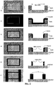
- Figure 2 shows a series of pairs of schematic layout and cross sectional views that illustrate significant steps of a manufacturing process of a conversion structure of the example illustrated in Figure 1 .
- FIG. 2 The views (a) of Figure 2 show schematically a polymer substrate, stable at the process temperatures, on a face of which have been defined narrow rectangular cavities of identical size and orientation, by deposition, masking and anisotropically etching in plasma sacrificial layer of oxide, as were observed in Figure 1 .
- the process continues with the deposition, under highly conformal conditions, for example by chemical deposition process (CVD, LPCVD or alike) carried out in a cold wall reactor , of a polycrystalline electrically conductive layer of conductive material, for example silicon.
- CVD chemical deposition process
- the CVD process is based upon the pyrolitic decomposition of a suitable gaseous precursor, such as for example silane (SiH 4 ) or germane (GeH 4 ) or chlorosilane (SiH n Cl 4-n ) at a temperature of about 600°C and in any case chosen in a temperature range comprised between 500 and 900°C, in presence of also a precursor of the dopant species.
- a highly conformal conductive film with a thickness of about 20 nm, is thus formed as illustrated in (b).
- an anisotropic etching in plasma of the conductor polycrystalline material layer is carried out as far as removing it entirely from “horizontal” surfaces, practically leaving unchanged the thickness of the layer onto the "vertical” surfaces, with respect to the direction of anisotropic etching in plasma.
- the so-formed article can be subjected to a heavy implantation of helium ions in a dose apt to cause the formation of nanobubbles inside the layer of polysilicon of nanometric thickness and which during the heating in oven subsequent to implantation at the highest temperature tolerated by the substrate material and preferably between about 400 and about 900°C, for several hours, will be released from the material at least partially, leaving nanocavities within it.
- Implantation can be repeated at gradually different implantation energies, for example a first implantation at an energy of 50 keV, followed by other implantations with decreasing energies, each implantation performed in doses of about 2 x 10 16 cm 2 , such to form inside the polycrystalline layer nanocavities at different depths, as schematically illustrated in (d).
- the subsequent step of the process contemplates the elimination of the sacrificial oxide layer, that may be easily done by selective wet etching of the oxide against both the substrate polymer and the -crystalline silicon constituting the nanowires rising from the substrate surface, as illustrated in (e).
- the illustrations (f) show the structure being manufactured after having formed a second (non critical) fotoresist mask to define aluminium metal deposition openings over the terminations, on one side and on the other side of the rectangular annular structures of the nanowires and after having removed the masking fotoresist by ashing it.
Landscapes
- Engineering & Computer Science (AREA)
- Manufacturing & Machinery (AREA)
- Silicon Compounds (AREA)
- Investigating Or Analyzing Materials Using Thermal Means (AREA)
- Measuring Temperature Or Quantity Of Heat (AREA)
- Carbon And Carbon Compounds (AREA)
Description
- The invention relates in general to Seebeck/Peltier bidirectional thermoelectric conversion devices and in particular to devices using nanowires of conductor or semiconductor material defined on a substrate with planar technologies.
- Seebeck effect is a thermoelectric phenomenon therefore in a circuit constituted by metallic conductors or semiconductors a temperature difference generates electricity. The effect, discovered by the physicist Thomas J. Seebeck in 1821, appears with the presence of a potential difference at the ends of a metallic bar subjected to a temperature gradient ∇T. In a circuit wherein there are two junctions between two materials A and B placed at temperatures T 1 and T 2 the resulting voltage is given by:

- From the microscopic point of view the charge carriers (electrons in metals, electrons and holes in semiconductors, ions in ionic conductors) will spread when a conductor terminal is at a different temperature respect to the other one. The higher temperature carriers will spread towards the area at lower temperature, as long as there will be different carrier densities in the portion with lower temperature and in the one with higher temperature of the conductor. If the system is isolated, the equilibrium will be reached when, after the scattering process, the heat will uniformly be distributed through the whole conductor. The re-distribution of thermal energy due to the motion of charge carriers is called thermal current, and it is obviously associated to an electric current which will annul when the system temperature will have become uniform. In a system wherein the two junctions vice versa have a constant temperature difference, even the thermal current will be constant and then a constant flow of charge carriers will be noted. The mobility of the carriers is reduced by scattering phenomena (scattering) by the impurities which are present in the lattice, the structural defects and the reticular vibrations (phonons). Therefore, the Seebeck effect in a material depends very significantly upon the density of impurities and upon crystallographic defects of the material apart from the phonon spectrum of the material itself. The phonons, however, are not always in local thermal equilibrium. On the contrary, they move by following the thermal gradient and they lose energy by interacting with the electrons (or other carriers) and with the reticular imperfections. If the phonon-electron interaction is predominant, the phonons tend to push the electrons towards a material portion, loosing energy in the process, thus contributing to the already present electric field. This contribution is even more important in the temperature region wherein the phonon-electron scattering is predominant, that is for

- The performance of a thermoelectric generator can be expressed as1


- From the technological point of view the use of generators based upon the Seebeck effect has been often considered of potential interest. More than half heat produced in a thermal plant is usually dissipated as heat with low enthalpy, it is estimated that about 15 millions of megawatt are wasted only in the energy conversion processes. The availability of Seebeck generators, able to convert only partially such heat in electricity would be able to impact positively on the energy problem.
- However, the thermoelectric generators have an extremely low efficiency. For example, in case of the massive silicon, at room temperature Z ≈ 3×10⁻⁵ K-1; whereas values of ZT ≈ 1 can be obtained only with materials of high cost and reduced availability such as Bi2Te3 or alloys thereof, for example, Sb or Se. In the facts, apart from some uses with high added value such as the thermoelectric generation in spatial environment, the thermoelectric generators based upon massive materials with high availability allow yields of converting thermal power into electric power of only about 7%. By way of comparison a turbine engine is able to convert about 20% of thermal energy into electric current.
- Recently two collaborations operating at University of California in Berkeley2 and of the California Institute of Technology in Pasadena3 have shown that silicon nanowires with sizes transversal to the wire of 20 nm and with properly wrinkled surfaces are characterized by a high thermoelectric figure of merit. The rising of Z derives from the decoupling of the free average paths per phonons and electrons imposed by the scattering to the surfaces. In particular, the important contribution to the thermal conductivity deriving from the acoustic phonons with lower frequency (higher wavelength) is eliminated, thus the density of phonons with higher wavelength than the cross sizes of the wire itself resulting null. Consequently, the silicon thermal conductivity results to be reduced by ≈ 150 W m-1 K-1 (at room temperature per massive Si) at ≈ 1.6 W m-1 K-1 (at room temperature per Si nanowires of 20 nm in section).
- Moreover, the devices implemented by the two collaborations were produced with techniques unsuitable to the industrialization on a big scale. In the approach of the researchers of the University of California in Berkeley2 the nanowires were obtained by chemical etching in baths of AgNO3 and HF, by supplying in uncontrolled way nanowires with diameters variable between 20 and 300 nm (with average value of about 100 nm). The methodology adopted by the researchers of the California Institute of Technology3 uses instead alternatively techniques of lithography with electronic beam or the method of transferring pattern from a superlattice to nanowire (Superlattice Nanowire Pattern Transfer), both extremely complex and expensive; furthermore the control of the surface wrinkledness of the wires results in this case modest and substantially determined by the growth modes.
-
WO2003/046265-A2 andUS2005/112872-A1 both describe nanowires grown from a spot over the surface of a substrate, up to reach and contact electrically a pre-ordered overhanging counter-electrode. Such an approach negates the possibility of forming nanowires of length many order of magnitude greater than the nanometric cross sectional linear dimensions of the nanowires. The nanowires stem from a seeded spot onto the surface of the substrate and grow inside preordered nanoholes defined through an intermediate layer of insulating material. The hot side and cold side of the working thermoelectrical device inevitably coincide with the base electrode (substrate) and the overhanging counter-electrode. Such a technologically limited distance of separation limits the voltage that may be generated between the two electrodes, which is dependent on the difference of temperature that can be maintained on them. - An efficient structure of device for the Seebeck thermoelectric conversion has been found, based upon the use of nanowires of conductor or semiconductor material defined on a substrate with not critical photolithographic definition and by using apparatuses of relatively low cost, on a wide range of substrate materials even with a particularly advantageous cost/performance ratio. In the context of the present description, the term nanowire is meant to indicate a long thin body of electrically conductive or semiconductive material with the most extended meaning as established in the related scientific literature, able to allow the passage of an electrical current in presence of a potential difference between the ends thereof. The section of a nanowire can have any shape with at least a mean linear size or diameter lower than 40nm.
- Basically, a device according to the invention comprises: at least an array of spaced parallel nanowires the section of which has at least a linear size or diameter lower than 40 nm;a substrate of lower electrical conductivity than the electrical conductivity of a material constituting the nanowires, said substrate having a planar surface on which the nanowires are formed;a layer of dielectric material of low heat conductivity and of thickness greater than a height of said nanowires on said substrate surface, filling separation spaces between the parallel nanowires of said array;electrical connection metallizations on the ends of said nanowires, on opposite sides of the array, interconnecting the nanowires in groups of nanowires electrically in parallel and electrically in series to other groups of nanowires connected in parallel and connecting the series-parallel network of nanowires to an external circuit;surfaces coincident with the ends of the nanowires on one side and on the other of said opposite sides of the array constituting surfaces held at different temperatures of the conversion device; wherein said spaced parallel nanowires lay for their whole length onto said planar surface of the substrate; said layer of dielectric material is placed on said substrate surface to fill the separation spaces between parallel nanowires of said array encapsulating the nanowires for their whole length onto the substrate surface.
- The substrate can be made of a material belonging to the group composed by a mono or multi-component glass, a silica aerogel, single-crystal or polycrystalline silicon with null or low concentration of dopants such to have a practically negligible electrical conductivity compared to the electrical conductivity of the material constituting the nanowires, an organic polymeric material resistant to the temperatures of the fabrication process and of operation temperatures of the conversion device, or materials with mechanical, dielectric characteristics equivalent thermal conductivity.
- The features of low thermal conductivity of the substrate material and/or the geometrical shape thereof must be such to minimize each residual behaviour as "thermal bridge" along the longitudinal direction of the parallel nanowires formed on the substrate. Therefore, cellular materials such as aerogels or rigid polymeric and preferably expanded materials are preferred. Other substrates of compact materials may have grooves or transversal cross cavities with respect to the longitudinal axis of the nanowires to reduce the equivalent section of heat transmission.
- The substrate can also be a laminated, wafer or multilayer stack of different materials or be constituted by a wafer of one of the materials mentioned above, wholly coated with a layer of another one of the mentioned materials, for example a monolith of silica aerogel coated with a film of polycrystalline silicon (briefly "polysilicon") of some tens of nanometres up to few micrometers in thickness.
- The structure can be realized with a sequence of process steps which may include a single critical masking step, the definition limit of which (minimum line width) is significantly larger (by at least about one order of magnitude) than the width of the nanowires that are realized. Such nanowires, though theoretically they can be made of any conductive material, according to the present disclosure are made of an element of the IV Group of the Periodic Table, preferably of Si, Ge or alloys thereof doped such to reduce bulk resistivity as far as assuming a value equal or lower than 1Ωcm, deposited by chemical vapour deposition (CVD, LPCVD and the like) in conformal manner way for a thickness from one to few tens of nanometers, on every surface of a sacrificial layer of a material deposited and then photo-lithographically defined on the substrate surface with a first masking step. A subsequent anisotropic etching of the conformally deposited layer removes it from horizontal surfaces, leaving it on vertical surfaces of definition of the sacrificial layer, according to a technique similar to that for forming the so-called dielectric spacers in microelectronics fabrication processes.
- The sacrificial layer, typically a thick layer of oxide, nitride or silicon oxy-nitride of thickness greater than the height of the nanowires to be realized on the substrate surface, can be eliminated for example by dry (in plasma) or selective wet etching, leaving an array of structures of nanometric thickness (nanowires) and height corresponding to the thickness of the sacrificial layer, rising from the substrate surface and extending parallel to each other for the whole longitudinal dimension of the formation area of the substrate surface.
- Obviously, the substrate material must eventually resist to the selective etching solution of the sacrificial layer of oxide and/or nitride. For example, in case of a substrate of glass or silica aerogel, it will need to be coated in advance with a protective film of polysilicon or other material of scarce or null electric conductivity, resistant to the etching solution of the sacrificial layer.
- A dielectric material with reduced thermal conductivity can be then deposited such to fill the separation spaces (trenches) between adjacent nanowires in order to stabilize them mechanically, practically encapsulating the nanowires for their whole length onto the substrate surface. An aerogel made of silica or alumina or other oxide produced by applying and drying on site a sol-gel, represents an optimum stabilization material.
- The two ends of the parallel nanometric structures (nanowires), spaced from one another, of the array thus formed onto an area of the substrate surface or even from one side to the other side of the substrate, are interconnected according to a certain series-parallel scheme and two terminal nodes of the whole series-parallel network of the array nanowires are thence connectable to an electrical circuit external to the bidirectional converter device (to an electrical load or to an electrical source).
- The electrical interconnections of the ends of the parallely extending nanowires can be realized with a second masking step to form openings on the areas coincident with the ends of the nanowires, on one and the other side of the area of formation of the nanowires, and depositing through the mask openings a metal or alloy of low Seebeck coefficient of metallization of the ends of the nanowires and of the separation areas between them on the substrate side. The openings intercept one or more pairs of ends of adjacent nanowires of the array of parallel nanowires along the opposite sides of termination, realizing a designed scheme of series-parallel interconnection and eventually also metallized pads to connect the Seebeck conversion device to an external circuit.
- Through openings thus defined along the two parallel strips that intercept the ends of the nanowires, on one side and on the other one, the connecting metal, for example aluminium or alloy thereof is deposited optionally preceded by a flash deposition of a few nanometers thick compatibilization/adhesion film, for example of tungsten.
- As evident from the above what description, the architecture of the Seebeck thermoelectric conversion device of the present invention allows its realization with common techniques and manufacturing apparatuses of relatively low cost, wherein the separation distance between adjacent nanowires of the array substantially corresponds to the minimum linewidth of photolithographic definition of the sacrificial layer of common manufacturing technologies based upon exposition of a masking photo-resist layer to luminous sources in the ultraviolet region. Nevertheless, the functioning structure of the conversion device has characteristics that make possible commercial production of highly efficient conversion devices at relatively low cost.
- To these important features of the conversion structures of the present invention adds a specific pre-disposition to constitute robust and efficient "stack-like" multimodule architectures adapted to realize converters of relatively high voltage and power capabilities.
- According to an alternative embodiment of the device, the nanowires extend for the whole width of the substrate and they are stabilized by a sufficiently thick layer exceeding the nanowires height over the whole surface of the substrate without performing any second masking or metallization step.
- The surface of the encapsulating layer of silica aerogel may then be planarized by grinding and optionally also by possible lapping the upper surface of the aerogel layer until making it perfectly parallel to the bottom surface of the substrate.
- The so-manufactured thin "tiles" lend themselves to be stacked one onto the other, gluing them, in a way to ensure perfect overlapping of respective corresponding geometrical details, as far as constituting a parallelepiped body constituted by a plurality of single identical modules pre-constituted as described above.
- The two opposite faces of the parallelepiped body coincident with the opposite ends of the nanowires of the arrays of the stacked distinct modules, may be grinded, thus exposing the terminal surfaces of the nanowires.
- On these opposite surfaces of the parallelepiped body may be defined relatively wide vertical or horizontal strips, intercepting the terminal surfaces of a certain number of nanowires, in a perfectly aligned (specular) mode on the two opposite terminal surfaces of the nanowires of all the stacked modules. On the strip areas a deposited metal layer, for example of aluminium, will short-circuit, on one and the other side, a certain number of nanowire ends of each module and eventually of homologous nanowires of the other stacked modules.
- By connecting in series the groups of nanowires in parallel by wires or strips of metal defined on other two of sides of the parallelepiped body (on other elevation sides of the nanowires have been connected in parallel by defining "horizontal" strips of metal or on the upper surface and on the bottom surface if the nanowires have been connected in parallel by defining "vertical" strips of metal), an interconnection scheme of groups of nanowires in parallel, in series to other groups of nanowires in parallel according to a desired scheme, can be easily realized, in order to obtain at the terminals of the series/parallel network a sum voltage of the developed Seebeck voltage at the actual conditions of temperature difference of the two sensible sides of the device, at the two ends of the single nanowires, as well as a multiplied capability of deliverable current.
- Definition of relatively wide areas on the two termination sides of the nanowires (the sensible sides of the Seebeck converter) and on the other pair of sides (for connecting in series groups of nanowires) of deposition of the contacting and connecting metal layer, allows the use of less sophisticated techniques for defining a suitable resist mask than those usually used to define micrometric or sub-micrometric openings.
- Moreover, it has been observed that the way of forming the nanowires by anisotropic etching in plasma of a conformally deposited matrix layer produces wrinkles on the "vertical" surface of the nanowires exposed to the plasma which increases significantly the thermoelectric figure of merit by favouring an enhanced decoupling of the mean free path figures relative to phonons and to electrons because of scattering effects at surfaces.
- Furthermore, it has been found that the nanowires of the arrays of the present invention can be subjected to a heavy implant of not reactive gaseous elements, such as for example helium. A subsequent heating of the implanted nanowires causes the formation of layers of nanobubbles at helium implantation depths that may be altered during implantation (using different kinetic energies of the ions). Formation of nanocavities in the material constituting the nanowires increases significantly the scattering of phonons contrasting heat conduction along the longitudinal direction of the nanowires without materially decreasing the electrical conductivity thereof.
- The invention is more precisely defined by the annexed claims.
-
Figure 1 is a layout schematic view of a Seebeck conversion device according to an embodiment of the present invention. -
Figure 2 illustrates some phases of the manufacturing process of the device structure offigure 1 . -
Figure 1 is a layout schematic view of an exemplary conversion structure of a device of the invention. - The
substrate 1 can be a polymeric sheet resistant to high temperatures. - In the illustrated scheme can be observed the array of nanowires of
polycrystalline silicon 2, extending parallel and uniformly spaced from one side to the other of a surface of thesubstrate 1, According to the illustrated example, the array of nanowires is constituted by a plurality of rectangular rings of heavily doped polysilicon such an electric resistivity not in exess of 1 Qcm, a thickness (width) of about 20 nanometers and height of about 40 nanometers. - Uninterrupted strips of metal along opposite terminal areas of the rectangular rings of
nanowires 2, connect in parallel groups of sixnanowires 2 of the array. - Metallization of the opposite ends of the
nanowires 2 is done using a specific non critical mask, defining aligned openings through which a metal ormetal alloy 3, preferably with a low Seebeck coefficient, for example aluminium is deposited, on the areas identified by phantom dotted line, thus short-circuiting the ends of the nanowires on one side and on the other side of the structure. Wires ofelectrical connection 4 may be bonded to the metal layer, in order to connect in series adjacent groups of nanowires and, in case the two extreme groups of the electrical series to terminal pads adapted to connect the conversion device to an external circuit. - The opposite end surfaces of the so-implemented array of parallel nanowires are thermally coupled to a hot wall and to a cold wall, respectively, for generating by Seebeck effect, a voltage corresponding to the Seebeck voltage induced by the temperature difference on each
nanowire 2, multiplied by the number of groups of nanowires electrically connected in series between two terminals connecting the converter to an external load. - Obviously, the converter device is bidirectional, as it can operate as voltage generator or as heat pump by forcing with an electric current along the nanowires with an external electrical source causing heat extraction from a wall (being cooled) to the other wall (being heated).
-
Figure 2 shows a series of pairs of schematic layout and cross sectional views that illustrate significant steps of a manufacturing process of a conversion structure of the example illustrated inFigure 1 . - The views (a) of
Figure 2 show schematically a polymer substrate, stable at the process temperatures, on a face of which have been defined narrow rectangular cavities of identical size and orientation, by deposition, masking and anisotropically etching in plasma sacrificial layer of oxide, as were observed inFigure 1 . - The process continues with the deposition, under highly conformal conditions, for example by chemical deposition process (CVD, LPCVD or alike) carried out in a cold wall reactor , of a polycrystalline electrically conductive layer of conductive material, for example silicon. According to common practice, the CVD process is based upon the pyrolitic decomposition of a suitable gaseous precursor, such as for example silane (SiH4) or germane (GeH4) or chlorosilane (SiHnCl4-n) at a temperature of about 600°C and in any case chosen in a temperature range comprised between 500 and 900°C, in presence of also a precursor of the dopant species. A highly conformal conductive film with a thickness of about 20 nm, is thus formed as illustrated in (b).
- As illustrated in (c), an anisotropic etching in plasma of the conductor polycrystalline material layer is carried out as far as removing it entirely from "horizontal" surfaces, practically leaving unchanged the thickness of the layer onto the "vertical" surfaces, with respect to the direction of anisotropic etching in plasma.
- Optionally, the so-formed article can be subjected to a heavy implantation of helium ions in a dose apt to cause the formation of nanobubbles inside the layer of polysilicon of nanometric thickness and which during the heating in oven subsequent to implantation at the highest temperature tolerated by the substrate material and preferably between about 400 and about 900°C, for several hours, will be released from the material at least partially, leaving nanocavities within it. Implantation can be repeated at gradually different implantation energies, for example a first implantation at an energy of 50 keV, followed by other implantations with decreasing energies, each implantation performed in doses of about 2 x 1016 cm2, such to form inside the polycrystalline layer nanocavities at different depths, as schematically illustrated in (d).
- The subsequent step of the process contemplates the elimination of the sacrificial oxide layer, that may be easily done by selective wet etching of the oxide against both the substrate polymer and the -crystalline silicon constituting the nanowires rising from the substrate surface, as illustrated in (e).
- It is even possible to conformally deposit the mother layer of electrically conductive material from which the elements of nanometric thickness (nanowires) will be obtained with a larger width, such to allow repeated implantations of helium ions at different implantation energies as described above, for reducing the risk of causing fractures or failures of the residual "spacers" on the "vertical" surfaces of definition the sacrificial oxide layer and, only when the treatment is completed, conducting an additional anisotropic etching in plasma with a not null incidence angle with respect to the vertical axis, for reducing the over-dimensioning of the thickness of the spacers to the wished nanometric size of the nanowires already subjected to energetic implantation and release of helium.
- The illustrations (f) show the structure being manufactured after having formed a second (non critical) fotoresist mask to define aluminium metal deposition openings over the terminations, on one side and on the other side of the rectangular annular structures of the nanowires and after having removed the masking fotoresist by ashing it.
- At this point, deposition of a stabilization layer according to what previously described will follow.
-
- 1 D. K. C. MacDonald, Thermoelectricity: An Introduction to the Principles (Wiley, New York, 1962).
- 2 A. I. Hochbaum, R. K. Chen, R. D. Delgado, W. J. Liang, E. C. Garnett, M. Najarian, A. Majumdar, and P. D. Yang, Nature 451, 163-U5 (2008).
- 3 A. I. Boukai, Y. Bunimovich, J. Tahir-Kheli, J.-K. Yu, W. A. Goddard Iii, and J. R. Heath, Nature 451, 168-171 (2008).
- 4 G. F. Cerofolini, G. Arena, M. Camalleri, C. Galati, S. Reina, L. Renna, D. Mascolo, and V. Nosik, Microelectronic Engineering 81, 405-419 (2005).
- 5 G. F. Cerofolini, G. Arena, C. M. Camalleri, C. Galati, S. Reina, L. Renna, and D. Mascolo, Nanotechnology 16, 1040-1047 (2005).
- 6 Y. K. Choi, J. S. Lee, J. Zhu, G. A. Somorjai, L. P. Lee, and J. Bokor, Journal of Vacuum Science & Technology B 21, 2951-2955 (2003).
- 7 Y. K. Choi, J. Zhu, J. Grunes, J. Bokor, and G. A. Somorjai, Journal of Physical Chemistry B 107, 3340-3343 (2003).
- 8 D. C. Flanders and N. N. Efremow, Journal of Vacuum Science & ).
- 9 W. R. Hunter, T. C. Holloway, P. K. Chatterjee, and A. F. Tasch, Jr., IEEE Electron Device Letters EDL-2, 4-6 (1981).
- 10 G. F. Cerofolini, Nanotechnology E-Newsletter 7, 5 (2005).
- 11 R. Tonini, F. Corni, S. Frabboni, G. Ottaviani, and G. F. Cerofolini, Journal of Applied Physics 84, 4802-4808 (1998).
Claims (14)
- A Seebeck/Peltier effect bidirectional thermoelectric conversion device using nanowires (2) on a substrate (1), comprising:at least an array of spaced parallel nanowires the section of which has at least a linear size or diameter lower than 40 nm;a substrate of lower electrical conductivity than the electrical conductivity of a material constituting the nanowires, said substrate having a planar surface on which the nanowires are formed;a layer of dielectric material of low heat conductivity and of thickness greater than a height of said nanowires on said substrate surface, filling separation spaces between the parallel nanowires of said array;electrical connection metallizations (3) on the ends of said nanowires, on opposite sides of the array, interconnecting the nanowires in groups of nanowires electrically in parallel and electrically in series to other groups of nanowires connected in parallel and connecting the series-parallel network of nanowires to an external circuit;surfaces coincident with the ends of the nanowires on one side and on the other of said opposite sides of the array constituting surfaces held at different temperatures of the conversion device;characterized in that
said spaced parallel nanowires lay for their whole length onto said planar surface of the substrate; said layer of dielectric material is placed on said substrate surface to fill the separation spaces between parallel nanowires of said array encapsulating the nanowires for their whole length onto the substrate surface. - The device according to claim 1, characterized in that said substrate comprises a material belonging to the group composed by mono or multi-component glass, silica aerogel, silicon without or with a low concentration of dopants, polymeric materials resistant to process and functioning temperatures of the conversion device.
- The device according to claim 2, wherein said substrate is a monolith of silica aerogel coated with a film of undoped polycristalline silicon.
- The device according to claim 2, wherein said substrate is a stiff organic polymeric monolith.
- The device according to claim 4, wherein said stiff monolith is of expanded organic polymer.
- The device according to claim 2, wherein said substrate is a monolith of compact material having a plurality of grooves on its lower face or inner cavities transversal to the longitudinal direction of said nanowires formed on its upper face.
- The device according to claim 1, characterized in that the nanowires are of a material belonging to the IV group of the Periodic System or alloys of elements belonging to the IV group of the periodic system, with a dopant concentration adapted to confer to the material an electrical resistivity lower than 1 Ω cm.
- The device according to claim 1, characterized in that said filler dielectric material of low heat conductivity is an aerogel of silica or alumina or other oxide produced by application and drying of a sol-gel.
- The conversion device according to claim 1, characterized in that said electrical connection metallizations are of a metal or metallic alloy having a low Seebeck coefficient.
- The conversion device according to claim 9, characterized in that it comprises a few nm thick adhesion/compatibilization conductive pre-layer of a transition metal between the material constituting the nanowire and the metal or metallic alloy of electrical connection.
- The device according to claim 1, wherein the nanowire material has inner nanocavities obtained by implanting Helium in the nanowire material and subsequently heating the implanted material.
- The device according to claim 1, characterized in that it comprises a stack of a number of identical device modules, stacked to form a parallelepiped body, on opposite faces of which surface the ends of the conductive nanowires of the arrays of all said identical device modules stacked in reciprocal alignment, defined strips of metal on one and on the other of said opposite faces of the parallelepiped body apt to connect in parallel groups of homologous nanowires of distinct arrays and in series said groups between two terminals for connecting to an external outer circuit the so-constituted series-parallel network of nanowires.
- Method of fabricating a Seebeck/Peltier effect bidirectional thermoelectric conversion device according to claim 1 using nanowires on a substrate of lower electrical conductivity compared to the electrical conductivity of the material constituting the nanowires, the method comprising the steps of conformally depositing on the whole formation area of said array of nanowires after having defined thereon by photolithography parallel channels with vertical etch surfaces in a sacrificial layer of uniform thickness not lower than the height of nanowires to be formed, a layer of a material belonging to the group composed by silicon oxide, silicon oxy-nitride and silicon nitride or mixtures of the same, and subsequent anisotropically etching in plasma the conformally deposited layer of the material constituting the nanowires over the planar surface, and removing residues of said photolithographically defined sacrificial layer by selective wet etching.
- The method of claim 13, wherein the separation distance between adjacent nanowires of said array corresponds to the minimum linewidth of photolithographic definition of the sacrificial layer of the manufacturing technology.
Applications Claiming Priority (2)
| Application Number | Priority Date | Filing Date | Title |
|---|---|---|---|
| IT000193A ITRM20080193A1 (en) | 2008-04-11 | 2008-04-11 | THERMO-ELECTRIC BIDIRECTIONAL CONVERSION DEVICE WITH EFFECT SEEBECK / PELTIER USING NANOFILES OF CONDUCTOR OR SEMICONDUCTOR MATERIAL. |
| PCT/IB2009/051390 WO2009125317A2 (en) | 2008-04-11 | 2009-04-02 | Seebeck/peltier bidirectional thermo- electric conversion device using nanowires of conductor or semiconductor material |
Publications (2)
| Publication Number | Publication Date |
|---|---|
| EP2277209A2 EP2277209A2 (en) | 2011-01-26 |
| EP2277209B1 true EP2277209B1 (en) | 2019-12-25 |
Family
ID=40297218
Family Applications (1)
| Application Number | Title | Priority Date | Filing Date |
|---|---|---|---|
| EP09729659.4A Active EP2277209B1 (en) | 2008-04-11 | 2009-04-02 | Seebeck/peltier bidirectional thermo- electric conversion device using nanowires of conductor or semiconductor material |
Country Status (6)
| Country | Link |
|---|---|
| US (1) | US9484517B2 (en) |
| EP (1) | EP2277209B1 (en) |
| JP (1) | JP5677710B2 (en) |
| CN (1) | CN102057512B (en) |
| IT (1) | ITRM20080193A1 (en) |
| WO (1) | WO2009125317A2 (en) |
Families Citing this family (42)
| Publication number | Priority date | Publication date | Assignee | Title |
|---|---|---|---|---|
| CN104392933B (en) | 2007-08-21 | 2017-11-07 | 加州大学评议会 | Nanostructured with high-performance thermoelectric property |
| US9978924B2 (en) | 2009-10-09 | 2018-05-22 | Toyota Jidosha Kabushiki Kaisha | Method of producing thermoelectric material |
| US9755128B2 (en) | 2008-10-10 | 2017-09-05 | Toyota Motor Engineering & Manufacturing North America, Inc. | Method of producing thermoelectric material |
| JP5282598B2 (en) * | 2009-02-17 | 2013-09-04 | 富士通株式会社 | Method for manufacturing thermoelectric conversion element |
| IT1397598B1 (en) | 2009-07-15 | 2013-01-16 | Univ Milano Bicocca | THERMO-ELECTRIC CONVERSION DEVICE WITH EFFECT SEEBECK / PELTIER USING STRUCTURES OF SEMICONDUCTIVE MATERIAL TREATED NOT REQUESTING DEFINITION ON NANOMETRIC SCALE |
| IT1397679B1 (en) * | 2009-12-15 | 2013-01-18 | Univ Milano Bicocca | THERMO-ELECTRIC CONVERSION ELEMENT SEEBECK / PELTIER INCLUDING PARALLEL NANOFILES OF CONDUCTOR OR SEMICONDUCTOR MATERIALS ORGANIZED IN FILE AND COLUMNS THROUGH AN INSULATING BODY AND PROCEDURE |
| KR101352362B1 (en) * | 2010-02-16 | 2014-01-15 | 한국전자통신연구원 | Thermoelectric device and method of forming the same, temperature sensing sensor, and heat-source image sensor using the same |
| JP2011171716A (en) * | 2010-02-16 | 2011-09-01 | Korea Electronics Telecommun | Thermoelectric device, method of forming the same, and temperature sensing sensor and heat-source image sensor using the same |
| US9240328B2 (en) * | 2010-11-19 | 2016-01-19 | Alphabet Energy, Inc. | Arrays of long nanostructures in semiconductor materials and methods thereof |
| US8736011B2 (en) | 2010-12-03 | 2014-05-27 | Alphabet Energy, Inc. | Low thermal conductivity matrices with embedded nanostructures and methods thereof |
| WO2012101312A1 (en) * | 2011-01-25 | 2012-08-02 | Consejo Superior De Investigaciones Científicas | Method for the production of a thermoelectric device and resulting thermoelectric device |
| ITMI20110751A1 (en) | 2011-05-04 | 2012-11-05 | Consorzio Delta Ti Res | THERMOELECTRIC CONVERSION SEEBECK / PELTIER USING ALTERNATE STAINED NANOMETRIC LAYERS OF CONDUCTOR AND DIELECTRIC MATERIAL AND MANUFACTURING PROCEDURE |
| ITMI20111558A1 (en) | 2011-08-30 | 2013-03-01 | Consorzio Delta Ti Res | THERMOELECTRIC CONVERSION SEEBECK / PELTIER WITH FONONI CONFINEMENT CRYSTALLINE SEMICONDUCTOR LAYERS CONTAINING ANGSTROM-DIMENSIONAL ORGANIC GROUPS AS REPLACEMENT OF SEMICONDUCTOR ATOMES IN CRYSTALLINE AND PRO |
| ITRM20110472A1 (en) | 2011-09-09 | 2013-03-10 | Consorzio Delta Ti Res | MICROELECTRONIC COMPONENTS, IN PARTICULAR CMOS CIRCUITS, INCLUDING THERMO-ELECTRIC ELEMENTS OF SEEBECK / PELTIER EFFECT COOLING, INTEGRATED IN THEIR STRUCTURE. |
| US9051175B2 (en) | 2012-03-07 | 2015-06-09 | Alphabet Energy, Inc. | Bulk nano-ribbon and/or nano-porous structures for thermoelectric devices and methods for making the same |
| US9257627B2 (en) | 2012-07-23 | 2016-02-09 | Alphabet Energy, Inc. | Method and structure for thermoelectric unicouple assembly |
| EP2790474B1 (en) * | 2013-04-09 | 2016-03-16 | Harman Becker Automotive Systems GmbH | Thermoelectric cooler/heater integrated in printed circuit board |
| US9040339B2 (en) | 2013-10-01 | 2015-05-26 | The Pen | Practical method of producing an aerogel composite continuous thin film thermoelectric semiconductor material |
| US9276190B2 (en) | 2013-10-01 | 2016-03-01 | The Pen | Practical method of producing an aerogel composite continuous thin film thermoelectric semiconductor material by modified MOCVD |
| WO2015157501A1 (en) | 2014-04-10 | 2015-10-15 | Alphabet Energy, Inc. | Ultra-long silicon nanostructures, and methods of forming and transferring the same |
| CN104009149A (en) * | 2014-06-10 | 2014-08-27 | 四川航天系统工程研究所 | Semiconductor refrigeration device and manufacturing method thereof |
| US10720560B2 (en) | 2014-09-11 | 2020-07-21 | Northwestern University | System and method for nanowire-array transverse thermoelectrics |
| EP3198648B1 (en) | 2014-09-22 | 2018-07-25 | Consorzio Delta Ti Research | Silicon integrated, out-of-plane heat flux thermoelectric generator |
| JP6862339B2 (en) | 2014-10-01 | 2021-04-21 | コンソルツィオ デルタ ティ リサーチ | Silicon integrated bi-valve thermoelectric generator with out-of-plane heat flux configuration |
| CN107078202B (en) * | 2014-10-09 | 2019-07-19 | 德尔塔蒂研究财团 | An integrated thermoelectric generator |
| KR102250190B1 (en) * | 2014-10-31 | 2021-05-10 | 삼성전자주식회사 | Graphene structure having nanobubbles and method of fabricating the same |
| CN104372900B (en) * | 2014-11-11 | 2016-06-22 | 福建工程学院 | The solar energy house plane system of a kind of multifunctional all and control method |
| FR3030889B1 (en) * | 2014-12-19 | 2017-01-27 | Commissariat Energie Atomique | DIFFERENTIAL TEMPERATURE SENSOR. |
| CN104851965A (en) * | 2015-03-29 | 2015-08-19 | 四川师范大学 | New method using bismuth telluride-doped carbon aerogel to prepare thermoelectric material |
| WO2018028772A1 (en) | 2016-08-10 | 2018-02-15 | Politecnico Di Milano | Active material and electric power generator containing it |
| IT201600109345A1 (en) | 2016-10-28 | 2018-04-28 | Consorzio Delta Ti Res | Integrated thermoelectric generator and relative manufacturing method |
| WO2019120509A1 (en) | 2017-12-20 | 2019-06-27 | Termo-Ind S.A. | Active material and electric power generator containing it |
| IT201800002541A1 (en) | 2018-02-09 | 2019-08-09 | Termo Ind Sa | ACTIVE MATERIAL AND ELECTRICAL POWER GENERATOR CONTAINING THE SAME |
| US20210101009A1 (en) * | 2018-02-19 | 2021-04-08 | The General Hospital Corporation | Systems and methods for ultra-focal transcranial magnetic stimulation |
| US12181351B2 (en) * | 2018-02-28 | 2024-12-31 | Arthur Beckman | Thermopile assembly providing a massive electrical series of wire thermocouple elements |
| GB201913701D0 (en) | 2019-09-23 | 2019-11-06 | Crayonano As | Composition of matter |
| TWI744717B (en) * | 2019-11-13 | 2021-11-01 | 銀河製版印刷有限公司 | Thermoelectric power generating device and manufacturing method thereof |
| IT202000001879A1 (en) * | 2020-01-31 | 2021-07-31 | St Microelectronics Srl | Thermoelectric generator |
| WO2022128129A1 (en) | 2020-12-18 | 2022-06-23 | Politecnico Di Milano | Electric power generator containing an active organic material |
| CN116867345B (en) * | 2022-08-04 | 2026-04-24 | 三峡大学 | P-type and N-type semiconductor hybrid array thermoelectric devices for improved power and performance |
| SE547640C2 (en) * | 2024-04-09 | 2025-11-04 | Jondetech Sensors Ab Publ | Nanowire based lead for thermopile |
| CN119907616B (en) * | 2025-01-15 | 2026-02-13 | 哈尔滨工业大学 | High-temperature waste heat recovery system based on space-associated disordered silicon germanium nanowires |
Family Cites Families (19)
| Publication number | Priority date | Publication date | Assignee | Title |
|---|---|---|---|---|
| US3261079A (en) * | 1962-09-10 | 1966-07-19 | Texas Instruments Inc | Fabrication of thermoelectric apparatus |
| US5022928A (en) * | 1985-10-04 | 1991-06-11 | Buist Richard J | Thermoelectric heat pump/power source device |
| US5994164A (en) * | 1997-03-18 | 1999-11-30 | The Penn State Research Foundation | Nanostructure tailoring of material properties using controlled crystallization |
| JP3447915B2 (en) * | 1997-04-28 | 2003-09-16 | シャープ株式会社 | Thermoelectric element and thermoelectric element module using the same |
| JPH1168173A (en) | 1997-08-08 | 1999-03-09 | Komatsu Ltd | Heat exchanger using thermoelectric module |
| JP3463657B2 (en) * | 2000-07-24 | 2003-11-05 | 株式会社村田製作所 | Infrared sensor |
| WO2003046265A2 (en) * | 2001-11-26 | 2003-06-05 | Massachusetts Institute Of Technology | Thick porous anodic alumina films and nanowire arrays grown on a solid substrate |
| US20040123489A1 (en) * | 2002-04-22 | 2004-07-01 | The Procter & Gamble Company | Thermal protection of fabric article treating device |
| JP2004056866A (en) | 2002-07-17 | 2004-02-19 | Nec Engineering Ltd | Mobile communication device with power generation function |
| JP2004241397A (en) | 2003-01-23 | 2004-08-26 | Dainippon Printing Co Ltd | Thin film transistor and manufacturing method thereof |
| CN100397671C (en) * | 2003-10-29 | 2008-06-25 | 京瓷株式会社 | Thermoelectric conversion module |
| US6969679B2 (en) * | 2003-11-25 | 2005-11-29 | Canon Kabushiki Kaisha | Fabrication of nanoscale thermoelectric devices |
| US7465871B2 (en) * | 2004-10-29 | 2008-12-16 | Massachusetts Institute Of Technology | Nanocomposites with high thermoelectric figures of merit |
| US8541678B2 (en) * | 2005-03-14 | 2013-09-24 | Borealis Technical Limited | Thermionic/thermotunneling thermo-electrical converter |
| JP2006269763A (en) | 2005-03-24 | 2006-10-05 | Toshiba Corp | Method for manufacturing integrated circuit device |
| US8039726B2 (en) * | 2005-05-26 | 2011-10-18 | General Electric Company | Thermal transfer and power generation devices and methods of making the same |
| JP2007059773A (en) * | 2005-08-26 | 2007-03-08 | Matsushita Electric Ind Co Ltd | Thermoelectric conversion element and manufacturing method thereof |
| US20070277866A1 (en) * | 2006-05-31 | 2007-12-06 | General Electric Company | Thermoelectric nanotube arrays |
| JP2008010704A (en) | 2006-06-30 | 2008-01-17 | Sanyo Electric Co Ltd | Thermoelectric device |
-
2008
- 2008-04-11 IT IT000193A patent/ITRM20080193A1/en unknown
-
2009
- 2009-04-02 WO PCT/IB2009/051390 patent/WO2009125317A2/en not_active Ceased
- 2009-04-02 CN CN200980121457.5A patent/CN102057512B/en not_active Expired - Fee Related
- 2009-04-02 JP JP2011503524A patent/JP5677710B2/en not_active Expired - Fee Related
- 2009-04-02 US US12/937,058 patent/US9484517B2/en not_active Expired - Fee Related
- 2009-04-02 EP EP09729659.4A patent/EP2277209B1/en active Active
Non-Patent Citations (1)
| Title |
|---|
| None * |
Also Published As
| Publication number | Publication date |
|---|---|
| JP5677710B2 (en) | 2015-02-25 |
| CN102057512B (en) | 2014-11-19 |
| CN102057512A (en) | 2011-05-11 |
| ITRM20080193A1 (en) | 2009-10-12 |
| US20110083713A1 (en) | 2011-04-14 |
| EP2277209A2 (en) | 2011-01-26 |
| WO2009125317A2 (en) | 2009-10-15 |
| WO2009125317A3 (en) | 2010-04-01 |
| US9484517B2 (en) | 2016-11-01 |
| JP2011517109A (en) | 2011-05-26 |
Similar Documents
| Publication | Publication Date | Title |
|---|---|---|
| US9484517B2 (en) | Seebeck/peltier bidirectional thermoelectric conversion device using nanowires of conductive or semiconductive material | |
| JP5677713B2 (en) | Thermal-electrical conversion device using the Savebeck / Pelty effect using processed layers made of semiconductor material without the need for nanostructures | |
| JP5988302B2 (en) | Thermoelectric conversion device using the Savebeck / Peltier effect, comprising parallel nanowires made of a conductive material or a semiconductor material arranged in rows and columns via an insulating material, and a method of manufacturing the same | |
| US8736011B2 (en) | Low thermal conductivity matrices with embedded nanostructures and methods thereof | |
| US20120247527A1 (en) | Electrode structures for arrays of nanostructures and methods thereof | |
| US20050112872A1 (en) | Fabrication of nanoscale thermoelectric devices | |
| CN102769099B (en) | Use alternately Seebeck/Pa Er note thermoelectric conversion element and the preparation method of the stacked body of nanometer layer of conductibility and dielectric substance | |
| US8809667B2 (en) | Thermoelectric semiconductor component | |
| EP3750195A1 (en) | Thermoelectric devices based on nanophononic metamaterials | |
| US20140130839A1 (en) | Structure useful for producing a thermoelectric generator, thermoelectric generator comprising same and method for producing same | |
| Trung et al. | Flexible thermoelectric power generators based on electrochemical deposition process of BI 2 TE 3 and SB 2 TE 3 | |
| Cerofolini et al. | Industrially Scalable Process for Silicon Nanowires | |
| Kochergin | High Efficiency Thermoelectric Materials and Devices |
Legal Events
| Date | Code | Title | Description |
|---|---|---|---|
| PUAI | Public reference made under article 153(3) epc to a published international application that has entered the european phase |
Free format text: ORIGINAL CODE: 0009012 |
|
| 17P | Request for examination filed |
Effective date: 20101104 |
|
| AK | Designated contracting states |
Kind code of ref document: A2 Designated state(s): AT BE BG CH CY CZ DE DK EE ES FI FR GB GR HR HU IE IS IT LI LT LU LV MC MK MT NL NO PL PT RO SE SI SK TR |
|
| AX | Request for extension of the european patent |
Extension state: AL BA RS |
|
| DAX | Request for extension of the european patent (deleted) | ||
| RAP1 | Party data changed (applicant data changed or rights of an application transferred) |
Owner name: CONSORZIO DELTA TI RESEARCH |
|
| 17Q | First examination report despatched |
Effective date: 20140731 |
|
| STAA | Information on the status of an ep patent application or granted ep patent |
Free format text: STATUS: EXAMINATION IS IN PROGRESS |
|
| GRAP | Despatch of communication of intention to grant a patent |
Free format text: ORIGINAL CODE: EPIDOSNIGR1 |
|
| STAA | Information on the status of an ep patent application or granted ep patent |
Free format text: STATUS: GRANT OF PATENT IS INTENDED |
|
| INTG | Intention to grant announced |
Effective date: 20190724 |
|
| GRAS | Grant fee paid |
Free format text: ORIGINAL CODE: EPIDOSNIGR3 |
|
| GRAA | (expected) grant |
Free format text: ORIGINAL CODE: 0009210 |
|
| STAA | Information on the status of an ep patent application or granted ep patent |
Free format text: STATUS: THE PATENT HAS BEEN GRANTED |
|
| AK | Designated contracting states |
Kind code of ref document: B1 Designated state(s): AT BE BG CH CY CZ DE DK EE ES FI FR GB GR HR HU IE IS IT LI LT LU LV MC MK MT NL NO PL PT RO SE SI SK TR |
|
| REG | Reference to a national code |
Ref country code: GB Ref legal event code: FG4D |
|
| REG | Reference to a national code |
Ref country code: CH Ref legal event code: EP |
|
| REG | Reference to a national code |
Ref country code: AT Ref legal event code: REF Ref document number: 1218094 Country of ref document: AT Kind code of ref document: T Effective date: 20200115 |
|
| REG | Reference to a national code |
Ref country code: DE Ref legal event code: R096 Ref document number: 602009060803 Country of ref document: DE |
|
| REG | Reference to a national code |
Ref country code: IE Ref legal event code: FG4D |
|
| REG | Reference to a national code |
Ref country code: NL Ref legal event code: MP Effective date: 20191225 |
|
| PG25 | Lapsed in a contracting state [announced via postgrant information from national office to epo] |
Ref country code: FI Free format text: LAPSE BECAUSE OF FAILURE TO SUBMIT A TRANSLATION OF THE DESCRIPTION OR TO PAY THE FEE WITHIN THE PRESCRIBED TIME-LIMIT Effective date: 20191225 Ref country code: BG Free format text: LAPSE BECAUSE OF FAILURE TO SUBMIT A TRANSLATION OF THE DESCRIPTION OR TO PAY THE FEE WITHIN THE PRESCRIBED TIME-LIMIT Effective date: 20200325 Ref country code: LT Free format text: LAPSE BECAUSE OF FAILURE TO SUBMIT A TRANSLATION OF THE DESCRIPTION OR TO PAY THE FEE WITHIN THE PRESCRIBED TIME-LIMIT Effective date: 20191225 Ref country code: NO Free format text: LAPSE BECAUSE OF FAILURE TO SUBMIT A TRANSLATION OF THE DESCRIPTION OR TO PAY THE FEE WITHIN THE PRESCRIBED TIME-LIMIT Effective date: 20200325 Ref country code: GR Free format text: LAPSE BECAUSE OF FAILURE TO SUBMIT A TRANSLATION OF THE DESCRIPTION OR TO PAY THE FEE WITHIN THE PRESCRIBED TIME-LIMIT Effective date: 20200326 Ref country code: SE Free format text: LAPSE BECAUSE OF FAILURE TO SUBMIT A TRANSLATION OF THE DESCRIPTION OR TO PAY THE FEE WITHIN THE PRESCRIBED TIME-LIMIT Effective date: 20191225 Ref country code: LV Free format text: LAPSE BECAUSE OF FAILURE TO SUBMIT A TRANSLATION OF THE DESCRIPTION OR TO PAY THE FEE WITHIN THE PRESCRIBED TIME-LIMIT Effective date: 20191225 |
|
| REG | Reference to a national code |
Ref country code: LT Ref legal event code: MG4D |
|
| PG25 | Lapsed in a contracting state [announced via postgrant information from national office to epo] |
Ref country code: HR Free format text: LAPSE BECAUSE OF FAILURE TO SUBMIT A TRANSLATION OF THE DESCRIPTION OR TO PAY THE FEE WITHIN THE PRESCRIBED TIME-LIMIT Effective date: 20191225 |
|
| PG25 | Lapsed in a contracting state [announced via postgrant information from national office to epo] |
Ref country code: CZ Free format text: LAPSE BECAUSE OF FAILURE TO SUBMIT A TRANSLATION OF THE DESCRIPTION OR TO PAY THE FEE WITHIN THE PRESCRIBED TIME-LIMIT Effective date: 20191225 Ref country code: NL Free format text: LAPSE BECAUSE OF FAILURE TO SUBMIT A TRANSLATION OF THE DESCRIPTION OR TO PAY THE FEE WITHIN THE PRESCRIBED TIME-LIMIT Effective date: 20191225 Ref country code: RO Free format text: LAPSE BECAUSE OF FAILURE TO SUBMIT A TRANSLATION OF THE DESCRIPTION OR TO PAY THE FEE WITHIN THE PRESCRIBED TIME-LIMIT Effective date: 20191225 Ref country code: PT Free format text: LAPSE BECAUSE OF FAILURE TO SUBMIT A TRANSLATION OF THE DESCRIPTION OR TO PAY THE FEE WITHIN THE PRESCRIBED TIME-LIMIT Effective date: 20200520 Ref country code: EE Free format text: LAPSE BECAUSE OF FAILURE TO SUBMIT A TRANSLATION OF THE DESCRIPTION OR TO PAY THE FEE WITHIN THE PRESCRIBED TIME-LIMIT Effective date: 20191225 |
|
| PG25 | Lapsed in a contracting state [announced via postgrant information from national office to epo] |
Ref country code: IS Free format text: LAPSE BECAUSE OF FAILURE TO SUBMIT A TRANSLATION OF THE DESCRIPTION OR TO PAY THE FEE WITHIN THE PRESCRIBED TIME-LIMIT Effective date: 20200425 Ref country code: SK Free format text: LAPSE BECAUSE OF FAILURE TO SUBMIT A TRANSLATION OF THE DESCRIPTION OR TO PAY THE FEE WITHIN THE PRESCRIBED TIME-LIMIT Effective date: 20191225 |
|
| REG | Reference to a national code |
Ref country code: DE Ref legal event code: R097 Ref document number: 602009060803 Country of ref document: DE |
|
| PG25 | Lapsed in a contracting state [announced via postgrant information from national office to epo] |
Ref country code: ES Free format text: LAPSE BECAUSE OF FAILURE TO SUBMIT A TRANSLATION OF THE DESCRIPTION OR TO PAY THE FEE WITHIN THE PRESCRIBED TIME-LIMIT Effective date: 20191225 Ref country code: DK Free format text: LAPSE BECAUSE OF FAILURE TO SUBMIT A TRANSLATION OF THE DESCRIPTION OR TO PAY THE FEE WITHIN THE PRESCRIBED TIME-LIMIT Effective date: 20191225 |
|
| PLBE | No opposition filed within time limit |
Free format text: ORIGINAL CODE: 0009261 |
|
| STAA | Information on the status of an ep patent application or granted ep patent |
Free format text: STATUS: NO OPPOSITION FILED WITHIN TIME LIMIT |
|
| REG | Reference to a national code |
Ref country code: AT Ref legal event code: MK05 Ref document number: 1218094 Country of ref document: AT Kind code of ref document: T Effective date: 20191225 |
|
| PG25 | Lapsed in a contracting state [announced via postgrant information from national office to epo] |
Ref country code: MC Free format text: LAPSE BECAUSE OF FAILURE TO SUBMIT A TRANSLATION OF THE DESCRIPTION OR TO PAY THE FEE WITHIN THE PRESCRIBED TIME-LIMIT Effective date: 20191225 Ref country code: SI Free format text: LAPSE BECAUSE OF FAILURE TO SUBMIT A TRANSLATION OF THE DESCRIPTION OR TO PAY THE FEE WITHIN THE PRESCRIBED TIME-LIMIT Effective date: 20191225 |
|
| REG | Reference to a national code |
Ref country code: CH Ref legal event code: PL |
|
| 26N | No opposition filed |
Effective date: 20200928 |
|
| PG25 | Lapsed in a contracting state [announced via postgrant information from national office to epo] |
Ref country code: LU Free format text: LAPSE BECAUSE OF NON-PAYMENT OF DUE FEES Effective date: 20200402 Ref country code: CH Free format text: LAPSE BECAUSE OF NON-PAYMENT OF DUE FEES Effective date: 20200430 Ref country code: LI Free format text: LAPSE BECAUSE OF NON-PAYMENT OF DUE FEES Effective date: 20200430 Ref country code: AT Free format text: LAPSE BECAUSE OF FAILURE TO SUBMIT A TRANSLATION OF THE DESCRIPTION OR TO PAY THE FEE WITHIN THE PRESCRIBED TIME-LIMIT Effective date: 20191225 |
|
| REG | Reference to a national code |
Ref country code: BE Ref legal event code: MM Effective date: 20200430 |
|
| PG25 | Lapsed in a contracting state [announced via postgrant information from national office to epo] |
Ref country code: BE Free format text: LAPSE BECAUSE OF NON-PAYMENT OF DUE FEES Effective date: 20200430 Ref country code: PL Free format text: LAPSE BECAUSE OF FAILURE TO SUBMIT A TRANSLATION OF THE DESCRIPTION OR TO PAY THE FEE WITHIN THE PRESCRIBED TIME-LIMIT Effective date: 20191225 |
|
| PG25 | Lapsed in a contracting state [announced via postgrant information from national office to epo] |
Ref country code: IE Free format text: LAPSE BECAUSE OF NON-PAYMENT OF DUE FEES Effective date: 20200402 |
|
| PGFP | Annual fee paid to national office [announced via postgrant information from national office to epo] |
Ref country code: DE Payment date: 20210420 Year of fee payment: 13 Ref country code: IT Payment date: 20210414 Year of fee payment: 13 Ref country code: FR Payment date: 20210423 Year of fee payment: 13 |
|
| PGFP | Annual fee paid to national office [announced via postgrant information from national office to epo] |
Ref country code: GB Payment date: 20210422 Year of fee payment: 13 |
|
| PG25 | Lapsed in a contracting state [announced via postgrant information from national office to epo] |
Ref country code: TR Free format text: LAPSE BECAUSE OF FAILURE TO SUBMIT A TRANSLATION OF THE DESCRIPTION OR TO PAY THE FEE WITHIN THE PRESCRIBED TIME-LIMIT Effective date: 20191225 Ref country code: MT Free format text: LAPSE BECAUSE OF FAILURE TO SUBMIT A TRANSLATION OF THE DESCRIPTION OR TO PAY THE FEE WITHIN THE PRESCRIBED TIME-LIMIT Effective date: 20191225 Ref country code: CY Free format text: LAPSE BECAUSE OF FAILURE TO SUBMIT A TRANSLATION OF THE DESCRIPTION OR TO PAY THE FEE WITHIN THE PRESCRIBED TIME-LIMIT Effective date: 20191225 |
|
| PG25 | Lapsed in a contracting state [announced via postgrant information from national office to epo] |
Ref country code: MK Free format text: LAPSE BECAUSE OF FAILURE TO SUBMIT A TRANSLATION OF THE DESCRIPTION OR TO PAY THE FEE WITHIN THE PRESCRIBED TIME-LIMIT Effective date: 20191225 |
|
| REG | Reference to a national code |
Ref country code: DE Ref legal event code: R119 Ref document number: 602009060803 Country of ref document: DE |
|
| REG | Reference to a national code |
Ref country code: DE Ref legal event code: R079 Ref document number: 602009060803 Country of ref document: DE Free format text: PREVIOUS MAIN CLASS: H01L0035320000 Ipc: H10N0010170000 |
|
| GBPC | Gb: european patent ceased through non-payment of renewal fee |
Effective date: 20220402 |
|
| PG25 | Lapsed in a contracting state [announced via postgrant information from national office to epo] |
Ref country code: GB Free format text: LAPSE BECAUSE OF NON-PAYMENT OF DUE FEES Effective date: 20220402 Ref country code: FR Free format text: LAPSE BECAUSE OF NON-PAYMENT OF DUE FEES Effective date: 20220430 Ref country code: DE Free format text: LAPSE BECAUSE OF NON-PAYMENT OF DUE FEES Effective date: 20221103 |
|
| PG25 | Lapsed in a contracting state [announced via postgrant information from national office to epo] |
Ref country code: IT Free format text: LAPSE BECAUSE OF NON-PAYMENT OF DUE FEES Effective date: 20220402 |