EP2276140A2 - System and method for cell balancing and charging - Google Patents
System and method for cell balancing and charging Download PDFInfo
- Publication number
- EP2276140A2 EP2276140A2 EP10163571A EP10163571A EP2276140A2 EP 2276140 A2 EP2276140 A2 EP 2276140A2 EP 10163571 A EP10163571 A EP 10163571A EP 10163571 A EP10163571 A EP 10163571A EP 2276140 A2 EP2276140 A2 EP 2276140A2
- Authority
- EP
- European Patent Office
- Prior art keywords
- battery cells
- secondary side
- portions
- series
- transformer
- Prior art date
- Legal status (The legal status is an assumption and is not a legal conclusion. Google has not performed a legal analysis and makes no representation as to the accuracy of the status listed.)
- Granted
Links
Images


Classifications
-
- H—ELECTRICITY
- H02—GENERATION; CONVERSION OR DISTRIBUTION OF ELECTRIC POWER
- H02J—ELECTRIC POWER NETWORKS; CIRCUIT ARRANGEMENTS OR SYSTEMS FOR SUPPLYING OR DISTRIBUTING ELECTRIC POWER; SYSTEMS FOR STORING ELECTRIC ENERGY
- H02J7/00—Circuit arrangements for charging or discharging batteries or for supplying loads from batteries
- H02J7/50—Circuit arrangements for charging or discharging batteries or for supplying loads from batteries acting upon multiple batteries simultaneously or sequentially
- H02J7/52—Circuit arrangements for charging or discharging batteries or for supplying loads from batteries acting upon multiple batteries simultaneously or sequentially for charge balancing, e.g. equalisation of charge between batteries
- H02J7/54—Passive balancing, e.g. using resistors or parallel MOSFETs
-
- H—ELECTRICITY
- H01—ELECTRIC ELEMENTS
- H01M—PROCESSES OR MEANS, e.g. BATTERIES, FOR THE DIRECT CONVERSION OF CHEMICAL ENERGY INTO ELECTRICAL ENERGY
- H01M10/00—Secondary cells; Manufacture thereof
- H01M10/42—Methods or arrangements for servicing or maintenance of secondary cells or secondary half-cells
- H01M10/44—Methods for charging or discharging
-
- Y—GENERAL TAGGING OF NEW TECHNOLOGICAL DEVELOPMENTS; GENERAL TAGGING OF CROSS-SECTIONAL TECHNOLOGIES SPANNING OVER SEVERAL SECTIONS OF THE IPC; TECHNICAL SUBJECTS COVERED BY FORMER USPC CROSS-REFERENCE ART COLLECTIONS [XRACs] AND DIGESTS
- Y02—TECHNOLOGIES OR APPLICATIONS FOR MITIGATION OR ADAPTATION AGAINST CLIMATE CHANGE
- Y02E—REDUCTION OF GREENHOUSE GAS [GHG] EMISSIONS, RELATED TO ENERGY GENERATION, TRANSMISSION OR DISTRIBUTION
- Y02E60/00—Enabling technologies; Technologies with a potential or indirect contribution to GHG emissions mitigation
- Y02E60/10—Energy storage using batteries
Definitions
- the present invention relates to self charging systems, and more particularly, to multi-cell balancing or charging systems.
- Cell balancing and charging systems provide the ability to charge a series connection of batteries using a single source.
- Systems using multiple lithium ion or super capacitor cells require balancing of the individual cells in order to maximize the energy available from the batteries and prolong the life of the system.
- Resistive balancing systems for charging cells dissipate excess charge as heat in one common solution.
- these types of systems waste a great deal of energy.
- Energy transfer systems based on a "nearest neighbor" inductive or capacitive energy transfer reduce the amount wasted energy but are complex and generally provide less than satisfactory results when transferring charge over a distance of several cells.
- a cell balancing and charging system that solves the dual problems of balancing the state of charge of cells within a stack of battery cells without dissipating the energy in an associated resistor, and further providing efficient transfer of charge to any cell in the stack without a distance penalty.
- the common manner of balancing cells within a multi-cell battery is by discharging the highest cell through a pass element or, alternatively, by passing the charge from a pass element to an adjacent cell.
- the present invention in one aspect thereof, comprises an apparatus for charging a plurality of series connected battery cells.
- First and second input terminals provide a charging voltage to the plurality of series connected battery cells.
- a transformer includes a primary side associated with the charging voltage and a secondary side including a plurality of portions. Each of the plurality of portions are connected across one of a plurality of series connected battery cells.
- a switch in series between each of the plurality of portions of the secondary side and the at least one of the series connected battery cells increases an impedance between the portion of the secondary side and the at least one of the plurality of series connected battery cells in a first state and decreases the impedance between the portion of the secondary side and the at least one of the plurality of series connected battery cells in a second state.
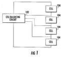
- Fig. 1 is a block diagram illustrating the connection of a cell balancing circuit with a series connection of battery cells
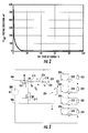
- Fig. 2 illustrates voltage differences between two cells as a function of the percent of state of charge of the cells
- Fig. 3 illustrates a schematic diagram of a circuit for charging and balancing of cells
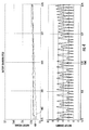
- Fig. 4 illustrates the battery charging cycle during transition
- Fig. 5 illustrates the battery discharging cycle during transition
- Fig. 6 illustrates an alternative embodiment of Fig. 3 ;
- Fig. 7 illustrates yet another embodiment of the circuit of Fig. 3 ;
- Fig. 8 illustrates yet a further alternative embodiment of the circuit of Fig. 3 ;
- Fig. 9 illustrates a further embodiment of the battery charging and balancing circuit
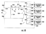
- Fig. 10 illustrates a nested configuration of the charging and balancing circuit
- Fig. 11 is a block diagram of an alternative embodiment of the circuit of Fig. 3 wherein the polarities are reversed on some of the secondary winding portions;
- Fig. 12 illustrates an alternative embodiment including the plurality of series connected transformer portions enabling a stacked configuration that is scalable
- Fig. 13 illustrates yet a further embodiment of a system for reducing the number of transformer secondaries for cell balancing and charging
- Fig. 14 illustrates an alternative embodiment of Fig. 13 wherein diodes are used instead of switches.
- Fig. 15 is a flow diagram describing the operation of the embodiment of Fig. 13 .
- Cell balancing and charging systems provide the ability to charge a series connection of battery cells using a single source.
- Systems using multiple lithium ion or super capacitor cells require balancing of the individual cells in order to maximize the energy available from the batteries and to prolong the life of the system.
- Resistive balancing systems for charging cells dissipate excess charge as heat are one common solution but these types of systems waste energy.
- Energy transfer systems which are based on a "nearest neighbor" inductive or capacitive energy transfer reduce the amount of wasted energy but are complex and generally provide less than satisfactory results when transferring charge over a distance of several cells.
- a cell balancing and charging system that solves the dual problems of balancing the state of charge of cells within a stack of battery cells without dissipating the energy in an associated resistor and further providing efficient transfer of charge to any cell in the stack without a distance penalty.
- the common way of balancing cells within a multi cell battery is by discharging the highest cell through a pass element or alternatively by passing the charge from a pass element to an adjacent cell.
- a cell balancing circuit 102 which is connected with a series connection of battery cells 104.
- the charge level on a particular battery cell 104 may be moved from one cell to another in order to balance the charge load across each of the cells 104.
- the cell balancing circuit 102 is responsible for carrying out this cell balancing/charging functionality.
- Fig. 2 there is illustrated the voltage differences between two cells as a function of the percent state of charge.
- the state of charge of the entire pack is limited.
- the voltage deviation is very high and can approach 500 millivolts deviation.
- the voltage deviation significantly decreases and approaches zero as the state of charge approaches 20%.
- the battery including a higher charge voltage may end up overcharged and damaged, or alternatively, a battery including a lower charge level may end up undercharged in order to protect the higher charge battery. In either case, the battery's cells will not reach their maximum charge voltage.
- the lower charge battery may pull the total capacity of the series connection to a low level and prevent the taking of maximum charge from the system.
- FIG. 3 there is illustrated a first embodiment of a circuit for providing charging and load balancing of a series connection of battery cells 302.
- the series connection of battery cells 302 are connected between node 304 and node 306.
- a charging voltage is supplied to the battery cells 302 via a voltage source 308 provided between nodes 304 and 306.
- Node 306 comprises the ground node while node 304 comprises the input voltage node.
- a high-side switching transistor 310 MOSFET
- MOSFET has its source/drain path connected between node 304 and node 312.
- a low-side switching transistor 314 has its drain/source path connected between node 312 and the ground node 306.
- a resonant tank circuit consisting of inductor 316 and capacitor 320 is connected between node 312 and node 322.
- the inductor 316 is connected between node 312 and node 318.
- the capacitor 320 is connected in series with the inductor 316 between node 318 and node 322.
- a primary side 324 of a transformer 325 is connected to node 322 and to the ground node 306.
- the secondary side of the transformer 325 includes a number of secondary portions 326, each of which are connected across the terminals of an associated battery cell 302. The polarity of adjacent secondary side portions 326 of the transformer are reversed from each other.
- a switching MOSFET 328 has its drain/source path connected between the secondary portion 326 of the transformer 325 and the negative terminal of the associated battery cell 302. The switch 328 would receive control signals from a control circuit (not shown) which also controls switching transistors 310 and 314.
- the system of Fig. 3 is based upon a resonant converter for every switching cycle, and the amount of energy that is put into the resonant tank by the voltage source 308 is then transferred to the secondary side portions 326.
- the lowest charged voltage cells will then take most of the energy transmitted to the secondary side 326 from the resonant tank and the highest charged voltage cells the least.
- the charge is transferred to the second portion 326 in proportion to the charge on the associated battery cells.
- the switch 328 is added in series with each secondary portion 326 to increase or decrease the overall impedance of the battery cell 302. This allows selective charging of the battery cells such as might be required when a cell is to be charged to a higher voltage than other cells. Thus, the cells are balanced during charging.
- waveform 402 represents the charging battery voltage of the lower charge battery cell while waveform 404 represents the higher voltage battery.
- the input to the primary side 324 of the transformer 325 will comprise the total series voltages of all of the battery cells 302.
- the energy is circulating from all of the battery cells 302 back to the lowest charged cells.
- Fig. 5 illustrates the ampere hour taking every cycle from every cell is the same while the energy put back into the system is higher for the lower voltage batteries.
- waveform 502 represents the highest voltage battery cell
- waveform 504 represents the next highest voltage battery cell
- waveform 506 represents the lowest voltage battery cell.
- the main difference between previous solutions and the implementation described herein above with respect to Fig. 3 is that the energy is taken from the entire stack of battery cells 302 and then redistributed back based on the battery cell that needs more energy than the other battery cells.
- This scheme permits very simple systems which automatically distribute charge without the need for a sophisticated control mechanism.
- a more sophisticated implementation is possible in which balancing may be performed using complex algorithms in a manner that maintains optimal performance with a variety of systems over the entire system life.
- the system may be equally implemented as a charger, balancer or both.
- FIG. 6 there is illustrated an alternative implementation of the circuit of Fig. 3 wherein the MOSFET switches 328 between the transformer secondaries 326 and the battery cells 302 are replaced by diodes 602.
- the switches feeding the tank may be removed and the tank input grounded.
- the switches between the transformer secondaries and the cells are replaced by a suitable arrangement of switches and conducting elements.
- Energy is passed to and from the tank circuit by selective use of the secondary side switches.
- the secondary side in figure 2 becomes both primary and secondary depending on the configuration of the switch elements.
- the lower drive MOSFET 314 may be replaced by a diode 802.
- the currents through the transformer primary 324 may be sensed to determine a current limit providing an on time termination point for the circuit and a switch termination timing to determine when to turn off the switching transistors 310 and 314.
- FIG. 9 there is illustrated a further embodiment of the charging/balancing circuit of Fig. 3 .
- the series connection of battery cells 902 are connected between node 904 and node 906.
- a charging voltage is supplied to the battery cells 902 via a voltage source 908 provided between nodes 904 and 906.
- Node 906 comprises the ground node while node 904 comprises the input voltage node.
- a high-side switch 910 is connected between node 904 and node 912.
- a low-side switch 914 is connected between node 912 and the ground node 906.
- a resonant tank circuit consisting of inductor 916 and capacitor 920 is connected between node 912 and node 922.
- the inductor 916 is connected between node 912 and node 918.
- the capacitor 920 is connected in series with the inductor 916 between node 918 and node 922.
- a primary side 924 of a transformer 925 is connected to node 922 and to the ground node 906.
- the secondary side of the transformer 925 includes a number of secondary portions 926, each of which are connected across the terminals of the associated battery cell 902.
- a switch 928 is connected between the secondary portion 926 of the secondary side of the transformer 925 and the negative terminal of the associated battery cell 902.
- the switch 928 would receive control signals from a control circuit (not shown) which also controls switches 915 and 914.
- a capacitor 930 is connected in parallel with the switch 928. In this scheme, current may be directed to individual cells 902 through the selective use of the secondary side switches 928 allowing programmable charge balancing or charge redirection to deliberately produce an unbalanced condition.
- Fig. 10 there is illustrated a nested balancing system. Nested arrangements are possible in which each of the battery cells are replaced by the balancing circuit 1002 as described previously with respect to Fig. 3 and a series of battery cells 1004.
- the circuit of Fig. 10 comprises a series connection of battery cells 1004 are connected between node 1005 and node 1006.
- a charging voltage is supplied to the battery cells 1004 via a voltage source 1008 provided between nodes 1005 and 1006.
- Node 1006 comprises the ground node while node 1005 comprises the input voltage node.
- a high-side switch 1016 is connected between node 1005 and node 1012.
- a low-side switch 1014 is connected between node 1012 and the ground node 1006.
- a resonant tank circuit consisting of inductor 1013 and capacitor 1021 is connected between node 1012 and node 1022.
- the inductor 1013 is connected between node 1012 and node 1018.
- the capacitor 1021 is connected in series with the inductor 1013 between node 1020 and node 1022.
- a primary side 1024 of a transformer 1025 is connected to node 1022 and to the ground node 1006.
- the secondary side of the transformer 1025 includes a number of secondary portions 1026, each of which are connected across the terminals of the associated battery cell stack 1004.
- a switch 1028 is connected between the secondary portion 1026 of the secondary side 1026 of the transformer 1025 and the negative terminal of the associated battery cell stack 1004. The switch 1028 would receive control signals from a circuit which also controls switches 1016 and 1014.
- each stack of cells 1004 includes its own balancing system 1002 such that nested balancing systems may be produced which optimizes the complexity/performance trade off.
- the switches 1016 and 1014 feeding the resonant tank may be removed and the tank input grounded.
- the switches 1028 between the transformer secondaries 1026 and the cell stacks 1004 are replaced by a suitable arrangement of switches and conducting elements. Energy is passed to and from the resonant tank circuit by the selective use of the secondary side switches 1028.
- the secondary side becomes both the primary and secondary depending on the configuration of the switching elements.
- the circuitry is configured in substantially the same manner as that described with respect to Fig. 3 .
- the polarities on the secondary side portions 326 are altered such that some (ideally half) of the secondary windings have one polarity and the remainder of the secondary windings have the opposite polarity.
- the actual sequence between the reversed polarities within the secondary windings is not important.
- the benefit that this configuration provides is that charge may be transferred on both half cycles of the transformer. The first half cycle feeds the secondaries with one polarity and the second half cycle feeds those with the opposite polarity.
- a further embodiment that comprises a stacked configuration including additional transformer 1233 placed in series with the first transformer 1225.
- the series connection of battery cells 1202 are connected between node 1204 and node 1206.
- a charging voltage is supplied to the battery cells 1202 via a voltage source 1208 provided between nodes 1204 and 1206.
- Node 1206 comprises the ground node while node 1204 comprises the input voltage node.
- a high-side switch 1210 is connected between node 1204 and node 1212.
- a low-side switch 1214 is connected between node 1212 and the ground node 1206.
- a resonant tank circuit consisting of inductor 1216 and capacitor 1220 is connected between node 1212 and node 1222.
- the inductor 1216 is connected between node 1212 and node 1218.
- the capacitor 1220 is connected in series with the inductor 1216 between node 1218 and node 1222.
- a primary side 1224 of a first transformer 1225 is connected to node 1222 and to the ground node 1206.
- the secondary side of the transformer 1225 includes a number of secondary portions 1226, each of which are connected across the terminals of the associated battery cell 1202.
- a switch 1228 is connected between the secondary portion of the secondary side 1226 of the transformer 1225 and the negative terminal of the associated battery cell 1202.
- the switch 1228 would receive control signals from a control circuit (not shown) which also controls switches 1215 and 1214.
- a capacitor 1230 is connected in parallel with the switch 1228. In this scheme, current may be directed to individual cells 1202 through the selective use of the secondary side switches 1228 allowing programmable charge balancing or charge redirection to deliberately produce an unbalanced condition.
- a primary side 1235 of the transformer 1223 is connected in series with the primary side 1224 of the first transformer 1225.
- a further series of transformer secondaries 1236 are connected across additional battery cells 1202 in series with the transformer secondary portion 1226 of transformer 1225.
- a switch 1228 would receive control signals from a control circuit (not shown).
- a capacitor 1230 is connected in parallel with the switch 1228.
- the stacked configuration is completely scalable. As many sections as needed may be added in series. Thus, rather than the two illustrated in Fig. 12 , any number may be further added.
- a single pair of switches 1215 and 1214 and a single tank circuit consisting of inductor 1216 and capacitor 1220 then feed the series connected transformer windings.
- FIG. 13 there is illustrated yet a further embodiment of a charge/balancing circuit comprises an improved configuration for reducing the number of transformer secondaries is illustrated.
- a series connection of battery cells 1302 are connected between node 1304 and node 1306.
- a charging voltage is supplied to the battery cells 1302 via a voltage source 1308 provided between nodes 1304 and 1306.
- Node 1306 comprises a ground node while node 1304 comprises the input voltage node.
- a high side switch 1310 is connected between node 1304 and node 1312.
- a low side switch 1314 is connected between node 1312 and the ground node 1306.
- a resonant tank consisting of inductor 1316 and capacitor 1320 is connected between node 1312 and node 1322.
- the inductor 1316 is connected between node 1312 and node 1318.
- the capacitor 1320 is connected in series with the inductor 1316 between node 1318 and node 1322.
- a primary side 1324 of a transformer 1325 is connected to node 1322 and to the ground node 1306.
- the secondary side of the transformer 1325 includes a number of portions 1326. Each secondary portion 1326 is associated with two separate battery cells 1302 via an associated set of switches 1328 and 1330.
- a switch 1328 is connected between a first portion of the secondary side 1326 of the transformer 1325 and a first terminal of an associated battery 1302. The switch 1328 is similarly associated for each secondary portion of the secondary side 1326 within the circuit.
- the switch 1330 is connected between the secondary portion of the secondary side 1326 of the transformer 1325 and a second terminal of a second cell.
- the switch 1330 is associated with each of the secondary portions of the secondary side 1326. The polarities of the secondary side 1326 applied to the battery cells 1302 are reversed during each half cycle application.
- Each portion of the transformer secondary 1326 is connected via switches 1328 and 1330 to two adjacent cells 1302.
- the switches 1328 and 1330 enable a charging current to be transferred to each of the two connected cells 1302 during opposite half cycles of current in the primary winding 1324.
- the secondary winding 1326 is connected via switch 1328 to cells 1302a and 1302c during one half of the duty cycle
- the transformer secondary 1326 is connected to a second group of cells 1302b and 1302d via switches 1330 during the other half of the duty cycle. The sequence will then repeat during each half cycle so that both groups of cells are charged by the actions of the secondary winding 1326.
- FIG. 14 there is illustrated yet a further embodiment of a charge/balancing circuit wherein an alternative configuration for reducing the number of transformer secondaries is illustrated.
- the series connection of battery cells 1402 are connected between node 1404 and node 1406.
- a charging voltage is supplied to the battery cells 1402 via a voltage source 1408 provided between nodes 1404 and 1406.
- Node 1406 comprises a ground node while node 1404 comprises the input voltage node.
- a high side switch 1410 is connected between node 1404 and node 1412.
- a low side switch 1414 is connected between node 1412 and the ground node 1406.
- a resonant tank consisting of inductor 1416 and capacitor 1420 is connected between node 1412 and node 1422.
- the inductor 1416 is connected between node 1412 and node 1418.
- the capacitor 1420 is connected in series with the inductor 1416 between node 1418 and node 1422.
- a primary side 1424 of a transformer 1425 is connected to node 1422 and to the ground node 1406.
- the secondary side of the transformer 1425 includes a number of portions 1426. Each secondary portion 1426 is associated with two separate battery cells 1402 via an associated set of diodes 1428 and 1430.
- a diode 1428 is connected between a first portion of the secondary side 1426 of the transformer 1425 and a first terminal of an associated battery 1402. The diode 1428 is similarly associated for each secondary portion of the secondary side 1426 within the circuit.
- the diode 1430 is connected between the secondary portion of the secondary side 1426 of the transformer 1425 and a second terminal of a second cell.
- the diode 1430 is associated with each of the secondary portions of the secondary side 1426.
- the polarities of the secondary transformer 1426 applied to the battery cells 1402 are reversed during each half cycle application.
- Each portion of the transformer secondary 1426 is connected via diodes 1428 and 1430 to two adjacent cells 1402.
- the diodes 1428 and 1430 enable a charging current to be transferred to each of the two connected cells 1402 during opposite half cycles of current in the primary winding 1424.
- the secondary winding 1426 is connected via diode 1428 to cells 1402a and 1402c during one half of the duty cycle
- the transformer secondary 1426 is connected to a second group of cells 1402b and 1402d via diodes 1430 during the other half of the duty cycle.
- the sequence will then repeat during each half cycle so that both groups of cells are charged by the actions of the secondary winding 1426.
- the switches 1328 and 1330 of the embodiment of Fig. 13 have been replaced by diodes 1428 and 1430.
- the diodes or switches may be replaced by a combination of diodes and switches to permit simple control of the system.
- Fig. 15 there is illustrated a flow diagram describing the operation of the circuit of Fig. 13 .
- the first group of switches 1328 is closed while the second group of switches 1330 is open.
- the first group of batteries is then charged at step 1506.
- Inquiry step 1508 determines if the first half cycle of the current in the primary winding 1324 has been completed. If not, control passes back to step 1506. If inquiry step 1508 determines that the half cycle is completed, the second group of switches 1330 is closed while the first group of switches 1328 is opened at step 1510. This initiates the charging of the second group of batteries at step 1512.
- Inquiry step 1514 determines whether the last half cycle of the current in the primary winding 1326 has been completed and if not, continues charging the battery at step 1512. Once the half cycle is completed, control passes back to step 1504 and the first group of switches are closed while the second group of switches are open to begin charging of the first group of batteries. The cycle continues to repeat as described herein above.
- the energy is taken from the entire cell stack and redistributed based upon the cells that need more energy than the other.
- the scheme permits very simple systems which automatically charge without the need of a sophisticated control mechanism. More sophisticated implementations are possible in which the balancing may be performed using complex algorithms in a manner that maintains the optimal performance with a variety of systems and over the entire system life. Additionally, the above method and systems may be utilized to reduce the number of transformer secondaries within the system by a factor of 2. This will greatly reduce the component costs within the system and provide significant cost savings.
Landscapes
- Engineering & Computer Science (AREA)
- Power Engineering (AREA)
- Manufacturing & Machinery (AREA)
- Chemical & Material Sciences (AREA)
- Chemical Kinetics & Catalysis (AREA)
- Electrochemistry (AREA)
- General Chemical & Material Sciences (AREA)
- Charge And Discharge Circuits For Batteries Or The Like (AREA)
- Secondary Cells (AREA)
Abstract
Description
- This application is a national phase application of
U.S. Patent Application No. 12/779,433, filed May 13, 2010 U.S. Patent Application No. 12/650,775, filed December 31, 2009 U.S. Provisional Patent Application No. 61/180,618, filed May 22, 2009 U.S. Provisional Patent Application No. 61/244,643, filed September 22, 2009 - The present invention relates to self charging systems, and more particularly, to multi-cell balancing or charging systems.
- Cell balancing and charging systems provide the ability to charge a series connection of batteries using a single source. Systems using multiple lithium ion or super capacitor cells require balancing of the individual cells in order to maximize the energy available from the batteries and prolong the life of the system. Resistive balancing systems for charging cells dissipate excess charge as heat in one common solution. However, these types of systems waste a great deal of energy. Energy transfer systems based on a "nearest neighbor" inductive or capacitive energy transfer reduce the amount wasted energy but are complex and generally provide less than satisfactory results when transferring charge over a distance of several cells. Thus, there is a need for a cell balancing and charging system that solves the dual problems of balancing the state of charge of cells within a stack of battery cells without dissipating the energy in an associated resistor, and further providing efficient transfer of charge to any cell in the stack without a distance penalty. The common manner of balancing cells within a multi-cell battery is by discharging the highest cell through a pass element or, alternatively, by passing the charge from a pass element to an adjacent cell.
- The present invention, as disclosed and described herein, in one aspect thereof, comprises an apparatus for charging a plurality of series connected battery cells. First and second input terminals provide a charging voltage to the plurality of series connected battery cells. A transformer includes a primary side associated with the charging voltage and a secondary side including a plurality of portions. Each of the plurality of portions are connected across one of a plurality of series connected battery cells. A switch in series between each of the plurality of portions of the secondary side and the at least one of the series connected battery cells increases an impedance between the portion of the secondary side and the at least one of the plurality of series connected battery cells in a first state and decreases the impedance between the portion of the secondary side and the at least one of the plurality of series connected battery cells in a second state.
- For a more complete understanding, reference is now made to the following description taken in conjunction with the accompanying Drawings in which:
-
Fig. 1 is a block diagram illustrating the connection of a cell balancing circuit with a series connection of battery cells; -
Fig. 2 illustrates voltage differences between two cells as a function of the percent of state of charge of the cells; -
Fig. 3 illustrates a schematic diagram of a circuit for charging and balancing of cells; -
Fig. 4 illustrates the battery charging cycle during transition; -
Fig. 5 illustrates the battery discharging cycle during transition; -
Fig. 6 illustrates an alternative embodiment ofFig. 3 ; -
Fig. 7 illustrates yet another embodiment of the circuit ofFig. 3 ; -
Fig. 8 illustrates yet a further alternative embodiment of the circuit ofFig. 3 ; -
Fig. 9 illustrates a further embodiment of the battery charging and balancing circuit; -
Fig. 10 illustrates a nested configuration of the charging and balancing circuit; -
Fig. 11 is a block diagram of an alternative embodiment of the circuit ofFig. 3 wherein the polarities are reversed on some of the secondary winding portions; -
Fig. 12 illustrates an alternative embodiment including the plurality of series connected transformer portions enabling a stacked configuration that is scalable; -
Fig. 13 illustrates yet a further embodiment of a system for reducing the number of transformer secondaries for cell balancing and charging; -
Fig. 14 illustrates an alternative embodiment ofFig. 13 wherein diodes are used instead of switches; and -
Fig. 15 is a flow diagram describing the operation of the embodiment ofFig. 13 . - [00010] Referring now to the drawings, wherein like reference numbers are used herein to designate like elements throughout, the various views and embodiments of a system and method for cell balancing and charging are illustrated and described, and other possible embodiments are described. The figures are not necessarily drawn to scale, and in some instances the drawings have been exaggerated and/or simplified in places for illustrative purposes only. One of ordinary skill in the art will appreciate the many possible applications and variations based on the following examples of possible embodiments.
- [00011] Cell balancing and charging systems provide the ability to charge a series connection of battery cells using a single source. Systems using multiple lithium ion or super capacitor cells require balancing of the individual cells in order to maximize the energy available from the batteries and to prolong the life of the system. Resistive balancing systems for charging cells dissipate excess charge as heat are one common solution but these types of systems waste energy. Energy transfer systems which are based on a "nearest neighbor" inductive or capacitive energy transfer reduce the amount of wasted energy but are complex and generally provide less than satisfactory results when transferring charge over a distance of several cells. Thus, there is a need for a cell balancing and charging system that solves the dual problems of balancing the state of charge of cells within a stack of battery cells without dissipating the energy in an associated resistor and further providing efficient transfer of charge to any cell in the stack without a distance penalty. The common way of balancing cells within a multi cell battery is by discharging the highest cell through a pass element or alternatively by passing the charge from a pass element to an adjacent cell.
- [00012] Referring now to the drawings, and more particularly to
Fig. 1 , there is illustrated a configuration of acell balancing circuit 102 which is connected with a series connection ofbattery cells 104. The charge level on aparticular battery cell 104 may be moved from one cell to another in order to balance the charge load across each of thecells 104. Thecell balancing circuit 102 is responsible for carrying out this cell balancing/charging functionality. Various types of systems, as discussed herein above, exist for transferring the charge from one cell within a cell stack to an adjacent cell. However, these systems are overly complex and expensive and suffer from poor efficiency when transferring charge over several cells such as from one end of the cell stack to the other. - [00013] Referring now to
Fig. 2 , there is illustrated the voltage differences between two cells as a function of the percent state of charge. When batteries of different impedances or voltages are connected in series, the state of charge of the entire pack is limited. At a low state of charge percentage the voltage deviation is very high and can approach 500 millivolts deviation. The voltage deviation significantly decreases and approaches zero as the state of charge approaches 20%. Thus, during the charging cycle, the battery including a higher charge voltage may end up overcharged and damaged, or alternatively, a battery including a lower charge level may end up undercharged in order to protect the higher charge battery. In either case, the battery's cells will not reach their maximum charge voltage. During discharge, the lower charge battery may pull the total capacity of the series connection to a low level and prevent the taking of maximum charge from the system. - [00014] Referring now to
Fig. 3 , there is illustrated a first embodiment of a circuit for providing charging and load balancing of a series connection ofbattery cells 302. The series connection ofbattery cells 302 are connected betweennode 304 andnode 306. A charging voltage is supplied to thebattery cells 302 via avoltage source 308 provided betweennodes Node 306 comprises the ground node whilenode 304 comprises the input voltage node. A high-side switching transistor 310 (MOSFET) has its source/drain path connected betweennode 304 andnode 312. A low-side switching transistor 314 (MOSFET) has its drain/source path connected betweennode 312 and theground node 306. - A resonant tank circuit consisting of
inductor 316 andcapacitor 320 is connected betweennode 312 andnode 322. Theinductor 316 is connected betweennode 312 andnode 318. Thecapacitor 320 is connected in series with theinductor 316 betweennode 318 andnode 322. Aprimary side 324 of atransformer 325 is connected tonode 322 and to theground node 306. The secondary side of thetransformer 325 includes a number ofsecondary portions 326, each of which are connected across the terminals of an associatedbattery cell 302. The polarity of adjacentsecondary side portions 326 of the transformer are reversed from each other. A switchingMOSFET 328 has its drain/source path connected between thesecondary portion 326 of thetransformer 325 and the negative terminal of the associatedbattery cell 302. Theswitch 328 would receive control signals from a control circuit (not shown) which also controls switchingtransistors - During the charging cycle, the system of
Fig. 3 is based upon a resonant converter for every switching cycle, and the amount of energy that is put into the resonant tank by thevoltage source 308 is then transferred to thesecondary side portions 326. The lowest charged voltage cells will then take most of the energy transmitted to thesecondary side 326 from the resonant tank and the highest charged voltage cells the least. Thus, the charge is transferred to thesecond portion 326 in proportion to the charge on the associated battery cells. In order to add more protection and control, theswitch 328 is added in series with eachsecondary portion 326 to increase or decrease the overall impedance of thebattery cell 302. This allows selective charging of the battery cells such as might be required when a cell is to be charged to a higher voltage than other cells. Thus, the cells are balanced during charging. - As can be seen in
Fig. 4 , the lowest voltage cells are taking all of the energy provided by the resonant tank while the higher voltage battery cells are sitting idle until the lower battery cells catch up in charge value with the higher value tanks. Thus,waveform 402 represents the charging battery voltage of the lower charge battery cell whilewaveform 404 represents the higher voltage battery. - During the discharge cycle, the input to the
primary side 324 of thetransformer 325 will comprise the total series voltages of all of thebattery cells 302. The energy is circulating from all of thebattery cells 302 back to the lowest charged cells.Fig. 5 illustrates the ampere hour taking every cycle from every cell is the same while the energy put back into the system is higher for the lower voltage batteries. Thus,waveform 502 represents the highest voltage battery cell,waveform 504 represents the next highest voltage battery cell whilewaveform 506 represents the lowest voltage battery cell. - The main difference between previous solutions and the implementation described herein above with respect to
Fig. 3 , is that the energy is taken from the entire stack ofbattery cells 302 and then redistributed back based on the battery cell that needs more energy than the other battery cells. This scheme permits very simple systems which automatically distribute charge without the need for a sophisticated control mechanism. A more sophisticated implementation is possible in which balancing may be performed using complex algorithms in a manner that maintains optimal performance with a variety of systems over the entire system life. The system may be equally implemented as a charger, balancer or both. - Referring now to
Fig. 6 , there is illustrated an alternative implementation of the circuit ofFig. 3 wherein the MOSFET switches 328 between thetransformer secondaries 326 and thebattery cells 302 are replaced by diodes 602. In another implementation illustrated inFig. 7 , the switches feeding the tank may be removed and the tank input grounded. In this system the switches between the transformer secondaries and the cells are replaced by a suitable arrangement of switches and conducting elements. Energy is passed to and from the tank circuit by selective use of the secondary side switches. E.g. the secondary side infigure 2 becomes both primary and secondary depending on the configuration of the switch elements. Alternatively, as illustrated inFig. 8 , thelower drive MOSFET 314 may be replaced by a diode 802. In an alternative control scheme, the currents through thetransformer primary 324 may be sensed to determine a current limit providing an on time termination point for the circuit and a switch termination timing to determine when to turn off the switchingtransistors - Referring now to
Fig. 9 , there is illustrated a further embodiment of the charging/balancing circuit ofFig. 3 . The series connection ofbattery cells 902 are connected betweennode 904 andnode 906. A charging voltage is supplied to thebattery cells 902 via avoltage source 908 provided betweennodes Node 906 comprises the ground node whilenode 904 comprises the input voltage node. A high-side switch 910 is connected betweennode 904 andnode 912. A low-side switch 914 is connected betweennode 912 and theground node 906. A resonant tank circuit consisting ofinductor 916 andcapacitor 920 is connected betweennode 912 andnode 922. Theinductor 916 is connected betweennode 912 andnode 918. Thecapacitor 920 is connected in series with theinductor 916 betweennode 918 andnode 922. - A
primary side 924 of atransformer 925 is connected tonode 922 and to theground node 906. The secondary side of thetransformer 925 includes a number ofsecondary portions 926, each of which are connected across the terminals of the associatedbattery cell 902. Aswitch 928 is connected between thesecondary portion 926 of the secondary side of thetransformer 925 and the negative terminal of the associatedbattery cell 902. Theswitch 928 would receive control signals from a control circuit (not shown) which also controlsswitches switch 928 connected between the transformersecondary portion 926 and thebattery cell 902, acapacitor 930 is connected in parallel with theswitch 928. In this scheme, current may be directed toindividual cells 902 through the selective use of the secondary side switches 928 allowing programmable charge balancing or charge redirection to deliberately produce an unbalanced condition. - Referring now also to
Fig. 10 , there is illustrated a nested balancing system. Nested arrangements are possible in which each of the battery cells are replaced by thebalancing circuit 1002 as described previously with respect toFig. 3 and a series ofbattery cells 1004. The circuit ofFig. 10 comprises a series connection ofbattery cells 1004 are connected betweennode 1005 andnode 1006. A charging voltage is supplied to thebattery cells 1004 via avoltage source 1008 provided betweennodes Node 1006 comprises the ground node whilenode 1005 comprises the input voltage node. A high-side switch 1016 is connected betweennode 1005 andnode 1012. A low-side switch 1014 is connected betweennode 1012 and theground node 1006. - A resonant tank circuit consisting of
inductor 1013 andcapacitor 1021 is connected betweennode 1012 andnode 1022. Theinductor 1013 is connected betweennode 1012 and node 1018. Thecapacitor 1021 is connected in series with theinductor 1013 betweennode 1020 andnode 1022. Aprimary side 1024 of atransformer 1025 is connected tonode 1022 and to theground node 1006. The secondary side of thetransformer 1025 includes a number ofsecondary portions 1026, each of which are connected across the terminals of the associatedbattery cell stack 1004. Aswitch 1028 is connected between thesecondary portion 1026 of thesecondary side 1026 of thetransformer 1025 and the negative terminal of the associatedbattery cell stack 1004. Theswitch 1028 would receive control signals from a circuit which also controlsswitches - As mentioned previously, rather than a single cell, a series of
cells 1004 are connected across each of thesecondary portions 1026 of the secondary side of the transformer. Connected across thesecells 1004 is the balancing circuit described previously with respect toFig. 3 . Thus, thebattery cells 1004 would comprise thesource 308 and thebalancing circuit 1002 would connect with the source atnodes cells 1004 includes itsown balancing system 1002 such that nested balancing systems may be produced which optimizes the complexity/performance trade off. - In an alternative embodiment of the circuit of
Fig. 10 , theswitches switches 1028 between thetransformer secondaries 1026 and thecell stacks 1004 are replaced by a suitable arrangement of switches and conducting elements. Energy is passed to and from the resonant tank circuit by the selective use of the secondary side switches 1028. Thus, the secondary side becomes both the primary and secondary depending on the configuration of the switching elements. - In yet a further embodiment illustrated in
Fig. 11 , the circuitry is configured in substantially the same manner as that described with respect toFig. 3 . However, the polarities on thesecondary side portions 326 are altered such that some (ideally half) of the secondary windings have one polarity and the remainder of the secondary windings have the opposite polarity. The actual sequence between the reversed polarities within the secondary windings is not important. The benefit that this configuration provides is that charge may be transferred on both half cycles of the transformer. The first half cycle feeds the secondaries with one polarity and the second half cycle feeds those with the opposite polarity. - Referring now to
Fig. 12 , there is illustrated a further embodiment that comprises a stacked configuration includingadditional transformer 1233 placed in series with thefirst transformer 1225. The series connection ofbattery cells 1202 are connected betweennode 1204 andnode 1206. A charging voltage is supplied to thebattery cells 1202 via avoltage source 1208 provided betweennodes Node 1206 comprises the ground node whilenode 1204 comprises the input voltage node. A high-side switch 1210 is connected betweennode 1204 andnode 1212. A low-side switch 1214 is connected betweennode 1212 and theground node 1206. A resonant tank circuit consisting ofinductor 1216 andcapacitor 1220 is connected betweennode 1212 and node 1222. Theinductor 1216 is connected betweennode 1212 and node 1218. Thecapacitor 1220 is connected in series with theinductor 1216 between node 1218 and node 1222. - A
primary side 1224 of afirst transformer 1225 is connected to node 1222 and to theground node 1206. The secondary side of thetransformer 1225 includes a number ofsecondary portions 1226, each of which are connected across the terminals of the associatedbattery cell 1202. Aswitch 1228 is connected between the secondary portion of thesecondary side 1226 of thetransformer 1225 and the negative terminal of the associatedbattery cell 1202. Theswitch 1228 would receive control signals from a control circuit (not shown) which also controlsswitches switch 1228 connected between the transformersecondary portion 1226 and thebattery cell 1202, acapacitor 1230 is connected in parallel with theswitch 1228. In this scheme, current may be directed toindividual cells 1202 through the selective use of thesecondary side switches 1228 allowing programmable charge balancing or charge redirection to deliberately produce an unbalanced condition. - In the
second transformer 1223 of the stacked configuration, aprimary side 1235 of thetransformer 1223 is connected in series with theprimary side 1224 of thefirst transformer 1225. Additionally, a further series oftransformer secondaries 1236 are connected acrossadditional battery cells 1202 in series with the transformersecondary portion 1226 oftransformer 1225. As in the first portion of the circuit, aswitch 1228 would receive control signals from a control circuit (not shown). In addition to theswitch 1228 connected between the transformersecondary portion 1236 and thebattery cell 1202, acapacitor 1230 is connected in parallel with theswitch 1228. The stacked configuration is completely scalable. As many sections as needed may be added in series. Thus, rather than the two illustrated inFig. 12 , any number may be further added. A single pair ofswitches inductor 1216 andcapacitor 1220 then feed the series connected transformer windings. - Referring now to
Fig. 13 , there is illustrated yet a further embodiment of a charge/balancing circuit comprises an improved configuration for reducing the number of transformer secondaries is illustrated. A series connection of battery cells 1302 are connected betweennode 1304 andnode 1306. A charging voltage is supplied to the battery cells 1302 via avoltage source 1308 provided betweennodes Node 1306 comprises a ground node whilenode 1304 comprises the input voltage node. Ahigh side switch 1310 is connected betweennode 1304 andnode 1312. Alow side switch 1314 is connected betweennode 1312 and theground node 1306. A resonant tank consisting ofinductor 1316 andcapacitor 1320 is connected betweennode 1312 andnode 1322. Theinductor 1316 is connected betweennode 1312 andnode 1318. Thecapacitor 1320 is connected in series with theinductor 1316 betweennode 1318 andnode 1322. - A
primary side 1324 of atransformer 1325 is connected tonode 1322 and to theground node 1306. The secondary side of thetransformer 1325 includes a number ofportions 1326. Eachsecondary portion 1326 is associated with two separate battery cells 1302 via an associated set ofswitches switch 1328 is connected between a first portion of thesecondary side 1326 of thetransformer 1325 and a first terminal of an associated battery 1302. Theswitch 1328 is similarly associated for each secondary portion of thesecondary side 1326 within the circuit. Similarly, theswitch 1330 is connected between the secondary portion of thesecondary side 1326 of thetransformer 1325 and a second terminal of a second cell. Theswitch 1330 is associated with each of the secondary portions of thesecondary side 1326. The polarities of thesecondary side 1326 applied to the battery cells 1302 are reversed during each half cycle application. - Each portion of the transformer secondary 1326 is connected via
switches switches switch 1328 tocells cells switches 1330 during the other half of the duty cycle. The sequence will then repeat during each half cycle so that both groups of cells are charged by the actions of the secondary winding 1326. - Referring now to
Fig. 14 , there is illustrated yet a further embodiment of a charge/balancing circuit wherein an alternative configuration for reducing the number of transformer secondaries is illustrated. The series connection of battery cells 1402 are connected betweennode 1404 andnode 1406. A charging voltage is supplied to the battery cells 1402 via avoltage source 1408 provided betweennodes Node 1406 comprises a ground node whilenode 1404 comprises the input voltage node. Ahigh side switch 1410 is connected betweennode 1404 andnode 1412. Alow side switch 1414 is connected betweennode 1412 and theground node 1406. A resonant tank consisting ofinductor 1416 andcapacitor 1420 is connected betweennode 1412 andnode 1422. Theinductor 1416 is connected betweennode 1412 andnode 1418. Thecapacitor 1420 is connected in series with theinductor 1416 betweennode 1418 andnode 1422. - A
primary side 1424 of atransformer 1425 is connected tonode 1422 and to theground node 1406. The secondary side of thetransformer 1425 includes a number ofportions 1426. Eachsecondary portion 1426 is associated with two separate battery cells 1402 via an associated set ofdiodes diode 1428 is connected between a first portion of thesecondary side 1426 of thetransformer 1425 and a first terminal of an associated battery 1402. Thediode 1428 is similarly associated for each secondary portion of thesecondary side 1426 within the circuit. Similarly, thediode 1430 is connected between the secondary portion of thesecondary side 1426 of thetransformer 1425 and a second terminal of a second cell. Thediode 1430 is associated with each of the secondary portions of thesecondary side 1426. The polarities of thesecondary transformer 1426 applied to the battery cells 1402 are reversed during each half cycle application. - Each portion of the transformer secondary 1426 is connected via
diodes diodes diode 1428 tocells cells diodes 1430 during the other half of the duty cycle. The sequence will then repeat during each half cycle so that both groups of cells are charged by the actions of the secondary winding 1426. In the implementation ofFig. 14 , theswitches Fig. 13 have been replaced bydiodes - Referring now to
Fig. 15 , there is illustrated a flow diagram describing the operation of the circuit ofFig. 13 . Once the operation of the circuit is initiated atstep 1502, the first group ofswitches 1328 is closed while the second group ofswitches 1330 is open. When this occurs, the first group of batteries is then charged atstep 1506.Inquiry step 1508 determines if the first half cycle of the current in the primary winding 1324 has been completed. If not, control passes back tostep 1506. Ifinquiry step 1508 determines that the half cycle is completed, the second group ofswitches 1330 is closed while the first group ofswitches 1328 is opened atstep 1510. This initiates the charging of the second group of batteries atstep 1512.Inquiry step 1514 then determines whether the last half cycle of the current in the primary winding 1326 has been completed and if not, continues charging the battery atstep 1512. Once the half cycle is completed, control passes back tostep 1504 and the first group of switches are closed while the second group of switches are open to begin charging of the first group of batteries. The cycle continues to repeat as described herein above. - Thus, the main difference between previous solutions and the present disclosure is that the energy is taken from the entire cell stack and redistributed based upon the cells that need more energy than the other. The scheme permits very simple systems which automatically charge without the need of a sophisticated control mechanism. More sophisticated implementations are possible in which the balancing may be performed using complex algorithms in a manner that maintains the optimal performance with a variety of systems and over the entire system life. Additionally, the above method and systems may be utilized to reduce the number of transformer secondaries within the system by a factor of 2. This will greatly reduce the component costs within the system and provide significant cost savings.
- It will be appreciated by those skilled in the art having the benefit of this disclosure that this system and method for cell balancing and charging provides an improved manner of charging/balancing a stack of battery cells. It should be understood that the drawings and detailed description herein are to be regarded in an illustrative rather than a restrictive manner, and are not intended to be limiting to the particular forms and examples disclosed. On the contrary, included are any further modifications, changes, rearrangements, substitutions, alternatives, design choices, and embodiments apparent to those of ordinary skill in the art, without departing from the spirit and scope hereof, as defined by the following claims. Thus, it is intended that the following claims be interpreted to embrace all such further modifications, changes, rearrangements, substitutions, alternatives, design choices, and embodiments.
Claims (31)
- An apparatus for charging a plurality of series connected battery cells, comprising:first and second input terminals for providing a charging voltage to the plurality of series connected battery cells;a transformer including a primary side associated with the charging voltage and a secondary side including a plurality of portions, each of the plurality of portions connected across at least two of the plurality of series connected battery cells;a first switch in series between each of the plurality of portions of the secondary side and a first battery cell of the at least two of the plurality of series connected battery cells for providing a charging current to the first battery cell during a first portion of a cycle of a current in the primary side of the transformer; anda second switch in series between each of the plurality of portions of the secondary side and a second battery cell of the at least two of the plurality of series connected battery cells for providing a charging current to the second battery cell during a second portion of the cycle of the current in the primary side of the transformer.
- The apparatus of Claim 1, wherein in a charging mode charge on the primary side is transferred to the plurality of portions of the secondary side, the voltage from the primary side divided amongst the plurality of portions of the secondary side in proportion to an amount of charge needed by the first or second battery cell associated with the portion of the secondary side and in a discharging mode an input to the primary side of the transformer comprises a total series voltage of the plurality of series connected battery cells.
- The apparatus of Claim 1, further including a resonant circuit connected between the primary side of the transformer and the first and second input terminals.
- The apparatus of Claim 3, further including a switching circuit, the switching circuit comprising:a first switch connected between the first input terminal and the resonant circuit; anda second switch connected between the second input terminal and the resonant circuit.
- The apparatus of Claim 3, further including:a first diode connected between the first input terminal and the resonant circuit; anda second diode connected between the second input terminal and the resonant circuit.
- The apparatus of Claim 1, wherein the first switch and the second switch comprise a MOSFET transistor.
- The apparatus of Claim 1, wherein each of the plurality of portions of the secondary sides are connected with a first polarity across the first battery cell and with a second polarity across the second battery cell.
- The apparatus of Claim 1, further including a diode associated with the first switch and the second switch for providing a charging current to the first battery cell and the second battery cell.
- An apparatus for charging a plurality of series connected battery cells, comprising:first and second input terminals for providing a charging voltage to the plurality of series connected battery cells;a transformer including a primary side associated with the charging voltage and a secondary side including a plurality of portions, each of the plurality of portions connected across at least two of the plurality of series connected battery cells;a first diode in series between each of the plurality of portions of the secondary side and a first battery cell of the at least two of the plurality of series connected battery cells for providing a charging current to the first battery cell during a first portion of a cycle of a current in the primary side of the transformer; anda second diode in series between each of the plurality of portions of the secondary side and a second battery cell of the at least two of the plurality of series connected battery cells for providing a charging current to the to the second battery cell during a second portion of the cycle of the current in the primary side of the transformer.
- The apparatus of Claim 9, wherein in a charging mode charge on the primary side is transferred to the plurality of portions of the secondary side, the voltage from the primary side divided amongst the plurality of portions of the secondary side in proportion to an amount of charge needed by the first or second battery cell associated with the portion of the secondary side and in a discharging mode an input to the primary side of the transformer comprises a total series voltage of the plurality of series connected battery cells.
- The apparatus of Claim 9, further including a resonant circuit connected between the primary side of the transformer and the first and second input terminals.
- The apparatus of Claim 11, further including a switching circuit, the switching circuit comprising:a first switch connected between the first input terminal and the resonant circuit; anda second switch connected between the second input terminal and the resonant circuit.
- The apparatus of Claim 11, further including:a first diode connected between the first input terminal and the resonant circuit; anda second diode connected between the second input terminal and the resonant circuit.
- The apparatus of Claim 9, wherein each of the plurality of portions of the secondary sides are connected with a first polarity across the first battery cell and with a second polarity across the second battery cell.
- An apparatus for charging a plurality of series connected battery cells, comprising:first and second input terminals for providing a charging voltage to the plurality of series connected battery cells;a transformer including a primary side associated with the charging voltage and a secondary side including a plurality of portions, each of the plurality of portions connected across at least one of the plurality of series connected battery cells; anda switch in series between each of the plurality of portions of the secondary side and the at least one of the plurality of series connected battery cells for increasing an impedance between the portion of the secondary side and the at least one of the plurality of series connected battery cells in a first state and for decreasing the impedance between the portion of the secondary side and the at least one of the plurality of series connected battery cells in a second state.
- The apparatus of Claim 15, wherein in a charging mode charge on the primary side is transferred to the plurality of portions of the secondary side, the voltage from the primary side divided amongst the plurality of portions of the secondary side in proportion to an amount of charge needed by the at least one battery cell associated with the portion of the secondary side and in a discharging mode an input to the primary side of the transformer comprises a total series voltage of the plurality of series connected battery cells.
- The apparatus of Claim 15, further including a resonant circuit connected between the primary side of the transformer and the first and second input terminals.
- The apparatus of Claim 17, further including switching circuit, the switching circuit comprising:a first switch connected between the first input terminal and the resonant circuit; anda second switch connected between the second input terminal and the resonant circuit.
- The apparatus of Claim 17, further including:a first diode connected between the first input terminal and the resonant circuit; anda second diode connected between the second input terminal and the resonant circuit.
- The apparatus of Claim 15, wherein the switch comprises a MOSFET transistor.
- The apparatus of Claim 15, further comprising a capacitor in parallel with the switch in series between each of the plurality of portions of the secondary side and the at least one of the plurality of series connected battery cells.
- The apparatus of Claim 15, further comprising:wherein each of the at least one of the plurality of series connected battery cells comprises a second plurality of series connected battery cells;second and third input terminals for providing a second charging voltage to the second plurality of series connected battery cells;a second transformer including a second primary side associated with the second charging voltage and a second secondary side including a second plurality of portions, each of the second plurality of portions connected across an associated battery cell of the second plurality of series connected battery cells; anda second switch in series between each of the second plurality of portions of the secondary side and the associated battery cell for increasing an impedance between the second portion of the secondary side and the battery cell in a first state and for decreasing the impedance between the second portion of the secondary side and the associated battery cell in a second state.
- An apparatus for charging a plurality of series connected battery cells, comprising:first and second input terminals for providing a charging voltage to the plurality of series connected battery cells;a transformer including a primary side associated with the charging voltage and a secondary side including a plurality of portions, each of the plurality of portions connected across at least one of the plurality of series connected battery cells;a resonant circuit connected between the primary side of the transformer and the first and second input terminals;a switch in series between each of the plurality of portions of the secondary side and the at least one of the plurality of series connected battery cells for increasing an impedance between the portion of the secondary side and the at least one of the plurality of series connected battery cells in a first state and for decreasing the impedance between the portion of the secondary side and the at least one of the plurality of series connected battery cells in a second state; andwherein in a charging mode charge on the primary side is transferred to the plurality of portions of the secondary side, the voltage from the primary side divided amongst the plurality of portions of the secondary side in proportion to an amount of charge needed by the at least one battery cell associated with the portion of the secondary side and in a discharging mode an input to the primary side of the transformer comprises a total series voltage of the plurality of series connected battery cells.
- The apparatus of Claim 23, further including switching circuit, the switching circuit comprising:a first switch connected between the first input terminal and the resonant circuit; anda second switch connected between the second input terminal and the resonant circuit.
- The apparatus of Claim 23, further including:a first diode connected between the first input terminal and the resonant circuit; anda second diode connected between the second input terminal and the resonant circuit.
- The apparatus of Claim 23, wherein the switch comprises a MOSFET transistor.
- The apparatus of Claim 23, further comprising a capacitor in parallel with the switch in series between each of the plurality of portions of the secondary side and the at least one of the plurality of series connected battery cells.
- The apparatus of Claim 23, further comprising:wherein each of the at least one of the plurality of series connected battery cells comprises a second plurality of series connected battery cells;second and third input terminals for providing a second charging voltage to the second plurality of series connected battery cells;a second transformer including a second primary side associated with the second charging voltage and a second secondary side including a second plurality of portions, each of the second plurality of portions connected across an associated battery cell of the second plurality of series connected battery cells; anda second switch in series between each of the second plurality of portions of the secondary side and the associated battery cell for increasing an impedance between the second portion of the secondary side and the battery cell in a first state and for decreasing the impedance between the second portion of the secondary side and the associated battery cell in a second state.
- A method for charging a plurality of series connected battery cells, comprising the steps of:receiving a charging voltage for the plurality of series connected battery cells;transferring from a primary side of a transformer to a plurality of portions of a secondary side in a charging mode;dividing the voltage from the primary side amongst the plurality of portions of the secondary side in proportion to an amount of charge needed by at least one battery cell associated with the portion of the secondary side;transferring a total series voltage of the plurality of series connected battery cells to the primary side of the transformer in a discharging mode;increasing an impedance between the portion of the secondary side and the at least one of the plurality of series connected battery cells in a first state; anddecreasing the impedance between the portion of the secondary side and the at least one of the plurality of series connected battery cells in a second state.
- The method of Claim 29, further including the step of generating a resonant input to the primary side of the transformer responsive to the charging voltage.
- The method of Claim 30, further including step of switching the charging voltage to a resonant circuit providing the resonant input.
Priority Applications (2)
| Application Number | Priority Date | Filing Date | Title |
|---|---|---|---|
| EP15202503.7A EP3026783B1 (en) | 2009-05-22 | 2010-05-21 | System and method for cell balancing and charging using a serially coupled inductor and capacitor |
| EP15202520.1A EP3029801B1 (en) | 2009-05-22 | 2010-05-21 | System and method for cell balancing and charging using a serially coupled inductor and capacitor |
Applications Claiming Priority (4)
| Application Number | Priority Date | Filing Date | Title |
|---|---|---|---|
| US18061809P | 2009-05-22 | 2009-05-22 | |
| US24464309P | 2009-09-22 | 2009-09-22 | |
| US12/650,775 US9397508B2 (en) | 2009-05-22 | 2009-12-31 | System and method for cell balancing and charging using a serially coupled inductor and capacitor |
| US12/779,433 US8541980B2 (en) | 2009-05-22 | 2010-05-13 | System and method for cell balancing and charging |
Related Child Applications (4)
| Application Number | Title | Priority Date | Filing Date |
|---|---|---|---|
| EP15202520.1A Division EP3029801B1 (en) | 2009-05-22 | 2010-05-21 | System and method for cell balancing and charging using a serially coupled inductor and capacitor |
| EP15202520.1A Division-Into EP3029801B1 (en) | 2009-05-22 | 2010-05-21 | System and method for cell balancing and charging using a serially coupled inductor and capacitor |
| EP15202503.7A Division EP3026783B1 (en) | 2009-05-22 | 2010-05-21 | System and method for cell balancing and charging using a serially coupled inductor and capacitor |
| EP15202503.7A Division-Into EP3026783B1 (en) | 2009-05-22 | 2010-05-21 | System and method for cell balancing and charging using a serially coupled inductor and capacitor |
Publications (3)
| Publication Number | Publication Date |
|---|---|
| EP2276140A2 true EP2276140A2 (en) | 2011-01-19 |
| EP2276140A3 EP2276140A3 (en) | 2013-12-04 |
| EP2276140B1 EP2276140B1 (en) | 2020-07-15 |
Family
ID=43124160
Family Applications (3)
| Application Number | Title | Priority Date | Filing Date |
|---|---|---|---|
| EP15202520.1A Active EP3029801B1 (en) | 2009-05-22 | 2010-05-21 | System and method for cell balancing and charging using a serially coupled inductor and capacitor |
| EP15202503.7A Active EP3026783B1 (en) | 2009-05-22 | 2010-05-21 | System and method for cell balancing and charging using a serially coupled inductor and capacitor |
| EP10163571.2A Active EP2276140B1 (en) | 2009-05-22 | 2010-05-21 | System and method for cell balancing and charging |
Family Applications Before (2)
| Application Number | Title | Priority Date | Filing Date |
|---|---|---|---|
| EP15202520.1A Active EP3029801B1 (en) | 2009-05-22 | 2010-05-21 | System and method for cell balancing and charging using a serially coupled inductor and capacitor |
| EP15202503.7A Active EP3026783B1 (en) | 2009-05-22 | 2010-05-21 | System and method for cell balancing and charging using a serially coupled inductor and capacitor |
Country Status (6)
| Country | Link |
|---|---|
| US (1) | US8541980B2 (en) |
| EP (3) | EP3029801B1 (en) |
| JP (1) | JP5641781B2 (en) |
| KR (5) | KR20100126235A (en) |
| CN (3) | CN106356923A (en) |
| TW (1) | TWI483507B (en) |
Cited By (4)
| Publication number | Priority date | Publication date | Assignee | Title |
|---|---|---|---|---|
| EP2843796A1 (en) * | 2013-08-27 | 2015-03-04 | General Electric Company | Battery management system and method |
| WO2015079188A1 (en) * | 2013-11-29 | 2015-06-04 | Commissariat à l'énergie atomique et aux énergies alternatives | Device for balancing a power battery element load |
| US10008861B2 (en) | 2012-05-15 | 2018-06-26 | Renault S.A.S. | Charge balancing in a battery |
| US10164441B2 (en) | 2009-05-22 | 2018-12-25 | Intersil Americas LLC | System and method for cell balancing and charging using a serially coupled inductor and capacitor |
Families Citing this family (38)
| Publication number | Priority date | Publication date | Assignee | Title |
|---|---|---|---|---|
| US8798175B2 (en) | 2009-05-08 | 2014-08-05 | Intersil Americas LLC | Communicating with a self-clocking amplitude modulated signal |
| US8933665B2 (en) | 2009-08-05 | 2015-01-13 | Apple Inc. | Balancing voltages between battery banks |
| DE102010029427A1 (en) * | 2010-05-28 | 2011-12-01 | Siemens Aktiengesellschaft | Energy storage device |
| CN102111003B (en) * | 2011-02-21 | 2013-07-17 | 成都芯源系统有限公司 | Novel battery equalization circuit and adjusting method thereof |
| KR101294378B1 (en) * | 2011-02-22 | 2013-08-23 | 주식회사 에너닉스 | BATTERY BALANCING CONTROL APPARATUS and METHOD THEREOF |
| DE102011015523A1 (en) * | 2011-03-30 | 2012-10-04 | Ads-Tec Gmbh | Circuit arrangement for charge equalization in a battery block arrangement |
| CN103493331B (en) * | 2011-04-19 | 2016-06-08 | 新电元工业株式会社 | Unit balancing circuitry and unit bascule |
| WO2012172468A2 (en) * | 2011-06-11 | 2012-12-20 | Sendyne Corp. | Charge redistribution method for cell arrays |
| DE102011079874A1 (en) * | 2011-07-27 | 2013-01-31 | Robert Bosch Gmbh | Energy storage device, system with energy storage device and method for operating an energy storage device |
| US9203121B2 (en) | 2011-10-12 | 2015-12-01 | Texas Instruments Incorporated | Inductor-based active balancing for batteries and other power supplies |
| DE102011086309A1 (en) * | 2011-11-14 | 2013-05-16 | Continental Automotive Gmbh | Circuit arrangement with counter-phase working charge pumps for charging an electrical energy storage |
| WO2013115947A2 (en) * | 2012-01-30 | 2013-08-08 | Apple Inc. | Balancing voltages between battery banks |
| TW201336200A (en) | 2012-02-16 | 2013-09-01 | 國立成功大學 | Series battery balance charging/discharging circuit and control method thereof |
| TWI452800B (en) * | 2012-02-20 | 2014-09-11 | Univ Nat Changhua Education | Battery charging device and method with battery balance |
| JP2013187930A (en) * | 2012-03-06 | 2013-09-19 | Toyota Industries Corp | Cell balance device |
| KR101397026B1 (en) * | 2012-03-12 | 2014-05-20 | 삼성에스디아이 주식회사 | Battery system and energy storage system including same |
| TWI451657B (en) * | 2012-10-29 | 2014-09-01 | Univ Nat Formosa | Equivalent status detecting and charging device for secondary battery package |
| US8901888B1 (en) | 2013-07-16 | 2014-12-02 | Christopher V. Beckman | Batteries for optimizing output and charge balance with adjustable, exportable and addressable characteristics |
| CN104124726B (en) | 2013-04-25 | 2016-08-31 | 财团法人工业技术研究院 | Charging device and charging method |
| TWI502849B (en) * | 2013-04-25 | 2015-10-01 | Ind Tech Res Inst | Matrix charger apparatus and charging method |
| US9160330B2 (en) | 2013-05-02 | 2015-10-13 | Texas Instruments Incorporated | Boost capacitor sharing architecture for power supply active balancing systems |
| DE102013106872A1 (en) * | 2013-07-01 | 2015-01-08 | H-Tech Ag | Device and method for charge equalization of an energy storage device |
| US9819208B2 (en) * | 2014-08-29 | 2017-11-14 | General Electronics Applications, Inc. | Battery management circuit having cell connections for batteries and a plurality of corresponding windings and diodes |
| KR101649755B1 (en) * | 2014-10-02 | 2016-08-23 | 주식회사 에너닉스 | ACTIVE BALANCING CONTROL CIRCUIT and INFORMATION CALCULATING PROCESSING METHOD THERE OF |
| US20160149421A1 (en) * | 2014-11-24 | 2016-05-26 | Southwest Electronic Energy Corporation | Low voltage charging and balancing of a high voltage, series-connected string of battery modules |
| US10574063B2 (en) * | 2015-07-14 | 2020-02-25 | Volvo Truck Corporation | Method and system for balancing a battery pack |
| TWI610486B (en) | 2015-10-14 | 2018-01-01 | 低碳動能開發股份有限公司 | Active balance charging device |
| CN106602653B (en) * | 2016-12-23 | 2018-12-28 | 山东航天电子技术研究所 | A kind of lithium ion battery non-dissipative equalizing circuit |
| WO2018134827A1 (en) * | 2017-01-23 | 2018-07-26 | B.G. Negev Technologies And Applications Ltd., At Ben-Gurion University | System for balancing a series of cells |
| TWI630402B (en) * | 2017-11-03 | 2018-07-21 | 致茂電子股份有限公司 | Battery testing apparatus and battery testing method |
| US10444295B2 (en) * | 2017-12-20 | 2019-10-15 | National Chung Shan Institute Of Science And Technology | Battery balance management circuit |
| US12308673B2 (en) * | 2019-03-21 | 2025-05-20 | Hefei Gotion High-Tech Power Energy Co., Ltd. | Active equalizer circuit, battery management system, and power supply system |
| CN112688375B (en) * | 2020-12-03 | 2022-12-16 | 华南理工大学 | Balanced output system based on multi-winding transformer |
| CN113872288B (en) * | 2021-09-28 | 2023-07-18 | 傲普(上海)新能源有限公司 | A voltage equalization circuit and method for battery cells in a battery module |
| KR102749309B1 (en) * | 2022-02-21 | 2025-01-02 | 주식회사 모큐라텍 | Battery control system based on active balancing |
| US12401206B2 (en) | 2022-04-21 | 2025-08-26 | Liftwave, Inc. | Battery balancing system |
| WO2024151507A1 (en) * | 2023-01-10 | 2024-07-18 | Texas Instruments Incorporated | Active cell balancing |
| US20240322696A1 (en) * | 2023-03-21 | 2024-09-26 | Sensata Technologies, Inc. | Isolated solid-state active pre-charger |
Family Cites Families (21)
| Publication number | Priority date | Publication date | Assignee | Title |
|---|---|---|---|---|
| US5568036A (en) * | 1994-12-02 | 1996-10-22 | Delco Electronics Corp. | Contactless battery charging system with high voltage cable |
| FR2735624B1 (en) * | 1995-06-16 | 1997-09-05 | Smh Management Services Ag | CHARGER FOR ELECTRIC ENERGY ACCUMULATOR |
| US5747968A (en) * | 1996-01-11 | 1998-05-05 | Lockheed Martin Corp. Missiles & Space | Lithium polymer battery charger apparatus |
| US5793624A (en) * | 1996-06-05 | 1998-08-11 | Hydro-Quebec | Apparatus and method for charging a DC battery |
| US5982143A (en) * | 1996-08-27 | 1999-11-09 | The University Of Toledo | Battery equalization circuit with ramp converter and selective outputs |
| US6140800A (en) * | 1999-05-27 | 2000-10-31 | Peterson; William Anders | Autonomous battery equalization circuit |
| TW542470U (en) * | 2000-07-11 | 2003-07-11 | Ind Tech Res Inst | Battery voltage balancer |
| US6642693B2 (en) * | 2000-11-21 | 2003-11-04 | Nagano Japan Radio Co., Ltd. | Voltage equalizing apparatus for battery devices |
| US20040217735A1 (en) * | 2001-05-08 | 2004-11-04 | Ehsan Chitsazan | Interleaved switching lead-acid battery equalizer |
| US6801014B1 (en) * | 2001-05-08 | 2004-10-05 | Arris International, Inc. | Battery equalizer using total string current |
| US6664762B2 (en) * | 2001-08-21 | 2003-12-16 | Power Designers, Llc | High voltage battery charger |
| JP2004088878A (en) * | 2002-08-26 | 2004-03-18 | Fdk Corp | Battery protection circuit |
| JP3772140B2 (en) * | 2002-10-07 | 2006-05-10 | 日本無線株式会社 | Series connection capacitor with self-complementary charging function |
| JP3848635B2 (en) * | 2003-04-23 | 2006-11-22 | 富士重工業株式会社 | Voltage equalization device for storage element |
| JP3795499B2 (en) * | 2003-12-26 | 2006-07-12 | 富士重工業株式会社 | Voltage equalization device for storage element |
| CN100505471C (en) * | 2004-01-14 | 2009-06-24 | 财团法人工业技术研究院 | Equalizing circuit of series battery pack |
| JP4590906B2 (en) * | 2004-04-07 | 2010-12-01 | パナソニック株式会社 | Capacitor control system |
| TWM289925U (en) * | 2005-11-09 | 2006-04-21 | Sino American Electronic Co Lt | Smart-type battery charger with equalizer circuit |
| CN2901662Y (en) * | 2005-12-26 | 2007-05-16 | 华美电子股份有限公司 | Battery Equalizer with Intelligent Equalization Charging Circuit |
| US7804276B2 (en) * | 2007-05-01 | 2010-09-28 | Infineon Technologies Ag | Circuit arrangement and method for transferring electrical charge between accumulators of an accumulator arrangement including a series circuit of accumulators |
| CN101409455B (en) * | 2008-11-19 | 2011-10-26 | 华为终端有限公司 | Voltage balance apparatus and method for battery system |
-
2010
- 2010-05-13 US US12/779,433 patent/US8541980B2/en active Active
- 2010-05-21 EP EP15202520.1A patent/EP3029801B1/en active Active
- 2010-05-21 EP EP15202503.7A patent/EP3026783B1/en active Active
- 2010-05-21 EP EP10163571.2A patent/EP2276140B1/en active Active
- 2010-05-21 TW TW099116271A patent/TWI483507B/en active
- 2010-05-24 CN CN201610816414.0A patent/CN106356923A/en active Pending
- 2010-05-24 JP JP2010118207A patent/JP5641781B2/en active Active
- 2010-05-24 KR KR1020100048306A patent/KR20100126235A/en not_active Ceased
- 2010-05-24 CN CN201510369338.9A patent/CN104917247B/en active Active
- 2010-05-24 CN CN201010240210XA patent/CN101924382A/en active Pending
-
2015
- 2015-06-29 KR KR1020150092264A patent/KR20150081421A/en not_active Ceased
- 2015-06-29 KR KR1020150092263A patent/KR20150084723A/en not_active Ceased
-
2017
- 2017-06-27 KR KR1020170081140A patent/KR20170077103A/en not_active Ceased
-
2018
- 2018-01-24 KR KR1020180008740A patent/KR101922370B1/en active Active
Non-Patent Citations (1)
| Title |
|---|
| None |
Cited By (7)
| Publication number | Priority date | Publication date | Assignee | Title |
|---|---|---|---|---|
| US10164441B2 (en) | 2009-05-22 | 2018-12-25 | Intersil Americas LLC | System and method for cell balancing and charging using a serially coupled inductor and capacitor |
| US10008861B2 (en) | 2012-05-15 | 2018-06-26 | Renault S.A.S. | Charge balancing in a battery |
| EP2843796A1 (en) * | 2013-08-27 | 2015-03-04 | General Electric Company | Battery management system and method |
| WO2015079188A1 (en) * | 2013-11-29 | 2015-06-04 | Commissariat à l'énergie atomique et aux énergies alternatives | Device for balancing a power battery element load |
| FR3014253A1 (en) * | 2013-11-29 | 2015-06-05 | Commissariat Energie Atomique | CHARGE BALANCING DEVICE FOR ELEMENTS OF A POWER BATTERY |
| US10003202B2 (en) | 2013-11-29 | 2018-06-19 | Commissariat à l'énergie atomique et aux énergies alternatives | Device for balancing a power battery element load |
| CN105814769B (en) * | 2013-11-29 | 2019-02-05 | 原子能和替代能源委员会 | Apparatus for balancing the load of power battery pack components |
Also Published As
| Publication number | Publication date |
|---|---|
| CN106356923A (en) | 2017-01-25 |
| EP3026783A1 (en) | 2016-06-01 |
| CN104917247B (en) | 2019-04-30 |
| EP3029801A1 (en) | 2016-06-08 |
| KR20180018599A (en) | 2018-02-21 |
| EP3026783B1 (en) | 2019-09-11 |
| JP5641781B2 (en) | 2014-12-17 |
| US20100295510A1 (en) | 2010-11-25 |
| KR20170077103A (en) | 2017-07-05 |
| CN104917247A (en) | 2015-09-16 |
| TW201108544A (en) | 2011-03-01 |
| KR20150084723A (en) | 2015-07-22 |
| US8541980B2 (en) | 2013-09-24 |
| JP2010288447A (en) | 2010-12-24 |
| EP2276140B1 (en) | 2020-07-15 |
| CN101924382A (en) | 2010-12-22 |
| TWI483507B (en) | 2015-05-01 |
| EP3029801B1 (en) | 2022-10-26 |
| KR20100126235A (en) | 2010-12-01 |
| KR101922370B1 (en) | 2018-11-26 |
| KR20150081421A (en) | 2015-07-14 |
| EP2276140A3 (en) | 2013-12-04 |
Similar Documents
| Publication | Publication Date | Title |
|---|---|---|
| EP2276140B1 (en) | System and method for cell balancing and charging | |
| US9397508B2 (en) | System and method for cell balancing and charging using a serially coupled inductor and capacitor | |
| Qi et al. | Review of battery cell balancing techniques | |
| US8736231B2 (en) | Power management circuit for rechargeable battery stack | |
| CN101467328B (en) | Charge equalization equipment | |
| US8269455B2 (en) | Charge balancing system | |
| KR101942970B1 (en) | Balancing method and battery system | |
| CN101606300B (en) | Balance charging equipment | |
| US20100213897A1 (en) | Battery-Cell Converter Management Systems | |
| US9819208B2 (en) | Battery management circuit having cell connections for batteries and a plurality of corresponding windings and diodes | |
| US10862318B2 (en) | Bilevel equalizer for battery cell charge management | |
| KR20140106982A (en) | Balancing apparatus for balancing cells included in battery, and battery module | |
| EP2036186A1 (en) | Charge equalization apparatus with parallel connection of secondary windings of multiple transformers | |
| US20090140693A1 (en) | Flyback charge redistribution apparatus for serially connected energy storage devices using flyback-type converters | |
| EP2448085B1 (en) | Cell voltage balancing converter |
Legal Events
| Date | Code | Title | Description |
|---|---|---|---|
| PUAI | Public reference made under article 153(3) epc to a published international application that has entered the european phase |
Free format text: ORIGINAL CODE: 0009012 |
|
| AK | Designated contracting states |
Kind code of ref document: A2 Designated state(s): AL AT BE BG CH CY CZ DE DK EE ES FI FR GB GR HR HU IE IS IT LI LT LU LV MC MK MT NL NO PL PT RO SE SI SK SM TR |
|
| AX | Request for extension of the european patent |
Extension state: BA ME RS |
|
| PUAL | Search report despatched |
Free format text: ORIGINAL CODE: 0009013 |
|
| AK | Designated contracting states |
Kind code of ref document: A3 Designated state(s): AL AT BE BG CH CY CZ DE DK EE ES FI FR GB GR HR HU IE IS IT LI LT LU LV MC MK MT NL NO PL PT RO SE SI SK SM TR |
|
| AX | Request for extension of the european patent |
Extension state: BA ME RS |
|
| RIC1 | Information provided on ipc code assigned before grant |
Ipc: H02J 7/00 20060101AFI20131025BHEP |
|
| 17P | Request for examination filed |
Effective date: 20140603 |
|
| RBV | Designated contracting states (corrected) |
Designated state(s): AL AT BE BG CH CY CZ DE DK EE ES FI FR GB GR HR HU IE IS IT LI LT LU LV MC MK MT NL NO PL PT RO SE SI SK SM TR |
|
| 17Q | First examination report despatched |
Effective date: 20160404 |
|
| RIN1 | Information on inventor provided before grant (corrected) |
Inventor name: MOUSSAOUI, ZAKI Inventor name: ALLEN, TONY |
|
| RIN1 | Information on inventor provided before grant (corrected) |
Inventor name: ALLEN, TONY Inventor name: MOUSSAOUI, ZAKI |
|
| STAA | Information on the status of an ep patent application or granted ep patent |
Free format text: STATUS: EXAMINATION IS IN PROGRESS |
|
| GRAP | Despatch of communication of intention to grant a patent |
Free format text: ORIGINAL CODE: EPIDOSNIGR1 |
|
| STAA | Information on the status of an ep patent application or granted ep patent |
Free format text: STATUS: GRANT OF PATENT IS INTENDED |
|
| INTG | Intention to grant announced |
Effective date: 20200127 |
|
| GRAJ | Information related to disapproval of communication of intention to grant by the applicant or resumption of examination proceedings by the epo deleted |
Free format text: ORIGINAL CODE: EPIDOSDIGR1 |
|
| STAA | Information on the status of an ep patent application or granted ep patent |
Free format text: STATUS: EXAMINATION IS IN PROGRESS |
|
| GRAR | Information related to intention to grant a patent recorded |
Free format text: ORIGINAL CODE: EPIDOSNIGR71 |
|
| GRAS | Grant fee paid |
Free format text: ORIGINAL CODE: EPIDOSNIGR3 |
|
| STAA | Information on the status of an ep patent application or granted ep patent |
Free format text: STATUS: GRANT OF PATENT IS INTENDED |
|
| GRAA | (expected) grant |
Free format text: ORIGINAL CODE: 0009210 |
|
| STAA | Information on the status of an ep patent application or granted ep patent |
Free format text: STATUS: THE PATENT HAS BEEN GRANTED |
|
| INTC | Intention to grant announced (deleted) | ||
| INTG | Intention to grant announced |
Effective date: 20200604 |
|
| AK | Designated contracting states |
Kind code of ref document: B1 Designated state(s): AL AT BE BG CH CY CZ DE DK EE ES FI FR GB GR HR HU IE IS IT LI LT LU LV MC MK MT NL NO PL PT RO SE SI SK SM TR |
|
| REG | Reference to a national code |
Ref country code: CH Ref legal event code: EP Ref country code: GB Ref legal event code: FG4D |
|
| REG | Reference to a national code |
Ref country code: IE Ref legal event code: FG4D |
|
| REG | Reference to a national code |
Ref country code: DE Ref legal event code: R096 Ref document number: 602010064902 Country of ref document: DE |
|
| REG | Reference to a national code |
Ref country code: AT Ref legal event code: REF Ref document number: 1292047 Country of ref document: AT Kind code of ref document: T Effective date: 20200815 |
|
| REG | Reference to a national code |
Ref country code: LT Ref legal event code: MG4D |
|
| REG | Reference to a national code |
Ref country code: AT Ref legal event code: MK05 Ref document number: 1292047 Country of ref document: AT Kind code of ref document: T Effective date: 20200715 |
|
| REG | Reference to a national code |
Ref country code: NL Ref legal event code: MP Effective date: 20200715 |
|
| PG25 | Lapsed in a contracting state [announced via postgrant information from national office to epo] |
Ref country code: FI Free format text: LAPSE BECAUSE OF FAILURE TO SUBMIT A TRANSLATION OF THE DESCRIPTION OR TO PAY THE FEE WITHIN THE PRESCRIBED TIME-LIMIT Effective date: 20200715 Ref country code: HR Free format text: LAPSE BECAUSE OF FAILURE TO SUBMIT A TRANSLATION OF THE DESCRIPTION OR TO PAY THE FEE WITHIN THE PRESCRIBED TIME-LIMIT Effective date: 20200715 Ref country code: PT Free format text: LAPSE BECAUSE OF FAILURE TO SUBMIT A TRANSLATION OF THE DESCRIPTION OR TO PAY THE FEE WITHIN THE PRESCRIBED TIME-LIMIT Effective date: 20201116 Ref country code: LT Free format text: LAPSE BECAUSE OF FAILURE TO SUBMIT A TRANSLATION OF THE DESCRIPTION OR TO PAY THE FEE WITHIN THE PRESCRIBED TIME-LIMIT Effective date: 20200715 Ref country code: GR Free format text: LAPSE BECAUSE OF FAILURE TO SUBMIT A TRANSLATION OF THE DESCRIPTION OR TO PAY THE FEE WITHIN THE PRESCRIBED TIME-LIMIT Effective date: 20201016 Ref country code: ES Free format text: LAPSE BECAUSE OF FAILURE TO SUBMIT A TRANSLATION OF THE DESCRIPTION OR TO PAY THE FEE WITHIN THE PRESCRIBED TIME-LIMIT Effective date: 20200715 Ref country code: SE Free format text: LAPSE BECAUSE OF FAILURE TO SUBMIT A TRANSLATION OF THE DESCRIPTION OR TO PAY THE FEE WITHIN THE PRESCRIBED TIME-LIMIT Effective date: 20200715 Ref country code: BG Free format text: LAPSE BECAUSE OF FAILURE TO SUBMIT A TRANSLATION OF THE DESCRIPTION OR TO PAY THE FEE WITHIN THE PRESCRIBED TIME-LIMIT Effective date: 20201015 Ref country code: AT Free format text: LAPSE BECAUSE OF FAILURE TO SUBMIT A TRANSLATION OF THE DESCRIPTION OR TO PAY THE FEE WITHIN THE PRESCRIBED TIME-LIMIT Effective date: 20200715 Ref country code: NO Free format text: LAPSE BECAUSE OF FAILURE TO SUBMIT A TRANSLATION OF THE DESCRIPTION OR TO PAY THE FEE WITHIN THE PRESCRIBED TIME-LIMIT Effective date: 20201015 |
|
| PG25 | Lapsed in a contracting state [announced via postgrant information from national office to epo] |
Ref country code: LV Free format text: LAPSE BECAUSE OF FAILURE TO SUBMIT A TRANSLATION OF THE DESCRIPTION OR TO PAY THE FEE WITHIN THE PRESCRIBED TIME-LIMIT Effective date: 20200715 Ref country code: PL Free format text: LAPSE BECAUSE OF FAILURE TO SUBMIT A TRANSLATION OF THE DESCRIPTION OR TO PAY THE FEE WITHIN THE PRESCRIBED TIME-LIMIT Effective date: 20200715 Ref country code: IS Free format text: LAPSE BECAUSE OF FAILURE TO SUBMIT A TRANSLATION OF THE DESCRIPTION OR TO PAY THE FEE WITHIN THE PRESCRIBED TIME-LIMIT Effective date: 20201115 |
|
| PG25 | Lapsed in a contracting state [announced via postgrant information from national office to epo] |
Ref country code: NL Free format text: LAPSE BECAUSE OF FAILURE TO SUBMIT A TRANSLATION OF THE DESCRIPTION OR TO PAY THE FEE WITHIN THE PRESCRIBED TIME-LIMIT Effective date: 20200715 |
|
| REG | Reference to a national code |
Ref country code: DE Ref legal event code: R097 Ref document number: 602010064902 Country of ref document: DE |
|
| PG25 | Lapsed in a contracting state [announced via postgrant information from national office to epo] |
Ref country code: IT Free format text: LAPSE BECAUSE OF FAILURE TO SUBMIT A TRANSLATION OF THE DESCRIPTION OR TO PAY THE FEE WITHIN THE PRESCRIBED TIME-LIMIT Effective date: 20200715 Ref country code: DK Free format text: LAPSE BECAUSE OF FAILURE TO SUBMIT A TRANSLATION OF THE DESCRIPTION OR TO PAY THE FEE WITHIN THE PRESCRIBED TIME-LIMIT Effective date: 20200715 Ref country code: CZ Free format text: LAPSE BECAUSE OF FAILURE TO SUBMIT A TRANSLATION OF THE DESCRIPTION OR TO PAY THE FEE WITHIN THE PRESCRIBED TIME-LIMIT Effective date: 20200715 Ref country code: EE Free format text: LAPSE BECAUSE OF FAILURE TO SUBMIT A TRANSLATION OF THE DESCRIPTION OR TO PAY THE FEE WITHIN THE PRESCRIBED TIME-LIMIT Effective date: 20200715 Ref country code: SM Free format text: LAPSE BECAUSE OF FAILURE TO SUBMIT A TRANSLATION OF THE DESCRIPTION OR TO PAY THE FEE WITHIN THE PRESCRIBED TIME-LIMIT Effective date: 20200715 Ref country code: RO Free format text: LAPSE BECAUSE OF FAILURE TO SUBMIT A TRANSLATION OF THE DESCRIPTION OR TO PAY THE FEE WITHIN THE PRESCRIBED TIME-LIMIT Effective date: 20200715 |
|
| PLBE | No opposition filed within time limit |
Free format text: ORIGINAL CODE: 0009261 |
|
| STAA | Information on the status of an ep patent application or granted ep patent |
Free format text: STATUS: NO OPPOSITION FILED WITHIN TIME LIMIT |
|
| PG25 | Lapsed in a contracting state [announced via postgrant information from national office to epo] |
Ref country code: AL Free format text: LAPSE BECAUSE OF FAILURE TO SUBMIT A TRANSLATION OF THE DESCRIPTION OR TO PAY THE FEE WITHIN THE PRESCRIBED TIME-LIMIT Effective date: 20200715 |
|
| 26N | No opposition filed |
Effective date: 20210416 |
|
| PG25 | Lapsed in a contracting state [announced via postgrant information from national office to epo] |
Ref country code: SK Free format text: LAPSE BECAUSE OF FAILURE TO SUBMIT A TRANSLATION OF THE DESCRIPTION OR TO PAY THE FEE WITHIN THE PRESCRIBED TIME-LIMIT Effective date: 20200715 |
|
| PG25 | Lapsed in a contracting state [announced via postgrant information from national office to epo] |
Ref country code: SI Free format text: LAPSE BECAUSE OF FAILURE TO SUBMIT A TRANSLATION OF THE DESCRIPTION OR TO PAY THE FEE WITHIN THE PRESCRIBED TIME-LIMIT Effective date: 20200715 |
|
| REG | Reference to a national code |
Ref country code: CH Ref legal event code: PL |
|
| GBPC | Gb: european patent ceased through non-payment of renewal fee |
Effective date: 20210521 |
|
| PG25 | Lapsed in a contracting state [announced via postgrant information from national office to epo] |
Ref country code: CH Free format text: LAPSE BECAUSE OF NON-PAYMENT OF DUE FEES Effective date: 20210531 Ref country code: LU Free format text: LAPSE BECAUSE OF NON-PAYMENT OF DUE FEES Effective date: 20210521 Ref country code: LI Free format text: LAPSE BECAUSE OF NON-PAYMENT OF DUE FEES Effective date: 20210531 Ref country code: MC Free format text: LAPSE BECAUSE OF FAILURE TO SUBMIT A TRANSLATION OF THE DESCRIPTION OR TO PAY THE FEE WITHIN THE PRESCRIBED TIME-LIMIT Effective date: 20200715 |
|
| REG | Reference to a national code |
Ref country code: BE Ref legal event code: MM Effective date: 20210531 |
|
| PG25 | Lapsed in a contracting state [announced via postgrant information from national office to epo] |
Ref country code: IE Free format text: LAPSE BECAUSE OF NON-PAYMENT OF DUE FEES Effective date: 20210521 Ref country code: GB Free format text: LAPSE BECAUSE OF NON-PAYMENT OF DUE FEES Effective date: 20210521 |
|
| PG25 | Lapsed in a contracting state [announced via postgrant information from national office to epo] |
Ref country code: FR Free format text: LAPSE BECAUSE OF NON-PAYMENT OF DUE FEES Effective date: 20210531 |
|
| PG25 | Lapsed in a contracting state [announced via postgrant information from national office to epo] |
Ref country code: BE Free format text: LAPSE BECAUSE OF NON-PAYMENT OF DUE FEES Effective date: 20210531 |
|
| PG25 | Lapsed in a contracting state [announced via postgrant information from national office to epo] |
Ref country code: HU Free format text: LAPSE BECAUSE OF FAILURE TO SUBMIT A TRANSLATION OF THE DESCRIPTION OR TO PAY THE FEE WITHIN THE PRESCRIBED TIME-LIMIT; INVALID AB INITIO Effective date: 20100521 Ref country code: CY Free format text: LAPSE BECAUSE OF FAILURE TO SUBMIT A TRANSLATION OF THE DESCRIPTION OR TO PAY THE FEE WITHIN THE PRESCRIBED TIME-LIMIT Effective date: 20200715 |
|
| P01 | Opt-out of the competence of the unified patent court (upc) registered |
Effective date: 20230519 |
|
| P03 | Opt-out of the competence of the unified patent court (upc) deleted | ||
| PG25 | Lapsed in a contracting state [announced via postgrant information from national office to epo] |
Ref country code: MK Free format text: LAPSE BECAUSE OF FAILURE TO SUBMIT A TRANSLATION OF THE DESCRIPTION OR TO PAY THE FEE WITHIN THE PRESCRIBED TIME-LIMIT Effective date: 20200715 |
|
| PG25 | Lapsed in a contracting state [announced via postgrant information from national office to epo] |
Ref country code: TR Free format text: LAPSE BECAUSE OF FAILURE TO SUBMIT A TRANSLATION OF THE DESCRIPTION OR TO PAY THE FEE WITHIN THE PRESCRIBED TIME-LIMIT Effective date: 20200715 |
|
| PG25 | Lapsed in a contracting state [announced via postgrant information from national office to epo] |
Ref country code: MT Free format text: LAPSE BECAUSE OF FAILURE TO SUBMIT A TRANSLATION OF THE DESCRIPTION OR TO PAY THE FEE WITHIN THE PRESCRIBED TIME-LIMIT Effective date: 20200715 |
|
| PGFP | Annual fee paid to national office [announced via postgrant information from national office to epo] |
Ref country code: DE Payment date: 20250528 Year of fee payment: 16 |