EP2275936A1 - Processor and processing method - Google Patents
Processor and processing method Download PDFInfo
- Publication number
- EP2275936A1 EP2275936A1 EP10167677A EP10167677A EP2275936A1 EP 2275936 A1 EP2275936 A1 EP 2275936A1 EP 10167677 A EP10167677 A EP 10167677A EP 10167677 A EP10167677 A EP 10167677A EP 2275936 A1 EP2275936 A1 EP 2275936A1
- Authority
- EP
- European Patent Office
- Prior art keywords
- data
- unit
- arithmetic processing
- main storage
- storage unit
- Prior art date
- Legal status (The legal status is an assumption and is not a legal conclusion. Google has not performed a legal analysis and makes no representation as to the accuracy of the status listed.)
- Granted
Links
Images




Classifications
-
- G—PHYSICS
- G06—COMPUTING OR CALCULATING; COUNTING
- G06F—ELECTRIC DIGITAL DATA PROCESSING
- G06F12/00—Accessing, addressing or allocating within memory systems or architectures
- G06F12/02—Addressing or allocation; Relocation
- G06F12/08—Addressing or allocation; Relocation in hierarchically structured memory systems, e.g. virtual memory systems
- G06F12/0802—Addressing of a memory level in which the access to the desired data or data block requires associative addressing means, e.g. caches
- G06F12/0888—Addressing of a memory level in which the access to the desired data or data block requires associative addressing means, e.g. caches using selective caching, e.g. bypass
Definitions
- the embodiments discussed herein are directed to a processor and a processing method.
- Recent arithmetic processing apparatuses that include processor cores, such as a CPU, are generally provided with cache memories to increase processing speeds.
- a cache memory is provided between a main storage unit, such as a main memory, and a processor core and temporarily stores data that the processor core frequently uses.
- the processor core reads the data from the cache memory, which is closer to the processor core than to the main memory, so that the time required for memory access can be shortened.
- arithmetic processing apparatuses In conventional arithmetic processing apparatuses, data that is processed through arithmetic processing by a processor core is temporarily stored in a cache memory and the data is written to a main storage unit at predetermined intervals of time. However, when data is written to the main storage unit via the cache memory, the time required for writing the data becomes accordingly longer (see, for example, Japanese Laid-open Patent Publication No. 63-20640 ). In order to improve the performance of arithmetic processing apparatuses by shortening the time necessary for writing data, arithmetic processing apparatuses are, in some cases, provided with a data path that directly connects a processor core and a main storage unit. FIG. 7 illustrates one example of an arithmetic processing apparatus that is provided with such a data path.
- an arithmetic processing apparatus 500 includes a processor core (hereinafter, "core") 501, a first queue, 502 a second queue 503, and a third queue 504.
- the arithmetic processing apparatus 500 further includes a selector 505, a data memory 506, a control unit 507, and a memory access controller (MAC) 508.
- core processor core
- MAC memory access controller
- the core 501 is an arithmetic processing unit that executes various types of arithmetic processing using data that is stored in the data memory 506.
- the first queue 502 is a queue that temporarily stores data that is written back to the data memory 506 from the core 501.
- the second queue 503 is a queue that temporarily stores data that is written back to a main storage unit (not illustrated) from the data memory 506 via the MAC 508 when a cache replacement is performed.
- the third queue 504 is a queue that temporarily stores data that is transferred to the data memory 506 from the MAC 508 when a move in is performed on the occurrence of a cache miss.
- the selector 505 selects any one of the data that is stored in the first queue 502 and the data that is stored in the third queue 504 and outputs the selected data to the data memory 506.
- the data memory 506 temporarily stores data that is frequently used by the core 501 and data that is processed by arithmetic processing in the core 501.
- the control unit 507 writes or reads data by pipeline processing according to instructions from the core 501.
- the control unit 507 includes a move-out (MO) port unit 511, a priority unit 512, a pipeline 513, and a tag memory 514.
- MO move-out
- Order responses from the core 501 are set by the MO port unit 511.
- the priority unit 512 makes adjustments (data interference control) and inputs data to the pipeline 513.
- the tag memory 514 stores physical addresses of the data that is stored in the data memory 506 and stores logical addresses that are used for searching tags.
- the pipeline 513 searches the tag memory 514 according to the logical address contained in the request and specifies the physical address of the data that is requested by the core 501.
- the MAC 508 is connected to the main storage unit (not illustrated) and writes data that is received from the second queue 503 to the main storage unit. If a cache miss occurs, for example, the MAC 508 receives the cache miss data from the main storage unit and transfers the cache miss data to the third queue 504.
- a data path L20 from the data memory 506 to the MAC 508 is used to write the data to the main storage unit.
- a data path L10 is used that extends from the core 501 to the data memory 506 via the first queue 502 and the selector 505.
- a data path L30 for transferring data from the core 501 directly to the MAC 508 is used to write data to the MAC 508. Because a data path L30 that directly connects the core 501 and the MAC 508 is provided, the latest data that is stored in the core 501 can be quickly written to the main storage unit without going via the data memory 506.
- FIG. 8 is a diagram of a schematic configuration of a conventional CPU.
- a CPU 700 that includes multiple cores and multi-bank storage units
- cores #0 to #7, data memories #0 to #3, and MACs #0 to #3 are arranged near the periphery of the board.
- a control unit that controls the entire data transfer is located at the center of the board.
- each of the cores #0 to #7 may write data to all of the MACs #0 to #3. Therefore, all the cores may be connected to all the MACs to provide data paths that directly connect the cores and the MACs, which increases wiring costs.
- a data path L30 that connects the cores and the MACs is provided between all of the cores #0 to #3 and all of the MACs #0 to #3.
- the core #1 is provided with data paths L30a to L30d that connect to the respective MACs #0 to #3.
- the core #1 is further provided with data paths L20a to L20d that connect to the data memories #0 to #3, and the data memories #0 to #3 are provided respectively with data path L10a to L10d that connect to the corresponding MACs #0 to #3.
- the data path L30b and the data path L30d may be provided across the control unit that is located at the center of the board, which may increase wiring costs. Therefore, it has been difficult to mount a data path L30 that directly connects the cores and the MACs in the CPU 700, including the multiple cores and the multi-bank storage units.
- the areas A1 and A2, illustrated in FIG. 8 between the cores and the MACs and the data memories and the control unit are areas where wiring is particularly concentrated. Because providing the data path L30 in such areas results in an increase in the circuit size, mounting the data path is difficult.
- a cache memory device that reduces wiring costs and shortens the time required for writing data from an arithmetic processing unit to a main memory, a semiconductor integrated circuit, and an arithmetic processing apparatus.
- a processor includes: a data memory that stores data that is written by an arithmetic processing unit that performs arithmetic processing; a connecting unit that connects an input path from the arithmetic processing unit to the data memory and an output path from the data memory to a main storage unit; a selecting unit that is provided on the output path, selects any one of data that is output from the data memory or data that is transferred from the arithmetic processing unit via the connecting unit, and transfers the selected data to the output path; and a control unit that controls the selecting unit such that the data that is output from the data memory is transferred to the output path when the data is written from the data memory to the main storage unit, and controls the selecting unit such that the data is transferred to the output path via the connecting unit when the data is written from the arithmetic processing unit to the main storage unit.
- a processing method for a processor including an input path from an arithmetic processing unit to a data memory that stores data written by the arithmetic processing unit that performs arithmetic processing, and an output path from the data memory to a main storage unit, the processing method includes: selecting data that is output from the data memory when the data is written from the data memory to the main storage unit, and selecting the data that is transferred from the arithmetic processing unit via the input path when the data is written from the arithmetic processing unit to the main storage unit; and transferring the selected data to the main storage unit.
- FIG. 1 is a diagram illustrating a connection relationship in a cache memory device according to a first embodiment of the present invention.
- a cache memory device 10 according to the first embodiment is a storage device that speeds up data communications between an arithmetic processing unit 20 and a main storage unit. As illustrated in FIG. 1 , the cache memory device 10 is provided between the arithmetic processing unit 20 and a main storage unit 30.
- the main storage unit 30 is a storage unit that stores data.
- the arithmetic processing unit 20 performs various types of arithmetic processing using the data that is stored in the main storage unit 30.
- the cache memory device 10 includes a data memory 11, a connecting unit 12, a control unit 13, and a selecting unit 14.
- the data memory 11 temporarily stores data on which the arithmetic processing is performed by the arithmetic processing unit 20. Specifically, the data memory 11 temporarily stores data that is transferred from the arithmetic processing unit 20 via an input path L50 as illustrated in FIG. 1 .
- the connecting unit 12 is wiring that connects the input path L50 from the arithmetic processing unit 20 to the data memory 11 and an output path L60 from the data memory 11 to the main storage unit 30.
- the selecting unit 14 is provided on the output path L60. Under the control of the control unit 13, the selecting unit 14 selects any one of the data that is output from the data memory 11 and the data that is transferred from the arithmetic processing unit 20 via the connecting unit 12, and transfers the selected data to the main storage unit 30.
- control unit 13 controls the selecting unit 14 and causes the selecting unit 14 to select the data that is output from the data memory 11.
- the selecting unit 14 then transfers the selected data to the main storage unit 30 via the output path L60.
- the control unit 13 controls the selecting unit 14 and causes the data to be transferred to the selecting unit 14 via the connecting unit 12.
- the selecting unit 14 then transfers the data to the main storage unit 30 via the output path L60. In this manner, the data on which the arithmetic processing is performed by the arithmetic processing unit 20 is written to the main storage unit 30 via the arithmetic processing unit 20, the input path L50, the connecting unit 12, the selecting unit 14, and the output path L60.
- the path for writing data from the arithmetic processing unit 20 directly to the main storage unit 30, avoiding the data memory 11, is provided, the time required for writing data from the arithmetic processing unit 20 to the main storage unit 30 can be shortened. Furthermore, because the data path can be provided utilizing the input path L50 from the arithmetic processing unit 20 to the data memory 11 and the output path L60 from the data memory 11 to the main storage unit 30, wiring costs can be reduced.
- wiring costs are reduced and the time necessary for writing data from the arithmetic processing unit 20 to the main storage unit 30 can be shortened.
- a cache memory device, a semiconductor integrated circuit, and an arithmetic processing apparatus will be explained.
- a semiconductor integrated circuit a CPU in which a plurality of cores, a plurality of memories, and a plurality of MACs are arranged is used for explanation. Note that the technology disclosed in this application can be applied to a CPU in which a core, a data memory, and a MAC are arranged on a single board.
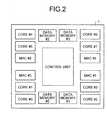
- FIG. 2 is a diagram of a schematic configuration of the CPU according to the second embodiment.
- a CPU 1 is a semiconductor integrated circuit that includes eight cores #0 to #7, four data memories #0 to #3, four MACs #0 to #3, and a control unit.
- the cores #0 to #7, the data memories #0 to #3, and the MACs #0 to #3 are arranged near the periphery of a board, and the control unit is located at the center of the board.
- the cores #0 to #7 are arithmetic processing units that receive data that is temporarily stored in the data memories #0 to #3 and performs various types of arithmetic processing on the data.
- the data on which the arithmetic processing is performed by the cores #0 to #7 is temporarily stored in storage units (not illustrated) (hereinafter, "primary cache") that are respectively provided in the cores #0 to #7 or stored in the data memories #0 to #3.
- the cores #0 to #7 issue, to the control unit, instructions for writing the data that is stored in the primary caches or the data that is stored in the data memories #0 to #3 on a main storage unit (not illustrated).
- the data memories #0 to #3 temporarily store data that the cores #0 to #7 frequently use and the data on which the arithmetic processing is performed by the cores #0 to #7. Specifically, when the control unit performs a write-back process, the data memories #0 to #3 receive the data that is stored in the primary caches of the cores #0 to #7 and stores the received data. When the control unit performs a data-write process, the data memories #0 to #3 output the data stored therein to the MACs #0 to #3.
- the MACs #0 to #3 are main storage control devices that connect to the main storage unit (not illustrated) and that control accesses to the main storage unit. Specifically, the MACs #0 to #3 receive data from the data memories #0 to #3 and write the data to the main storage unit.
- the control unit performs the data-write process or the write-back process by pipeline processing.
- the data-write process is a process for writing back the latest data that is stored in the primary caches of the cores #0 to #7 to the main storage unit, or for writing back the data that is stored in the data memories #0 to #3 to the main storage unit.
- the write-back process is a process for writing back the data that is stored in the primary caches of the cores #0 to #7 to the data memories #0 to #3.
- FIG. 3 is a diagram of a main configuration of the CPU 1 according to the second embodiment.
- FIG. 3 particularly illustrates the parts corresponding to the cores #0 to #3, the data memories #0 and #1, and the MACs #0 and #1 of the CPU 1 illustrated in FIG. 2 .
- the CPU 1 illustrated in FIG. 3 includes a control unit 101, a first queue 102, a second queue 103, a third queue 104, a selector 105, a data memory 106, selectors 107 and 108, and a connecting unit L0.
- the CPU 1 further includes cores 200a and 200b and an MAC 300. Because the CPU 1 illustrated in FIG. 3 has a symmetrical configuration, reference numerals are given to only the left half of the diagram.
- the cores 200a and 200b perform various types of arithmetic processing using the data that is stored in the main storage unit (not illustrated) connected to the MAC 300, or the data that is stored in the data memory 106.
- the cores 200a and 200b issue a request for data to be used for arithmetic processing to the control unit 101.
- the cores 200a and 200b read the data from the data memory 106 by a data-read process.
- the cores 200a and 200b transfer the data from the main storage unit to the data memory 106 via the MAC 300 and the third queue 104, and then receive the data from the data memory 106.
- the cores 200a and 200b After the cores 200a and 200b complete the arithmetic processing, the cores 200a and 200b store the data that is processed by the arithmetic processing in the primary caches (not illustrated) of the cores 200a and 200b.
- the cores 200a and 200b then issue, to the control unit 101, an instruction for performing the data-write process for writing data to the main storage unit.
- the cores 200a and 200b according to the second embodiment issue an instruction for performing the data-write process for writing the data stored in the primary caches directly to the main storage unit, in addition to the instruction for performing the existing data-write process for writing the data stored in the primary caches to the main storage unit via the data memory.
- the control unit 101 performs the write-back process and the data-write process according to instructions from the cores 200a and 200b. In addition to these processes, the control unit 101 also performs the data-read process for reading data that is requested by the cores 200a and 200b from the data memory 106 and a move-in process for transferring data requested by the cores 200a and 200b from the main storage unit to the data memory when a cache miss occurs.
- control unit 101 When inputting instructions, such as the data-write request or the write-back request from the cores 200a and 200b, to the pipeline, the control unit 101 inputs the instructions to the pipeline at appropriate intervals such that a plurality of instructions do not cause interference that simultaneously uses resources, such as the data memory 106. This will be described below.
- the first queue 102 is a queue that temporarily stores the data that is to be written back from the cores 200a and 200b to the data memory 106 when the write-back process is performed. Specifically, the first queue 102 temporarily stores the data that is processed by the arithmetic processing in the cores 200a and 200b, and outputs the data under the control of the control unit 101.
- the first queue 102 is provided near the input part of the data memory 106 in consideration of wiring.
- the first queue 102 may be referred to as, for example, a write back data queue (WBDQ).
- WBDQ write back data queue
- the second queue 103 is a queue that temporarily stores the data that is to be written back from the data memory 106 to the main storage unit (not illustrated) via the MAC 300 when the data-write process is performed. Specifically, the second queue 103 temporarily stores the data that is received via the selector 108, and outputs the data to the MAC 300 under the control of the control unit 101.
- the second queue 103 is provided near the MAC 300 in consideration of wiring.
- the second queue 103 may be referred to as, for example, a move out data queue (MODQ).
- the third queue 104 is a queue that temporarily stores the data that is to be transferred from the MAC 300 to the data memory 106 when the move-in process is performed on the occurrence of a cache miss. Specifically, the third queue 104 temporarily stores the data from the MAC 300, which data is requested by the cores 200a and 200b, and outputs the data to the data memory 106 via the selector 105.
- the third queue 104 is provided near the input part of the data memory 106 in consideration of wiring as the first queue 102 is.
- the third queue 104 may be referred to as, for example, a move in data queue (MIDQ).
- the selector 105 selects any one of the data that is stored in the first queue 102 and the data that is stored in the third queue 104, and outputs the data to the data memory 106. Specifically, when the control unit 101 performs the write-back process, the selector 105 selects the data stored in the first queue 102. When the control unit 101 performs the move-in process, the selector 105 selects the data stored in the third queue 104.
- the data memory 106 temporarily stores the data that is used by the cores 200a and 200b and the data that is processed by the arithmetic processing in the cores 200a and 200b. Specifically, when the control unit 101 performs the write-back process, the data memory 106 receives the data that is output from the primary caches of the cores to the first queue 102, and stores the received data. When the control unit 101 performs the data-write process, the data memory 106 outputs the data, which is received from the first queue 102, to the selector 107. For example, a random access memory (RAM) may be used for the data memory 106.
- RAM random access memory
- the connecting unit L0 is wiring that connects the data path from the cores 200a and 200b to the data memory 106 (hereinafter, "input path") and the data path from the data memory 106 to the MAC 300 (hereinafter, “output path”). Specifically, the connecting unit L0 connects the input path between the first queue 102 and the data memory 106 and the selector 107. In other words, the connecting unit L0 connects to the input path near the data memory 106.
- the connecting unit L0 transfers the data that is output from the first queue 102 to the selector 107, avoiding the data memory 106.
- the CPU 1 according to the second embodiment can output the data that is output from the first queue 102 directly to the MAC 300 without going via the data memory 106.
- the selector 107 is a selecting unit that is provided on the output path of the data memory 106.
- the selector 107 selects any one of the data that is output from the first queue 102 via the connecting unit L0 and the data that is output from the data memory 106, and outputs the data to the selector 108.
- the selector 107 transfers the data, which is output from the first queue 102, to the selector 108 via the connecting unit L0 under the control of the control unit 101.
- the selector 107 transfers the data, which is output from the data memory 106, to the selector 108 under the control of the control unit 101.
- the selector 108 selects any one of the data that is output from the selector 107 and data that is output from another selector corresponding to the selector 107, and outputs the data to the MAC 300. Specifically, when the data that is stored in the cores 200a and 200b or the data memory 106 is transferred to the MAC 300, the selector 108 selects the data that is output from the selector 107. In contrast, when data that is stored in a core other than the cores 200a and 200b or in a data memory other than the data memory 106 is transferred to the MAC 300, the selector 108 selects the data that is output from another selector corresponding to the selector 107.
- the MAC 300 is connected to the main storage unit (not illustrated) that stores all data that the cores 200a and 200b may use, and controls accesses to the main control unit. Specifically, the MAC 300 writes the data, which is stored in the second queue 103, to the main storage unit. Note that, as another process, when a cache miss occurs, the MAC 300 receives the cache miss data and then transfers the data to the third queue 104.
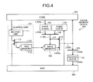
- FIG. 4 is a diagram illustrating the connection relationship in the cache memory device according to the second embodiment.
- the same parts in FIG. 4 as those in FIG. 2 are denoted by the same reference numerals and explanation thereof will be omitted.
- a cache memory device 100 includes the control unit 101, the first queue 102, the second queue 103, the third queue 104, the selectors 105, 107, and 108, and the data memory 106.
- the control unit 101 performs the write-back process and the data-write process according to a data-write request from a core 200.
- the control unit 101 includes an MO port unit 111, a priority unit 112, a pipeline 113, and a tag memory 114.
- the MO port unit 111 receives instructions, such as the data-write request, from the core 200.
- the data-write request include, in addition to the existing data-write request for writing data via the data memory 106, a data-write request for writing data that is stored in the primary cache of the core 200 directly to the main storage unit.
- the core 200 outputs a movement bypass and tag invalidate (MB-IV) to the MO port unit 111 as the data-write request.
- MB-IV movement bypass and tag invalidate
- the priority unit 112 adjusts instructions that are received by the MO port unit 111 in consideration of priority in data paths and various resources, and inputs the instructions to the pipeline 113. Specifically, when the MO port unit 111 receives the MB-IV, the priority unit 112 generates a bypass moveout (BPMO) as internal operation codes and inputs the BPMO to the pipeline 113.
- BPMO bypass moveout
- a buffer (not illustrated) that stores a move-in request, which is issued on the occurrence of a cache miss, is provided between the MAC 300 and the priority unit 112. The priority unit 112 also adjusts the move-in request that is stored in the buffer.
- the buffer may be referred to as, for example, a move-in (MI) buffer.
- the tag memory 114 stores the physical addresses and type codes of the data that is stored in the data memory 106 and stores logical addresses that are used for local buffer storage tag (LBSTAG) search.
- the pipeline 113 searches the tag memory 114 according to instructions that are input from the priority unit 112 and specifies the physical address of the data.
- the pipeline 113 updates or transfers the data that is stored in the specified physical address according to the input instructions.
- the control unit 101 Upon receiving the existing data-write request from the core 200, first, as the write-back process, the control unit 101 writes the data that is stored in the primary cache of the core 200 to the data memory 106 using input paths L100a to L100c.
- the data stored in the primary cache of the core 200 is first transferred to the first queue 102 from the core 200 via the input path L100a. Subsequently, the data stored in the first queue 102 is transferred to the selector 105 via the input path L100b.
- the selector 105 selects the data from the input path L100b and transfers the data to the data memory 106 via the input path L100c.
- the data memory 106 receives the data that is transferred via the input path L100c, i.e., the data that is stored in the primary cache of the core 200, and stores the data. Accordingly, the write-back process completes.
- the control unit 101 transfers the data that is stored in the data memory 106 to the MAC 300 using the output paths L200a to L200d.
- the data that is stored in the data memory 106 is first transferred to the selector 107 via the output path L200a.
- the selector 107 selects the data from the output path L200a and transfers the data to the second queue 103 via the output path L200b, the selector 108, and the output path L200c.
- the data that is stored in the second queue 103 is then transferred to the MAC 300 via the output path L200d and written back by the MAC 300 to the main storage unit. Accordingly, the data stored in the main storage unit becomes the latest, which maintains the data coherency (cache coherency).
- the selector 107 is provided near the data memory.
- the connecting unit L0 that connects the input path L100c and the selector 107 is a very short line that is provided to only around the data memory 106.
- the control unit 101 receives at the MO port unit 111 the MB-IV as the data-write request from the core 200.
- the control unit 101 transfers the data that is stored in the primary cache of the core 200 directly to the MAC 300, using the connecting unit L0. Specifically, this data transfer is performed when the data is exclusively stored, the latest data is stored in the primary cache of the core 200, and only old data is stored in the data memory 106.
- the data that is stored in the primary cache of the core 200 is first transferred from the core 200 to the first queue 102 via the input path L100a. Subsequently, under the control of the control unit 101, the data that is stored in the first queue 102 is transferred to the selector 105 via the input path L100b. Subsequently, under the control of the control unit 101, the selector 105 selects the data from the input path L100b and transfers the selected data to the input path L100c.
- the selector 107 Under the control of the control unit 101, the selector 107 then receives the data that is output from the selector 105 via an input path 100c and the connecting unit L0, and transfers the data to the second queue 103 via the output path L200b, the selector 108, and the output path L200c.
- the following steps are similar to those performed when the latest data is stored in the data memory 106, i.e., the MAC 300 writes back the data, which is stored in the second queue 103, to the main storage unit and the data-write process is completed accordingly.
- the data paths utilize the input paths L100a to L100c that are used for performing the write-back process and the output paths L200b to L200d that are used for performing the process for writing data from the data memory 106 to the main storage unit. This reduces wiring costs and allows easily mounting the data paths on the CPU 1 that includes the multiple cores and multi-bank memories.
- the input paths L100a to L100c are used commonly to write back data from the core 200 to the data memory 106 and to write data from the core 200 to the main storage unit via the connecting unit L0.
- the output paths L200b to L200d are used commonly to write data from the core 200 to the main storage unit via the connecting unit L0 and to write data stored in the data memory 106 to the main storage unit. Therefore, when another process is performed while each of the above processes is performed, data interference may occur.
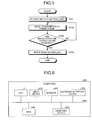
- FIG. 5 is a flowchart of a process procedure of the control unit 101 according to the second embodiment.
- FIG. 5 illustrates only a process procedure, among process procedures performed by the control unit 101, of the data-write process for directly transferring data that is stored in the primary cache of the core 200 directly to the MAC 300.
- control unit 101 first receives, at the MO port unit 111, the MB-IV that requests transferring the data that is stored in the primary cache memory of the core 200 directly to the MAC 300 (step S101). The control unit 101 then makes adjustments, at the priority unit 112, such that no data interference between instructions occurs (step S102).
- the control unit 101 determines, at the priority unit 112, whether the input paths L100a to L100c and the output paths L200ato L200d are available (step S103). In other words, the priority unit 112 determines whether the input paths L100a to L100c are being used because of the write-back process, and whether the output paths L200a to L200d are being used because of the process for writing data from the data memory 106. When the input paths L100a to L100c and the output paths L200a to L200d are not being used, the control unit 101 determines that the input paths L100a to L100c and the output paths L200a to L200d are available.
- the priority unit 112 makes adjustments such that the MB-IV waits in the MO port unit 111 until these paths become available.
- the data is not transferred from the core 200 directly to the MAC 300.
- the priority unit 112 When it is determined that the input paths L100a to L100c and the output paths L200a to L200d are available (YES at step S103), the priority unit 112 generates an internal operation code BPMO and inputs the BMPO to the pipeline (step S104).
- the conditions for the control unit 101 to determine that the input paths L100a to L100c and the output paths L200a too L200d are available include the case where the time at which the waiting instruction starts to be executed.
- the latest data that is stored in the primary cache of the core 200 is output to the first queue 102.
- the latest data that is stored in the first queue 102 is then transferred via the selector 105 to the input paths L100c.
- the selector 107 Under the control of the control unit 101, the selector 107 receives the data that is output from the selector 105 via the input path 100c and the connecting unit L0, and transfers the data to the output path L200b.
- the latest data is transferred to the second queue 103 via the output path L200b, the selector 108, and the output path L200c, and is written back by the MAC 300 to the main storage unit.
- control unit 101 when the control unit 101 receives the data-write instruction for writing the data from the core 200 to the main storage unit and the input paths L100a to L100c or the output paths L200a to L200d are being used because of the process according to another instruction, the control unit 101 waits starting to perform the process according to the data-write instruction until the use of the paths completes. In other words, the control unit 101 inputs the BPMO to the pipeline 113 under the condition that the input paths L100a to L100c and the output paths L200a to L200d are not being used. Accordingly, occurrence of data interference between the write-back process and the process for writing data from the data memory 106 can be prevented.
- control unit 101 While performing the data-write process for writing the data from the core 200 to the main storage unit, the control unit 101 waits for starting to perform a process, such as the write-back process or the move-in process, that uses the input paths. Furthermore, while performing the process for writing the data from the core 200 to the main storage unit, the control unit 101 waits for starting to perform a process, such as writing data from the data memory 106 to the main storage unit, using the output paths.
- a process such as the write-back process or the move-in process
- the control unit 101 When the process for writing the data from the core 200 to the main storage unit is completed and the time at which the waiting instruction starts to be executed, the control unit 101. inputs the instruction to the pipeline to start performing the process according to the instruction. Because, in this manner, the control unit 101 waits for starting to perform another process using the input paths or the output paths while performing the data-write process for writing the data from the core 200 to the main storage unit, data interference can be prevented more assuredly.
- the control unit 101 controls the selector 107 such that it selects the data from the output path L200a. Accordingly, the latest data is transferred from the data memory 106 via the output path L200a to the selector 107. The latest data is then transferred to the second queue 103 via the output path L200b, the selector 108, and the output path L200c, and is written back by the MAC 300 to the main storage unit.
- the connecting unit L0 and the selector 107 with a small increase in physical costs because of adding the connecting unit L0 and the selector 107, higher physical costs for assuring the data paths that directly connect each core 200 and each MAC 300 as in the conventional technologies can be reduced. Furthermore, in the second embodiment, only the connecting unit L0 provided in a short line and the selector 107 are added and they can be easily provided in an area in a CPU where wiring is concentrated. Accordingly, an increase in the circuit size can be reduced, which is highly efficient regarding the number of transistors to be mounted and wiring. Thus, the data paths for transferring data from the core 200 directly to the MAC 300 can be mounted on the CPU that includes multiple cores 200 and the MAC 300.
- the steps in which the control unit 101 controls the selector 107 are only added to the existing steps using the steps of the write-back process and the process for writing data from the data memory 106 to the main storage unit. Therefore, the control complexity can be reduced. This reduces effects on the performance as a CPU.
- the CPU 1 according to the second embodiment is mounted on an arithmetic processing apparatus, such as a personal computer (PC).
- FIG. 6 is a block diagram of an example of a computer on which the CPU 1 according to the second embodiment is mounted.
- a computer 600 that is an arithmetic processing apparatus includes the CPU 1, an input device 610, a monitor 620, a network interface device 630, a RAM 640, and a hard disk device 650.
- the computer 600 connects these devices with a bus 660.
- the input device 610 is for example a keyboard and a mouse, and receives data inputs from users.
- the monitor 620 is a display unit that displays various types of information.
- the network interface device 630 communicates data with other computers via networks, such as the Internet.
- the RAM 640 corresponds to the main storage unit and temporarily stores various types of information.
- the hard disk device 650 is a non-volatile storage device.
- the invention also provides a computer program or a computer program product for carrying out any of the methods described herein, and a computer readable medium having stored thereon a program for carrying out any of the methods described herein.
- a computer program embodying the invention may be stored on a computer-readable medium, or it could, for example, be in the form of a signal such as a downloadable data signal provided from an Internet website, or it could be in any other form.
Landscapes
- Engineering & Computer Science (AREA)
- Theoretical Computer Science (AREA)
- Physics & Mathematics (AREA)
- General Engineering & Computer Science (AREA)
- General Physics & Mathematics (AREA)
- Memory System Of A Hierarchy Structure (AREA)
Abstract
Description
- The embodiments discussed herein are directed to a processor and a processing method.
- Recent arithmetic processing apparatuses that include processor cores, such as a CPU, are generally provided with cache memories to increase processing speeds. A cache memory is provided between a main storage unit, such as a main memory, and a processor core and temporarily stores data that the processor core frequently uses. When executing arithmetic processing, the processor core reads the data from the cache memory, which is closer to the processor core than to the main memory, so that the time required for memory access can be shortened.
- In conventional arithmetic processing apparatuses, data that is processed through arithmetic processing by a processor core is temporarily stored in a cache memory and the data is written to a main storage unit at predetermined intervals of time. However, when data is written to the main storage unit via the cache memory, the time required for writing the data becomes accordingly longer (see, for example, Japanese Laid-open Patent Publication No.
63-20640 FIG. 7 illustrates one example of an arithmetic processing apparatus that is provided with such a data path. - As illustrated in
FIG. 7 , an arithmetic processing apparatus 500 includes a processor core (hereinafter, "core") 501, a first queue, 502 asecond queue 503, and athird queue 504. The arithmetic processing apparatus 500 further includes aselector 505, adata memory 506, acontrol unit 507, and a memory access controller (MAC) 508. - The
core 501 is an arithmetic processing unit that executes various types of arithmetic processing using data that is stored in thedata memory 506. Thefirst queue 502 is a queue that temporarily stores data that is written back to thedata memory 506 from thecore 501. Thesecond queue 503 is a queue that temporarily stores data that is written back to a main storage unit (not illustrated) from thedata memory 506 via the MAC 508 when a cache replacement is performed. Thethird queue 504 is a queue that temporarily stores data that is transferred to thedata memory 506 from the MAC 508 when a move in is performed on the occurrence of a cache miss. - The
selector 505 selects any one of the data that is stored in thefirst queue 502 and the data that is stored in thethird queue 504 and outputs the selected data to thedata memory 506. Thedata memory 506 temporarily stores data that is frequently used by thecore 501 and data that is processed by arithmetic processing in thecore 501. Thecontrol unit 507 writes or reads data by pipeline processing according to instructions from thecore 501. Specifically, thecontrol unit 507 includes a move-out (MO)port unit 511, apriority unit 512, apipeline 513, and atag memory 514. - Order responses from the
core 501, such as data writing and data reading, are set by theMO port unit 511. Thepriority unit 512 makes adjustments (data interference control) and inputs data to thepipeline 513. Thetag memory 514 stores physical addresses of the data that is stored in thedata memory 506 and stores logical addresses that are used for searching tags. When a data writing request is input from thepriority unit 512, thepipeline 513 searches thetag memory 514 according to the logical address contained in the request and specifies the physical address of the data that is requested by thecore 501. The MAC 508 is connected to the main storage unit (not illustrated) and writes data that is received from thesecond queue 503 to the main storage unit. If a cache miss occurs, for example, the MAC 508 receives the cache miss data from the main storage unit and transfers the cache miss data to thethird queue 504. - In this case, if the latest data is stored in the
data memory 506, a data path L20 from thedata memory 506 to the MAC 508 is used to write the data to the main storage unit. For writing back data to thedata memory 506 from thecore 501, a data path L10 is used that extends from thecore 501 to thedata memory 506 via thefirst queue 502 and theselector 505. - If the latest data is stored in the
core 501 and thedata memory 506 stores only old data, a data path L30 for transferring data from thecore 501 directly to the MAC 508 is used to write data to the MAC 508. Because a data path L30 that directly connects thecore 501 and the MAC 508 is provided, the latest data that is stored in thecore 501 can be quickly written to the main storage unit without going via thedata memory 506. - However, newly providing a data path that directly connects a core and an MAC increases wiring costs. This is apparent particularly in a CPU including multiple cores and multi-bank storage units. These problems are specifically explained below.
- Increases in power consumption in recent single-core CPUs, each of which includes one core, is not ignorable and the performance improvement is approaching its limit. Approaches to further improve the CPU performance are made in some cases using a multi-core CPU that includes multiple cores on a board. Furthermore, in addition to providing multiple cores, approaches to improve the throughput between each core and the cache memory or the main storage unit are made in some cases by dividing the cache memory and the main storage unit into banks.
FIG. 8 is a diagram of a schematic configuration of a conventional CPU. - As illustrated in
FIG. 8 , in aCPU 700 that includes multiple cores and multi-bank storage units,cores # 0 to #7,data memories # 0 to #3, andMACs # 0 to #3 are arranged near the periphery of the board. At the center of the board, a control unit that controls the entire data transfer is located. Because the multi-bank main storage units respectively store different types of data, each of thecores # 0 to #7 may write data to all of theMACs # 0 to #3. Therefore, all the cores may be connected to all the MACs to provide data paths that directly connect the cores and the MACs, which increases wiring costs. - More specifically, in the
CPU 700, a data path L30 that connects the cores and the MACs is provided between all of thecores # 0 to #3 and all of theMACs # 0 to #3. For example, as illustrated inFIG. 8 , thecore # 1 is provided with data paths L30a to L30d that connect to therespective MACs # 0 to #3. Note that thecore # 1 is further provided with data paths L20a to L20d that connect to thedata memories # 0 to #3, and thedata memories # 0 to #3 are provided respectively with data path L10a to L10d that connect to thecorresponding MACs # 0 to #3. - Among the data paths, particularly, the data path L30b and the data path L30d may be provided across the control unit that is located at the center of the board, which may increase wiring costs. Therefore, it has been difficult to mount a data path L30 that directly connects the cores and the MACs in the
CPU 700, including the multiple cores and the multi-bank storage units. The areas A1 and A2, illustrated inFIG. 8 , between the cores and the MACs and the data memories and the control unit are areas where wiring is particularly concentrated. Because providing the data path L30 in such areas results in an increase in the circuit size, mounting the data path is difficult. - Accordingly, it is desirable to provide a cache memory device that reduces wiring costs and shortens the time required for writing data from an arithmetic processing unit to a main memory, a semiconductor integrated circuit, and an arithmetic processing apparatus.
- According to an embodiment of an aspect of the invention, a processor includes: a data memory that stores data that is written by an arithmetic processing unit that performs arithmetic processing; a connecting unit that connects an input path from the arithmetic processing unit to the data memory and an output path from the data memory to a main storage unit; a selecting unit that is provided on the output path, selects any one of data that is output from the data memory or data that is transferred from the arithmetic processing unit via the connecting unit, and transfers the selected data to the output path; and a control unit that controls the selecting unit such that the data that is output from the data memory is transferred to the output path when the data is written from the data memory to the main storage unit, and controls the selecting unit such that the data is transferred to the output path via the connecting unit when the data is written from the arithmetic processing unit to the main storage unit.
- According to an embodiment of another aspect of the invention, a processing method for a processor including an input path from an arithmetic processing unit to a data memory that stores data written by the arithmetic processing unit that performs arithmetic processing, and an output path from the data memory to a main storage unit, the processing method includes: selecting data that is output from the data memory when the data is written from the data memory to the main storage unit, and selecting the data that is transferred from the arithmetic processing unit via the input path when the data is written from the arithmetic processing unit to the main storage unit; and transferring the selected data to the main storage unit.
-
-
FIG. 1 is a diagram illustrating a connection relationship in a cache memory device according to a first embodiment of the present invention; -
FIG. 2 is a diagram of a schematic configuration of a CPU according to a second embodiment of the present invention; -
FIG. 3 is a diagram of a main configuration of the CPU according to the second embodiment of the present invention; -
FIG. 4 is a diagram illustrating a connection relationship in a cache memory device according to the second embodiment of the present invention; -
FIG. 5 is a flowchart of a process procedure of a control unit according to the second embodiment; -
FIG. 6 is a block diagram of an example of a computer that mounts the CPU according to the second embodiment; -
FIG. 7 is a diagram of an example of a conventional arithmetic processing apparatus; and -
FIG. 8 is a diagram of a schematic configuration of a conventional CPU. - Embodiments of the present invention will be explained with reference to accompanying drawings. Note that the embodiments do not limit the present invention.
-
FIG. 1 is a diagram illustrating a connection relationship in a cache memory device according to a first embodiment of the present invention. Acache memory device 10 according to the first embodiment is a storage device that speeds up data communications between anarithmetic processing unit 20 and a main storage unit. As illustrated inFIG. 1 , thecache memory device 10 is provided between thearithmetic processing unit 20 and amain storage unit 30. Themain storage unit 30 is a storage unit that stores data. Thearithmetic processing unit 20 performs various types of arithmetic processing using the data that is stored in themain storage unit 30. - The
cache memory device 10 includes a data memory 11, a connecting unit 12, a control unit 13, and a selectingunit 14. The data memory 11 temporarily stores data on which the arithmetic processing is performed by thearithmetic processing unit 20. Specifically, the data memory 11 temporarily stores data that is transferred from thearithmetic processing unit 20 via an input path L50 as illustrated inFIG. 1 . - The connecting unit 12 is wiring that connects the input path L50 from the
arithmetic processing unit 20 to the data memory 11 and an output path L60 from the data memory 11 to themain storage unit 30. The selectingunit 14 is provided on the output path L60. Under the control of the control unit 13, the selectingunit 14 selects any one of the data that is output from the data memory 11 and the data that is transferred from thearithmetic processing unit 20 via the connecting unit 12, and transfers the selected data to themain storage unit 30. - In other words, to write the data stored in the data memory 11 to the
main storage unit 30, the control unit 13 controls the selectingunit 14 and causes the selectingunit 14 to select the data that is output from the data memory 11. The selectingunit 14 then transfers the selected data to themain storage unit 30 via the output path L60. - In contrast, to write the data from the
arithmetic processing unit 20 directly to themain storage unit 30, the control unit 13 controls the selectingunit 14 and causes the data to be transferred to the selectingunit 14 via the connecting unit 12. The selectingunit 14 then transfers the data to themain storage unit 30 via the output path L60. In this manner, the data on which the arithmetic processing is performed by thearithmetic processing unit 20 is written to themain storage unit 30 via thearithmetic processing unit 20, the input path L50, the connecting unit 12, the selectingunit 14, and the output path L60. - As described above, in the first embodiment, because the path for writing data from the
arithmetic processing unit 20 directly to themain storage unit 30, avoiding the data memory 11, is provided, the time required for writing data from thearithmetic processing unit 20 to themain storage unit 30 can be shortened. Furthermore, because the data path can be provided utilizing the input path L50 from thearithmetic processing unit 20 to the data memory 11 and the output path L60 from the data memory 11 to themain storage unit 30, wiring costs can be reduced. - In the first embodiment, wiring costs are reduced and the time necessary for writing data from the
arithmetic processing unit 20 to themain storage unit 30 can be shortened. - A cache memory device, a semiconductor integrated circuit, and an arithmetic processing apparatus according to a second embodiment of the present invention will be explained. As an example of the semiconductor integrated circuit, a CPU in which a plurality of cores, a plurality of memories, and a plurality of MACs are arranged is used for explanation. Note that the technology disclosed in this application can be applied to a CPU in which a core, a data memory, and a MAC are arranged on a single board.
-
FIG. 2 is a diagram of a schematic configuration of the CPU according to the second embodiment. As illustrated inFIG. 2 , aCPU 1 is a semiconductor integrated circuit that includes eightcores # 0 to #7, fourdata memories # 0 to #3, fourMACs # 0 to #3, and a control unit. In theCPU 1, thecores # 0 to #7, thedata memories # 0 to #3, and theMACs # 0 to #3 are arranged near the periphery of a board, and the control unit is located at the center of the board. - The
cores # 0 to #7 are arithmetic processing units that receive data that is temporarily stored in thedata memories # 0 to #3 and performs various types of arithmetic processing on the data. For example, the data on which the arithmetic processing is performed by thecores # 0 to #7 is temporarily stored in storage units (not illustrated) (hereinafter, "primary cache") that are respectively provided in thecores # 0 to #7 or stored in thedata memories # 0 to #3. Thecores # 0 to #7 issue, to the control unit, instructions for writing the data that is stored in the primary caches or the data that is stored in thedata memories # 0 to #3 on a main storage unit (not illustrated). - The
data memories # 0 to #3 temporarily store data that thecores # 0 to #7 frequently use and the data on which the arithmetic processing is performed by thecores # 0 to #7. Specifically, when the control unit performs a write-back process, thedata memories # 0 to #3 receive the data that is stored in the primary caches of thecores # 0 to #7 and stores the received data. When the control unit performs a data-write process, thedata memories # 0 to #3 output the data stored therein to theMACs # 0 to #3. - The
MACs # 0 to #3 are main storage control devices that connect to the main storage unit (not illustrated) and that control accesses to the main storage unit. Specifically, theMACs # 0 to #3 receive data from thedata memories # 0 to #3 and write the data to the main storage unit. - The control unit performs the data-write process or the write-back process by pipeline processing. The data-write process is a process for writing back the latest data that is stored in the primary caches of the
cores # 0 to #7 to the main storage unit, or for writing back the data that is stored in thedata memories # 0 to #3 to the main storage unit. The write-back process is a process for writing back the data that is stored in the primary caches of thecores # 0 to #7 to thedata memories # 0 to #3. -
FIG. 3 is a diagram of a main configuration of theCPU 1 according to the second embodiment.FIG. 3 particularly illustrates the parts corresponding to thecores # 0 to #3, thedata memories # 0 and #1, and theMACs # 0 and #1 of theCPU 1 illustrated inFIG. 2 . - The
CPU 1 illustrated inFIG. 3 includes acontrol unit 101, afirst queue 102, asecond queue 103, athird queue 104, aselector 105, adata memory 106,selectors CPU 1 further includescores MAC 300. Because theCPU 1 illustrated inFIG. 3 has a symmetrical configuration, reference numerals are given to only the left half of the diagram. - The
cores MAC 300, or the data that is stored in thedata memory 106. - For example, the
cores control unit 101. When the data is stored in the data memory 106 (cache hit), thecores data memory 106 by a data-read process. In contrast, when the data to be used for the arithmetic processing is not stored in the data memory 106 (cache miss), thecores data memory 106 via theMAC 300 and thethird queue 104, and then receive the data from thedata memory 106. - After the
cores cores cores cores control unit 101, an instruction for performing the data-write process for writing data to the main storage unit. Specifically, thecores - The
control unit 101 performs the write-back process and the data-write process according to instructions from thecores control unit 101 also performs the data-read process for reading data that is requested by thecores data memory 106 and a move-in process for transferring data requested by thecores - When inputting instructions, such as the data-write request or the write-back request from the
cores control unit 101 inputs the instructions to the pipeline at appropriate intervals such that a plurality of instructions do not cause interference that simultaneously uses resources, such as thedata memory 106. This will be described below. - The
first queue 102 is a queue that temporarily stores the data that is to be written back from thecores data memory 106 when the write-back process is performed. Specifically, thefirst queue 102 temporarily stores the data that is processed by the arithmetic processing in thecores control unit 101. Thefirst queue 102 is provided near the input part of thedata memory 106 in consideration of wiring. Thefirst queue 102 may be referred to as, for example, a write back data queue (WBDQ). - The
second queue 103 is a queue that temporarily stores the data that is to be written back from thedata memory 106 to the main storage unit (not illustrated) via theMAC 300 when the data-write process is performed. Specifically, thesecond queue 103 temporarily stores the data that is received via theselector 108, and outputs the data to theMAC 300 under the control of thecontrol unit 101. Thesecond queue 103 is provided near theMAC 300 in consideration of wiring. Thesecond queue 103 may be referred to as, for example, a move out data queue (MODQ). - The
third queue 104 is a queue that temporarily stores the data that is to be transferred from theMAC 300 to thedata memory 106 when the move-in process is performed on the occurrence of a cache miss. Specifically, thethird queue 104 temporarily stores the data from theMAC 300, which data is requested by thecores data memory 106 via theselector 105. Thethird queue 104 is provided near the input part of thedata memory 106 in consideration of wiring as thefirst queue 102 is. Thethird queue 104 may be referred to as, for example, a move in data queue (MIDQ). - The
selector 105 selects any one of the data that is stored in thefirst queue 102 and the data that is stored in thethird queue 104, and outputs the data to thedata memory 106. Specifically, when thecontrol unit 101 performs the write-back process, theselector 105 selects the data stored in thefirst queue 102. When thecontrol unit 101 performs the move-in process, theselector 105 selects the data stored in thethird queue 104. - The
data memory 106 temporarily stores the data that is used by thecores cores control unit 101 performs the write-back process, thedata memory 106 receives the data that is output from the primary caches of the cores to thefirst queue 102, and stores the received data. When thecontrol unit 101 performs the data-write process, thedata memory 106 outputs the data, which is received from thefirst queue 102, to theselector 107. For example, a random access memory (RAM) may be used for thedata memory 106. - The connecting unit L0 is wiring that connects the data path from the
cores data memory 106 to the MAC 300 (hereinafter, "output path"). Specifically, the connecting unit L0 connects the input path between thefirst queue 102 and thedata memory 106 and theselector 107. In other words, the connecting unit L0 connects to the input path near thedata memory 106. - The connecting unit L0 transfers the data that is output from the
first queue 102 to theselector 107, avoiding thedata memory 106. In other words, because the connecting unit L0 is provided, theCPU 1 according to the second embodiment can output the data that is output from thefirst queue 102 directly to theMAC 300 without going via thedata memory 106. - The
selector 107 is a selecting unit that is provided on the output path of thedata memory 106. Theselector 107 selects any one of the data that is output from thefirst queue 102 via the connecting unit L0 and the data that is output from thedata memory 106, and outputs the data to theselector 108. Specifically, when data is transferred from thecores MAC 300, theselector 107 transfers the data, which is output from thefirst queue 102, to theselector 108 via the connecting unit L0 under the control of thecontrol unit 101. When data that is stored in thedata memory 106 is transferred directly to theMAC 300, theselector 107 transfers the data, which is output from thedata memory 106, to theselector 108 under the control of thecontrol unit 101. - The
selector 108 selects any one of the data that is output from theselector 107 and data that is output from another selector corresponding to theselector 107, and outputs the data to theMAC 300. Specifically, when the data that is stored in thecores data memory 106 is transferred to theMAC 300, theselector 108 selects the data that is output from theselector 107. In contrast, when data that is stored in a core other than thecores data memory 106 is transferred to theMAC 300, theselector 108 selects the data that is output from another selector corresponding to theselector 107. - The
MAC 300 is connected to the main storage unit (not illustrated) that stores all data that thecores MAC 300 writes the data, which is stored in thesecond queue 103, to the main storage unit. Note that, as another process, when a cache miss occurs, theMAC 300 receives the cache miss data and then transfers the data to thethird queue 104. - Subsequently, the connection relationship between the cores, the MACs, and the cache memory device according to the second embodiment will be explained in detail with reference to
FIG. 4. FIG. 4 is a diagram illustrating the connection relationship in the cache memory device according to the second embodiment. The same parts inFIG. 4 as those inFIG. 2 are denoted by the same reference numerals and explanation thereof will be omitted. - As illustrated in
FIG. 4 , acache memory device 100 includes thecontrol unit 101, thefirst queue 102, thesecond queue 103, thethird queue 104, theselectors data memory 106. - The
control unit 101 performs the write-back process and the data-write process according to a data-write request from acore 200. Specifically, thecontrol unit 101 includes anMO port unit 111, apriority unit 112, a pipeline 113, and atag memory 114. TheMO port unit 111 receives instructions, such as the data-write request, from thecore 200. In the second embodiment, the data-write request include, in addition to the existing data-write request for writing data via thedata memory 106, a data-write request for writing data that is stored in the primary cache of the core 200 directly to the main storage unit. When the data stored in the primary cache is transferred directly to theMAC 300, thecore 200 outputs a movement bypass and tag invalidate (MB-IV) to theMO port unit 111 as the data-write request. - The
priority unit 112 adjusts instructions that are received by theMO port unit 111 in consideration of priority in data paths and various resources, and inputs the instructions to the pipeline 113. Specifically, when theMO port unit 111 receives the MB-IV, thepriority unit 112 generates a bypass moveout (BPMO) as internal operation codes and inputs the BPMO to the pipeline 113. A buffer (not illustrated) that stores a move-in request, which is issued on the occurrence of a cache miss, is provided between theMAC 300 and thepriority unit 112. Thepriority unit 112 also adjusts the move-in request that is stored in the buffer. The buffer may be referred to as, for example, a move-in (MI) buffer. - The
tag memory 114 stores the physical addresses and type codes of the data that is stored in thedata memory 106 and stores logical addresses that are used for local buffer storage tag (LBSTAG) search. The pipeline 113 searches thetag memory 114 according to instructions that are input from thepriority unit 112 and specifies the physical address of the data. The pipeline 113 updates or transfers the data that is stored in the specified physical address according to the input instructions. - Upon receiving the existing data-write request from the
core 200, first, as the write-back process, thecontrol unit 101 writes the data that is stored in the primary cache of the core 200 to thedata memory 106 using input paths L100a to L100c. - In other words, the data stored in the primary cache of the
core 200 is first transferred to thefirst queue 102 from thecore 200 via the input path L100a. Subsequently, the data stored in thefirst queue 102 is transferred to theselector 105 via the input path L100b. At this stage, under the control of thecontrol unit 101, theselector 105 selects the data from the input path L100b and transfers the data to thedata memory 106 via the input path L100c. Thedata memory 106 receives the data that is transferred via the input path L100c, i.e., the data that is stored in the primary cache of thecore 200, and stores the data.
Accordingly, the write-back process completes. - Subsequently, as the data-write process, the
control unit 101 transfers the data that is stored in thedata memory 106 to theMAC 300 using the output paths L200a to L200d. In other words, the data that is stored in thedata memory 106 is first transferred to theselector 107 via the output path L200a. Subsequently, under the control of thecontrol unit 101, theselector 107 selects the data from the output path L200a and transfers the data to thesecond queue 103 via the output path L200b, theselector 108, and the output path L200c. The data that is stored in thesecond queue 103 is then transferred to theMAC 300 via the output path L200d and written back by theMAC 300 to the main storage unit. Accordingly, the data stored in the main storage unit becomes the latest, which maintains the data coherency (cache coherency). - The
selector 107 is provided near the data memory. In other words, the connecting unit L0 that connects the input path L100c and theselector 107 is a very short line that is provided to only around thedata memory 106. By providing the connection unit L0 in a short length only around thedata memory 106, an increase in wiring costs can be further reduced and effects on the neighboring wiring can also be reduced. - Assume that a data-write request for writing data from the
core 200 directly to the main storage unit is received from thecore 200, i.e., thecontrol unit 101 receives at theMO port unit 111 the MB-IV as the data-write request from thecore 200. In this case, thecontrol unit 101 transfers the data that is stored in the primary cache of the core 200 directly to theMAC 300, using the connecting unit L0. Specifically, this data transfer is performed when the data is exclusively stored, the latest data is stored in the primary cache of thecore 200, and only old data is stored in thedata memory 106. - In other words, the data that is stored in the primary cache of the
core 200 is first transferred from thecore 200 to thefirst queue 102 via the input path L100a. Subsequently, under the control of thecontrol unit 101, the data that is stored in thefirst queue 102 is transferred to theselector 105 via the input path L100b. Subsequently, under the control of thecontrol unit 101, theselector 105 selects the data from the input path L100b and transfers the selected data to the input path L100c. - Under the control of the
control unit 101, theselector 107 then receives the data that is output from theselector 105 via an input path 100c and the connecting unit L0, and transfers the data to thesecond queue 103 via the output path L200b, theselector 108, and the output path L200c. The following steps are similar to those performed when the latest data is stored in thedata memory 106, i.e., theMAC 300 writes back the data, which is stored in thesecond queue 103, to the main storage unit and the data-write process is completed accordingly. - As described above, in the second embodiment, by providing the data paths for writing data that is processed by the arithmetic processing in the
core 200 directly to the main storage unit (not illustrated), avoiding thedata memory 106, the time required for writing the data from thecore 200 to the main storage unit can be shortened. Furthermore, the data paths utilize the input paths L100a to L100c that are used for performing the write-back process and the output paths L200b to L200d that are used for performing the process for writing data from thedata memory 106 to the main storage unit. This reduces wiring costs and allows easily mounting the data paths on theCPU 1 that includes the multiple cores and multi-bank memories. - In the second embodiment, the input paths L100a to L100c are used commonly to write back data from the
core 200 to thedata memory 106 and to write data from thecore 200 to the main storage unit via the connecting unit L0. Similarly, the output paths L200b to L200d are used commonly to write data from thecore 200 to the main storage unit via the connecting unit L0 and to write data stored in thedata memory 106 to the main storage unit. Therefore, when another process is performed while each of the above processes is performed, data interference may occur. - To prevent occurrence of data interference in consideration of resources and data paths that are used for sequential requests, the
control unit 101 according to the second embodiment performs data interference control. Specifically, upon receiving an instruction, such as the data-write requests, from thecore 200, thepriority unit 112 inputs the instruction to the pipeline at an appropriate interval. Specific operations of thecontrol unit 101 according to the second embodiment will be explained.FIG. 5 is a flowchart of a process procedure of thecontrol unit 101 according to the second embodiment.FIG. 5 illustrates only a process procedure, among process procedures performed by thecontrol unit 101, of the data-write process for directly transferring data that is stored in the primary cache of the core 200 directly to theMAC 300. - As illustrated in
FIG. 5 , thecontrol unit 101 first receives, at theMO port unit 111, the MB-IV that requests transferring the data that is stored in the primary cache memory of the core 200 directly to the MAC 300 (step S101). Thecontrol unit 101 then makes adjustments, at thepriority unit 112, such that no data interference between instructions occurs (step S102). - The
control unit 101 determines, at thepriority unit 112, whether the input paths L100a to L100c and the output paths L200ato L200d are available (step S103). In other words, thepriority unit 112 determines whether the input paths L100a to L100c are being used because of the write-back process, and whether the output paths L200a to L200d are being used because of the process for writing data from thedata memory 106. When the input paths L100a to L100c and the output paths L200a to L200d are not being used, thecontrol unit 101 determines that the input paths L100a to L100c and the output paths L200a to L200d are available. - In this process, when the input paths L100a to L100c and the output paths L200a to L200d are not available (NO at step S103), the
priority unit 112 makes adjustments such that the MB-IV waits in theMO port unit 111 until these paths become available. In other words, in the second embodiment, when the input paths L100a to L100c are being used because of the write-back process or when the output paths L200a to L200d are being used because of the process for writing data from thedata memory 106, the data is not transferred from thecore 200 directly to theMAC 300. - When it is determined that the input paths L100a to L100c and the output paths L200a to L200d are available (YES at step S103), the
priority unit 112 generates an internal operation code BPMO and inputs the BMPO to the pipeline (step S104). The conditions for thecontrol unit 101 to determine that the input paths L100a to L100c and the output paths L200a too L200d are available include the case where the time at which the waiting instruction starts to be executed. - Accordingly, the latest data that is stored in the primary cache of the
core 200 is output to thefirst queue 102. The latest data that is stored in thefirst queue 102 is then transferred via theselector 105 to the input paths L100c. Under the control of thecontrol unit 101, theselector 107 receives the data that is output from theselector 105 via the input path 100c and the connecting unit L0, and transfers the data to the output path L200b. As a result, the latest data is transferred to thesecond queue 103 via the output path L200b, theselector 108, and the output path L200c, and is written back by theMAC 300 to the main storage unit. - As described above, when the
control unit 101 receives the data-write instruction for writing the data from thecore 200 to the main storage unit and the input paths L100a to L100c or the output paths L200a to L200d are being used because of the process according to another instruction, thecontrol unit 101 waits starting to perform the process according to the data-write instruction until the use of the paths completes. In other words, thecontrol unit 101 inputs the BPMO to the pipeline 113 under the condition that the input paths L100a to L100c and the output paths L200a to L200d are not being used. Accordingly, occurrence of data interference between the write-back process and the process for writing data from thedata memory 106 can be prevented. - While performing the data-write process for writing the data from the
core 200 to the main storage unit, thecontrol unit 101 waits for starting to perform a process, such as the write-back process or the move-in process, that uses the input paths. Furthermore, while performing the process for writing the data from thecore 200 to the main storage unit, thecontrol unit 101 waits for starting to perform a process, such as writing data from thedata memory 106 to the main storage unit, using the output paths. - When the process for writing the data from the
core 200 to the main storage unit is completed and the time at which the waiting instruction starts to be executed, thecontrol unit 101. inputs the instruction to the pipeline to start performing the process according to the instruction. Because, in this manner, thecontrol unit 101 waits for starting to perform another process using the input paths or the output paths while performing the data-write process for writing the data from thecore 200 to the main storage unit, data interference can be prevented more assuredly. - When performing the process for writing data from the
data memory 106, thecontrol unit 101 controls theselector 107 such that it selects the data from the output path L200a. Accordingly, the latest data is transferred from thedata memory 106 via the output path L200a to theselector 107. The latest data is then transferred to thesecond queue 103 via the output path L200b, theselector 108, and the output path L200c, and is written back by theMAC 300 to the main storage unit. - As described above, in the second embodiment, provision of the data paths for directly writing the data that is processed by the arithmetic processing in the
core 200 directly to the main storage unit (not illustrated), avoiding thedata memory 106, shortens the time required for writing the data from thecore 200 to the main storage unit. Furthermore, in the second embodiment, because the data paths are formed by utilizing the data paths that are used for the write-back process and the process for writing the data from thedata memory 106 to the main storage unit, the wiring cost can be reduced and the data paths may be mounted easily on the CPU that includes the multiple cores and the multi-bank storage units. - Specifically, in the second embodiment, with a small increase in physical costs because of adding the connecting unit L0 and the
selector 107, higher physical costs for assuring the data paths that directly connect each core 200 and eachMAC 300 as in the conventional technologies can be reduced. Furthermore, in the second embodiment, only the connecting unit L0 provided in a short line and theselector 107 are added and they can be easily provided in an area in a CPU where wiring is concentrated. Accordingly, an increase in the circuit size can be reduced, which is highly efficient regarding the number of transistors to be mounted and wiring. Thus, the data paths for transferring data from thecore 200 directly to theMAC 300 can be mounted on the CPU that includesmultiple cores 200 and theMAC 300. - Furthermore, for controlling the process for writing data from the
core 200 to the main storage unit, the steps in which thecontrol unit 101 controls theselector 107 are only added to the existing steps using the steps of the write-back process and the process for writing data from thedata memory 106 to the main storage unit. Therefore, the control complexity can be reduced. This reduces effects on the performance as a CPU. - The
CPU 1 according to the second embodiment is mounted on an arithmetic processing apparatus, such as a personal computer (PC).FIG. 6 is a block diagram of an example of a computer on which theCPU 1 according to the second embodiment is mounted. - As illustrated in
FIG. 6 , acomputer 600 that is an arithmetic processing apparatus includes theCPU 1, an input device 610, amonitor 620, anetwork interface device 630, aRAM 640, and ahard disk device 650. Thecomputer 600 connects these devices with abus 660. - The input device 610 is for example a keyboard and a mouse, and receives data inputs from users. The
monitor 620 is a display unit that displays various types of information. Thenetwork interface device 630 communicates data with other computers via networks, such as the Internet. TheRAM 640 corresponds to the main storage unit and temporarily stores various types of information. Thehard disk device 650 is a non-volatile storage device. - In any of the above aspects, the various features may be implemented in hardware, or as software modules running on one or more processors. Features of one aspect may be applied to any of the other aspects.
- The invention also provides a computer program or a computer program product for carrying out any of the methods described herein, and a computer readable medium having stored thereon a program for carrying out any of the methods described herein. A computer program embodying the invention may be stored on a computer-readable medium, or it could, for example, be in the form of a signal such as a downloadable data signal provided from an Internet website, or it could be in any other form.
Claims (9)
- A processor comprising:a data memory (11) that stores data that is written by an arithmetic processing unit (20) that performs arithmetic processing;a connecting unit (12) that connects an input path (L50) from the arithmetic processing unit (20) to the data memory (11) and an output path (L60) from the data memory (11) to a main storage unit (30);a selecting unit (14) that is provided on the output path (L60), selects any one of data that is output from the data memory (11) or data that is transferred from the arithmetic processing unit (20) via the connecting unit (12), and transfers the selected data to the output path (L60); anda control unit (13) that controls the selecting unit (14) such that the data that is output from the data memory (11) is transferred to the output path (L60) when the data is written from the data memory (11) to the main storage unit (30), and controls the selecting unit (14) such that the data is transferred to the output path (L60) via the connecting unit (12) when the data is written from the arithmetic processing unit (20) to the main storage unit (30).
- The processor according to claim 1, wherein, when the control unit (13) receives a data-write instruction for writing data from the arithmetic processing unit (20) to the main storage unit (30) and the input path or the output path is being used because of a process according to another instruction, the control unit (13) waits for starting to perform a process according to the data-write instruction until use of the input path or the output path completes.
- The processor according to claim 1 or 2, wherein, while performing a data-write process for writing data from the arithmetic processing unit (20) to the main storage unit (30), the control unit (13) waits for starting to perform another process that uses the input path.
- The processor according to any one of claims 1 to 3, wherein, while performing a data-write process for writing data from the arithmetic processing unit (20) to the main storage unit (30), the control unit (13) waits for starting to perform another process that uses the output path.
- The processor according to any one of claims 2 to 4, wherein, when a time at which the waited instruction starts to be executed comes, the control unit (13) inputs the instruction to a pipeline to start performing the process according to the instruction.
- The processor according to any one of claims 1 to 5 further comprising a queue that is provided on the input path and that temporarily stores data to be written from the arithmetic processing unit (20) to the data memory (11) or to the main storage unit (30);
wherein the control unit (13) controls the selecting unit (14) such that the data that is output from the queue is transferred via the connecting unit (12) to the output path. - The processor according to any one of claims 1 to 6, wherein the connecting unit (12) is connected to the input path near the data memory (11).
- The processor according to any one of claims 1 to 7, wherein the selecting unit (14) is provided near the data memory (11).
- A processing method for a processor including an input path (L50) from an arithmetic processing unit (20) to a data memory (11) that stores data written by the arithmetic processing unit (20) that performs arithmetic processing, and an output path (L60) from the data memory (11) to a main storage unit (30), the processing method comprising:selecting data that is output from the data memory (11) when the data is written from the data memory (11) to the main storage unit (30), and selecting the data that is transferred from the arithmetic processing unit (20) via the input path (L50) when the data is written from the arithmetic processing unit (20) to the main storage unit (30); andtransferring the selected data to the main storage unit (30).
Applications Claiming Priority (1)
| Application Number | Priority Date | Filing Date | Title |
|---|---|---|---|
| JP2009154372A JP2011008731A (en) | 2009-06-29 | 2009-06-29 | Cache memory device, semiconductor integrated circuit, and arithmetic processing unit |
Publications (2)
| Publication Number | Publication Date |
|---|---|
| EP2275936A1 true EP2275936A1 (en) | 2011-01-19 |
| EP2275936B1 EP2275936B1 (en) | 2012-11-28 |
Family
ID=42936400
Family Applications (1)
| Application Number | Title | Priority Date | Filing Date |
|---|---|---|---|
| EP10167677A Not-in-force EP2275936B1 (en) | 2009-06-29 | 2010-06-29 | Processor and processing method |
Country Status (3)
| Country | Link |
|---|---|
| US (1) | US8589636B2 (en) |
| EP (1) | EP2275936B1 (en) |
| JP (1) | JP2011008731A (en) |
Citations (2)
| Publication number | Priority date | Publication date | Assignee | Title |
|---|---|---|---|---|
| JPS6320640A (en) | 1986-07-15 | 1988-01-28 | Nec Corp | Memory access controller |
| US5706465A (en) * | 1993-03-19 | 1998-01-06 | Hitachi, Ltd. | Computers having cache memory |
Family Cites Families (6)
| Publication number | Priority date | Publication date | Assignee | Title |
|---|---|---|---|---|
| US6360298B1 (en) * | 2000-02-10 | 2002-03-19 | Kabushiki Kaisha Toshiba | Load/store instruction control circuit of microprocessor and load/store instruction control method |
| JP2004246636A (en) * | 2003-02-14 | 2004-09-02 | Konica Minolta Holdings Inc | Interrupt support circuit device, microcomputer, and interrupt support method |
| US7418551B2 (en) * | 2004-07-06 | 2008-08-26 | Intel Corporation | Multi-purpose register cache |
| JP2007164433A (en) * | 2005-12-13 | 2007-06-28 | Matsushita Electric Ind Co Ltd | Information processing device |
| JP4208895B2 (en) | 2006-05-30 | 2009-01-14 | 株式会社東芝 | Cache memory device and processing method |
| JP4846482B2 (en) * | 2006-08-03 | 2011-12-28 | パナソニック株式会社 | Bus arbitration device |
-
2009
- 2009-06-29 JP JP2009154372A patent/JP2011008731A/en active Pending
-
2010
- 2010-06-29 EP EP10167677A patent/EP2275936B1/en not_active Not-in-force
- 2010-06-29 US US12/801,869 patent/US8589636B2/en not_active Expired - Fee Related
Patent Citations (2)
| Publication number | Priority date | Publication date | Assignee | Title |
|---|---|---|---|---|
| JPS6320640A (en) | 1986-07-15 | 1988-01-28 | Nec Corp | Memory access controller |
| US5706465A (en) * | 1993-03-19 | 1998-01-06 | Hitachi, Ltd. | Computers having cache memory |
Also Published As
| Publication number | Publication date |
|---|---|
| EP2275936B1 (en) | 2012-11-28 |
| US8589636B2 (en) | 2013-11-19 |
| JP2011008731A (en) | 2011-01-13 |
| US20100332758A1 (en) | 2010-12-30 |
Similar Documents
| Publication | Publication Date | Title |
|---|---|---|
| US11500797B2 (en) | Computer memory expansion device and method of operation | |
| US7814279B2 (en) | Low-cost cache coherency for accelerators | |
| US9513904B2 (en) | Computer processor employing cache memory with per-byte valid bits | |
| US6496902B1 (en) | Vector and scalar data cache for a vector multiprocessor | |
| US8706973B2 (en) | Unbounded transactional memory system and method | |
| US8180981B2 (en) | Cache coherent support for flash in a memory hierarchy | |
| US7975108B1 (en) | Request tracking data prefetcher apparatus | |
| CN101593161B (en) | Device and method for ensuring cache level data consistency of microprocessor | |
| US6408345B1 (en) | Superscalar memory transfer controller in multilevel memory organization | |
| US5185878A (en) | Programmable cache memory as well as system incorporating same and method of operating programmable cache memory | |
| US5025366A (en) | Organization of an integrated cache unit for flexible usage in cache system design | |
| US5148533A (en) | Apparatus and method for data group coherency in a tightly coupled data processing system with plural execution and data cache units | |
| US5696937A (en) | Cache controller utilizing a state machine for controlling invalidations in a network with dual system busses | |
| US20220214979A1 (en) | Dedicated cache-related block transfer in a memory system | |
| US10754791B2 (en) | Software translation prefetch instructions | |
| JP4585647B2 (en) | Support for multiple outstanding requests to multiple targets in a pipelined memory system | |
| JPH0950400A (en) | Multiprocessor system | |
| US20100332763A1 (en) | Apparatus, system, and method for cache coherency elimination | |
| EP0325422A2 (en) | Integrated cache unit | |
| KR20060102565A (en) | System and method for canceling write back operation during simultaneous snoop push or snoop kill operation in write back caches | |
| CN119440880B (en) | Processor cache structure, processor and data cache method | |
| US6839806B2 (en) | Cache system with a cache tag memory and a cache tag buffer | |
| JP2001109662A (en) | Cache device and control method | |
| EP2275936B1 (en) | Processor and processing method | |
| JP2001043133A (en) | Method and system for maintaining cache coherency for write-through-store operation in multiprocessor system |
Legal Events
| Date | Code | Title | Description |
|---|---|---|---|
| PUAI | Public reference made under article 153(3) epc to a published international application that has entered the european phase |
Free format text: ORIGINAL CODE: 0009012 |
|
| AK | Designated contracting states |
Kind code of ref document: A1 Designated state(s): AL AT BE BG CH CY CZ DE DK EE ES FI FR GB GR HR HU IE IS IT LI LT LU LV MC MK MT NL NO PL PT RO SE SI SK SM TR |
|
| AX | Request for extension of the european patent |
Extension state: BA ME RS |
|
| 17P | Request for examination filed |
Effective date: 20110713 |
|
| RIC1 | Information provided on ipc code assigned before grant |
Ipc: G06F 12/08 20060101AFI20111219BHEP |
|
| GRAP | Despatch of communication of intention to grant a patent |
Free format text: ORIGINAL CODE: EPIDOSNIGR1 |
|
| GRAJ | Information related to disapproval of communication of intention to grant by the applicant or resumption of examination proceedings by the epo deleted |
Free format text: ORIGINAL CODE: EPIDOSDIGR1 |
|
| GRAP | Despatch of communication of intention to grant a patent |
Free format text: ORIGINAL CODE: EPIDOSNIGR1 |
|
| GRAS | Grant fee paid |
Free format text: ORIGINAL CODE: EPIDOSNIGR3 |
|
| GRAA | (expected) grant |
Free format text: ORIGINAL CODE: 0009210 |
|
| AK | Designated contracting states |
Kind code of ref document: B1 Designated state(s): AL AT BE BG CH CY CZ DE DK EE ES FI FR GB GR HR HU IE IS IT LI LT LU LV MC MK MT NL NO PL PT RO SE SI SK SM TR |
|
| REG | Reference to a national code |
Ref country code: GB Ref legal event code: FG4D |
|
| REG | Reference to a national code |
Ref country code: CH Ref legal event code: EP |
|
| REG | Reference to a national code |
Ref country code: AT Ref legal event code: REF Ref document number: 586492 Country of ref document: AT Kind code of ref document: T Effective date: 20121215 |
|
| REG | Reference to a national code |
Ref country code: IE Ref legal event code: FG4D |
|
| REG | Reference to a national code |
Ref country code: DE Ref legal event code: R096 Ref document number: 602010003799 Country of ref document: DE Effective date: 20130117 |
|
| REG | Reference to a national code |
Ref country code: AT Ref legal event code: MK05 Ref document number: 586492 Country of ref document: AT Kind code of ref document: T Effective date: 20121128 |
|
| REG | Reference to a national code |
Ref country code: NL Ref legal event code: VDEP Effective date: 20121128 |
|
| REG | Reference to a national code |
Ref country code: LT Ref legal event code: MG4D |
|
| PG25 | Lapsed in a contracting state [announced via postgrant information from national office to epo] |
Ref country code: LT Free format text: LAPSE BECAUSE OF FAILURE TO SUBMIT A TRANSLATION OF THE DESCRIPTION OR TO PAY THE FEE WITHIN THE PRESCRIBED TIME-LIMIT Effective date: 20121128 Ref country code: ES Free format text: LAPSE BECAUSE OF FAILURE TO SUBMIT A TRANSLATION OF THE DESCRIPTION OR TO PAY THE FEE WITHIN THE PRESCRIBED TIME-LIMIT Effective date: 20130311 Ref country code: NO Free format text: LAPSE BECAUSE OF FAILURE TO SUBMIT A TRANSLATION OF THE DESCRIPTION OR TO PAY THE FEE WITHIN THE PRESCRIBED TIME-LIMIT Effective date: 20130228 Ref country code: SE Free format text: LAPSE BECAUSE OF FAILURE TO SUBMIT A TRANSLATION OF THE DESCRIPTION OR TO PAY THE FEE WITHIN THE PRESCRIBED TIME-LIMIT Effective date: 20121128 Ref country code: FI Free format text: LAPSE BECAUSE OF FAILURE TO SUBMIT A TRANSLATION OF THE DESCRIPTION OR TO PAY THE FEE WITHIN THE PRESCRIBED TIME-LIMIT Effective date: 20121128 |
|
| PG25 | Lapsed in a contracting state [announced via postgrant information from national office to epo] |
Ref country code: BE Free format text: LAPSE BECAUSE OF FAILURE TO SUBMIT A TRANSLATION OF THE DESCRIPTION OR TO PAY THE FEE WITHIN THE PRESCRIBED TIME-LIMIT Effective date: 20121128 Ref country code: GR Free format text: LAPSE BECAUSE OF FAILURE TO SUBMIT A TRANSLATION OF THE DESCRIPTION OR TO PAY THE FEE WITHIN THE PRESCRIBED TIME-LIMIT Effective date: 20130301 Ref country code: PT Free format text: LAPSE BECAUSE OF FAILURE TO SUBMIT A TRANSLATION OF THE DESCRIPTION OR TO PAY THE FEE WITHIN THE PRESCRIBED TIME-LIMIT Effective date: 20130328 Ref country code: SI Free format text: LAPSE BECAUSE OF FAILURE TO SUBMIT A TRANSLATION OF THE DESCRIPTION OR TO PAY THE FEE WITHIN THE PRESCRIBED TIME-LIMIT Effective date: 20121128 Ref country code: PL Free format text: LAPSE BECAUSE OF FAILURE TO SUBMIT A TRANSLATION OF THE DESCRIPTION OR TO PAY THE FEE WITHIN THE PRESCRIBED TIME-LIMIT Effective date: 20121128 Ref country code: LV Free format text: LAPSE BECAUSE OF FAILURE TO SUBMIT A TRANSLATION OF THE DESCRIPTION OR TO PAY THE FEE WITHIN THE PRESCRIBED TIME-LIMIT Effective date: 20121128 |
|
| PG25 | Lapsed in a contracting state [announced via postgrant information from national office to epo] |
Ref country code: AT Free format text: LAPSE BECAUSE OF FAILURE TO SUBMIT A TRANSLATION OF THE DESCRIPTION OR TO PAY THE FEE WITHIN THE PRESCRIBED TIME-LIMIT Effective date: 20121128 |
|
| PG25 | Lapsed in a contracting state [announced via postgrant information from national office to epo] |
Ref country code: CZ Free format text: LAPSE BECAUSE OF FAILURE TO SUBMIT A TRANSLATION OF THE DESCRIPTION OR TO PAY THE FEE WITHIN THE PRESCRIBED TIME-LIMIT Effective date: 20121128 Ref country code: SK Free format text: LAPSE BECAUSE OF FAILURE TO SUBMIT A TRANSLATION OF THE DESCRIPTION OR TO PAY THE FEE WITHIN THE PRESCRIBED TIME-LIMIT Effective date: 20121128 Ref country code: EE Free format text: LAPSE BECAUSE OF FAILURE TO SUBMIT A TRANSLATION OF THE DESCRIPTION OR TO PAY THE FEE WITHIN THE PRESCRIBED TIME-LIMIT Effective date: 20121128 Ref country code: BG Free format text: LAPSE BECAUSE OF FAILURE TO SUBMIT A TRANSLATION OF THE DESCRIPTION OR TO PAY THE FEE WITHIN THE PRESCRIBED TIME-LIMIT Effective date: 20130228 Ref country code: DK Free format text: LAPSE BECAUSE OF FAILURE TO SUBMIT A TRANSLATION OF THE DESCRIPTION OR TO PAY THE FEE WITHIN THE PRESCRIBED TIME-LIMIT Effective date: 20121128 |
|
| PGFP | Annual fee paid to national office [announced via postgrant information from national office to epo] |
Ref country code: DE Payment date: 20130408 Year of fee payment: 4 |
|
| PG25 | Lapsed in a contracting state [announced via postgrant information from national office to epo] |
Ref country code: NL Free format text: LAPSE BECAUSE OF FAILURE TO SUBMIT A TRANSLATION OF THE DESCRIPTION OR TO PAY THE FEE WITHIN THE PRESCRIBED TIME-LIMIT Effective date: 20121128 Ref country code: RO Free format text: LAPSE BECAUSE OF FAILURE TO SUBMIT A TRANSLATION OF THE DESCRIPTION OR TO PAY THE FEE WITHIN THE PRESCRIBED TIME-LIMIT Effective date: 20121128 Ref country code: IT Free format text: LAPSE BECAUSE OF FAILURE TO SUBMIT A TRANSLATION OF THE DESCRIPTION OR TO PAY THE FEE WITHIN THE PRESCRIBED TIME-LIMIT Effective date: 20121128 |
|
| PGFP | Annual fee paid to national office [announced via postgrant information from national office to epo] |
Ref country code: FR Payment date: 20130430 Year of fee payment: 4 |
|
| PLBE | No opposition filed within time limit |
Free format text: ORIGINAL CODE: 0009261 |
|
| STAA | Information on the status of an ep patent application or granted ep patent |
Free format text: STATUS: NO OPPOSITION FILED WITHIN TIME LIMIT |
|
| 26N | No opposition filed |
Effective date: 20130829 |
|
| PG25 | Lapsed in a contracting state [announced via postgrant information from national office to epo] |
Ref country code: CY Free format text: LAPSE BECAUSE OF FAILURE TO SUBMIT A TRANSLATION OF THE DESCRIPTION OR TO PAY THE FEE WITHIN THE PRESCRIBED TIME-LIMIT Effective date: 20121128 |
|
| REG | Reference to a national code |
Ref country code: DE Ref legal event code: R097 Ref document number: 602010003799 Country of ref document: DE Effective date: 20130829 |
|
| PG25 | Lapsed in a contracting state [announced via postgrant information from national office to epo] |
Ref country code: HR Free format text: LAPSE BECAUSE OF FAILURE TO SUBMIT A TRANSLATION OF THE DESCRIPTION OR TO PAY THE FEE WITHIN THE PRESCRIBED TIME-LIMIT Effective date: 20130731 Ref country code: MC Free format text: LAPSE BECAUSE OF FAILURE TO SUBMIT A TRANSLATION OF THE DESCRIPTION OR TO PAY THE FEE WITHIN THE PRESCRIBED TIME-LIMIT Effective date: 20121128 |
|
| REG | Reference to a national code |
Ref country code: IE Ref legal event code: MM4A |
|
| PG25 | Lapsed in a contracting state [announced via postgrant information from national office to epo] |
Ref country code: IE Free format text: LAPSE BECAUSE OF NON-PAYMENT OF DUE FEES Effective date: 20130629 |
|
| REG | Reference to a national code |
Ref country code: DE Ref legal event code: R119 Ref document number: 602010003799 Country of ref document: DE |
|
| REG | Reference to a national code |
Ref country code: CH Ref legal event code: PL |
|
| GBPC | Gb: european patent ceased through non-payment of renewal fee |
Effective date: 20140629 |
|
| PG25 | Lapsed in a contracting state [announced via postgrant information from national office to epo] |
Ref country code: MT Free format text: LAPSE BECAUSE OF FAILURE TO SUBMIT A TRANSLATION OF THE DESCRIPTION OR TO PAY THE FEE WITHIN THE PRESCRIBED TIME-LIMIT Effective date: 20121128 |
|
| REG | Reference to a national code |
Ref country code: DE Ref legal event code: R119 Ref document number: 602010003799 Country of ref document: DE Effective date: 20150101 |
|
| REG | Reference to a national code |
Ref country code: FR Ref legal event code: ST Effective date: 20150227 |
|
| PG25 | Lapsed in a contracting state [announced via postgrant information from national office to epo] |
Ref country code: CH Free format text: LAPSE BECAUSE OF NON-PAYMENT OF DUE FEES Effective date: 20140630 Ref country code: LI Free format text: LAPSE BECAUSE OF NON-PAYMENT OF DUE FEES Effective date: 20140630 Ref country code: DE Free format text: LAPSE BECAUSE OF NON-PAYMENT OF DUE FEES Effective date: 20150101 |
|
| PG25 | Lapsed in a contracting state [announced via postgrant information from national office to epo] |
Ref country code: FR Free format text: LAPSE BECAUSE OF NON-PAYMENT OF DUE FEES Effective date: 20140630 Ref country code: SM Free format text: LAPSE BECAUSE OF FAILURE TO SUBMIT A TRANSLATION OF THE DESCRIPTION OR TO PAY THE FEE WITHIN THE PRESCRIBED TIME-LIMIT Effective date: 20121128 Ref country code: GB Free format text: LAPSE BECAUSE OF NON-PAYMENT OF DUE FEES Effective date: 20140629 |
|
| PG25 | Lapsed in a contracting state [announced via postgrant information from national office to epo] |
Ref country code: TR Free format text: LAPSE BECAUSE OF FAILURE TO SUBMIT A TRANSLATION OF THE DESCRIPTION OR TO PAY THE FEE WITHIN THE PRESCRIBED TIME-LIMIT Effective date: 20121128 |
|
| PG25 | Lapsed in a contracting state [announced via postgrant information from national office to epo] |
Ref country code: LU Free format text: LAPSE BECAUSE OF NON-PAYMENT OF DUE FEES Effective date: 20130629 Ref country code: MK Free format text: LAPSE BECAUSE OF FAILURE TO SUBMIT A TRANSLATION OF THE DESCRIPTION OR TO PAY THE FEE WITHIN THE PRESCRIBED TIME-LIMIT Effective date: 20121128 Ref country code: HU Free format text: LAPSE BECAUSE OF FAILURE TO SUBMIT A TRANSLATION OF THE DESCRIPTION OR TO PAY THE FEE WITHIN THE PRESCRIBED TIME-LIMIT; INVALID AB INITIO Effective date: 20100629 |
|
| PG25 | Lapsed in a contracting state [announced via postgrant information from national office to epo] |
Ref country code: IS Free format text: LAPSE BECAUSE OF FAILURE TO SUBMIT A TRANSLATION OF THE DESCRIPTION OR TO PAY THE FEE WITHIN THE PRESCRIBED TIME-LIMIT Effective date: 20121128 |
|
| PG25 | Lapsed in a contracting state [announced via postgrant information from national office to epo] |
Ref country code: AL Free format text: LAPSE BECAUSE OF FAILURE TO SUBMIT A TRANSLATION OF THE DESCRIPTION OR TO PAY THE FEE WITHIN THE PRESCRIBED TIME-LIMIT Effective date: 20121128 |