EP2273684A2 - Wireless communication apparatus - Google Patents
Wireless communication apparatus Download PDFInfo
- Publication number
- EP2273684A2 EP2273684A2 EP20100165906 EP10165906A EP2273684A2 EP 2273684 A2 EP2273684 A2 EP 2273684A2 EP 20100165906 EP20100165906 EP 20100165906 EP 10165906 A EP10165906 A EP 10165906A EP 2273684 A2 EP2273684 A2 EP 2273684A2
- Authority
- EP
- European Patent Office
- Prior art keywords
- impedance
- antenna
- value
- unit
- wireless communication
- Prior art date
- Legal status (The legal status is an assumption and is not a legal conclusion. Google has not performed a legal analysis and makes no representation as to the accuracy of the status listed.)
- Granted
Links
Images

Classifications
-
- H—ELECTRICITY
- H04—ELECTRIC COMMUNICATION TECHNIQUE
- H04B—TRANSMISSION
- H04B1/00—Details of transmission systems, not covered by a single one of groups H04B3/00 - H04B13/00; Details of transmission systems not characterised by the medium used for transmission
- H04B1/06—Receivers
- H04B1/16—Circuits
- H04B1/18—Input circuits, e.g. for coupling to an antenna or a transmission line
-
- H—ELECTRICITY
- H04—ELECTRIC COMMUNICATION TECHNIQUE
- H04B—TRANSMISSION
- H04B1/00—Details of transmission systems, not covered by a single one of groups H04B3/00 - H04B13/00; Details of transmission systems not characterised by the medium used for transmission
- H04B1/02—Transmitters
- H04B1/04—Circuits
- H04B1/0458—Arrangements for matching and coupling between power amplifier and antenna or between amplifying stages
Definitions
- the embodiments discussed herein are related to a wireless communication apparatus.
- Typical wireless communication apparatuses each include therein a tuning unit configured to match the impedance of an antenna thereof with that of a communication unit thereof. Further, a method, in which such a tuning unit includes a variable impedance device therein, and changing the impedance value of the variable impedance device in accordance with the variation of the impedance of the antenna enables matching the impedance of the antenna and that of the communication unit, is well known to those skilled in the art.
- a mobile wireless terminal device to include an antenna tuning unit configured to perform impedance matching for all frequencies of receiving and transmitting radio signals, an antenna matching circuit control unit configured to include a variable amount of capacitance therein and perform impedance matching control on the antenna impedance of an antenna, and a controller configured to compare the level of a reception electric field of signals inputted to the mobile wireless terminal device and the level of a reception electric field of signals received at a base station communicating with the mobile wireless terminal device, and on the basis of this comparison result, perform impedance matching control on the antenna impedance by changing the amount of capacitance included in the antenna matching circuit control unit so that the antenna impedance can be optimal for a frequency of either the reception electric field of signals inputted to the mobile wireless communication terminal or the reception electric field of signals received at the base station communicating with the mobile wireless terminal device, whichever is lower in level, are well known to those skilled in the art (refer to Japanese Laid-open Patent Publication No. 2002-118488 ).
- a system and a method which arbitrarily increase antenna efficiency in a transmitting frequency or a receiving frequency on the basis of a fading condition, an environmental condition, a non-ideal antenna efficiency balance, a mobile station forward versus reverse link usage condition, and a system forward versus reverse link usage condition, are well known to those skilled in the art (refer to Japanese Laid-open Patent Publication No. 2008-530957 ).
- Frequent operations of changing the impedance value of a variable impedance device included in a matching device are likely to advance degradation of the variable impedance device. Further, performing processes of controlling the impedance value of a variable impedance device included in a matching device leads to increasing of electric power consumption.
- a wireless communication apparatus and an impedance control method thereof which enable matching the impedance of an antenna with that of a communication unit by changing the impedance value of a tuning unit, provide an embodiment of the wireless communication apparatus and the impedance control method thereof, which further enables reducing the number of changing the impedance value of the tuning unit.
- a wireless communication apparatus includes: an antenna; a communication unit for receiving a radio signal via the antenna; a tuning unit for tuning an impedance of the antenna; an impedance controller for controlling the tuning unit to match the impedance of the antenna with an impedance of the communication unit; and a halting unit for halting controlling the impedance of the antenna in accordance with an intensity of the received radio signal.
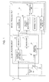
- FIG. 1 is a diagram illustrating a configuration of a wireless communication apparatus as an embodiment according to the present invention.
- reference numerals 1, 2, 3 and 4 denote a wireless communication apparatus, an antenna, a radio frequency (RF) signal processing circuit, and a baseband (BB) signal processing circuit, respectively.
- RF radio frequency
- BB baseband
- the radio frequency signal processing circuit 3 and the baseband signal processing circuit 4 will be abbreviated by “an RF signal processing circuit 3 and "a BB signal processing circuit 4", respectively.
- a mobile communication apparatus which wirelessly communicates with a base station will be described as an embodiment of the wireless communication apparatus 1.
- this embodiment is not limited to the mobile communication apparatus.
- This embodiment is further applicable to other wireless communication apparatuses each enabling matching the impedance of an antenna with that of a communication unit by changing the impedance of a tuning unit.
- reference numerals 10, 11, 12, 13, 14 and 15 denote a modulator, a demodulator, a transmission/reception switching unit, a signal processing unit, a variable impedance device, and an impedance controller, respectively.
- a communication unit 50 includes the transmission/reception switching unit 12, the modulator 10, and the demodulator 11.
- reference numerals 20, 21 and 22 denote a reception intensity measurement unit, a comparison unit, and a switching signal generator, respectively.
- a halting unit 51 includes the reception intensity measurement unit 20, the comparison unit 21, and the switching signal generator 22.
- the communication unit 50 receives the radio signal via the antenna 2.
- the tuning unit 5 tunes the impedance of the antenna 2.
- the impedance controllerl5 controls the tuning unit 5 to match the impedance of the antenna 2 with the impedance of the communication unit 50.
- the halting unit 51 halts controlling the impedance of the antenna 2 in accordance with an intensity of the received radio signal.
- the wireless communication apparatus 1 is configured to include the antenna 2, the RF signal processing circuit 3, the BB signal processing circuit 4 and the tuning unit 5.
- the RF signal processing circuit 3 is configured to modulate baseband signals, inputted from the BB signal processing circuit 4, into radio-frequency signals, and further, demodulate received signals, received from the antenna 2, into baseband signals.
- the RF signal processing circuit 3 is configured to include the modulator 10, the demodulator 11, the transmission/reception switching unit 12 and the impedance controller 15.
- the modulator 10 is configured to modulate baseband signals, inputted from the BB signal processing circuit 4, into radio-frequency signals, and output the radio-frequency signals resulting from the modulation to the antenna 2 as transmitting signals.
- the demodulator 11 is configured to demodulate received signals, received from the antenna 2, into baseband signals, and output the baseband signals resulting from the demodulation to the BB signal processing circuit 4.
- the transmission/reception switching unit 12 is configured to perform switching of two connections, one being a connection from the modulator 10 to the antenna 2, the other one being a connection from the antenna 2 to the demodulator 11.
- the impedance controller 15 is configured to, by adjusting the impedance value of the variable impedance device 14 included in the tuning unit 5, which will be described below, match the impedance of the antenna 2 with that of the RF signal processing circuit 3.
- the impedance controller 15 is configured to change the impedance value of the variable impedance device 14 by supplying a control signal thereto, which causes the impedance value of the variable impedance device 14 to be changed. Processes of controlling the impedance value of the variable impedance device 14, which are performed by the impedance controller 15, will be described below.
- the BB signal processing circuit 4 is configured to perform processing on baseband signals which are to be modulated into radio-frequency signals by the RF signal processing circuit 3 and/or baseband signals which were demodulated from radio-frequency signals by the RF signal processing circuit 3.
- the BB signal processing circuit 4 is configured to include the signal processing unit 13, the reception intensity measurement unit 20, a comparison unit 21 and the switching signal generator 22.
- the BB signal processing circuit 4 may be configured to realize a portion of or the whole of the components denoted by reference numerals 13 and 20 to 22 by using dedicated hardware circuits.
- the BB signal processing circuit 4 may be configured to include a processor, and a memory component for storing therein programs to be executed by the processor. Further, by causing the processor to execute the programs, a portion of or the whole of processes allocated to the components denoted by reference numerals 13 and 20 to 22 may be executed.
- the BB signal processing circuit 4 may be configured to include programmable large scale integrations (LSIs), such as field programmable gate arrays (FPGAs).
- the FPGAs may be configured to execute a portion of or the whole of processes allocated to the components denoted by reference numerals 13 and 20 to 22.
- the signal processing unit 13 is configured to supply the modulator 10 included in the RF signal processing circuit 3 with baseband signals to be transmitted.
- the signal processing unit 13 is configured to receive baseband signals resulting from demodulation of received radio-frequency signals, the demodulation being performed by the demodulator 11, and perform processing on the received baseband signals in accordance with kinds and contents of signals to be handled by the wireless communication apparatus 1.
- the reception intensity measurement unit 20 is configured to measure the reception intensity P of received signals on the basis of baseband signals resulting from demodulation of received signals having been received via the antenna 2.
- the reception intensity measurement unit 20 may be configured to, as the reception intensity P, measure interference signal power included in the baseband signals outputted from the demodulator 11.
- the comparison unit 21 is configured to compare the reception intensity P, having been measured by the reception intensity measurement unit 20, and a certain reference value R.
- the switching signal generator 22 is configured to generate switching signals on the basis of comparison results outputted from the comparison unit 21.
- the switching signal generator 22 is configured to, in the case where the reception intensity P is larger than the reference value R (i.e., P > R), generate a switching signal having a value "OFF".
- the switching signal generator 22 is configured to, in the case where the reception intensity P is less than or equal to the reference value R (i.e., P ⁇ R), generate a switching signal having a value "ON".
- the switching signal generator 22 is configured to output the switching signals to the impedance controllers 15.
- the impedance controller 15 is configured to halt processes of adjusting the impedance value of the variable impedance device 14 during a period of time while being supplied with the switching signal having a value "OFF".
- the impedance controller 15 is configured to be allowed to perform adjustment of the impedance value of the variable impedance device 14 during a period of time while being supplied with the switching signal having values other than the value "OFF" (for example, during a period of time while being supplied with the switching signal having the value "ON").
- the comparison unit 21 and the switching signal generator 22 are components corresponding to those of an example of a halting means according to an aspect of an embodiment of the present invention.
- the tuning unit 5 is configured to match the impedance of the antenna 2 with that of the RF signal processing circuit 3.
- the tuning unit 5 is configured to include the variable impedance device 14 therein.
- the variable impedance device 14 is configured to change the amount of capacitance and/or inductance included therein in accordance with a control signal supplied from the impedance controller 15.
- variable impedance device 14 may be configured to have a structure including a mechanical switch therein, such as a micro-electromechanical-systems (MEMS) based switch, and cause the mechanical switch to switch capacitors and coils connected to the antenna 2.
- MEMS micro-electromechanical-systems
- the variable impedance device 14 may be a MEMS based variable capacitor component, which enables changing the amount of capacitance thereof in conjunction with the variation of a distance between electrodes formed on the tips of built-in components each having a micro-movable structure, the variation of a distance between the electrodes resulting from causing the positions of the electrodes to be mechanically varied in accordance with an electrical signal supplied thereto.
- the variable impedance device 14 may be a varactor diode.
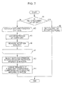
- FIG. 2 is a diagram illustrating an example of adjustment processes performed by the impedance controller 15.
- each of operations AA to AH which will be described below, may be a step.
- the impedance controller 15 determines whether the value of the switching signal received from the switching signal generator 22 is "ON” or "OFF". In the case where it is determined that the value of the switching signal is "OFF" (operation AA: OFF), the impedance controller 15 moves the processing to operation AB. During a period of time while the value of the switching signal remains to be "OFF", the impedance controller 15 halts the processes of adjusting the impedance value of the variable impedance device 14 (operation AB).
- the impedance controller 15 may cause the control signal, which is supplied to the variable impedance device 14, to be in a halt condition.
- the control signal is a voltage signal
- the impedance controller 15 makes the level of the voltage signal, which is supplied to the variable impedance device 14, to be "0". Subsequent thereto, the impedance controller 15 terminates the processing.
- the impedance controller 15 moves the processing to operation AC.
- the impedance controllers 15 performs operations AC to AF for each of predetermined matching conditions, the number of which is "n", each of the predetermined conditions being denoted by Ci ("i" is an integer number from 1 to "n").
- the impedance controller 15 performs control by supplying a control signal to the variable impedance device 14 so that the impedance value of the variable impedance device 14 comes to a target value corresponding to each of the matching condition Ci.
- the impedance controller 15 measures received signal power regarding received signals having been received via the antenna 2.
- the impedance controller 15 selects a matching condition, in which a maximum received signal power was measured, from among the matching conditions C1 to Cn.
- the impedance controller 15 performs control of the impedance value of the variable impedance device 14 so that the impedance value of the variable impedance device 14 comes to a target value corresponding to the matching condition having been selected in operation AG.
- the above-described control processes enable the impedance controller 15 to, in accordance with variation of the impedance of the antenna 2, perform adjustment of the impedance value of the variable impedance device 14 so as to maximize the gain of the antenna 2. That is, the above-described control processes enable the impedance controller 15 to, in accordance with variation of the impedance of the antenna 2, match impedances between the antenna 2 and the RF signal processing circuit 3.
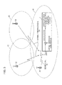
- FIG. 3 is a diagram illustrating interference signal power added to the power of received signals.
- a reference numeral 31 denotes an opposing communication apparatus which is currently expected to wirelessly communicate with the wireless communication apparatus 1.
- reference numerals 32 and 33 each are currently unexpected to communicate with the wireless communication apparatus 1.
- Reference numerals 41 to 43 are communication ranges within which wireless communication apparatuses are expected to wirelessly communicate with the corresponding communication apparatuses 31 to 33.
- the communication apparatuses 31 to 33 may be base stations. Further, the communication ranges 41 to 43 may be cell areas which are covered by the corresponding base stations 31 to 33. Since the wireless communication apparatus 1 is currently located within the cell area 41, the base station 31 is expected to communicate with the wireless communication apparatus 1.
- signals transmitting from the base station 31 and receiving at the wireless communication apparatus 1 are desired signals.
- the signal power of desired signals, transmitting from the base station 31, receiving at the wireless communication apparatus 1 and inputting to the antenna 2 is denoted by "S".
- S the signal power of desired signals, transmitting from the base station 31, receiving at the wireless communication apparatus 1 and inputting to the antenna 2
- G ⁇ S a value resulting from multiplying the signal power S by a gain G of the antenna 2, i.e., G ⁇ S, will be sometimes called “desired signal power”.
- signals, transmitting from the base stations 32 and 33 other than the base station 31 covering the cell 41, and receiving at the wireless communication apparatus 1 are external interference signals.
- the total amount of the signal power of the external interference signals, transmitting from base stations other than the base station 31, receiving at the wireless communication apparatus 1 and inputting to the antenna 2 are denoted by °'I1'°.
- a value resulting from multiplying the signal power I1 by the gain G of the antenna 2, i.e., G ⁇ I1 will be sometimes called "external interference signal power".
- the internal interference signals occurring inside the wireless communication apparatus 1 are added to received signals having been received by the wireless communication apparatus 1.
- the internal interference signals include therein, for example, thermal noise signals, noise signals occurring in amplifiers and the like.
- SIR signal-to-interference ratio
- the SIR is approximately equal to the vale of S/I1. That is, in the case where the value of the external interference signal power (G ⁇ I1) is larger than the reference value R, which is sufficiently larger than the value of the internal interference signal power I2, i.e., R >> I2, the SIR is approximately equal to the value of S/I1.
- the transmission quality is not affected by the gain G of the antenna 2. In such a case, it is unnecessary to perform processes of adjusting the impedance value of the variable impedance device 14 so as to match the impedance of the antenna 2 with that of the RF signal processing circuit 3.
- the halting unit 51 halts controlling the impedance of the antenna 2 in accordance with the comparative result of the internal interference signal power and the external interference signal power.
- the external interference signal power (G ⁇ I1) and the reference value R it is possible to determine whether it is necessary to perform processes of adjusting the impedance value of the variable impedance device 14, or not.
- the interference signal power (G ⁇ Il + I2) and the reference value R it is also possible to determine whether it is necessary to perform processes of adjusting the impedance value of the variable impedance device 14, or not.
- the wireless communication apparatus 1 is a mobile communication apparatus
- the wireless communication apparatus 1 is located under the environment where electric waves do not reach to a sufficient extent, such as underground shopping areas and suburbs far from base stations
- FIG. 4 is a diagram illustrating processes performed in an impedance control method according to an embodiment of the present invention.
- each of operations BA to BD which will be described below, may be a step.
- the reception intensity measurement unit 20 measures the reception intensity P of baseband signals resulting from demodulation of received signals and being inputted to the BB signal processing circuit 4.
- the reception intensity measurement unit 20 may measure, for example, the interference signal power (G ⁇ I1 + I2) as the reception intensity P.
- FIG. 5 is a diagram illustrating an example of an interference signal power measurement method according to an embodiment of the present invention.
- the reception intensity measurement unit 20 measures a reception intensity of a baseband pilot signal at each of predetermined dock times, and calculates a mean value V av from reception intensities of the baseband pilot signal, resulting from measurements performed at a plurality of times.
- the reception intensity measurement unit 20 calculates a square mean error value between respective measurement values and the mean value V av as the interference signal power.
- the comparison unit 21 compares the reception intensity P, which is measured by the reception intensity measurement unit 20, and the reference value R.
- the symbol k represents the Boltzmann constant
- the symbols B and T represent a received-signal frequency bandwidth of the wireless communication apparatus 1 and an absolute temperature, respectively.
- a value resulting from calculation using the formula (1) in accordance with a current temperature may be used as the reference value R.
- the reference value R may be calculated by using this formula (2) and a value resulting from measurement of internal interference signal power included in output signals from the RF signal processing circuit 3, the value being regarded as the internal interference signal power I2 of the wireless communication apparatus.
- the switching signal generator 22 outputs a switching signal having a value "OFF" to the impedance controller 15.
- operation BB in the case where it is determined that the reception intensity P is less than or equal to the reference value R (operation BB: N), the switching signal generator 22 outputs a switching signal having a value "ON" to the impedance controller 15.
- the halting unit 51 restarts controlling the impedance of the antenna 2 in accordance with the reception intensity of the received radio signal after the halting unit 51 halts controlling the impedance of the antenna 2. Subsequent thereto, the processing is terminated.
- the processes of adjusting the impedance value of the tuning unit 5 is halted. Therefore, the number of changing the impedance value of the tuning unit 5 is reduced. Furthermore, this reduction of the number of changing the impedance value of the tuning unit 5 results in delaying of the degradation of the variable impedance device 14.
- halting the processes of adjusting the impedance value, performed by the impedance controller 15 in operations AC to AH shown in FIG. 2 enables saving of electric power consumed in the processes of the adjustment. Further, halting the processes of adjusting the impedance value, performed by the impedance controller 15 in operations AC to AH shown in FIG. 2 , enables saving of electric power consumed in the processes of the adjustment. Moreover, while halting the process of controlling the impedance value of the variable impedance device 14, causing the control signal, which is supplied to the variable impedance device 14 by the impedance controller 15, to be in a halt condition enables saving of electric power consumed in driving the variable impedance device 14.
- the reception intensity measurement unit 20 measures the interference signal power (G ⁇ I1 + I2) as the reception intensity P, and in the case where the measured interference signal power (G ⁇ I1 + I2) is larger than the reference value R, the switching signal generator 22 outputs a switching signal having a value "OFF".
- the reception intensity measurement unit 20 may be configured to measure the desired signal power (G ⁇ S) as the reception intensity P. Further, the switching signal generator 22 may be configured to output a switching signal having a value "OFF" in the case where the desired signal power (G ⁇ S) is larger than the reference value R.
- the received signal power intensity measurement unit 20 may calculate, for example, the mean value of the reception intensities V av , which was described with reference to FIG. 5 , as the desired signal power (G ⁇ S).
- the SIR is not affected by the value of the gain G of the antenna 2. Therefore, from the total amount of the interference signal power (G ⁇ I1 + I2) and the desired signal power (G ⁇ S), that is, from the electric power of entire received signals inputted to the BB signal processing circuit 4, it is possible to determine whether the SIR is affected by the value of the gain G of the antenna 2, or not.
- the reception intensity measurement unit 20 may be configured to measure the electric power of entire received signals (G ⁇ I1 + I2 + G ⁇ S) as the reception intensity P.
- the switching signal generator 22 may be configured to output a switching signal having a value "OFF" in the case where the electric power (G ⁇ I1 + I2 + G ⁇ S) is larger than a certain reference value R.
- a certain reference value R employed in an embodiment in which the desired signal power (G ⁇ S) is used as the reception intensity P, as well as a certain reference value R employed in an embodiment in which the power of entire received signals (G ⁇ I1 + I2 + G ⁇ S) is used as the reception intensity P, may be also determined in accordance with the measured value of the internal inference signal power I2 of the wireless communication apparatus 1.
- the reception intensity measurement unit 20 measures the value of electric power as the reception intensity P. Further, the switching signal generator 22 determines the value of the switching signal on the basis of the result of comparison of the value of electric power and a certain reference value R.
- the halting unit 51 halts controlling the impedance of the antenna 2 when the intensity of the received radio signal is greater than a predetermined value set in accordance with a noise figure NF and a thermal noise X of the communication unit 50.
- the reception intensity measurement unit 20 may measure the reception intensity P which is expressed in the form of one of various kinds of indexes enabling expression of the intensities of the interference signals, the intensity of the desired signal and the intensity of the entire received signals.
- the reception intensity measurement unit 20 may determine the value of the switching signal on the basis of the result of comparison between the value of the reception intensity P and a certain reference value R, which are expressed in the form of one of the various kinds of indexes.
Landscapes
- Engineering & Computer Science (AREA)
- Computer Networks & Wireless Communication (AREA)
- Signal Processing (AREA)
- Transceivers (AREA)
- Input Circuits Of Receivers And Coupling Of Receivers And Audio Equipment (AREA)
- Details Of Aerials (AREA)
Abstract
Description
- The embodiments discussed herein are related to a wireless communication apparatus.
- Typical wireless communication apparatuses each include therein a tuning unit configured to match the impedance of an antenna thereof with that of a communication unit thereof. Further, a method, in which such a tuning unit includes a variable impedance device therein, and changing the impedance value of the variable impedance device in accordance with the variation of the impedance of the antenna enables matching the impedance of the antenna and that of the communication unit, is well known to those skilled in the art.
- In addition, technologies, which allow a mobile wireless terminal device to include an antenna tuning unit configured to perform impedance matching for all frequencies of receiving and transmitting radio signals, an antenna matching circuit control unit configured to include a variable amount of capacitance therein and perform impedance matching control on the antenna impedance of an antenna, and a controller configured to compare the level of a reception electric field of signals inputted to the mobile wireless terminal device and the level of a reception electric field of signals received at a base station communicating with the mobile wireless terminal device, and on the basis of this comparison result, perform impedance matching control on the antenna impedance by changing the amount of capacitance included in the antenna matching circuit control unit so that the antenna impedance can be optimal for a frequency of either the reception electric field of signals inputted to the mobile wireless communication terminal or the reception electric field of signals received at the base station communicating with the mobile wireless terminal device, whichever is lower in level, are well known to those skilled in the art (refer to Japanese Laid-open Patent Publication No.
2002-118488 - Further, a system and a method, which arbitrarily increase antenna efficiency in a transmitting frequency or a receiving frequency on the basis of a fading condition, an environmental condition, a non-ideal antenna efficiency balance, a mobile station forward versus reverse link usage condition, and a system forward versus reverse link usage condition, are well known to those skilled in the art (refer to Japanese Laid-open Patent Publication No.
2008-530957 - Frequent operations of changing the impedance value of a variable impedance device included in a matching device are likely to advance degradation of the variable impedance device. Further, performing processes of controlling the impedance value of a variable impedance device included in a matching device leads to increasing of electric power consumption.
- Accordingly, it is desirable in one aspect of the embodiment to, in a wireless communication apparatus and an impedance control method thereof, which enable matching the impedance of an antenna with that of a communication unit by changing the impedance value of a tuning unit, provide an embodiment of the wireless communication apparatus and the impedance control method thereof, which further enables reducing the number of changing the impedance value of the tuning unit.
- According to an aspect of the embodiment, a wireless communication apparatus includes: an antenna; a communication unit for receiving a radio signal via the antenna; a tuning unit for tuning an impedance of the antenna; an impedance controller for controlling the tuning unit to match the impedance of the antenna with an impedance of the communication unit; and a halting unit for halting controlling the impedance of the antenna in accordance with an intensity of the received radio signal.
-
-
FIG. 1 is a diagram illustrating a configuration of a wireless communication apparatus according to an embodiment of the present invention; -
FIG. 2 is a diagram illustrating an example of adjustment processes performed by an impedance controller according to an embodiment of the present invention; -
FIG. 3 is a diagram illustrating interference signal power added to electric power of received signals; -
FIG. 4 is a diagram illustrating processes performed in an impedance control method according to an embodiment of the present invention; and -
FIG. 5 is a diagram illustrating an example of an interference signal power measurement method according to an embodiment of the present invention. - Hereinafter, an embodiment according to the present invention will be described with reference to accompanying drawings.
FIG. 1 is a diagram illustrating a configuration of a wireless communication apparatus as an embodiment according to the present invention. InFIG. 1 ,reference numerals signal processing circuit 3 and the basebandsignal processing circuit 4 will be abbreviated by "an RFsignal processing circuit 3 and "a BBsignal processing circuit 4", respectively. - In the following explanation of this embodiment, a mobile communication apparatus which wirelessly communicates with a base station will be described as an embodiment of the
wireless communication apparatus 1. However, this embodiment is not limited to the mobile communication apparatus. This embodiment is further applicable to other wireless communication apparatuses each enabling matching the impedance of an antenna with that of a communication unit by changing the impedance of a tuning unit. - In
FIG. 1 ,reference numerals communication unit 50 includes the transmission/reception switching unit 12, themodulator 10, and thedemodulator 11. - Further,
reference numerals halting unit 51 includes the receptionintensity measurement unit 20, thecomparison unit 21, and theswitching signal generator 22. - The
communication unit 50 receives the radio signal via theantenna 2. The tuning unit 5 tunes the impedance of theantenna 2. The impedance controllerl5 controls the tuning unit 5 to match the impedance of theantenna 2 with the impedance of thecommunication unit 50. The haltingunit 51 halts controlling the impedance of theantenna 2 in accordance with an intensity of the received radio signal. - The
wireless communication apparatus 1 is configured to include theantenna 2, the RFsignal processing circuit 3, the BBsignal processing circuit 4 and the tuning unit 5. The RFsignal processing circuit 3 is configured to modulate baseband signals, inputted from the BBsignal processing circuit 4, into radio-frequency signals, and further, demodulate received signals, received from theantenna 2, into baseband signals. - The RF
signal processing circuit 3 is configured to include themodulator 10, thedemodulator 11, the transmission/reception switching unit 12 and theimpedance controller 15. Themodulator 10 is configured to modulate baseband signals, inputted from the BBsignal processing circuit 4, into radio-frequency signals, and output the radio-frequency signals resulting from the modulation to theantenna 2 as transmitting signals. Thedemodulator 11 is configured to demodulate received signals, received from theantenna 2, into baseband signals, and output the baseband signals resulting from the demodulation to the BBsignal processing circuit 4. The transmission/reception switching unit 12 is configured to perform switching of two connections, one being a connection from themodulator 10 to theantenna 2, the other one being a connection from theantenna 2 to thedemodulator 11. - The
impedance controller 15 is configured to, by adjusting the impedance value of thevariable impedance device 14 included in the tuning unit 5, which will be described below, match the impedance of theantenna 2 with that of the RFsignal processing circuit 3. Theimpedance controller 15 is configured to change the impedance value of thevariable impedance device 14 by supplying a control signal thereto, which causes the impedance value of thevariable impedance device 14 to be changed. Processes of controlling the impedance value of thevariable impedance device 14, which are performed by theimpedance controller 15, will be described below. - The BB
signal processing circuit 4 is configured to perform processing on baseband signals which are to be modulated into radio-frequency signals by the RFsignal processing circuit 3 and/or baseband signals which were demodulated from radio-frequency signals by the RFsignal processing circuit 3. The BBsignal processing circuit 4 is configured to include thesignal processing unit 13, the receptionintensity measurement unit 20, acomparison unit 21 and theswitching signal generator 22. - The BB
signal processing circuit 4 may be configured to realize a portion of or the whole of the components denoted byreference numerals signal processing circuit 4 may be configured to include a processor, and a memory component for storing therein programs to be executed by the processor. Further, by causing the processor to execute the programs, a portion of or the whole of processes allocated to the components denoted byreference numerals signal processing circuit 4 may be configured to include programmable large scale integrations (LSIs), such as field programmable gate arrays (FPGAs). The FPGAs may be configured to execute a portion of or the whole of processes allocated to the components denoted byreference numerals - The
signal processing unit 13 is configured to supply themodulator 10 included in the RFsignal processing circuit 3 with baseband signals to be transmitted. Thesignal processing unit 13 is configured to receive baseband signals resulting from demodulation of received radio-frequency signals, the demodulation being performed by thedemodulator 11, and perform processing on the received baseband signals in accordance with kinds and contents of signals to be handled by thewireless communication apparatus 1. - The reception
intensity measurement unit 20 is configured to measure the reception intensity P of received signals on the basis of baseband signals resulting from demodulation of received signals having been received via theantenna 2. For example, the receptionintensity measurement unit 20 may be configured to, as the reception intensity P, measure interference signal power included in the baseband signals outputted from thedemodulator 11. - The
comparison unit 21 is configured to compare the reception intensity P, having been measured by the receptionintensity measurement unit 20, and a certain reference value R. Theswitching signal generator 22 is configured to generate switching signals on the basis of comparison results outputted from thecomparison unit 21. Theswitching signal generator 22 is configured to, in the case where the reception intensity P is larger than the reference value R (i.e., P > R), generate a switching signal having a value "OFF". In contrast, theswitching signal generator 22 is configured to, in the case where the reception intensity P is less than or equal to the reference value R (i.e., P ≤ R), generate a switching signal having a value "ON". Theswitching signal generator 22 is configured to output the switching signals to theimpedance controllers 15. - The
impedance controller 15 is configured to halt processes of adjusting the impedance value of thevariable impedance device 14 during a period of time while being supplied with the switching signal having a value "OFF". Theimpedance controller 15 is configured to be allowed to perform adjustment of the impedance value of thevariable impedance device 14 during a period of time while being supplied with the switching signal having values other than the value "OFF" (for example, during a period of time while being supplied with the switching signal having the value "ON"). Thecomparison unit 21 and theswitching signal generator 22 are components corresponding to those of an example of a halting means according to an aspect of an embodiment of the present invention. - The tuning unit 5 is configured to match the impedance of the
antenna 2 with that of the RFsignal processing circuit 3. The tuning unit 5 is configured to include thevariable impedance device 14 therein. Thevariable impedance device 14 is configured to change the amount of capacitance and/or inductance included therein in accordance with a control signal supplied from theimpedance controller 15. - For example, the
variable impedance device 14 may be configured to have a structure including a mechanical switch therein, such as a micro-electromechanical-systems (MEMS) based switch, and cause the mechanical switch to switch capacitors and coils connected to theantenna 2. Further, for example, thevariable impedance device 14 may be a MEMS based variable capacitor component, which enables changing the amount of capacitance thereof in conjunction with the variation of a distance between electrodes formed on the tips of built-in components each having a micro-movable structure, the variation of a distance between the electrodes resulting from causing the positions of the electrodes to be mechanically varied in accordance with an electrical signal supplied thereto. Further, for example, thevariable impedance device 14 may be a varactor diode. - Next, processes of adjusting the impedance value of the
variable impedance device 14, which are performed by theimpedance controller 15, will be described below.FIG. 2 is a diagram illustrating an example of adjustment processes performed by theimpedance controller 15. In addition, in another aspect of an embodiment of the present invention, each of operations AA to AH, which will be described below, may be a step. - In operation AA, the
impedance controller 15 determines whether the value of the switching signal received from theswitching signal generator 22 is "ON" or "OFF". In the case where it is determined that the value of the switching signal is "OFF" (operation AA: OFF), theimpedance controller 15 moves the processing to operation AB. During a period of time while the value of the switching signal remains to be "OFF", theimpedance controller 15 halts the processes of adjusting the impedance value of the variable impedance device 14 (operation AB). - While halting the processes of adjusting the impedance value of the
variable impedance device 14, theimpedance controller 15 may cause the control signal, which is supplied to thevariable impedance device 14, to be in a halt condition. For example, in the case where the control signal is a voltage signal, theimpedance controller 15 makes the level of the voltage signal, which is supplied to thevariable impedance device 14, to be "0". Subsequent thereto, theimpedance controller 15 terminates the processing. - In the case where it is determined in operation AA that the value of the switching signal is "ON" (operation AA: ON), the
impedance controller 15 moves the processing to operation AC. Theimpedance controllers 15 performs operations AC to AF for each of predetermined matching conditions, the number of which is "n", each of the predetermined conditions being denoted by Ci ("i" is an integer number from 1 to "n"). - In operation AD, the
impedance controller 15 performs control by supplying a control signal to thevariable impedance device 14 so that the impedance value of thevariable impedance device 14 comes to a target value corresponding to each of the matching condition Ci. In operation AE, for each of the matching condition Ci, theimpedance controller 15 measures received signal power regarding received signals having been received via theantenna 2. - In operation AG, the
impedance controller 15 selects a matching condition, in which a maximum received signal power was measured, from among the matching conditions C1 to Cn. In operation AH, theimpedance controller 15 performs control of the impedance value of thevariable impedance device 14 so that the impedance value of thevariable impedance device 14 comes to a target value corresponding to the matching condition having been selected in operation AG. - The above-described control processes enable the
impedance controller 15 to, in accordance with variation of the impedance of theantenna 2, perform adjustment of the impedance value of thevariable impedance device 14 so as to maximize the gain of theantenna 2. That is, the above-described control processes enable theimpedance controller 15 to, in accordance with variation of the impedance of theantenna 2, match impedances between theantenna 2 and the RFsignal processing circuit 3. - Next, interference signal power, which is added to the power of signals received by the
wireless communication apparatus 1, will be described below.FIG. 3 is a diagram illustrating interference signal power added to the power of received signals. InFIG. 3 , a reference numeral 31 denotes an opposing communication apparatus which is currently expected to wirelessly communicate with thewireless communication apparatus 1. Further,reference numerals wireless communication apparatus 1.Reference numerals 41 to 43 are communication ranges within which wireless communication apparatuses are expected to wirelessly communicate with the corresponding communication apparatuses 31 to 33. - In the case where the
wireless communication apparatus 1 is, for example, a mobile communication apparatus, the communication apparatuses 31 to 33 may be base stations. Further, the communication ranges 41 to 43 may be cell areas which are covered by the corresponding base stations 31 to 33. Since thewireless communication apparatus 1 is currently located within thecell area 41, the base station 31 is expected to communicate with thewireless communication apparatus 1. - Therefore, signals transmitting from the base station 31 and receiving at the
wireless communication apparatus 1 are desired signals. Here, the signal power of desired signals, transmitting from the base station 31, receiving at thewireless communication apparatus 1 and inputting to theantenna 2, is denoted by "S". In the following description, a value resulting from multiplying the signal power S by a gain G of theantenna 2, i.e., G × S, will be sometimes called "desired signal power". - Meanwhile, signals, transmitting from the
base stations cell 41, and receiving at thewireless communication apparatus 1, are external interference signals. Here, the total amount of the signal power of the external interference signals, transmitting from base stations other than the base station 31, receiving at thewireless communication apparatus 1 and inputting to theantenna 2, are denoted by °'I1'°. In the following description, a value resulting from multiplying the signal power I1 by the gain G of theantenna 2, i.e., G × I1, will be sometimes called "external interference signal power". - Further, internal interference signals occurring inside the
wireless communication apparatus 1 are added to received signals having been received by thewireless communication apparatus 1. The internal interference signals include therein, for example, thermal noise signals, noise signals occurring in amplifiers and the like. The signal power of the internal interference signals is denoted by "internal interference signal power I2'°. Therefore, the total amount of signal power of received signals having been received by thewireless communication apparatus 1, i.e., Pall, is given by the following formula: Pall = G × S + G × I1 + I2. In the following description, the total amount of the signal power resulting from adding the internal interference signal power I2 to the external inference signal power (G × I1) will be sometimes called "interference signal power". - Meanwhile, transmission quality of a transmission link between the
wireless communication apparatus 1 and the base station 31 can be verified by using a signal-to-interference ratio (SIR). This SIR can be calculated by using the following formula: SIR = (G × S) / (G × I1 + I2). - According to the above-described formula for calculating the SIR, in the case where the value of the external interference signal power (G × I1) is sufficiently large for the value of the internal interference signal power I2 to be ignored, it can be understood that the SIR is approximately equal to the vale of S/I1. That is, in the case where the value of the external interference signal power (G × I1) is larger than the reference value R, which is sufficiently larger than the value of the internal interference signal power I2, i.e., R >> I2, the SIR is approximately equal to the value of S/I1. As a result, in the case where the value of the external interference signal power (G × I1) is larger than the reference value R, the transmission quality is not affected by the gain G of the
antenna 2. In such a case, it is unnecessary to perform processes of adjusting the impedance value of thevariable impedance device 14 so as to match the impedance of theantenna 2 with that of the RFsignal processing circuit 3. - The halting
unit 51 halts controlling the impedance of theantenna 2 in accordance with the comparative result of the internal interference signal power and the external interference signal power. In this embodiment, by comparing the external interference signal power (G × I1) and the reference value R, it is possible to determine whether it is necessary to perform processes of adjusting the impedance value of thevariable impedance device 14, or not. Further, in the case where a value sufficiently larger than the internal interference signal power I2 is selected as the reference value R, by comparing the interference signal power (G × Il + I2) and the reference value R, it is also possible to determine whether it is necessary to perform processes of adjusting the impedance value of thevariable impedance device 14, or not. - For example, in the case where the
wireless communication apparatus 1 is a mobile communication apparatus, except for the case where thewireless communication apparatus 1 is located under the environment where electric waves do not reach to a sufficient extent, such as underground shopping areas and suburbs far from base stations, there are lots of cases where a condition expressed by the following formula: Interference signal power (G × I1 + I2) > Reference value R >> Internal interference signal power I2, is satisfied, and thus, the processes of adjusting the impedance value of thevariable impedance device 14 is likely to be unnecessary. - Accordingly, in the case where the interference signal power (G × I1 + I2) is larger than the reference value R, the
switching signal generator 22 shown inFIG. 1 outputs a switching signal having a value "OFF", and thereby, causes theimpedance controller 15 to halt the processes of adjusting the impedance value of thevariable impedance device 14.FIG. 4 is a diagram illustrating processes performed in an impedance control method according to an embodiment of the present invention. In addition, in another aspect of an embodiment of the present invention, each of operations BA to BD, which will be described below, may be a step. - In operation BA, the reception
intensity measurement unit 20 measures the reception intensity P of baseband signals resulting from demodulation of received signals and being inputted to the BBsignal processing circuit 4. The receptionintensity measurement unit 20 may measure, for example, the interference signal power (G × I1 + I2) as the reception intensity P. -
FIG. 5 is a diagram illustrating an example of an interference signal power measurement method according to an embodiment of the present invention. The receptionintensity measurement unit 20 measures a reception intensity of a baseband pilot signal at each of predetermined dock times, and calculates a mean value Vav from reception intensities of the baseband pilot signal, resulting from measurements performed at a plurality of times. The receptionintensity measurement unit 20 calculates a square mean error value between respective measurement values and the mean value Vav as the interference signal power. - In operation BB shown in
FIG. 4 , thecomparison unit 21 compares the reception intensity P, which is measured by the receptionintensity measurement unit 20, and the reference value R. The reference value R may be determined in accordance with a noise figure NF and thermal noise X (= kBT) of thewireless communication apparatus 1. In addition, the symbol k represents the Boltzmann constant, and the symbols B and T represent a received-signal frequency bandwidth of thewireless communication apparatus 1 and an absolute temperature, respectively. - For example, the reference value R may be determined in advance by using the following formula (1) resulting from summation of a noise figure NF of the RF
signal processing circuit 3, which is pre-planned in designing thereof, a thermal noise X in the case where the wireless communication apparatus is used at a rated temperature, and a predetermined margin M (for example, M = 5 [dB]) -

- Further, a value resulting from calculation using the formula (1) in accordance with a current temperature may be used as the reference value R.
- Alternatively, when the
wireless communication apparatuses 1 are shipped, for each individual of thewireless communication apparatus 1 or each of extracted samples of thewireless communication apparatus 1, the internal interference signal power I2 of thewireless communication apparatus 1 is measured. Further thereto, the reference value R may be determined in advance by using the following formula (2) resulting from summation of this measured value I2 and a predetermined margin M (for example, M = 5 [dB]). -

- The reference value R may be calculated by using this formula (2) and a value resulting from measurement of internal interference signal power included in output signals from the RF
signal processing circuit 3, the value being regarded as the internal interference signal power I2 of the wireless communication apparatus. - In operation BB, in the case where it is determined that the reception intensity P is larger than the reference value R (operation BB: Y), that is, the following determination formula (3):
-

- is satisfied, the
switching signal generator 22 outputs a switching signal having a value "OFF" to theimpedance controller 15. In contrast, in operation BB, in the case where it is determined that the reception intensity P is less than or equal to the reference value R (operation BB: N), theswitching signal generator 22 outputs a switching signal having a value "ON" to theimpedance controller 15. Thus, the haltingunit 51 restarts controlling the impedance of theantenna 2 in accordance with the reception intensity of the received radio signal after the haltingunit 51 halts controlling the impedance of theantenna 2. Subsequent thereto, the processing is terminated. - According to the above-described embodiment, during a period of time while the SIR is not affected by the value of the gain G of the
antenna 2, that is, during a period of time while the SIR is not affected by whether the impedances of theantenna 2 and the RFsignal processing circuit 3 are sufficiently matched with each other, or not, the processes of adjusting the impedance value of the tuning unit 5 is halted. Therefore, the number of changing the impedance value of the tuning unit 5 is reduced. Furthermore, this reduction of the number of changing the impedance value of the tuning unit 5 results in delaying of the degradation of thevariable impedance device 14. - Moreover, halting the processes of adjusting the impedance value, performed by the
impedance controller 15 in operations AC to AH shown inFIG. 2 , enables saving of electric power consumed in the processes of the adjustment. Further, halting the processes of adjusting the impedance value, performed by theimpedance controller 15 in operations AC to AH shown inFIG. 2 , enables saving of electric power consumed in the processes of the adjustment. Moreover, while halting the process of controlling the impedance value of thevariable impedance device 14, causing the control signal, which is supplied to thevariable impedance device 14 by theimpedance controller 15, to be in a halt condition enables saving of electric power consumed in driving thevariable impedance device 14. - In addition, in the above-described embodiment, the reception
intensity measurement unit 20 measures the interference signal power (G × I1 + I2) as the reception intensity P, and in the case where the measured interference signal power (G × I1 + I2) is larger than the reference value R, theswitching signal generator 22 outputs a switching signal having a value "OFF". - The signal-to-interference ratio SIR is given by a formula: SIR = 1 / (I1 / S + I2 / (G × S)). Therefore, in the case where the value of the desired signal power (G × S) is sufficiently large for the internal interference signal power I2 to be ignored, the SIR is also approximately equal to S / I1. That is, in the case where the value of the desired signal power (G × S) is sufficiently large for the internal interference signal power I2 to be ignored, the SIR is not affected by the value of the gain G of the
antenna 2. - Therefore, in a different embodiment, the reception
intensity measurement unit 20 may be configured to measure the desired signal power (G × S) as the reception intensity P. Further, theswitching signal generator 22 may be configured to output a switching signal having a value "OFF" in the case where the desired signal power (G × S) is larger than the reference value R. The received signal powerintensity measurement unit 20 may calculate, for example, the mean value of the reception intensities Vav, which was described with reference toFIG. 5 , as the desired signal power (G × S). - As described above, in the case where the interference signal power (G × I1 + I2) is larger than a certain reference value, as well as in the case where the desired signal power (G × S) is larger than a certain reference value, the SIR is not affected by the value of the gain G of the
antenna 2. Therefore, from the total amount of the interference signal power (G × I1 + I2) and the desired signal power (G × S), that is, from the electric power of entire received signals inputted to the BBsignal processing circuit 4, it is possible to determine whether the SIR is affected by the value of the gain G of theantenna 2, or not. That is, by determining whether the electric power of entire received signals inputted to the BBsignal processing circuit 4, i.e., (G × I1 + I2 + G × S), is larger than a certain reference value, or not, it is possible to determine whether the SIR is affected by the value of the gain G of theantenna 2. - Therefore, in a different embodiment, the reception
intensity measurement unit 20 may be configured to measure the electric power of entire received signals (G × I1 + I2 + G × S) as the reception intensity P. Further, theswitching signal generator 22 may be configured to output a switching signal having a value "OFF" in the case where the electric power (G × I1 + I2 + G × S) is larger than a certain reference value R. - A certain reference value R employed in an embodiment in which the desired signal power (G × S) is used as the reception intensity P, as well as a certain reference value R employed in an embodiment in which the electric power of entire received signals (G × I1 + I2 + G × S) is used as the reception intensity P, may be also determined in accordance with a noise figure NF and thermal noise X (= kBT) of the
wireless communication apparatus 1. Further, a certain reference value R employed in an embodiment in which the desired signal power (G × S) is used as the reception intensity P, as well as a certain reference value R employed in an embodiment in which the power of entire received signals (G × I1 + I2 + G × S) is used as the reception intensity P, may be also determined in accordance with the measured value of the internal inference signal power I2 of thewireless communication apparatus 1. - Further, in the above-described embodiment, the reception
intensity measurement unit 20 measures the value of electric power as the reception intensity P. Further, theswitching signal generator 22 determines the value of the switching signal on the basis of the result of comparison of the value of electric power and a certain reference value R. The haltingunit 51 halts controlling the impedance of theantenna 2 when the intensity of the received radio signal is greater than a predetermined value set in accordance with a noise figure NF and a thermal noise X of thecommunication unit 50. - As a substitute for this method, the reception
intensity measurement unit 20 may measure the reception intensity P which is expressed in the form of one of various kinds of indexes enabling expression of the intensities of the interference signals, the intensity of the desired signal and the intensity of the entire received signals. The receptionintensity measurement unit 20 may determine the value of the switching signal on the basis of the result of comparison between the value of the reception intensity P and a certain reference value R, which are expressed in the form of one of the various kinds of indexes. In the case where the reception index P is expressed in the form of one of the various kinds of indexes, the corresponding reference value R used therein may be also determined in accordance with a noise figure NF and thermal noise X (= kBT) of thewireless communication apparatus 1, or the measured value of the internal interference signal power I2 of thewireless communication apparatus 1. - With respect to aspects of the present invention including the foregoing embodiments, the following appendixes will be further disclosed.
Claims (5)
- A wireless communication apparatus comprising:an antenna;a communication unit for receiving a radio signal via the antenna;a tuning unit for tuning an impedance of the antenna;an impedance controller for controlling the tuning unit to match the impedance of the antenna with an impedance of the communication unit; anda halting unit for halting controlling the impedance of the antenna in accordance with an intensity of the received radio signal.
- The wireless communication apparatus of claim 1, wherein the halting unit restarts controlling the impedance of the antenna in accordance with the reception intensity of the received radio signal after the halting unit halts controlling the impedance of the antenna.
- The wireless communication apparatus of claim 1, wherein the halting unit halts controlling the impedance of the antenna when the reception intensity of the received radio signal is greater than a predetermined value.
- The wireless communication apparatus of claim 3, wherein the predetermined value is set in accordance with a noise figure and a thermal noise of the communication unit.
- A method of controlling a tuning unit for tuning an impedance of an antenna to match with an impedance of a communication unit for receiving a radio signal, comprising:receiving the radio signal via the antenna; andhalting controlling the impedance of the antenna in accordance with an intensity of the received radio signal.
Applications Claiming Priority (1)
| Application Number | Priority Date | Filing Date | Title |
|---|---|---|---|
| JP2009148973A JP5310295B2 (en) | 2009-06-23 | 2009-06-23 | Wireless communication apparatus and impedance control method |
Publications (3)
| Publication Number | Publication Date |
|---|---|
| EP2273684A2 true EP2273684A2 (en) | 2011-01-12 |
| EP2273684A3 EP2273684A3 (en) | 2014-04-23 |
| EP2273684B1 EP2273684B1 (en) | 2015-09-09 |
Family
ID=42790812
Family Applications (1)
| Application Number | Title | Priority Date | Filing Date |
|---|---|---|---|
| EP10165906.8A Not-in-force EP2273684B1 (en) | 2009-06-23 | 2010-06-14 | Wireless communication apparatus |
Country Status (3)
| Country | Link |
|---|---|
| US (1) | US8285235B2 (en) |
| EP (1) | EP2273684B1 (en) |
| JP (1) | JP5310295B2 (en) |
Cited By (1)
| Publication number | Priority date | Publication date | Assignee | Title |
|---|---|---|---|---|
| EP3179635A4 (en) * | 2014-08-07 | 2018-04-11 | Panasonic Intellectual Property Management Co., Ltd. | Radio apparatus |
Families Citing this family (7)
| Publication number | Priority date | Publication date | Assignee | Title |
|---|---|---|---|---|
| JP5505242B2 (en) * | 2010-10-07 | 2014-05-28 | 富士通株式会社 | Communication apparatus and control method |
| JP5953525B2 (en) * | 2011-12-16 | 2016-07-20 | インテル・コーポレーション | Wireless communication device using time-varying antenna module |
| US20140065982A1 (en) | 2012-09-05 | 2014-03-06 | Seong-Youp Suh | Plug-and-play time-variant antenna module for wireless communication devices |
| EP2712021B1 (en) * | 2012-09-21 | 2018-04-04 | Siemens Aktiengesellschaft | Antenna for a read/write device for RFID assemblies and read/write device for operation with an external antenna |
| KR102166351B1 (en) * | 2014-01-29 | 2020-10-15 | 삼성전자주식회사 | Communication method and apparatus |
| JP6616584B2 (en) * | 2015-04-09 | 2019-12-04 | ルネサスエレクトロニクス株式会社 | Semiconductor device |
| CN114554020A (en) * | 2020-11-24 | 2022-05-27 | 西门子(深圳)磁共振有限公司 | Calling device of magnetic resonance imaging system and magnetic resonance imaging system |
Citations (2)
| Publication number | Priority date | Publication date | Assignee | Title |
|---|---|---|---|---|
| JP2002118488A (en) | 2000-10-06 | 2002-04-19 | Nec Saitama Ltd | Mobile radio terminal device |
| JP2008530957A (en) | 2005-02-17 | 2008-08-07 | 京セラ株式会社 | Antenna adjustment system and method in communication state of mobile station |
Family Cites Families (5)
| Publication number | Priority date | Publication date | Assignee | Title |
|---|---|---|---|---|
| JP2888179B2 (en) * | 1995-08-24 | 1999-05-10 | 日本電気株式会社 | Antenna tuning controller |
| JP4455973B2 (en) * | 2004-10-08 | 2010-04-21 | Okiセミコンダクタ株式会社 | Data receiving apparatus and threshold value determining method |
| JP2006186961A (en) * | 2004-12-02 | 2006-07-13 | Casio Comput Co Ltd | Receiving apparatus, circuit, and method |
| JP4922677B2 (en) * | 2005-07-01 | 2012-04-25 | パナソニック株式会社 | Wireless communication device |
| JP4729539B2 (en) * | 2007-08-10 | 2011-07-20 | トヨタ自動車株式会社 | Wireless receiver |
-
2009
- 2009-06-23 JP JP2009148973A patent/JP5310295B2/en not_active Expired - Fee Related
-
2010
- 2010-06-14 EP EP10165906.8A patent/EP2273684B1/en not_active Not-in-force
- 2010-06-17 US US12/817,781 patent/US8285235B2/en not_active Expired - Fee Related
Patent Citations (2)
| Publication number | Priority date | Publication date | Assignee | Title |
|---|---|---|---|---|
| JP2002118488A (en) | 2000-10-06 | 2002-04-19 | Nec Saitama Ltd | Mobile radio terminal device |
| JP2008530957A (en) | 2005-02-17 | 2008-08-07 | 京セラ株式会社 | Antenna adjustment system and method in communication state of mobile station |
Cited By (1)
| Publication number | Priority date | Publication date | Assignee | Title |
|---|---|---|---|---|
| EP3179635A4 (en) * | 2014-08-07 | 2018-04-11 | Panasonic Intellectual Property Management Co., Ltd. | Radio apparatus |
Also Published As
| Publication number | Publication date |
|---|---|
| EP2273684B1 (en) | 2015-09-09 |
| EP2273684A3 (en) | 2014-04-23 |
| JP2011009862A (en) | 2011-01-13 |
| US20100323650A1 (en) | 2010-12-23 |
| US8285235B2 (en) | 2012-10-09 |
| JP5310295B2 (en) | 2013-10-09 |
Similar Documents
| Publication | Publication Date | Title |
|---|---|---|
| EP2273684B1 (en) | Wireless communication apparatus | |
| US9698758B2 (en) | Methods for tuning an adaptive impedance matching network with a look-up table | |
| US8131232B2 (en) | Method and apparatus for antenna tuning | |
| EP3010291B1 (en) | Adaptive and power-controllable wifi adjusting method and device | |
| US20180083657A1 (en) | Method and apparatus for managing operations of a communication device | |
| EP3035446B1 (en) | Method and apparatus for tuning antennas in a communication device | |
| EP2557688B1 (en) | A controller for a radio circuit | |
| CN204068947U (en) | Adjustable mean frequency wireless receiver and bluetooth module | |
| EP3188309A1 (en) | Method and apparatus for tuning a communication device | |
| US20110269416A1 (en) | Transmitter | |
| US10333572B2 (en) | Antenna tuner control circuit, front-end circuit and communication device | |
| CN104954039B (en) | The impedance matching methods and system of antenna | |
| EP2847864B1 (en) | Apparatus and method for matching antenna impedance in wireless communication system | |
| Qaragoez et al. | Time Division Duplexing for Enhanced Simultaneous Wireless Information and Power Transfer via Backscattering | |
| EP3244541A1 (en) | Transmitter efficiency optimization | |
| CN105958204A (en) | Antenna parameter automatic adjusting method, antenna parameter automatic adjusting device, and antenna parameter automatic adjusting antenna | |
| CA2777137C (en) | Method and apparatus for managing operations of a communication device |
Legal Events
| Date | Code | Title | Description |
|---|---|---|---|
| PUAI | Public reference made under article 153(3) epc to a published international application that has entered the european phase |
Free format text: ORIGINAL CODE: 0009012 |
|
| AK | Designated contracting states |
Kind code of ref document: A2 Designated state(s): AL AT BE BG CH CY CZ DE DK EE ES FI FR GB GR HR HU IE IS IT LI LT LU LV MC MK MT NL NO PL PT RO SE SI SK SM TR |
|
| AX | Request for extension of the european patent |
Extension state: BA ME RS |
|
| PUAL | Search report despatched |
Free format text: ORIGINAL CODE: 0009013 |
|
| AK | Designated contracting states |
Kind code of ref document: A3 Designated state(s): AL AT BE BG CH CY CZ DE DK EE ES FI FR GB GR HR HU IE IS IT LI LT LU LV MC MK MT NL NO PL PT RO SE SI SK SM TR |
|
| AX | Request for extension of the european patent |
Extension state: BA ME RS |
|
| RIC1 | Information provided on ipc code assigned before grant |
Ipc: H04B 1/18 20060101AFI20140314BHEP Ipc: H04B 1/04 20060101ALI20140314BHEP |
|
| 17P | Request for examination filed |
Effective date: 20140716 |
|
| RBV | Designated contracting states (corrected) |
Designated state(s): AL AT BE BG CH CY CZ DE DK EE ES FI FR GB GR HR HU IE IS IT LI LT LU LV MC MK MT NL NO PL PT RO SE SI SK SM TR |
|
| GRAP | Despatch of communication of intention to grant a patent |
Free format text: ORIGINAL CODE: EPIDOSNIGR1 |
|
| INTG | Intention to grant announced |
Effective date: 20150429 |
|
| GRAS | Grant fee paid |
Free format text: ORIGINAL CODE: EPIDOSNIGR3 |
|
| GRAA | (expected) grant |
Free format text: ORIGINAL CODE: 0009210 |
|
| AK | Designated contracting states |
Kind code of ref document: B1 Designated state(s): AL AT BE BG CH CY CZ DE DK EE ES FI FR GB GR HR HU IE IS IT LI LT LU LV MC MK MT NL NO PL PT RO SE SI SK SM TR |
|
| REG | Reference to a national code |
Ref country code: GB Ref legal event code: FG4D |
|
| REG | Reference to a national code |
Ref country code: AT Ref legal event code: REF Ref document number: 748869 Country of ref document: AT Kind code of ref document: T Effective date: 20150915 Ref country code: CH Ref legal event code: EP |
|
| REG | Reference to a national code |
Ref country code: IE Ref legal event code: FG4D |
|
| REG | Reference to a national code |
Ref country code: DE Ref legal event code: R096 Ref document number: 602010027314 Country of ref document: DE |
|
| REG | Reference to a national code |
Ref country code: NL Ref legal event code: MP Effective date: 20150909 |
|
| PG25 | Lapsed in a contracting state [announced via postgrant information from national office to epo] |
Ref country code: FI Free format text: LAPSE BECAUSE OF FAILURE TO SUBMIT A TRANSLATION OF THE DESCRIPTION OR TO PAY THE FEE WITHIN THE PRESCRIBED TIME-LIMIT Effective date: 20150909 Ref country code: GR Free format text: LAPSE BECAUSE OF FAILURE TO SUBMIT A TRANSLATION OF THE DESCRIPTION OR TO PAY THE FEE WITHIN THE PRESCRIBED TIME-LIMIT Effective date: 20151210 Ref country code: NO Free format text: LAPSE BECAUSE OF FAILURE TO SUBMIT A TRANSLATION OF THE DESCRIPTION OR TO PAY THE FEE WITHIN THE PRESCRIBED TIME-LIMIT Effective date: 20151209 Ref country code: LV Free format text: LAPSE BECAUSE OF FAILURE TO SUBMIT A TRANSLATION OF THE DESCRIPTION OR TO PAY THE FEE WITHIN THE PRESCRIBED TIME-LIMIT Effective date: 20150909 Ref country code: LT Free format text: LAPSE BECAUSE OF FAILURE TO SUBMIT A TRANSLATION OF THE DESCRIPTION OR TO PAY THE FEE WITHIN THE PRESCRIBED TIME-LIMIT Effective date: 20150909 |
|
| REG | Reference to a national code |
Ref country code: LT Ref legal event code: MG4D |
|
| REG | Reference to a national code |
Ref country code: AT Ref legal event code: MK05 Ref document number: 748869 Country of ref document: AT Kind code of ref document: T Effective date: 20150909 |
|
| PG25 | Lapsed in a contracting state [announced via postgrant information from national office to epo] |
Ref country code: ES Free format text: LAPSE BECAUSE OF FAILURE TO SUBMIT A TRANSLATION OF THE DESCRIPTION OR TO PAY THE FEE WITHIN THE PRESCRIBED TIME-LIMIT Effective date: 20150909 Ref country code: SE Free format text: LAPSE BECAUSE OF FAILURE TO SUBMIT A TRANSLATION OF THE DESCRIPTION OR TO PAY THE FEE WITHIN THE PRESCRIBED TIME-LIMIT Effective date: 20150909 Ref country code: HR Free format text: LAPSE BECAUSE OF FAILURE TO SUBMIT A TRANSLATION OF THE DESCRIPTION OR TO PAY THE FEE WITHIN THE PRESCRIBED TIME-LIMIT Effective date: 20150909 |
|
| PG25 | Lapsed in a contracting state [announced via postgrant information from national office to epo] |
Ref country code: NL Free format text: LAPSE BECAUSE OF FAILURE TO SUBMIT A TRANSLATION OF THE DESCRIPTION OR TO PAY THE FEE WITHIN THE PRESCRIBED TIME-LIMIT Effective date: 20150909 |
|
| PG25 | Lapsed in a contracting state [announced via postgrant information from national office to epo] |
Ref country code: CZ Free format text: LAPSE BECAUSE OF FAILURE TO SUBMIT A TRANSLATION OF THE DESCRIPTION OR TO PAY THE FEE WITHIN THE PRESCRIBED TIME-LIMIT Effective date: 20150909 Ref country code: SK Free format text: LAPSE BECAUSE OF FAILURE TO SUBMIT A TRANSLATION OF THE DESCRIPTION OR TO PAY THE FEE WITHIN THE PRESCRIBED TIME-LIMIT Effective date: 20150909 Ref country code: IT Free format text: LAPSE BECAUSE OF FAILURE TO SUBMIT A TRANSLATION OF THE DESCRIPTION OR TO PAY THE FEE WITHIN THE PRESCRIBED TIME-LIMIT Effective date: 20150909 Ref country code: EE Free format text: LAPSE BECAUSE OF FAILURE TO SUBMIT A TRANSLATION OF THE DESCRIPTION OR TO PAY THE FEE WITHIN THE PRESCRIBED TIME-LIMIT Effective date: 20150909 Ref country code: IS Free format text: LAPSE BECAUSE OF FAILURE TO SUBMIT A TRANSLATION OF THE DESCRIPTION OR TO PAY THE FEE WITHIN THE PRESCRIBED TIME-LIMIT Effective date: 20160109 |
|
| PG25 | Lapsed in a contracting state [announced via postgrant information from national office to epo] |
Ref country code: PL Free format text: LAPSE BECAUSE OF FAILURE TO SUBMIT A TRANSLATION OF THE DESCRIPTION OR TO PAY THE FEE WITHIN THE PRESCRIBED TIME-LIMIT Effective date: 20150909 Ref country code: AT Free format text: LAPSE BECAUSE OF FAILURE TO SUBMIT A TRANSLATION OF THE DESCRIPTION OR TO PAY THE FEE WITHIN THE PRESCRIBED TIME-LIMIT Effective date: 20150909 Ref country code: RO Free format text: LAPSE BECAUSE OF FAILURE TO SUBMIT A TRANSLATION OF THE DESCRIPTION OR TO PAY THE FEE WITHIN THE PRESCRIBED TIME-LIMIT Effective date: 20150909 Ref country code: PT Free format text: LAPSE BECAUSE OF FAILURE TO SUBMIT A TRANSLATION OF THE DESCRIPTION OR TO PAY THE FEE WITHIN THE PRESCRIBED TIME-LIMIT Effective date: 20160111 |
|
| REG | Reference to a national code |
Ref country code: FR Ref legal event code: PLFP Year of fee payment: 7 |
|
| REG | Reference to a national code |
Ref country code: DE Ref legal event code: R097 Ref document number: 602010027314 Country of ref document: DE |
|
| PLBE | No opposition filed within time limit |
Free format text: ORIGINAL CODE: 0009261 |
|
| STAA | Information on the status of an ep patent application or granted ep patent |
Free format text: STATUS: NO OPPOSITION FILED WITHIN TIME LIMIT |
|
| 26N | No opposition filed |
Effective date: 20160610 |
|
| PG25 | Lapsed in a contracting state [announced via postgrant information from national office to epo] |
Ref country code: DK Free format text: LAPSE BECAUSE OF FAILURE TO SUBMIT A TRANSLATION OF THE DESCRIPTION OR TO PAY THE FEE WITHIN THE PRESCRIBED TIME-LIMIT Effective date: 20150909 Ref country code: SI Free format text: LAPSE BECAUSE OF FAILURE TO SUBMIT A TRANSLATION OF THE DESCRIPTION OR TO PAY THE FEE WITHIN THE PRESCRIBED TIME-LIMIT Effective date: 20150909 |
|
| PG25 | Lapsed in a contracting state [announced via postgrant information from national office to epo] |
Ref country code: BE Free format text: LAPSE BECAUSE OF FAILURE TO SUBMIT A TRANSLATION OF THE DESCRIPTION OR TO PAY THE FEE WITHIN THE PRESCRIBED TIME-LIMIT Effective date: 20150909 |
|
| PG25 | Lapsed in a contracting state [announced via postgrant information from national office to epo] |
Ref country code: MC Free format text: LAPSE BECAUSE OF FAILURE TO SUBMIT A TRANSLATION OF THE DESCRIPTION OR TO PAY THE FEE WITHIN THE PRESCRIBED TIME-LIMIT Effective date: 20150909 |
|
| REG | Reference to a national code |
Ref country code: CH Ref legal event code: PL |
|
| REG | Reference to a national code |
Ref country code: IE Ref legal event code: MM4A |
|
| PG25 | Lapsed in a contracting state [announced via postgrant information from national office to epo] |
Ref country code: LI Free format text: LAPSE BECAUSE OF NON-PAYMENT OF DUE FEES Effective date: 20160630 Ref country code: CH Free format text: LAPSE BECAUSE OF NON-PAYMENT OF DUE FEES Effective date: 20160630 |
|
| REG | Reference to a national code |
Ref country code: FR Ref legal event code: PLFP Year of fee payment: 8 |
|
| PG25 | Lapsed in a contracting state [announced via postgrant information from national office to epo] |
Ref country code: IE Free format text: LAPSE BECAUSE OF NON-PAYMENT OF DUE FEES Effective date: 20160614 |
|
| PGFP | Annual fee paid to national office [announced via postgrant information from national office to epo] |
Ref country code: GB Payment date: 20170614 Year of fee payment: 8 Ref country code: DE Payment date: 20170606 Year of fee payment: 8 Ref country code: FR Payment date: 20170511 Year of fee payment: 8 |
|
| PG25 | Lapsed in a contracting state [announced via postgrant information from national office to epo] |
Ref country code: CY Free format text: LAPSE BECAUSE OF FAILURE TO SUBMIT A TRANSLATION OF THE DESCRIPTION OR TO PAY THE FEE WITHIN THE PRESCRIBED TIME-LIMIT Effective date: 20150909 Ref country code: HU Free format text: LAPSE BECAUSE OF FAILURE TO SUBMIT A TRANSLATION OF THE DESCRIPTION OR TO PAY THE FEE WITHIN THE PRESCRIBED TIME-LIMIT; INVALID AB INITIO Effective date: 20100614 Ref country code: SM Free format text: LAPSE BECAUSE OF FAILURE TO SUBMIT A TRANSLATION OF THE DESCRIPTION OR TO PAY THE FEE WITHIN THE PRESCRIBED TIME-LIMIT Effective date: 20150909 |
|
| PG25 | Lapsed in a contracting state [announced via postgrant information from national office to epo] |
Ref country code: MT Free format text: LAPSE BECAUSE OF NON-PAYMENT OF DUE FEES Effective date: 20160630 Ref country code: MK Free format text: LAPSE BECAUSE OF FAILURE TO SUBMIT A TRANSLATION OF THE DESCRIPTION OR TO PAY THE FEE WITHIN THE PRESCRIBED TIME-LIMIT Effective date: 20150909 Ref country code: LU Free format text: LAPSE BECAUSE OF NON-PAYMENT OF DUE FEES Effective date: 20160614 Ref country code: TR Free format text: LAPSE BECAUSE OF FAILURE TO SUBMIT A TRANSLATION OF THE DESCRIPTION OR TO PAY THE FEE WITHIN THE PRESCRIBED TIME-LIMIT Effective date: 20150909 |
|
| PG25 | Lapsed in a contracting state [announced via postgrant information from national office to epo] |
Ref country code: BG Free format text: LAPSE BECAUSE OF FAILURE TO SUBMIT A TRANSLATION OF THE DESCRIPTION OR TO PAY THE FEE WITHIN THE PRESCRIBED TIME-LIMIT Effective date: 20150909 |
|
| PG25 | Lapsed in a contracting state [announced via postgrant information from national office to epo] |
Ref country code: AL Free format text: LAPSE BECAUSE OF FAILURE TO SUBMIT A TRANSLATION OF THE DESCRIPTION OR TO PAY THE FEE WITHIN THE PRESCRIBED TIME-LIMIT Effective date: 20150909 |
|
| REG | Reference to a national code |
Ref country code: DE Ref legal event code: R119 Ref document number: 602010027314 Country of ref document: DE |
|
| GBPC | Gb: european patent ceased through non-payment of renewal fee |
Effective date: 20180614 |
|
| PG25 | Lapsed in a contracting state [announced via postgrant information from national office to epo] |
Ref country code: GB Free format text: LAPSE BECAUSE OF NON-PAYMENT OF DUE FEES Effective date: 20180614 Ref country code: DE Free format text: LAPSE BECAUSE OF NON-PAYMENT OF DUE FEES Effective date: 20190101 Ref country code: FR Free format text: LAPSE BECAUSE OF NON-PAYMENT OF DUE FEES Effective date: 20180630 |