EP2273558A1 - Solar battery cell manufacturing method, solar battery module manufacturing method, and solar battery module - Google Patents
Solar battery cell manufacturing method, solar battery module manufacturing method, and solar battery module Download PDFInfo
- Publication number
- EP2273558A1 EP2273558A1 EP09730405A EP09730405A EP2273558A1 EP 2273558 A1 EP2273558 A1 EP 2273558A1 EP 09730405 A EP09730405 A EP 09730405A EP 09730405 A EP09730405 A EP 09730405A EP 2273558 A1 EP2273558 A1 EP 2273558A1
- Authority
- EP
- European Patent Office
- Prior art keywords
- electrode
- solar cell
- forming
- insulating layer
- manufacturing
- Prior art date
- Legal status (The legal status is an assumption and is not a legal conclusion. Google has not performed a legal analysis and makes no representation as to the accuracy of the status listed.)
- Withdrawn
Links
- 238000004519 manufacturing process Methods 0.000 title claims description 48
- 238000007650 screen-printing Methods 0.000 claims abstract description 29
- 238000000034 method Methods 0.000 claims description 72
- 238000010438 heat treatment Methods 0.000 claims description 64
- 239000000758 substrate Substances 0.000 claims description 50
- XUIMIQQOPSSXEZ-UHFFFAOYSA-N Silicon Chemical compound [Si] XUIMIQQOPSSXEZ-UHFFFAOYSA-N 0.000 claims description 47
- 229910052710 silicon Inorganic materials 0.000 claims description 47
- 239000010703 silicon Substances 0.000 claims description 47
- 239000004642 Polyimide Substances 0.000 claims description 25
- 229920001721 polyimide Polymers 0.000 claims description 25
- 229910052709 silver Inorganic materials 0.000 claims description 25
- 239000004332 silver Substances 0.000 claims description 25
- BQCADISMDOOEFD-UHFFFAOYSA-N Silver Chemical compound [Ag] BQCADISMDOOEFD-UHFFFAOYSA-N 0.000 claims description 23
- 239000004020 conductor Substances 0.000 claims description 21
- 239000011810 insulating material Substances 0.000 claims description 17
- 238000007641 inkjet printing Methods 0.000 claims description 14
- 238000007645 offset printing Methods 0.000 claims description 14
- 239000000463 material Substances 0.000 claims description 10
- 239000002243 precursor Substances 0.000 claims description 10
- 239000004593 Epoxy Substances 0.000 claims description 9
- 239000004962 Polyamide-imide Substances 0.000 claims description 8
- -1 acryl Chemical group 0.000 claims description 8
- 229920002312 polyamide-imide Polymers 0.000 claims description 8
- 239000004615 ingredient Substances 0.000 claims description 7
- 230000015572 biosynthetic process Effects 0.000 claims description 6
- 230000001678 irradiating effect Effects 0.000 claims 1
- 238000002161 passivation Methods 0.000 abstract description 12
- 238000007639 printing Methods 0.000 description 13
- 230000008569 process Effects 0.000 description 10
- 238000010304 firing Methods 0.000 description 8
- 229920005989 resin Polymers 0.000 description 8
- 239000011347 resin Substances 0.000 description 8
- 238000009413 insulation Methods 0.000 description 7
- 239000011521 glass Substances 0.000 description 6
- 238000000206 photolithography Methods 0.000 description 5
- 230000009467 reduction Effects 0.000 description 5
- VYPSYNLAJGMNEJ-UHFFFAOYSA-N Silicium dioxide Chemical compound O=[Si]=O VYPSYNLAJGMNEJ-UHFFFAOYSA-N 0.000 description 4
- 239000011248 coating agent Substances 0.000 description 4
- 238000000576 coating method Methods 0.000 description 4
- 238000011156 evaluation Methods 0.000 description 4
- 239000000565 sealant Substances 0.000 description 4
- 239000000126 substance Substances 0.000 description 4
- 239000005038 ethylene vinyl acetate Substances 0.000 description 3
- 239000012535 impurity Substances 0.000 description 3
- 229910010272 inorganic material Inorganic materials 0.000 description 3
- 239000011147 inorganic material Substances 0.000 description 3
- 229920001200 poly(ethylene-vinyl acetate) Polymers 0.000 description 3
- 239000002904 solvent Substances 0.000 description 3
- RYGMFSIKBFXOCR-UHFFFAOYSA-N Copper Chemical compound [Cu] RYGMFSIKBFXOCR-UHFFFAOYSA-N 0.000 description 2
- NBIIXXVUZAFLBC-UHFFFAOYSA-N Phosphoric acid Chemical compound OP(O)(O)=O NBIIXXVUZAFLBC-UHFFFAOYSA-N 0.000 description 2
- 239000011889 copper foil Substances 0.000 description 2
- 230000007423 decrease Effects 0.000 description 2
- 238000010292 electrical insulation Methods 0.000 description 2
- 230000002349 favourable effect Effects 0.000 description 2
- 229910052751 metal Inorganic materials 0.000 description 2
- 239000002184 metal Substances 0.000 description 2
- 238000007747 plating Methods 0.000 description 2
- 229910052814 silicon oxide Inorganic materials 0.000 description 2
- 150000003378 silver Chemical class 0.000 description 2
- 238000005979 thermal decomposition reaction Methods 0.000 description 2
- 239000002562 thickening agent Substances 0.000 description 2
- 229910052581 Si3N4 Inorganic materials 0.000 description 1
- PNEYBMLMFCGWSK-UHFFFAOYSA-N aluminium oxide Inorganic materials [O-2].[O-2].[O-2].[Al+3].[Al+3] PNEYBMLMFCGWSK-UHFFFAOYSA-N 0.000 description 1
- 229910000147 aluminium phosphate Inorganic materials 0.000 description 1
- 230000008901 benefit Effects 0.000 description 1
- DQXBYHZEEUGOBF-UHFFFAOYSA-N but-3-enoic acid;ethene Chemical compound C=C.OC(=O)CC=C DQXBYHZEEUGOBF-UHFFFAOYSA-N 0.000 description 1
- 230000008859 change Effects 0.000 description 1
- 238000006243 chemical reaction Methods 0.000 description 1
- 230000000052 comparative effect Effects 0.000 description 1
- 229910021419 crystalline silicon Inorganic materials 0.000 description 1
- 238000013461 design Methods 0.000 description 1
- 238000011161 development Methods 0.000 description 1
- 238000002845 discoloration Methods 0.000 description 1
- 230000000694 effects Effects 0.000 description 1
- 230000005685 electric field effect Effects 0.000 description 1
- 230000007613 environmental effect Effects 0.000 description 1
- 239000005431 greenhouse gas Substances 0.000 description 1
- 239000002075 main ingredient Substances 0.000 description 1
- 238000012986 modification Methods 0.000 description 1
- 230000004048 modification Effects 0.000 description 1
- 239000003960 organic solvent Substances 0.000 description 1
- 230000003647 oxidation Effects 0.000 description 1
- 238000007254 oxidation reaction Methods 0.000 description 1
- 238000005268 plasma chemical vapour deposition Methods 0.000 description 1
- 229910021420 polycrystalline silicon Inorganic materials 0.000 description 1
- 239000000843 powder Substances 0.000 description 1
- 238000010248 power generation Methods 0.000 description 1
- 230000002265 prevention Effects 0.000 description 1
- 238000012545 processing Methods 0.000 description 1
- 239000000377 silicon dioxide Substances 0.000 description 1
- HQVNEWCFYHHQES-UHFFFAOYSA-N silicon nitride Chemical compound N12[Si]34N5[Si]62N3[Si]51N64 HQVNEWCFYHHQES-UHFFFAOYSA-N 0.000 description 1
- 229910000679 solder Inorganic materials 0.000 description 1
- 229920001169 thermoplastic Polymers 0.000 description 1
- 229920001187 thermosetting polymer Polymers 0.000 description 1
- 239000004416 thermosoftening plastic Substances 0.000 description 1
- 238000001771 vacuum deposition Methods 0.000 description 1
Images



Classifications
-
- H—ELECTRICITY
- H10—SEMICONDUCTOR DEVICES; ELECTRIC SOLID-STATE DEVICES NOT OTHERWISE PROVIDED FOR
- H10F—INORGANIC SEMICONDUCTOR DEVICES SENSITIVE TO INFRARED RADIATION, LIGHT, ELECTROMAGNETIC RADIATION OF SHORTER WAVELENGTH OR CORPUSCULAR RADIATION
- H10F19/00—Integrated devices, or assemblies of multiple devices, comprising at least one photovoltaic cell covered by group H10F10/00, e.g. photovoltaic modules
- H10F19/90—Structures for connecting between photovoltaic cells, e.g. interconnections or insulating spacers
- H10F19/902—Structures for connecting between photovoltaic cells, e.g. interconnections or insulating spacers for series or parallel connection of photovoltaic cells
- H10F19/904—Structures for connecting between photovoltaic cells, e.g. interconnections or insulating spacers for series or parallel connection of photovoltaic cells characterised by the shapes of the structures
-
- H—ELECTRICITY
- H10—SEMICONDUCTOR DEVICES; ELECTRIC SOLID-STATE DEVICES NOT OTHERWISE PROVIDED FOR
- H10F—INORGANIC SEMICONDUCTOR DEVICES SENSITIVE TO INFRARED RADIATION, LIGHT, ELECTROMAGNETIC RADIATION OF SHORTER WAVELENGTH OR CORPUSCULAR RADIATION
- H10F77/00—Constructional details of devices covered by this subclass
- H10F77/20—Electrodes
- H10F77/206—Electrodes for devices having potential barriers
- H10F77/211—Electrodes for devices having potential barriers for photovoltaic cells
- H10F77/219—Arrangements for electrodes of back-contact photovoltaic cells
-
- Y—GENERAL TAGGING OF NEW TECHNOLOGICAL DEVELOPMENTS; GENERAL TAGGING OF CROSS-SECTIONAL TECHNOLOGIES SPANNING OVER SEVERAL SECTIONS OF THE IPC; TECHNICAL SUBJECTS COVERED BY FORMER USPC CROSS-REFERENCE ART COLLECTIONS [XRACs] AND DIGESTS
- Y02—TECHNOLOGIES OR APPLICATIONS FOR MITIGATION OR ADAPTATION AGAINST CLIMATE CHANGE
- Y02E—REDUCTION OF GREENHOUSE GAS [GHG] EMISSIONS, RELATED TO ENERGY GENERATION, TRANSMISSION OR DISTRIBUTION
- Y02E10/00—Energy generation through renewable energy sources
- Y02E10/50—Photovoltaic [PV] energy
Definitions
- the present invention relates to a method for manufacturing a solar cell, a method for manufacturing a solar cell module, and a solar cell module, and more particularly to a method for manufacturing a solar cell including layered electrodes, a solar cell module having such solar cells connected in series, and a method for manufacturing thereof.
- Conventional solar cells mostly employ a single crystalline or polycrystalline silicon substrate of one conductivity type.
- an impurity of the opposite conductivity type is diffused into a light-receiving surface of the silicon substrate of one conductivity type to form a p-n junction, and an electrode is formed on each of the light-receiving surface and a back surface of the silicon substrate.
- a solar cell in which a silicon substrate of one conductivity type includes an impurity layer containing a high concentration of impurity of the same conductivity type formed in a back surface of the silicon substrate, thereby achieving high output owing to a back surface electric field effect.
- a so-called back surface junction type solar cell (or a back surface electrode type solar cell) in which an electrode is not formed on a light-receiving surface of a silicon substrate and a p-n junction is formed in a back surface of the silicon substrate has also been developed (see Japanese National Patent Publication No. 2006-523025 (Patent Document 1), United States Patent No. 4,234,352 (Patent Document 2)). Since an electrode is not formed on the light-receiving surface, this kind of back surface junction type solar cell does not have shadow loss caused by the electrode, and is expected to obtain higher output than a solar cell including an electrode on each of a light-receiving surface and a back surface of a silicon substrate.
- the back surface electrode type solar cell includes all of a P+ layer, an N+ layer, a P type electrode, and an N type electrode in/on a back surface of the solar cell, resulting in a complicated structure of the solar cell. Additionally, since this type of solar cells are connected in series to manufacture a solar cell module, busbar electrodes for the P type electrode and the N type electrode must be provided on opposing ends of the solar cell.
- a finger electrode needs to have a length substantially the same as a width of a silicon substrate of the solar cell, resulting in an increased value of a flowing current per finger electrode.
- a P type electrode 108 and an N type electrode 109 exposed at a surface of a silicon substrate 102 covered with a passivation film 105 are formed like teeth of a comb, and provided facing each other with their teeth being interdigitated with one another.
- a line width of a finger electrode needs to be designed such that the P type electrode and the N type electrode do not contact each other. Without a sufficient line width, however, a F.F (Fill Factor) decreases due to a series resistance component, resulting in reduced output of the solar cell.
- the F.F. is a parameter that represents inclination of a current-voltage characteristic curve as a solar cell, and is defined as a value obtained by dividing maximum power by the product of an open-circuit voltage and a short circuit current.
- Patent Document 2 proposes a structure including two layers of a P type electrode and an N type electrode, with a silicon oxide film interposed between the two layers as an insulating layer. This structure is described as having an effect of back surface reflection of a solar cell. By forming the P type electrode and the N type electrode on substantially the entire back surface of the solar cell based on this structure, electrical resistance of the P(N) type electrode(s) can be reduced, thereby obtaining a high F.F.
- the P type electrode, the N type electrode, and the insulating layer are formed through photolithography steps and a vacuum process such as a vacuum evaporation method. This requires complicated steps and increases manufacturing costs, which renders this solar cell unsuitable for mass production. Additionally, if a busbar is used when connecting the solar cells in series to manufacture a solar cell module, a F.F decreases.
- the present invention was made to solve the problems described above, and an object of the present invention is to provide a method for manufacturing a solar cell applicable to mass production by a simpler process and the solar cell, another object is to provide a method for manufacturing a solar cell module which ensures a F.F. by using such solar cells, and still another object is to provide such solar cell module.
- a method for manufacturing a solar cell according to the present invention includes the following steps.
- a first electrode is formed on a main surface of a silicon substrate by supplying a conducting material.
- An insulating layer is formed on a surface of the first electrode by applying an insulating material.
- a second electrode is formed on a surface of the insulating layer in a manner electrically isolated from the first electrode by supplying a conducting material.
- the first electrode and the second electrode are formed by supplying the conducting material, and the insulating layer is formed by applying the insulating material. Therefore, the electrodes and the insulating layer are formed in a much simpler manner as compared to a case where photolithography and a vacuum process are used. This facilitates application to mass production, and reduces production costs.
- one of a screen printing method, an offset printing method, and an ink-jet printing method is preferably applied.
- the step of forming the insulating layer preferably includes, after the application of the insulating material, the step of heating the applied insulating material or the step of curing the applied insulating material by ultraviolet irradiation.
- a heating temperature in the heating step is preferably set to 150°C or more and 600°C or less.
- the heating temperature is less than 150°C, a solvent contained in the applied insulating material cannot be removed, and if the heating temperature is more than 600°C, a crack occurs in the insulating layer and the insulation properties cannot be ensured.
- the insulating material preferably includes at least one of acryl, epoxy, polyimide, a polyimide precursor, and polyamide-imide.
- one of a screen printing method, an offset printing method, and an ink-jet printing method is preferably applied.
- At least one of the step of forming the first electrode and the step of forming the second electrode preferably includes the step of applying a silver paste as the insulating material, and heating the applied silver paste.
- the step of forming the first electrode include a first heating step of heating the supplied conducting material
- the step of forming the second electrode include a second heating step of heating the supplied conducting material and the first electrode heated in the first heating step
- a temperature in the second heating step be set to 150°C or more and 600°C or less.
- a method for manufacturing another solar cell according to the present invention includes the following steps.
- a first electrode is formed on a main surface of a silicon substrate by applying and heating a conducting material, the first electrode being electrically connected to a prescribed region in the silicon substrate,.
- An insulating layer is formed on a surface of the first electrode by applying and heating an insulating material.
- a second electrode is formed on a surface of the insulating layer by applying and heating a conducting material, the second electrode being electrically isolated from the first electrode and electrically connected to another prescribed region in the silicon substrate,.
- the first electrode and the second electrode are formed by applying and heating the conducting material, and the insulating layer is formed by applying the insulating material. Therefore, the first electrode, the second electrode, and the insulating layer are formed in a much simpler manner as compared to a case where photolithography and a vacuum process are used. This facilitates application to mass production, and reduces production costs.
- one of a screen printing method, an offset printing method, and an ink-jet printing method is preferably applied.
- a second electrode contact portion electrically connected to the another prescribed region may be simultaneously formed, and in the step of forming the second electrode, the second electrode may be formed to be electrically connected to the second electrode contact portion.
- a silver paste be applied as the conducting material, and that the silver paste contain only an organic ingredient except silver.
- a solar cell according to the present invention includes a first electrode, an insulating layer, and a second electrode.
- the first electrode is formed on a main surface of a rectangular silicon substrate.
- the insulating layer is formed on a surface of the first electrode to expose a surface of a portion of a region of the first electrode along a prescribed first side of the rectangular silicon substrate.
- the second electrode is formed on a surface of the insulating layer in a manner electrically isolated from the first electrode.
- the insulating layer includes at least one material selected from the group consisting of acryl, epoxy, polyimide, a polyimide precursor, and polyamide-imide.
- a plurality of the solar cells can be connected in series by electrically connecting the portion of the region of the first electrode of one solar cell to the portion of the second electrode of another solar cell.
- a rectangular silicon substrate is used as the silicon substrate, and in the step of forming the insulating layer in each of the plurality of solar cells, the insulating layer is formed on a surface of the first electrode to expose a surface of a portion of a region of the first electrode along a prescribed first side of the rectangular silicon substrate, the method includes a string formation step of forming a first solar cell string and a second solar cell string by connecting a prescribed number of the solar cells in series, respectively, and a string connection step of connecting the first solar cell string to the second solar cell string in series.
- a first solar cell located at an end in the first solar cell string and a second solar cell located at an end in the second solar cell string are arranged such that the first side of the first solar cell faces a third side or a fourth side other than a second side facing the first side of the second solar cell.
- a portion of a region of the first electrode positioned along the first side of the first solar cell is electrically connected to a portion of the second electrode positioned along the third side or the fourth side of the second solar cell by means of a prescribed conducting member.
- the portion of the region of the first electrode positioned along the first side of the first solar cell is electrically connected to the portion of the second electrode positioned along the third side or the fourth side of the second solar cell by means of the prescribed conducting member. Therefore, a conducting member the same as the conducting member for electrically connecting the solar cells in the first solar cell string or the second solar cell string can be used as that conducting member. As a result, reduction in F.F caused by use of a busbar can be prevented.
- Another solar cell module is a solar cell module including a plurality of solar cell strings each having a plurality of solar cells connected in series.
- Each of the plurality of solar cells includes a first electrode, an insulating layer, and a second electrode.
- the first electrode is formed on a main surface of a rectangular silicon substrate.
- the insulating layer is formed on a surface of the first electrode to expose a surface of a portion of a region of the first electrode along a prescribed first side of the rectangular silicon substrate.
- the second electrode is formed on a surface of the insulating layer in a manner electrically isolated from the first electrode.
- a first solar cell located at an end in the first solar cell string and a second solar cell located at an end in the second solar cell string are arranged such that the first side of the first solar cell faces a third side or a fourth side other than a second side facing the first side of the second solar cell.
- a portion of a region of the first electrode positioned along the first side of the first solar cell is electrically connected to a portion of the second electrode positioned along the third side or the fourth side of the second solar cell by means of a prescribed conducting member.
- the portion of the region of the first electrode positioned along the first side of the first solar cell is electrically connected to the portion of the second electrode positioned along the third side or the fourth side of the second solar cell by means of a prescribed conducting member. Therefore, a conducting member the same as the conducting member for electrically connecting the solar cells in the first solar cell string or the second solar cell string can be used as that conducting member. As a result, reduction in F.F caused by use of a busbar can be prevented.
- a method for manufacturing a solar cell is described. First, as shown in Figs. 1 and 2 , a P+ layer 3 and an N+ layer 4 are alternately formed in lines, for example, in a back surface (face opposite to a light-receiving surface) of a silicon substrate 2. Then, a passivation film 5 is formed to cover the back surface. Contact holes 6 through which surfaces of P+ layer 3 and N+ layer 4 are exposed are formed in passivation film 5. Contact holes 6 can be formed in dots or in lines by printing and heating a paste with which passivation film 5 can be etched into a desired shape. An antireflection coating 7 is formed in the light-receiving surface of silicon substrate 2.
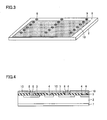
- an N electrode (first layer electrode) 10 electrically connected to N+ layer 4 is formed on passivation film 5, and a P electrode contact 8 electrically connected to P+ layer 3 is formed.
- P electrode contact 8 is formed to project from contact hole 6 provided in passivation film 5.
- N electrode 10 is formed in a region other than regions of contact holes 6, to prevent an electrical short with P electrode contact 8. Although only N electrode 10 may be formed, it is preferable to simultaneously form P electrode contact 8, as will be described later.
- N electrode 10 and P electrode contact 8 are formed by using a paste mainly composed of metal.
- a paste mainly composed of silver or a paste containing a glass frit is used.
- This paste which becomes the electrodes is applied by screen printing.
- a method for applying the paste which becomes the electrodes includes, in addition to screen printing, offset printing, ink-jet printing, and the like.
- the applied paste is then heated.
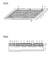
- an insulating layer 11 is formed to cover a surface ofN electrode 10 and expose a surface of P electrode contact 8 by screen printing.
- Insulating layer 11 is formed by applying a paste which is mainly composed of a substance that exhibits electrical insulation properties, and which has a printable viscosity adjusted by a solvent, a thickener, or the like.
- the substance having electrical insulation properties as the main ingredient of the paste examples include an inorganic material such as silica and alumina, or a resin material such as acryl, epoxy, polyimide, a polyimide precursor, and polyamide-imide.
- an elevated temperature of approximately 1000°C is required in order to make a thin and flat insulating layer.
- the resin material on the other hand, the insulating layer is formed like a film due to a heating process of 400°C or less or ultraviolet (UV) irradiation, resulting in difficulty in forming a pin hole. It is therefore preferable that the paste be mainly composed of the resin material.
- the inorganic material may be added to the resin material to provide higher heat resistance. Namely, it is preferable that the insulating paste contain at least one type of the resin materials such as acryl, epoxy, polyimide, a polyimide precursor, and polyamide-imide.
- polyimide, a polyimide precursor, polyamide-imide and the like have relatively high heat resistance for a resin material, and are thus effective when a process at 200°C or more is required.
- Acryl and epoxy have lower heat resistance than that of the polyimide-based materials but come in a variety of types such as a thermosetting type and a UV setting type, and are thus effective when a process at 200°C or more is not required after the insulating layer has been formed.
- a polyimide-based paste include HL-P series manufactured by Hitachi Chemical Company, Ltd.
- examples of an acryl-, epoxy-based paste include UVR-150 series manufactured by Taiyo Ink Mfg. Co., Ltd.
- a polyimide-based paste was used because the paste would be heated at a temperature of approximately 400°C or more during formation of a P electrode which will be described later.
- a solvent ingredient contained in printed insulating layer 11 is vaporized by heating insulating layer 11 at a temperature of 200°C or more, so that insulating layer 11 is formed like a flat film.
- the polyimide precursor is imidized as a result of this heating.
- a method for applying the paste which becomes the insulating layer includes, in addition to screen printing, offset printing, ink-jet printing, and the like.
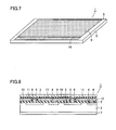
- a P electrode 9 electrically connected to P electrode contact 8 is formed on insulating layer 11 by screen printing.
- P electrode 9 is formed by using a paste mainly composed of metal.
- the applied paste is then fired by performing a prescribed heating process, to complete a solar cell including P electrode 9 and N electrode 10.
- a method for forming the electrodes includes, in addition to screen printing, offset printing, ink-jet printing, and the like.
- the heating process on P electrode 9 is performed with insulating layer 11 being interposed between N electrode 10 and P electrode 9.
- heat resistance of insulating layer 11 was examined.
- Temperatures at which polyimide and a simple polyamide-imide start to be thermally decomposed are generally approximately from 400 to 500°C, although slightly varying with product, with a temperature of thermal decomposition of polyimide being slightly higher.
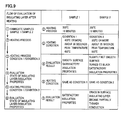
- Fig. 9 illustrates a flow of evaluation and its contents.
- a sample 1 was first subjected to the heating process for about 15 minutes at a temperature of 200°C, and then to a heating process under a heating condition 1 (peak temperature 450°C, about 30 seconds at a temperature of 400°C or more). Observation of the insulating layer after this heating process showed that its surface was smooth and brown peculiar to polyimide.
- a sample 2 was first subjected to the heating process for about 15 minutes at a temperature of 200°C, and then to a heating process under a heating condition 2 (peak temperature 600°C, about 35 seconds at a temperature of 500°C or more). Observation of the insulating layer after this heating process showed that its surface was slightly not smooth and had turned black. It was confirmed that at this point in time, the insulation properties of both sample 1 and sample 2 were satisfactory even after application of a voltage of 10V/ ⁇ m. It is therefore considered that black discoloration in sample 2 was due to occurrence of thermal decomposition only on the surface of the insulating layer.
- sample 1 was subjected to a heating process under the same condition as condition 1, and sample 2 was subjected to a heating process under the same condition as condition 2.
- sample 2 observation of the surface of the insulating layer after the heating processes found that a crack had occurred in the insulating layer, and that the insulating layer had partially become thinner to expose the base silicon substrate. It was confirmed that the insulation properties were lost and conduction was effected in sample 2. In contrast, the insulation properties of sample 1 were satisfactory even after application of a voltage of 10V/ ⁇ m.
- P electrode contact 8 and P electrode 9 were formed in separate steps, N electrode 10 and P electrode contact 8 were formed under a heating condition similar to condition 2, and P electrode 9 was formed under a heating condition similar to condition 1.
- N electrode 10, P electrode 9, and insulating layer 11 are formed by screen printing, and thus can be formed more simply with reduced manufacturing costs as compared to a case where they are formed through photolithography steps and a vacuum process.
- the manufacturing method above has been described with an example of a back surface junction type solar cell including a P+ layer and an N+ layer on the side of a back surface of the solar cell.
- the manufacturing method above is applicable to a solar cell including a P+ electrode and an N+ electrode on one surface of the solar cell.
- the method for forming the electrodes and the method for forming the insulating layer have been described with an example of screen printing.
- Screen printing uses a paste of high viscosity, and allows printing with a line width of approximately 100 ⁇ m, with a printing height of approximately several tens of ⁇ m with respect to a line width of approximately 100 ⁇ m.
- a screen printing apparatus is also relatively simple and has a high processing speed.
- Offset printing uses a paste of low viscosity, and allows printing with a line width of approximately several tens of ⁇ m, with a printing height of approximately several ⁇ m.
- Ink-jet printing uses a paste of low viscosity, and allows printing with a line width of approximately ten to several tens of ⁇ m, with a printing height of approximately several ⁇ m.
- offset printing and ink-jet printing allow high definition printing as compared to screen printing, but are not suitable for thick application.
- Screen printing is capable of thick application, although with a slightly larger line width (approximately 100 ⁇ m), and is thus often used for mass production.
- N electrode 10 and P electrode 9 are formed on substantially the entire surface of solar cell 1, which leads to a larger cross-sectional area of the electrodes than in the past. Accordingly, the electrodes need not be as thick as conventional electrodes, and offset printing and ink-jet printing less suitable for thick printing than screen printing can be applied. Offset printing and ink-jet printing can also be applied to the step of forming contact hole 6 in passivation film 5 and the step of forming insulating layer 11, by adjusting the viscosity of the paste.
- the electrodes may be formed by a plating method, for example, in addition to printing such as screen printing, although the process becomes slightly more complicated than printing.
- a plating method an electrode surface becomes flatter than an electrode surface formed by printing a paste.
- Another advantage is that a temperature of a heating condition for forming an electrode can be lower than a temperature of a heating condition for firing a paste.
- manufactured solar cell 1 has a rectangular shape, with N electrode 10 being exposed along one of four sides, and P electrode 9 being exposed in the remaining region.
- a plurality of solar cells 1 are connected in series by electrically connecting N electrode 10 of one solar cell 1 to P electrode 9 of another solar cell by means of a conducting material including a copper foil, for example, to form a solar cell string 21.
- solar cell string 21 shown in Fig. 10 three solar cells 1 are connected in series in one direction to form one solar cell string, and four solar cell strings are arranged in a direction orthogonal to the one direction.
- P electrode 9 of a solar cell in one solar cell string is electrically connected to N electrode 10 of a solar cell in an adjacent solar cell string by means of a busbar 23.
- thermoplastic translucent sealant Ethylene Vinyl Acetate
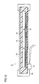
- a translucent substrate 34 such as a glass is provided on the side of the light-receiving surface of solar cell string 21, and a weather-resistant film 33 is provided on the back surface (see Fig. 12 ).
- a heating process is then performed to seal solar cell string 21 in translucent sealant 32, as shown in Fig. 12 .
- a prescribed terminal box 35 is connected and a frame 36 is attached, to complete a solar cell module 31.
- Terminal box 35 incorporates a bypass diode for external connection and for prevention of application of an excessive reverse voltage.
- a method for manufacturing a solar cell and a solar cell module as an example is described.
- a solar cell including P+ layer 3 and N+ layer 4 formed in a back surface of a silicon substrate, passivation film 5 covering the back surface, and antireflection coating 7 formed in a light-receiving surface of the silicon substrate was prepared.
- Silicon substrate 2 was formed in a quasi-square shape (substantially rectangular shape) with one side length of 125 mm.
- P+ layer 3 and N+ layer 4 were alternately formed in lines in the back surface of silicon substrate 2, and a silicon oxide film was formed by thermal oxidation as passivation film 5.
- a silicon nitride film was formed by plasma CVD as antireflection coating 7.
- contact holes 6 having a diameter of 0.1 mm were formed with a pitch of 0.3 mm in portions of passivation film 5 directly above P+ layer 3 and N+ layer 4. Contact holes 6 were formed by screen printing and heating a paste mainly composed of phosphoric acid (see Figs. 1 and 2 ).
- N electrode 10 and P electrode contact 8 were formed.
- P electrode contact 8 was formed in contact hole 6 and N electrode 10 was formed in a shape with a space of about 0.1 mm from P electrode contact 8, each by printing a silver paste into a pattern by screen printing and firing the paste.
- the silver paste used was mainly composed of silver, and contained several percent of glass frit, and an organic solvent and a thickener for adjusting a viscosity.
- the glass frit functions to obtain a favorable degree of contact with silicon substrate 2.
- a heating condition for firing the silver paste was set to a period of 35 seconds at 500°C or more, with a peak temperature of 600°C. As a result of this firing, an organic ingredient in the silver paste was completely decomposed (see Figs. 3 and 4 ).
- a paste mainly composed of a polyimide precursor was applied to a surface ofN electrode 10 to expose only a portion ofN electrode 10 and P electrode contact 8 by screen printing.
- the paste was then heated for about 15 minutes at a temperature of 250°C, to form insulating layer 11 (see Figs. 5 and 6 ).
- a paste mainly composed of silver was printed by screen printing while being prevented from contacting the exposed portion ofN electrode 10, and the paste was fired to form P electrode 8 (see Figs. 7 and 8 ).
- a firing condition was set to a period of 30 seconds at 400°C or more, with a peak temperature of 450°C, so as not to break insulating layer 11.
- the silver paste used did not contain a glass frit and contained only an organic ingredient except silver, in contrast to the silver paste used for forming N electrode 10 and P electrode contact 8. By using such silver paste, low electrical resistivity can be obtained even after firing at a low temperature (see Figs. 8 and 9 ).
- a solar cell module was fabricated by using the solar cells thus manufactured.
- three solar cells 1 were connected in series by means of conducting material 22 including a copper foil covered with solder.
- Conducting material 22 had a length (120 mm) substantially the same as a width of silicon substrate 2, in order to lower series resistance among solar cells 1.
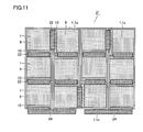
- Three solar cells 1 were connected in series in this manner to form one solar cell string, and four solar cell strings were fabricated. Particularly, in three of the four solar cell strings, the series connection was such that a position ofN electrode 10 of one solar cell 1 located at an end was rotated by 90° with respect to a position ofN electrodes 10 of the other two solar cells 1. As a result, the one solar cell 1 could be connected to solar cell 1 in another solar cell string by means of the same conducting material 22 that was used for connection of solar cells 1 in the solar cell string (see Fig. 11 ).
- N electrode 10 and P electrode 9 are each formed like a layer, and are formed on substantially the entire back surface of silicon substrate 2 with insulating layer 11 interposed between N electrode 10 and P electrode 9. As a result, solar cell 1 having a very high F.F can be manufactured.
- such layered N electrode 10, P electrode 9, and insulating layer 11 can be formed very easily with substantially reduced production costs by screen printing, as compared to a case where they are formed through photolithography and a vacuum process.
- solar cells 1 (or solar cell strings) can be wired without a busbar, thereby improving a F.F. of solar cell module 31 as well.
- the method for manufacturing a solar cell, the method for manufacturing a solar cell module, and the solar cell module according to the present invention are effectively utilized in photoelectric conversion techniques.
Landscapes
- Photovoltaic Devices (AREA)
Abstract
With screen printing, an N electrode (10) electrically connected to an N+ layer (4) is formed on a passivation film (5), and a P electrode contact (8) electrically connected to a P+ layer (3) is formed. Then, with screen printing, an insulating layer (11) is formed to cover a surface of the N electrode (10) and expose a surface of the P electrode contact (8). After that, with screen printing, a P electrode (9) electrically connected to the P electrode contact (8) is formed on the insulating layer (11).
Description
- The present invention relates to a method for manufacturing a solar cell, a method for manufacturing a solar cell module, and a solar cell module, and more particularly to a method for manufacturing a solar cell including layered electrodes, a solar cell module having such solar cells connected in series, and a method for manufacturing thereof.
- In recent years, development of clean energy sources has been desired against the backdrop of the problem of exhaustion of energy resources or global environmental problems due to increase in greenhouse gases typified by CO2 in the atmosphere. Solar power generation using solar batteries (cells, modules), particularly, has been developed and practically utilized as one of such energy sources, making continued progress.
- Conventional solar cells mostly employ a single crystalline or polycrystalline silicon substrate of one conductivity type. In this type of solar cell, an impurity of the opposite conductivity type is diffused into a light-receiving surface of the silicon substrate of one conductivity type to form a p-n junction, and an electrode is formed on each of the light-receiving surface and a back surface of the silicon substrate. Also developed is a solar cell in which a silicon substrate of one conductivity type includes an impurity layer containing a high concentration of impurity of the same conductivity type formed in a back surface of the silicon substrate, thereby achieving high output owing to a back surface electric field effect.
- A so-called back surface junction type solar cell (or a back surface electrode type solar cell) in which an electrode is not formed on a light-receiving surface of a silicon substrate and a p-n junction is formed in a back surface of the silicon substrate has also been developed (see Japanese National Patent Publication No.
2006-523025 4,234,352 (Patent Document 2)). Since an electrode is not formed on the light-receiving surface, this kind of back surface junction type solar cell does not have shadow loss caused by the electrode, and is expected to obtain higher output than a solar cell including an electrode on each of a light-receiving surface and a back surface of a silicon substrate. - Patent Document 1: Japanese National Patent Publication No.
2006-523025 - Patent Document 2: United States Patent No.
4,234,352 - The conventional solar cells (modules) suffer from the following problems, however. First, the back surface electrode type solar cell includes all of a P+ layer, an N+ layer, a P type electrode, and an N type electrode in/on a back surface of the solar cell, resulting in a complicated structure of the solar cell. Additionally, since this type of solar cells are connected in series to manufacture a solar cell module, busbar electrodes for the P type electrode and the N type electrode must be provided on opposing ends of the solar cell.
- For this reason, a finger electrode needs to have a length substantially the same as a width of a silicon substrate of the solar cell, resulting in an increased value of a flowing current per finger electrode. As shown in
Fig. 13 , aP type electrode 108 and anN type electrode 109 exposed at a surface of asilicon substrate 102 covered with apassivation film 105 are formed like teeth of a comb, and provided facing each other with their teeth being interdigitated with one another. - For this reason, a line width of a finger electrode needs to be designed such that the P type electrode and the N type electrode do not contact each other. Without a sufficient line width, however, a F.F (Fill Factor) decreases due to a series resistance component, resulting in reduced output of the solar cell. The F.F. is a parameter that represents inclination of a current-voltage characteristic curve as a solar cell, and is defined as a value obtained by dividing maximum power by the product of an open-circuit voltage and a short circuit current.
-
Patent Document 2 proposes a structure including two layers of a P type electrode and an N type electrode, with a silicon oxide film interposed between the two layers as an insulating layer. This structure is described as having an effect of back surface reflection of a solar cell. By forming the P type electrode and the N type electrode on substantially the entire back surface of the solar cell based on this structure, electrical resistance of the P(N) type electrode(s) can be reduced, thereby obtaining a high F.F. - Unfortunately, in this solar cell, the P type electrode, the N type electrode, and the insulating layer are formed through photolithography steps and a vacuum process such as a vacuum evaporation method. This requires complicated steps and increases manufacturing costs, which renders this solar cell unsuitable for mass production. Additionally, if a busbar is used when connecting the solar cells in series to manufacture a solar cell module, a F.F decreases.
- The present invention was made to solve the problems described above, and an object of the present invention is to provide a method for manufacturing a solar cell applicable to mass production by a simpler process and the solar cell, another object is to provide a method for manufacturing a solar cell module which ensures a F.F. by using such solar cells, and still another object is to provide such solar cell module.
- A method for manufacturing a solar cell according to the present invention includes the following steps. A first electrode is formed on a main surface of a silicon substrate by supplying a conducting material. An insulating layer is formed on a surface of the first electrode by applying an insulating material. A second electrode is formed on a surface of the insulating layer in a manner electrically isolated from the first electrode by supplying a conducting material.
- With this method, the first electrode and the second electrode are formed by supplying the conducting material, and the insulating layer is formed by applying the insulating material. Therefore, the electrodes and the insulating layer are formed in a much simpler manner as compared to a case where photolithography and a vacuum process are used. This facilitates application to mass production, and reduces production costs.
- Specifically, in the step of forming the insulating layer, one of a screen printing method, an offset printing method, and an ink-jet printing method is preferably applied.
- In order to ensure insulation properties of the insulating layer, the step of forming the insulating layer preferably includes, after the application of the insulating material, the step of heating the applied insulating material or the step of curing the applied insulating material by ultraviolet irradiation.
- A heating temperature in the heating step is preferably set to 150°C or more and 600°C or less.
- This is because if the heating temperature is less than 150°C, a solvent contained in the applied insulating material cannot be removed, and if the heating temperature is more than 600°C, a crack occurs in the insulating layer and the insulation properties cannot be ensured.
- Specifically, the insulating material preferably includes at least one of acryl, epoxy, polyimide, a polyimide precursor, and polyamide-imide.
- In at least one of the step of forming the first electrode and the step of forming the second electrode, one of a screen printing method, an offset printing method, and an ink-jet printing method is preferably applied.
- At least one of the step of forming the first electrode and the step of forming the second electrode preferably includes the step of applying a silver paste as the insulating material, and heating the applied silver paste.
- It is preferable that the step of forming the first electrode include a first heating step of heating the supplied conducting material, that the step of forming the second electrode include a second heating step of heating the supplied conducting material and the first electrode heated in the first heating step, and that a temperature in the second heating step be set to 150°C or more and 600°C or less.
- A method for manufacturing another solar cell according to the present invention includes the following steps. A first electrode is formed on a main surface of a silicon substrate by applying and heating a conducting material, the first electrode being electrically connected to a prescribed region in the silicon substrate,. An insulating layer is formed on a surface of the first electrode by applying and heating an insulating material. A second electrode is formed on a surface of the insulating layer by applying and heating a conducting material, the second electrode being electrically isolated from the first electrode and electrically connected to another prescribed region in the silicon substrate,.
- With this method, the first electrode and the second electrode are formed by applying and heating the conducting material, and the insulating layer is formed by applying the insulating material. Therefore, the first electrode, the second electrode, and the insulating layer are formed in a much simpler manner as compared to a case where photolithography and a vacuum process are used. This facilitates application to mass production, and reduces production costs.
- In at least one of the step of forming the first electrode, the step of forming the second electrode, and the step of forming the insulating layer, one of a screen printing method, an offset printing method, and an ink-jet printing method is preferably applied.
- In the step of forming the first electrode, a second electrode contact portion electrically connected to the another prescribed region may be simultaneously formed, and in the step of forming the second electrode, the second electrode may be formed to be electrically connected to the second electrode contact portion.
- In order to lower a heating temperature during formation of the second electrode, it is preferable that in the step of forming the second electrode, a silver paste be applied as the conducting material, and that the silver paste contain only an organic ingredient except silver.
- A solar cell according to the present invention includes a first electrode, an insulating layer, and a second electrode. The first electrode is formed on a main surface of a rectangular silicon substrate. The insulating layer is formed on a surface of the first electrode to expose a surface of a portion of a region of the first electrode along a prescribed first side of the rectangular silicon substrate. The second electrode is formed on a surface of the insulating layer in a manner electrically isolated from the first electrode. The insulating layer includes at least one material selected from the group consisting of acryl, epoxy, polyimide, a polyimide precursor, and polyamide-imide.
- According to this solar cell, a plurality of the solar cells can be connected in series by electrically connecting the portion of the region of the first electrode of one solar cell to the portion of the second electrode of another solar cell.
- In a method for manufacturing a solar cell module having the solar cells manufactured by the method for manufacturing a solar cell according to any of
claims 1 to 12 connected in series according to the present invention, a rectangular silicon substrate is used as the silicon substrate, and in the step of forming the insulating layer in each of the plurality of solar cells, the insulating layer is formed on a surface of the first electrode to expose a surface of a portion of a region of the first electrode along a prescribed first side of the rectangular silicon substrate, the method includes a string formation step of forming a first solar cell string and a second solar cell string by connecting a prescribed number of the solar cells in series, respectively, and a string connection step of connecting the first solar cell string to the second solar cell string in series. In the string formation step, a first solar cell located at an end in the first solar cell string and a second solar cell located at an end in the second solar cell string are arranged such that the first side of the first solar cell faces a third side or a fourth side other than a second side facing the first side of the second solar cell. In the string connection step, a portion of a region of the first electrode positioned along the first side of the first solar cell is electrically connected to a portion of the second electrode positioned along the third side or the fourth side of the second solar cell by means of a prescribed conducting member. - According to this structure, in the first solar cell string and the second solar cell string, the portion of the region of the first electrode positioned along the first side of the first solar cell is electrically connected to the portion of the second electrode positioned along the third side or the fourth side of the second solar cell by means of the prescribed conducting member. Therefore, a conducting member the same as the conducting member for electrically connecting the solar cells in the first solar cell string or the second solar cell string can be used as that conducting member. As a result, reduction in F.F caused by use of a busbar can be prevented.
- Another solar cell module according to the present invention is a solar cell module including a plurality of solar cell strings each having a plurality of solar cells connected in series. Each of the plurality of solar cells includes a first electrode, an insulating layer, and a second electrode. The first electrode is formed on a main surface of a rectangular silicon substrate. The insulating layer is formed on a surface of the first electrode to expose a surface of a portion of a region of the first electrode along a prescribed first side of the rectangular silicon substrate. The second electrode is formed on a surface of the insulating layer in a manner electrically isolated from the first electrode. In a first solar cell string and a second solar cell string adjacent to each other of the plurality of solar cell strings, a first solar cell located at an end in the first solar cell string and a second solar cell located at an end in the second solar cell string are arranged such that the first side of the first solar cell faces a third side or a fourth side other than a second side facing the first side of the second solar cell. A portion of a region of the first electrode positioned along the first side of the first solar cell is electrically connected to a portion of the second electrode positioned along the third side or the fourth side of the second solar cell by means of a prescribed conducting member.
- According to this structure, the portion of the region of the first electrode positioned along the first side of the first solar cell is electrically connected to the portion of the second electrode positioned along the third side or the fourth side of the second solar cell by means of a prescribed conducting member. Therefore, a conducting member the same as the conducting member for electrically connecting the solar cells in the first solar cell string or the second solar cell string can be used as that conducting member. As a result, reduction in F.F caused by use of a busbar can be prevented.
-
-
Fig. 1 is a perspective view showing a step of a method for manufacturing a solar cell according to a first embodiment of the present invention. -
Fig. 2 is a partial cross-sectional view in the step shown inFig. 1 according to the same embodiment. -
Fig. 3 is a perspective view showing a step performed after the step shown inFig. 1 according to the same embodiment. -
Fig. 4 is a partial cross-sectional view in the step shown inFig. 3 according to the same embodiment. -
Fig. 5 is a perspective view showing a step performed after the step shown inFig. 3 according to the same embodiment. -
Fig. 6 is a partial cross-sectional view in the step shown inFig. 5 according to the same embodiment. -
Fig. 7 is a perspective view showing a step performed after the step shown inFig. 5 according to the same embodiment. -
Fig. 8 is a partial cross-sectional view in the step shown inFig. 7 according to the same embodiment. -
Fig. 9 illustrates evaluation of insulating layers after being heated according to the same embodiment. -
Fig. 10 is a plan view showing an example of connection among solar cells in a solar cell module according to a second embodiment of the present invention. -
Fig. 11 is a plan view showing a preferable example of connection among the solar cells in the solar cell module according to the same embodiment. -
Fig. 12 is a cross-sectional view showing the solar cell module according to the same embodiment. -
Fig. 13 is a perspective view showing an example of a conventional solar cell. - 1 solar cell; 2 silicon substrate; 3 P+ layer; 4 N+ layer; 5 passivation film; 6 contact hole; 7 antireflection coating; 8 P electrode contact; 9 P electrode; 10 N electrode; 11 insulating layer; 21 solar cell string; 22 conducting member; 23 busbar; 24 external terminal; 31 solar cell module; 32 translucent sealant; 33 weather-resistant film; 34 translucent substrate; 35 terminal box; 36 frame.
- A method for manufacturing a solar cell is described. First, as shown in
Figs. 1 and 2 , aP+ layer 3 and anN+ layer 4 are alternately formed in lines, for example, in a back surface (face opposite to a light-receiving surface) of asilicon substrate 2. Then, apassivation film 5 is formed to cover the back surface. Contact holes 6 through which surfaces ofP+ layer 3 andN+ layer 4 are exposed are formed inpassivation film 5. Contact holes 6 can be formed in dots or in lines by printing and heating a paste with whichpassivation film 5 can be etched into a desired shape. Anantireflection coating 7 is formed in the light-receiving surface ofsilicon substrate 2. - Next, as shown in
Figs. 3 and 4 , an N electrode (first layer electrode) 10 electrically connected toN+ layer 4 is formed onpassivation film 5, and aP electrode contact 8 electrically connected toP+ layer 3 is formed.P electrode contact 8 is formed to project fromcontact hole 6 provided inpassivation film 5.N electrode 10 is formed in a region other than regions ofcontact holes 6, to prevent an electrical short withP electrode contact 8. Although onlyN electrode 10 may be formed, it is preferable to simultaneously formP electrode contact 8, as will be described later. -
N electrode 10 andP electrode contact 8 are formed by using a paste mainly composed of metal. In order to obtain a high degree of contact withsilicon substrate 2 and keep resistivity of the electrodes themselves low, it is preferable to use a paste mainly composed of silver or a paste containing a glass frit. This paste which becomes the electrodes is applied by screen printing. A method for applying the paste which becomes the electrodes includes, in addition to screen printing, offset printing, ink-jet printing, and the like. - The applied paste is then heated. Here, it is important to heat the paste to a sufficient degree. This is because if an organic ingredient contained in the paste which becomes the electrodes is not vaporized to a sufficient degree, an insulating layer to be subsequently formed will have bulges and holes, which may cause conduction between two electrodes positioned with the insulating layer interposed therebetween. For this reason, it is preferable to perform the heating process at a temperature of at least 150°C or more, and more preferable to fire the paste at an elevated temperature of 400°C or more, to obtain contact between the paste which becomes the electrodes and
silicon substrate 2. - Next, as shown in
Figs. 5 and 6 , an insulatinglayer 11 is formed to cover asurface ofN electrode 10 and expose a surface ofP electrode contact 8 by screen printing. Insulatinglayer 11 is formed by applying a paste which is mainly composed of a substance that exhibits electrical insulation properties, and which has a printable viscosity adjusted by a solvent, a thickener, or the like. - Examples of the substance having electrical insulation properties as the main ingredient of the paste include an inorganic material such as silica and alumina, or a resin material such as acryl, epoxy, polyimide, a polyimide precursor, and polyamide-imide. With only the inorganic material, an elevated temperature of approximately 1000°C is required in order to make a thin and flat insulating layer. With the resin material, on the other hand, the insulating layer is formed like a film due to a heating process of 400°C or less or ultraviolet (UV) irradiation, resulting in difficulty in forming a pin hole. It is therefore preferable that the paste be mainly composed of the resin material. The inorganic material may be added to the resin material to provide higher heat resistance. Namely, it is preferable that the insulating paste contain at least one type of the resin materials such as acryl, epoxy, polyimide, a polyimide precursor, and polyamide-imide.
- Of the resin materials, polyimide, a polyimide precursor, polyamide-imide and the like have relatively high heat resistance for a resin material, and are thus effective when a process at 200°C or more is required. Acryl and epoxy have lower heat resistance than that of the polyimide-based materials but come in a variety of types such as a thermosetting type and a UV setting type, and are thus effective when a process at 200°C or more is not required after the insulating layer has been formed. Examples of a polyimide-based paste include HL-P series manufactured by Hitachi Chemical Company, Ltd., and examples of an acryl-, epoxy-based paste include UVR-150 series manufactured by Taiyo Ink Mfg. Co., Ltd.
- Here, a polyimide-based paste was used because the paste would be heated at a temperature of approximately 400°C or more during formation of a P electrode which will be described later. When a polyimide-based paste is used, a solvent ingredient contained in printed insulating
layer 11 is vaporized by heating insulatinglayer 11 at a temperature of 200°C or more, so that insulatinglayer 11 is formed like a flat film. When a polyimide precursor is used as the paste, the polyimide precursor is imidized as a result of this heating. A method for applying the paste which becomes the insulating layer includes, in addition to screen printing, offset printing, ink-jet printing, and the like. - Next, as shown in
Figs. 7 and 8 , aP electrode 9 electrically connected toP electrode contact 8 is formed on insulatinglayer 11 by screen printing. As withN electrode 10,P electrode 9 is formed by using a paste mainly composed of metal. The applied paste is then fired by performing a prescribed heating process, to complete a solar cell includingP electrode 9 andN electrode 10. A method for forming the electrodes includes, in addition to screen printing, offset printing, ink-jet printing, and the like. - The heating process on
P electrode 9 is performed with insulatinglayer 11 being interposed betweenN electrode 10 andP electrode 9. Thus, heat resistance of insulatinglayer 11 was examined. Temperatures at which polyimide and a simple polyamide-imide start to be thermally decomposed are generally approximately from 400 to 500°C, although slightly varying with product, with a temperature of thermal decomposition of polyimide being slightly higher. - Accordingly, an insulating paste of the HL-P500 manufactured by Hitachi Chemical Company, Ltd. described above, which alters to polyimide when heated, was directly printed on a silicon substrate, heated for about 15 minutes at a temperature of 200°C, further heated thereafter under an electrode firing condition, and insulation properties after the heating were evaluated.
Fig. 9 illustrates a flow of evaluation and its contents. - A
sample 1 was first subjected to the heating process for about 15 minutes at a temperature of 200°C, and then to a heating process under a heating condition 1 (peak temperature 450°C, about 30 seconds at a temperature of 400°C or more). Observation of the insulating layer after this heating process showed that its surface was smooth and brown peculiar to polyimide. - A
sample 2 was first subjected to the heating process for about 15 minutes at a temperature of 200°C, and then to a heating process under a heating condition 2 (peak temperature 600°C, about 35 seconds at a temperature of 500°C or more). Observation of the insulating layer after this heating process showed that its surface was slightly not smooth and had turned black. It was confirmed that at this point in time, the insulation properties of bothsample 1 andsample 2 were satisfactory even after application of a voltage of 10V/µm. It is therefore considered that black discoloration insample 2 was due to occurrence of thermal decomposition only on the surface of the insulating layer. - Subsequently,
sample 1 was subjected to a heating process under the same condition ascondition 1, andsample 2 was subjected to a heating process under the same condition ascondition 2. Insample 2, observation of the surface of the insulating layer after the heating processes found that a crack had occurred in the insulating layer, and that the insulating layer had partially become thinner to expose the base silicon substrate. It was confirmed that the insulation properties were lost and conduction was effected insample 2. In contrast, the insulation properties ofsample 1 were satisfactory even after application of a voltage of 10V/µm. - These evaluation results showed that a heating condition for insulating
layer 11 had an upper limit of a period of 35 seconds at a temperature of 500°C or more. Then, based on these evaluation results,P electrode 9 was formed by using a silver paste that can be fired under a heating condition similar tocondition 1. Since this silver paste contains only a resin ingredient other than silver powders, a value of electrical resistivity would be sufficiently low even after heating at a temperature lower than that ofcondition 1. However, such heating results in higher contact resistance with the silicon substrate. Additionally, since this silver paste provides low electrical resistance even after heated at 200°C or less, an acryl- or epoxy-based insulating paste can also be used. However, heating at 200°C or less takes a very long time for heating. Thus, the paste was fired under a heating condition similar tocondition 1. - Therefore, during actual manufacture,
P electrode contact 8 andP electrode 9 were formed in separate steps,N electrode 10 andP electrode contact 8 were formed under a heating condition similar tocondition 2, andP electrode 9 was formed under a heating condition similar tocondition 1. - It should be noted that, because the insulation properties were satisfactory after heating under
condition 2 only once, a method of using a paste capable of obtaining favorable contact with silicon to print anddry N electrode 10, then print and dry the insulating layer, then print anddry P electrode 9 with the paste, and then fire them together undercondition 2 can be employed, thereby further simplifying the process. - With the manufacturing method above,
N electrode 10,P electrode 9, and insulatinglayer 11 are formed by screen printing, and thus can be formed more simply with reduced manufacturing costs as compared to a case where they are formed through photolithography steps and a vacuum process. - The manufacturing method above has been described with an example of a back surface junction type solar cell including a P+ layer and an N+ layer on the side of a back surface of the solar cell. The manufacturing method above is applicable to a solar cell including a P+ electrode and an N+ electrode on one surface of the solar cell.
- The method for forming the electrodes and the method for forming the insulating layer have been described with an example of screen printing. Screen printing uses a paste of high viscosity, and allows printing with a line width of approximately 100 µm, with a printing height of approximately several tens of µm with respect to a line width of approximately 100 µm. A screen printing apparatus is also relatively simple and has a high processing speed.
- In addition to screen printing, offset printing and ink-jet printing may be applied, as described above. Offset printing uses a paste of low viscosity, and allows printing with a line width of approximately several tens of µm, with a printing height of approximately several µm. Ink-jet printing uses a paste of low viscosity, and allows printing with a line width of approximately ten to several tens of µm, with a printing height of approximately several µm.
- As such, offset printing and ink-jet printing allow high definition printing as compared to screen printing, but are not suitable for thick application. Screen printing is capable of thick application, although with a slightly larger line width (approximately 100 µm), and is thus often used for mass production.
- In the solar cell described above,
N electrode 10 andP electrode 9 are formed on substantially the entire surface ofsolar cell 1, which leads to a larger cross-sectional area of the electrodes than in the past. Accordingly, the electrodes need not be as thick as conventional electrodes, and offset printing and ink-jet printing less suitable for thick printing than screen printing can be applied. Offset printing and ink-jet printing can also be applied to the step of formingcontact hole 6 inpassivation film 5 and the step of forming insulatinglayer 11, by adjusting the viscosity of the paste. - The electrodes may be formed by a plating method, for example, in addition to printing such as screen printing, although the process becomes slightly more complicated than printing. With a plating method, an electrode surface becomes flatter than an electrode surface formed by printing a paste. Another advantage is that a temperature of a heating condition for forming an electrode can be lower than a temperature of a heating condition for firing a paste.
- A method for manufacturing a solar cell module by using the solar cells fabricated in the previous embodiment is described. As shown in
Fig. 7 , manufacturedsolar cell 1 has a rectangular shape, withN electrode 10 being exposed along one of four sides, andP electrode 9 being exposed in the remaining region. As shown inFig. 10 , a plurality ofsolar cells 1 are connected in series by electrically connectingN electrode 10 of onesolar cell 1 toP electrode 9 of another solar cell by means of a conducting material including a copper foil, for example, to form asolar cell string 21. - In
solar cell string 21 shown inFig. 10 , threesolar cells 1 are connected in series in one direction to form one solar cell string, and four solar cell strings are arranged in a direction orthogonal to the one direction.P electrode 9 of a solar cell in one solar cell string is electrically connected toN electrode 10 of a solar cell in an adjacent solar cell string by means of abusbar 23. - Of
solar cells 1 in the solar cell strings shown inFig. 10 (comparative example), it is preferable to rotate solar cells 1a, 1b, and 1c by 90° so thatN electrode 10 is positioned alongP electrode 9 of adjacentsolar cell 1. As a result,P electrode 9 of a solar cell in one solar cell string can be electrically connected toN electrode 10 of a solar cell in an adjacent solar cell string by means of a conducting material 22, thus eliminating the need to attach a busbar. - When a busbar is applied, it is difficult to ensure a sufficient width of the busbar in terms of design of a solar cell module. Thus, resistance loss in the busbar may result in reduction in F.F. By not applying a busbar, therefore, reduction in F.F after a solar cell module has been formed can be minimized, thereby obtaining high output. In addition, since this
solar cell 1 does not include an electrode on the side of the light-receiving surface, change in orientation ofsolar cells 1 poses no problem in terms of appearance. - Next,
solar cell string 21 thus formed is inserted into a thermoplastic translucent sealant (EVA: Ethylene Vinyl Acetate) 32. Then, atranslucent substrate 34 such as a glass is provided on the side of the light-receiving surface ofsolar cell string 21, and a weather-resistant film 33 is provided on the back surface (seeFig. 12 ). A heating process is then performed to sealsolar cell string 21 intranslucent sealant 32, as shown inFig. 12 . After that, aprescribed terminal box 35 is connected and aframe 36 is attached, to complete asolar cell module 31.Terminal box 35 incorporates a bypass diode for external connection and for prevention of application of an excessive reverse voltage. - A method for manufacturing a solar cell and a solar cell module as an example is described.
- First, as a solar cell, a solar cell including
P+ layer 3 andN+ layer 4 formed in a back surface of a silicon substrate,passivation film 5 covering the back surface, andantireflection coating 7 formed in a light-receiving surface of the silicon substrate was prepared.Silicon substrate 2 was formed in a quasi-square shape (substantially rectangular shape) with one side length of 125 mm.P+ layer 3 andN+ layer 4 were alternately formed in lines in the back surface ofsilicon substrate 2, and a silicon oxide film was formed by thermal oxidation aspassivation film 5. A silicon nitride film was formed by plasma CVD asantireflection coating 7. - Next, contact holes 6 having a diameter of 0.1 mm were formed with a pitch of 0.3 mm in portions of
passivation film 5 directly aboveP+ layer 3 andN+ layer 4. Contact holes 6 were formed by screen printing and heating a paste mainly composed of phosphoric acid (seeFigs. 1 and 2 ). - Next,
N electrode 10 andP electrode contact 8 were formed.P electrode contact 8 was formed incontact hole 6 andN electrode 10 was formed in a shape with a space of about 0.1 mm fromP electrode contact 8, each by printing a silver paste into a pattern by screen printing and firing the paste. The silver paste used was mainly composed of silver, and contained several percent of glass frit, and an organic solvent and a thickener for adjusting a viscosity. The glass frit functions to obtain a favorable degree of contact withsilicon substrate 2. A heating condition for firing the silver paste was set to a period of 35 seconds at 500°C or more, with a peak temperature of 600°C. As a result of this firing, an organic ingredient in the silver paste was completely decomposed (seeFigs. 3 and 4 ). - Next, a paste mainly composed of a polyimide precursor was applied to a
surface ofN electrode 10 to expose only aportion ofN electrode 10 andP electrode contact 8 by screen printing. The paste was then heated for about 15 minutes at a temperature of 250°C, to form insulating layer 11 (seeFigs. 5 and 6 ). - Next, a paste mainly composed of silver was printed by screen printing while being prevented from contacting the exposed
portion ofN electrode 10, and the paste was fired to form P electrode 8 (seeFigs. 7 and 8 ). A firing condition was set to a period of 30 seconds at 400°C or more, with a peak temperature of 450°C, so as not to break insulatinglayer 11. In addition, since the paste was to be fired at a temperature lower than that during firing in the step shown inFig. 4 , the silver paste used did not contain a glass frit and contained only an organic ingredient except silver, in contrast to the silver paste used for formingN electrode 10 andP electrode contact 8. By using such silver paste, low electrical resistivity can be obtained even after firing at a low temperature (seeFigs. 8 and9 ). - Next, a solar cell module was fabricated by using the solar cells thus manufactured. First, three
solar cells 1 were connected in series by means of conducting material 22 including a copper foil covered with solder. Conducting material 22 had a length (120 mm) substantially the same as a width ofsilicon substrate 2, in order to lower series resistance amongsolar cells 1. - Three
solar cells 1 were connected in series in this manner to form one solar cell string, and four solar cell strings were fabricated. Particularly, in three of the four solar cell strings, the series connection was such that aposition ofN electrode 10 of onesolar cell 1 located at an end was rotated by 90° with respect to aposition ofN electrodes 10 of the other twosolar cells 1. As a result, the onesolar cell 1 could be connected tosolar cell 1 in another solar cell string by means of the same conducting material 22 that was used for connection ofsolar cells 1 in the solar cell string (seeFig. 11 ). - Consequently, reduction in F.F. caused by use of a busbar could be prevented, as compared to the solar cell
strings employing busbar 23 for connection between the solar cell strings (seeFig. 10 ). In this manner,solar cell string 21 having twelvesolar cells 1 connected in series was fabricated (seeFig. 11 ). - Next,
external terminals 24 for external connection were connected to opposing ends ofsolar cell string 21 having four solar cell strings connected in series.Solar cell string 21 was then inserted into translucent sealant (EVA film) 32. Next, translucent substrate (glass plate) 34 was provided on the side of the light-receiving surface and weather-resistant film 33 was provided on the side of the back surface, and they were heated to seal solar cell string 21 (seeFig. 12 ). Then,terminal box 3 5 for external connection was connected andframe 36 was attached, to complete the solar cell module (seeFig. 12 ). - With the method described above,
N electrode 10 andP electrode 9 are each formed like a layer, and are formed on substantially the entire back surface ofsilicon substrate 2 with insulatinglayer 11 interposed betweenN electrode 10 andP electrode 9. As a result,solar cell 1 having a very high F.F can be manufactured. - Moreover, such
layered N electrode 10,P electrode 9, and insulatinglayer 11 can be formed very easily with substantially reduced production costs by screen printing, as compared to a case where they are formed through photolithography and a vacuum process. - Furthermore, in
solar cell module 31 manufactured by using thus fabricatedsolar cells 1, solar cells 1 (or solar cell strings) can be wired without a busbar, thereby improving a F.F. ofsolar cell module 31 as well. - It should be understood that the embodiments and examples disclosed herein are illustrative and non-restrictive in every respect. The scope of the present invention is defined by the terms of the claims, rather than the description above, and is intended to include any modifications within the scope and meaning equivalent to the terms of the claims.
- The method for manufacturing a solar cell, the method for manufacturing a solar cell module, and the solar cell module according to the present invention are effectively utilized in photoelectric conversion techniques.
Claims (15)
- A method for manufacturing a solar cell, comprising the steps of:forming a first electrode (10) on a main surface of a silicon substrate (2) by supplying a conducting material;forming an insulating layer (11) on a surface of said first electrode (10) by applying an insulating material; andforming a second electrode (9) on a surface of said insulating layer (11) in a manner electrically isolated from said first electrode (10) by supplying a conducting material.
- The method for manufacturing a solar cell according to claim 1, wherein
in said step of forming said insulating layer (11), one of a screen printing method, an offset printing method, and an ink-jet printing method is applied. - The method for manufacturing a solar cell according to claim 1, wherein
said step of forming said insulating layer (11) includes, after the application of said insulating material, the step of heating applied said insulating material or the step of irradiating applied said insulating material with ultraviolet rays. - The method for manufacturing a solar cell according to claim 3, wherein
a heating temperature in said heating step is set to 150°C or more and 600°C or less. - The method for manufacturing a solar cell according to claim 1, wherein
in said step of forming said insulating layer (11), said insulating layer (11) includes at least one of acryl, epoxy, polyimide, a polyimide precursor, and polyamide-imide as said insulating material. - The method for manufacturing a solar cell according to claim 1, wherein
in at least one of said step of forming said first electrode (10) and said step of forming said second electrode (9), one of a screen printing method, an offset printing method, and an ink-jet printing method is applied. - The method for manufacturing a solar cell according to claim 6, wherein
at least one of said step of forming said first electrode (10) and said step of forming said second electrode (9) includes the step of applying a silver paste as said insulating material, and heating applied said silver paste. - The method for manufacturing a solar cell according to claim 1, wherein said step of forming said first electrode (10) includes a first heating step of heating supplied said conducting material,
said step of forming said second electrode (9) includes a second heating step of heating supplied said conducting material and said first electrode (10) heated in said first heating step, and
a temperature in said second heating step is set to 150°C or more and 600°C or less. - A method for manufacturing a solar cell, comprising the steps of:forming a first electrode (10) on a main surface of a silicon substrate (2) by applying and heating a conducting material, said first electrode (10) being electrically connected to a prescribed region in said silicon substrate (2);forming an insulating layer (11) on a surface of said first electrode (10) by applying and heating an insulating material; andforming a second electrode (9) on a surface of said insulating layer (11) by applying and heating a conducting material, said second electrode (9) being electrically isolated from said first electrode (10) and electrically connected to another prescribed region in said silicon substrate (2).
- The method for manufacturing a solar cell according to claim 9, wherein
in at least one of said step of forming said first electrode (10), said step of forming said second electrode (9), and said step of forming said insulating layer (11), one of a screen printing method, an offset printing method, and an ink-jet printing method is applied. - The method for manufacturing a solar cell according to claim 9, wherein
in said step of forming said first electrode (10), a second electrode contact portion electrically connected to said another prescribed region is simultaneously formed, and
in said step of forming said second electrode (9), said second electrode (9) is formed to be electrically connected to said second electrode contact portion (8). - The method for manufacturing a solar cell according to claim 9, wherein
in said step of forming said second electrode (9), a silver paste is applied as said conducting material, and
said silver paste contains only an organic ingredient except silver. - A solar cell (1) comprising:a first electrode (10) formed on a main surface of a rectangular silicon substrate (2);an insulating layer (11) formed on a surface of said first electrode (10) to expose a surface of a portion of a region of said first electrode (10) along a prescribed first side of said rectangular silicon substrate (2); anda second electrode (9) formed on a surface of said insulating layer (11) in a manner electrically isolated from said first electrode (10),said insulating layer (11) including at least one material selected from the group consisting of acryl, epoxy, polyimide, a polyimide precursor, and polyamide-imide.
- A method for manufacturing a solar cell module having the solar cells manufactured by the method for manufacturing a solar cell according to any of claims 1 to 12 connected in series, wherein
a rectangular silicon substrate (2) is used as said silicon substrate (2), and
in said step of forming said insulating layer (11) in each of the plurality of solar cells (1), said insulating layer (11) is formed on a surface of said first electrode (10) to expose a surface of a portion of a region of said first electrode (10) along a prescribed first side of said rectangular silicon substrate (2), said method comprises
a string (21) formation step of forming a first solar cell string (21) and a second solar cell string (21) by connecting a prescribed number of said solar cells (1) in series, respectively, and
a string (21) connection step of connecting said first solar cell string (21) to said second solar cell string (21) in series,
in said string (21) formation step, a first solar cell (1) located at an end in said first solar cell string (21) and a second solar cell (1) located at an end in said second solar cell string (21) are arranged such that said first side of said first solar cell (1) faces a third side or a fourth side other than a second side facing said first side of said second solar cell (1), and
in said string (21) connection step, a portion of a region of said first electrode (10) positioned along said first side of said first solar cell (1) is electrically connected to a portion of said second electrode (9) positioned along said third side or said fourth side of said second solar cell (1) by means of a prescribed conducting member. - A solar cell module comprising a plurality of solar cell strings (21) each having a plurality of solar cells connected in series,
each of the plurality of solar cells (1) including
a first electrode (10) formed on a main surface of a rectangular silicon substrate (2),
an insulating layer (11) formed on a surface of said first electrode (10) to expose a surface of a portion of a region of said first electrode (10) along a prescribed first side of said rectangular silicon substrate (2), and
a second electrode (9) formed on a surface of said insulating layer (11) in a manner electrically isolated from said first electrode (10),
in a first solar cell string (21) and a second solar cell string (21) adjacent to each other of the plurality of solar cell strings (21),
a first solar cell (1) located at an end in said first solar cell string (21) and a second solar cell (1) located at an end in said second solar cell string (21) are arranged such that said first side of said first solar cell (1) faces a third side or a fourth side other than a second side facing said first side of said second solar cell (1), and
a portion of a region of said first electrode (10) positioned along said first side of said first solar cell (1) is electrically connected to a portion of said second electrode (9) positioned along said third side or said fourth side of said second solar cell (1) by means of a prescribed conducting member.
Applications Claiming Priority (2)
| Application Number | Priority Date | Filing Date | Title |
|---|---|---|---|
| JP2008100497A JP2009253096A (en) | 2008-04-08 | 2008-04-08 | Solar battery cell manufacturing method, solar battery module manufacturing method, and solar battery module |
| PCT/JP2009/053523 WO2009125628A1 (en) | 2008-04-08 | 2009-02-26 | Solar battery cell manufacturing method, solar battery module manufacturing method, and solar battery module |
Publications (1)
| Publication Number | Publication Date |
|---|---|
| EP2273558A1 true EP2273558A1 (en) | 2011-01-12 |
Family
ID=41161763
Family Applications (1)
| Application Number | Title | Priority Date | Filing Date |
|---|---|---|---|
| EP09730405A Withdrawn EP2273558A1 (en) | 2008-04-08 | 2009-02-26 | Solar battery cell manufacturing method, solar battery module manufacturing method, and solar battery module |
Country Status (4)
| Country | Link |
|---|---|
| US (1) | US20110030759A1 (en) |
| EP (1) | EP2273558A1 (en) |
| JP (1) | JP2009253096A (en) |
| WO (1) | WO2009125628A1 (en) |
Cited By (3)
| Publication number | Priority date | Publication date | Assignee | Title |
|---|---|---|---|---|
| US9559241B2 (en) | 2010-07-09 | 2017-01-31 | Takanoha Trading Co., Ltd. | Panel, method for producing panel, solar cell module, printing apparatus, and printing method |
| EP3349251A4 (en) * | 2016-11-15 | 2018-11-07 | Shin-Etsu Chemical Co., Ltd | High efficiency solar cell and method for manufacturing high efficiency solar cell |
| EP3343643A4 (en) * | 2016-11-07 | 2019-01-23 | Shin-Etsu Chemical Co., Ltd | METHOD FOR MANUFACTURING HIGHLY EFFICIENT SOLAR CELL |
Families Citing this family (16)
| Publication number | Priority date | Publication date | Assignee | Title |
|---|---|---|---|---|
| JP5242499B2 (en) * | 2009-05-25 | 2013-07-24 | シャープ株式会社 | SOLAR CELL MODULE, ITS MANUFACTURING METHOD, AND ELECTRONIC DEVICE MOUNTED WITH THE SOLAR CELL MODULE |
| FR2952474B1 (en) * | 2009-11-06 | 2012-01-06 | Commissariat Energie Atomique | PHOTOVOLTAIC CELL DRIVER WITH TWO HIGH AND LOW TEMPERATURE SERIGRAPHIC PARTS |
| NL2005180C2 (en) * | 2010-07-30 | 2012-01-31 | Stichting Energie | Solar cell module and method for manufacturing such a module. |
| JP2012069594A (en) * | 2010-09-21 | 2012-04-05 | Pi R & D Co Ltd | Polyimide resin composition for forming insulating film in solar cell and method of forming insulating film in solar cell by using the same |
| JP2012084747A (en) * | 2010-10-13 | 2012-04-26 | National Institute Of Advanced Industrial & Technology | Crystal silicon solar cell manufacturing method |
| US8134217B2 (en) | 2010-12-14 | 2012-03-13 | Sunpower Corporation | Bypass diode for a solar cell |
| US8586403B2 (en) * | 2011-02-15 | 2013-11-19 | Sunpower Corporation | Process and structures for fabrication of solar cells with laser ablation steps to form contact holes |
| WO2013140553A1 (en) | 2012-03-21 | 2013-09-26 | 三洋電機株式会社 | Solar cell module |
| CN103928563B (en) * | 2013-01-10 | 2016-01-13 | 杜邦公司 | For the integrated form backboard assembly of photovoltaic module |
| WO2014140713A1 (en) * | 2013-03-11 | 2014-09-18 | Watts & More Ltd. | An energy/power generation system |
| JP6190218B2 (en) * | 2013-09-05 | 2017-08-30 | シャープ株式会社 | Solar cell module and wiring sheet |
| CN106715987A (en) * | 2014-09-08 | 2017-05-24 | 法克有限公司 | Pressure relief device having conductive ink sensors formed thereon |
| CN104282788B (en) * | 2014-09-28 | 2017-03-22 | 苏州中来光伏新材股份有限公司 | Main-grid-free high-efficiency back contact solar cell module, main-grid-free high-efficiency back contact solar cell assembly and manufacturing technology of main-grid-free high-efficiency back contact solar cell assembly |
| CN109804474A (en) * | 2016-09-23 | 2019-05-24 | 石原化学株式会社 | The manufacturing method of solar battery cell |
| US20190237592A1 (en) * | 2018-01-31 | 2019-08-01 | Solaria Corporation | Photovoltaic system and components |
| CN115000198B (en) * | 2022-07-18 | 2023-05-05 | 浙江晶科能源有限公司 | Solar cell and photovoltaic module |
Family Cites Families (9)
| Publication number | Priority date | Publication date | Assignee | Title |
|---|---|---|---|---|
| US4234352A (en) * | 1978-07-26 | 1980-11-18 | Electric Power Research Institute, Inc. | Thermophotovoltaic converter and cell for use therein |
| US5641362A (en) * | 1995-11-22 | 1997-06-24 | Ebara Solar, Inc. | Structure and fabrication process for an aluminum alloy junction self-aligned back contact silicon solar cell |
| JP3676954B2 (en) * | 1999-11-08 | 2005-07-27 | シャープ株式会社 | Photoelectric conversion element and manufacturing method thereof |
| US6274402B1 (en) * | 1999-12-30 | 2001-08-14 | Sunpower Corporation | Method of fabricating a silicon solar cell |
| JP2003298078A (en) * | 2002-03-29 | 2003-10-17 | Ebara Corp | Photovoltaic element |
| US7388147B2 (en) | 2003-04-10 | 2008-06-17 | Sunpower Corporation | Metal contact structure for solar cell and method of manufacture |
| FR2854497B1 (en) * | 2003-04-29 | 2005-09-02 | Commissariat Energie Atomique | METHOD FOR MAKING A SEMICONDUCTOR DEVICE WITH SELF-ALIGNED METALLISATIONS |
| US20050153114A1 (en) * | 2004-01-14 | 2005-07-14 | Rahul Gupta | Printing of organic electronic devices |
| US7122398B1 (en) * | 2004-03-25 | 2006-10-17 | Nanosolar, Inc. | Manufacturing of optoelectronic devices |
-
2008
- 2008-04-08 JP JP2008100497A patent/JP2009253096A/en active Pending
-
2009
- 2009-02-26 US US12/936,657 patent/US20110030759A1/en not_active Abandoned
- 2009-02-26 WO PCT/JP2009/053523 patent/WO2009125628A1/en not_active Ceased
- 2009-02-26 EP EP09730405A patent/EP2273558A1/en not_active Withdrawn
Non-Patent Citations (1)
| Title |
|---|
| See references of WO2009125628A1 * |
Cited By (6)
| Publication number | Priority date | Publication date | Assignee | Title |
|---|---|---|---|---|
| US9559241B2 (en) | 2010-07-09 | 2017-01-31 | Takanoha Trading Co., Ltd. | Panel, method for producing panel, solar cell module, printing apparatus, and printing method |
| EP3343643A4 (en) * | 2016-11-07 | 2019-01-23 | Shin-Etsu Chemical Co., Ltd | METHOD FOR MANUFACTURING HIGHLY EFFICIENT SOLAR CELL |
| US10236397B2 (en) | 2016-11-07 | 2019-03-19 | Shin-Etsu Chemical Co., Ltd. | Method for producing high-efficiency solar cell |
| EP3349251A4 (en) * | 2016-11-15 | 2018-11-07 | Shin-Etsu Chemical Co., Ltd | High efficiency solar cell and method for manufacturing high efficiency solar cell |
| US10998463B2 (en) | 2016-11-15 | 2021-05-04 | Shin-Etsu Chemical Co., Ltd. | High efficiency solar cell and method for manufacturing high efficiency solar cell |
| US11552202B2 (en) | 2016-11-15 | 2023-01-10 | Shin-Etsu Chemical Co., Ltd. | High efficiency solar cell and method for manufacturing high efficiency solar cell |
Also Published As
| Publication number | Publication date |
|---|---|
| US20110030759A1 (en) | 2011-02-10 |
| JP2009253096A (en) | 2009-10-29 |
| WO2009125628A1 (en) | 2009-10-15 |
Similar Documents
| Publication | Publication Date | Title |
|---|---|---|
| EP2273558A1 (en) | Solar battery cell manufacturing method, solar battery module manufacturing method, and solar battery module | |
| EP2184787A1 (en) | Rear surface bonding type solar cell, rear surface bonding type solar cell having wiring board, solar cell string and soar cell module | |
| CN104272475B (en) | The battery of back contact solar photovoltaic module semiconductor wafer and module processing | |
| KR101178765B1 (en) | Solar battery module and method for manufacturing the same | |
| CN106575679B (en) | Solar cell and manufacturing method thereof | |
| US8609983B2 (en) | Interconnection sheet, solar cell with interconnection sheet, solar cell module, and interconnection sheet roll | |
| EP2249397B1 (en) | Solar cell module | |
| JPWO2008090718A1 (en) | Solar cell, solar cell array and solar cell module | |
| US20130298988A1 (en) | Solar battery and method of manufacturing solar battery | |
| EP2284907A1 (en) | Solar battery, method for manufacturing solar battery, and solar battery module | |
| WO2007119365A1 (en) | Solar cell, solar cell string and solar cell module | |
| JP2008282990A (en) | SOLAR CELL, SOLAR CELL MANUFACTURING METHOD, SOLAR CELL STRING AND SOLAR CELL MODULE | |
| WO2015190024A1 (en) | Solar cell and method for manufacturing solar cell | |
| JP5126878B2 (en) | Solar cell manufacturing method and solar cell | |
| US20140210073A1 (en) | Conductive paste, electrode for semiconductor device, semiconductor device, and method for manufacturing semiconductor device | |
| KR20120069671A (en) | Electrically conductive paste, electrode for semiconductor device, semiconductor device, and process for production of semiconductor device | |
| EP1840916A1 (en) | A sealed monolithic photo-electrochemical system and a method for manufacturing a sealed monolithic photo-electrochemical system | |
| JP4185332B2 (en) | Solar cell and solar cell module using the same | |
| JP4040662B1 (en) | Solar cell, solar cell string and solar cell module | |
| JP4519089B2 (en) | Solar cell, solar cell string and solar cell module | |
| US20130104976A1 (en) | Solar cell with interconnection sheet, solar cell module, and method for manufacturing solar cell with interconnection sheet | |
| JP4931445B2 (en) | Solar cell with interconnector, solar cell string and solar cell module | |
| JP5196418B2 (en) | Solar cell and solar cell module with interconnector | |
| JP2007288113A (en) | Solar cell, solar cell string and solar cell module | |
| JP2007165785A (en) | Solar cell with interconnector, solar cell string and solar cell module |
Legal Events
| Date | Code | Title | Description |
|---|---|---|---|
| PUAI | Public reference made under article 153(3) epc to a published international application that has entered the european phase |
Free format text: ORIGINAL CODE: 0009012 |
|
| 17P | Request for examination filed |
Effective date: 20101015 |
|
| AK | Designated contracting states |
Kind code of ref document: A1 Designated state(s): AT BE BG CH CY CZ DE DK EE ES FI FR GB GR HR HU IE IS IT LI LT LU LV MC MK MT NL NO PL PT RO SE SI SK TR |
|
| AX | Request for extension of the european patent |
Extension state: AL BA RS |
|
| DAX | Request for extension of the european patent (deleted) | ||
| STAA | Information on the status of an ep patent application or granted ep patent |
Free format text: STATUS: THE APPLICATION HAS BEEN WITHDRAWN |
|
| 18W | Application withdrawn |
Effective date: 20130328 |