EP2273356B1 - Multi-touch detecting method for detecting locations of touched points on a touch panel - Google Patents
Multi-touch detecting method for detecting locations of touched points on a touch panel Download PDFInfo
- Publication number
- EP2273356B1 EP2273356B1 EP10168940.4A EP10168940A EP2273356B1 EP 2273356 B1 EP2273356 B1 EP 2273356B1 EP 10168940 A EP10168940 A EP 10168940A EP 2273356 B1 EP2273356 B1 EP 2273356B1
- Authority
- EP
- European Patent Office
- Prior art keywords
- measuring point
- voltage
- location
- conductive film
- measured
- Prior art date
- Legal status (The legal status is an assumption and is not a legal conclusion. Google has not performed a legal analysis and makes no representation as to the accuracy of the status listed.)
- Active
Links
Images



Classifications
-
- G—PHYSICS
- G06—COMPUTING OR CALCULATING; COUNTING
- G06F—ELECTRIC DIGITAL DATA PROCESSING
- G06F3/00—Input arrangements for transferring data to be processed into a form capable of being handled by the computer; Output arrangements for transferring data from processing unit to output unit, e.g. interface arrangements
- G06F3/01—Input arrangements or combined input and output arrangements for interaction between user and computer
- G06F3/03—Arrangements for converting the position or the displacement of a member into a coded form
- G06F3/041—Digitisers, e.g. for touch screens or touch pads, characterised by the transducing means
- G06F3/045—Digitisers, e.g. for touch screens or touch pads, characterised by the transducing means using resistive elements, e.g. a single continuous surface or two parallel surfaces put in contact
-
- G—PHYSICS
- G06—COMPUTING OR CALCULATING; COUNTING
- G06F—ELECTRIC DIGITAL DATA PROCESSING
- G06F3/00—Input arrangements for transferring data to be processed into a form capable of being handled by the computer; Output arrangements for transferring data from processing unit to output unit, e.g. interface arrangements
- G06F3/01—Input arrangements or combined input and output arrangements for interaction between user and computer
- G06F3/03—Arrangements for converting the position or the displacement of a member into a coded form
- G06F3/033—Pointing devices displaced or positioned by the user, e.g. mice, trackballs, pens or joysticks; Accessories therefor
- G06F3/0354—Pointing devices displaced or positioned by the user, e.g. mice, trackballs, pens or joysticks; Accessories therefor with detection of two-dimensional [2D] relative movements between the device, or an operating part thereof, and a plane or surface, e.g. 2D mice, trackballs, pens or pucks
-
- G—PHYSICS
- G06—COMPUTING OR CALCULATING; COUNTING
- G06F—ELECTRIC DIGITAL DATA PROCESSING
- G06F3/00—Input arrangements for transferring data to be processed into a form capable of being handled by the computer; Output arrangements for transferring data from processing unit to output unit, e.g. interface arrangements
- G06F3/01—Input arrangements or combined input and output arrangements for interaction between user and computer
- G06F3/03—Arrangements for converting the position or the displacement of a member into a coded form
- G06F3/041—Digitisers, e.g. for touch screens or touch pads, characterised by the transducing means
- G06F3/0416—Control or interface arrangements specially adapted for digitisers
-
- G—PHYSICS
- G06—COMPUTING OR CALCULATING; COUNTING
- G06F—ELECTRIC DIGITAL DATA PROCESSING
- G06F3/00—Input arrangements for transferring data to be processed into a form capable of being handled by the computer; Output arrangements for transferring data from processing unit to output unit, e.g. interface arrangements
- G06F3/01—Input arrangements or combined input and output arrangements for interaction between user and computer
- G06F3/03—Arrangements for converting the position or the displacement of a member into a coded form
- G06F3/041—Digitisers, e.g. for touch screens or touch pads, characterised by the transducing means
- G06F3/0416—Control or interface arrangements specially adapted for digitisers
- G06F3/04166—Details of scanning methods, e.g. sampling time, grouping of sub areas or time sharing with display driving
-
- G—PHYSICS
- G06—COMPUTING OR CALCULATING; COUNTING
- G06F—ELECTRIC DIGITAL DATA PROCESSING
- G06F2203/00—Indexing scheme relating to G06F3/00 - G06F3/048
- G06F2203/041—Indexing scheme relating to G06F3/041 - G06F3/045
- G06F2203/04104—Multi-touch detection in digitiser, i.e. details about the simultaneous detection of a plurality of touching locations, e.g. multiple fingers or pen and finger
Definitions
- the present disclosure relates to a multi-touch detecting method for detecting locations of touched points on a touch panel, and more particularly to a multi-touch detecting method involving the use of at least one conductive film exhibiting electric anisotropy as a part of a touch sensor.
- a touch device including means for implementing the detection methods.
- Touch panels are widely used in electronic products, such as mobile phones and navigation systems, for example, to serve as input devices.
- a new trend of touch panel technology is towards having a touch panel with multi-touch detection capability.
- touch panels including resistive type, capacitive type, infrared type, and surface acoustic wave type, for example.
- Conventional resistive type touch panels do not support multi-touch detection. When multiple points on a resistive type touch panel are touched, the location of the touched points cannot be correctly determined.
- Conventional capacitive type touch panels such as those disclosed in U.S. Patent Application Publication Nos. 2006/0097991 and 2008/0158181 , can support multi-touch detection.
- EP2073109 discloses a touch panel and a display device using the same, in which a touch panel includes a first electrode plate, and a second electrode plate separated from the first electrode plate.
- the first electrode plate includes a first base and a first conductive layer.
- the first conductive layer is located on a surface of the first base.
- the second electrode plate includes a second base, and a second conductive layer.
- the second conductive layer is located on a surface of the second base.
- the second conductive layer is opposite to the first conductive layer.
- At least one of the first and second conductive layers includes a plurality of spaced carbon nanotube structures.
- Pressing the first electrode causes a deformation of the first electrode plate to establish an electrical connection between the first and the second conductive layers.
- Changes in voltages along a first direction of the first conductive layer and along a second direction of the second conductive layer can be detected by a controller to transform into coordinates of the pressing point.
- a multi-touch detecting method adapted for detecting touched points on a touch panel.
- the touch panel includes first and second conductive films insulated from each other and coupled electrically to each other through touch.
- the first conductive film exhibits electric anisotropy, and has a lower resistivity in a first direction.
- the multi-touch detecting method is provided as defined in the appended claim 1.
- a multi-touch detecting method adapted for detecting touched points on a touch panel.
- the touch panel includes first and second conductive films insulated from each other and coupled electrically to each other through touch.
- the second conductive film exhibits electric anisotropy, and has a lower resistivity in a certain direction.
- the multi-touch detecting method is provided as defined by the appended claim 10 .
- the touch panel 100 includes a first layer 110, a second layer 120, an adhesive film 130, a plurality of spacers 132 of an insulator, and a flexible print circuit (FPC) 140.
- the adhesive film 130 extends along sides of the first and second layers 110, 120, securely bonds the first and second layers 110, 120 together, and is formed with a recess 131 that receives the flexible print circuit 140.
- the spacers 132 are disposed between the first and second layers 110, 120, and serve to separate and thus insulate the first and second layers 110, 120.
- the first layer 110 includes a first substrate 111, a first conductive film 113, an adhesive film 112, a first electrode 115, a plurality of second electrodes 114, and a plurality of conductive lines 116.
- the first conductive film 113 is disposed on the first substrate 111, and is bonded securely to the first substrate 111 through the adhesive film 112.
- the first conductive film 113 exhibits electric anisotropy, has a lower resistivity in a first direction (Y), and further has two sides (not labeled) opposite to each other in the first direction (Y).
- the first electrode 115 is disposed at one of the sides of the first conductive film 113, and is coupled electrically to the aforesaid one of the sides of the first conductive film 113.
- the second electrodes 114 such as sensing electrodes, are uniformly disposed along the other of the sides of the first conductive film 113, and are coupled electrically to different measuring points of the other of the sides of the first conductive film 113.
- the conductive lines 116 extend respectively from the first and second electrodes 115, 114 towards one of the sides of the first layer 110 in which the recess 131 of the adhesive film 130 is formed. It is noted that the number of second electrodes 114 employed in the exemplary embodiment shown in Fig. 1 is illustrative only and can be adjusted according to actual requirements.
- the second layer 120 includes a second substrate 121, a second conductive film 123, an adhesive film 122, a third electrode 126, a plurality of fourth electrodes 124, and a plurality of conductive lines 125.
- the second conductive film 123 is disposed on the second substrate 121, is bonded securely to the second substrate 121 through the adhesive film 122, and is juxtaposed with the first conductive film 113 in a face-to-face manner.
- the second conductive film 123 exhibits electric anisotropy, has a lower resistivity in a second direction (X) transverse to the first direction (Y), and further has two sides (not labeled) opposite to each other in the second direction (X).
- the third electrode 126 is disposed at one of the sides of the second conductive film 123, and is coupled electrically to the aforesaid one of the sides of the second conductive film 123.
- the fourth electrodes 124 such as sensing electrodes, are uniformly disposed along the other side of the second conductive film 123, and are coupled electrically to different measuring points of the other of the sides of the second conductive film 123.
- the conductive lines 125 extend respectively from the third and fourth electrodes 126, 124 towards one of the sides of the second layer 120 in which the recess 131 of the adhesive film 130 is formed. It is noted that the number of fourth electrodes 124 employed in the exemplary embodiment shown in Fig. 1 is illustrative only and can be adjusted according to actual requirements.
- the flexible print circuit 140 is provided with a plurality of metal pads 141 coupled electrically to the conductive lines 116, 125, respectively, and serves to transmit electric signals from an external source (not shown) through the conductive lines 116, 125 to the first, second, third, and fourth electrodes 115, 114, 126, 124, and vice versa.
- Each of the first and second substrates 111, 121 can be made from a transparent material, such as polyethylene (PE), polycarbonate (PC), polyethylene terephthalate (PET), polymethyl methacrylate (PMMA), or glass.
- a transparent material such as polyethylene (PE), polycarbonate (PC), polyethylene terephthalate (PET), polymethyl methacrylate (PMMA), or glass.
- Each of the adhesive films 130, 112, 122 can be made from a thermal-cured adhesive or a UV-cured adhesive.
- the first conductive film 113 is made from a nanomaterial that has strings of interconnected carbon nanounits, with each string substantially extending in the first direction (Y).
- the structure of the first conductive film 113 permits the first conductive film 113 to have the lower resistivity in the first direction (Y) and a higher resistivity in the second direction (X) which is 50 to 350 times greater than the lower resistivity in the first direction (Y).
- the first conductive film 113 has an electric anisotropy ratio ranging from 50 to 350.
- the second conductive film 123 is made from a nanomaterial that has strings of interconnected carbon nanounits, with each string substantially extending in the second direction (X).
- the structure of the second conductive film 123 permits the second conductive film 123 to have the lower resistivity in the second direction (X) and a higher resistivity in the first direction (Y) which is 50 to 350 times greater than the lower resistivity in the second direction (X).
- the second conductive film 123 has an electric anisotropy ratio ranging from 50 to 350.
- Each of the first and second conductive films 113, 123 has a surface resistivity ranging from 1 kilohms per square to 800 kilohms per square.
- Each of the first and second conductive films 113, 123 can, e.g., have an electric anisotropy ratio ranging from 100 to 200.
- the exemplary embodiment of the multi-touch detecting method of the present disclosure is adapted for detecting touched points, such as the points touched by a user, on the touch panel 100, and includes: applying a first voltage to the sides of the first conductive film 113 through the first and second electrodes 115, 114, respectively; applying a second voltage greater than the first voltage to the sides of the second conductive film 123 through the third and fourth electrodes 126, 124, respectively; measuring sequentially voltages at the different measuring points of the first conductive film 113 through the second electrodes 114; obtaining a first local maximum voltage, a second local maximum voltage and a local minimum voltage from the voltages measured at the different measuring points of the first conductive film 113, the measuring point corresponding to the local minimum voltage being located between the measuring point corresponding to the first local maximum voltage and the measuring point corresponding to the second local maximum voltage; determining a first location of the touched points in the second direction (X) based on a location of the measuring point corresponding to the first local maximum voltage in the second direction (
- the voltages are measured in such a manner that while each of the measuring points is measured, the first voltage is applied to the rest of the measuring points of the other of the sides of the first conductive film 113 and the second voltage is applied to the rest of the measuring points of the other of the sides of the second conductive film 123, in order to eliminate an adverse effect on the measuring point being measured caused by the rest of the measuring points and to thereby improve the accuracy of the measured voltage at the measuring point being measured.
- the first and second conductive films 113, 123 are insulated from each other, and the voltages measured at the second electrodes 114 are all equal to the first voltage, while the voltages measured at the fourth electrodes 124 are all equal to the second voltage.
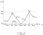
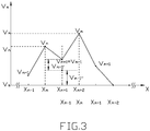
- the first and second conductive films 113, 123 are coupled electrically to each other at the touched points, and the voltages at the corresponding second electrodes 114 corresponding to the touched points rise above the first voltage (see Figs. 2 and 3 ), while the voltages at the corresponding fourth electrodes 124 corresponding to the touched points drop below the second voltage (see Figs. 4 and 5 ).
- the determination of the locations of the touched points in the first direction (Y) or in the second direction (X) will be based on one set of equations when the touched points are distant from each other, and on a different set of equations when the touched points are close to each other. Details of such determinations are as follows:
- the first location of the touched points in the second direction (X) X a is determined by one of the following equations according to a respective one of the following conditions:
- the second location of the touched points in the second direction (X) X b is determined by one of the following equations according to a respective one of the following conditions:
- the first location of the touched points in the first direction (Y) Y a is determined by one of the following equations according to a respective one of the following conditions:
- the second location of the touched points in the first direction (Y) Y b is determined by one of the following equations according to a respective one of the following conditions:
- the locations of the touched points in the first and second directions can be determined.
- Exemplary functions provided by the multi-touch detecting method are described below.
- Fig. 6 shows "zoom-in” and "zoom-out” functions provided by the multi-touch detecting method with two two-point touches on the touch panel executed sequentially at a scanning interval.
- the locations of the touched points (A, B) on the touch panel 100 on a Cartesian plane are determined to be X a , X b , Y a and Y b , on the basis of which a first rectangle can be drawn.
- the locations of the touched points (A', B') on the touch panel 100 on the Cartesian plane are determined to be X a ', X b ', Y a ' and Y b ', on the basis of which a second rectangle, enlarged in area from the first rectangle, can be drawn.
- the "zoom-in” function can be triggered by first executing the first two-point touch and then executing the second two-point touch
- the "zoom-out" function can be triggered by first executing the second two-point touch and then executing the first two-point touch.
- Fig. 7 shows a "translation" function provided by the multi-touch detecting method with two two-point touches on the touch panel executed sequentially at a scanning interval.
- the locations of the touched points (A, B) on the touch panel 100 on a Cartesian plane are determined to be X a , X b , Y a and Y b , on the basis of which a first rectangle can be drawn.
- the locations of the touched points (A', B') on the touch panel 100 on the Cartesian plane are determined to be X a ', X b ', Y a ' and Y b ', one the basis of which a second rectangle, substantially the same as and spaced apart from the first rectangle, can be drawn.
- the "translation" function can be triggered by executing the first and second two-point touches sequentially.
- Fig. 8 shows a "rotation" function provided by the multi-touch detecting method with two two-point touches on the touch panel executed sequentially at a scanning interval.
- the locations of the touched points (A, B) on the touch panel 100 on a Cartesian plane are determined to be X a , X b , Y a and Y b , on the basis of which a first rectangle can be drawn.
- the locations of the touched points (A', B') on the touch panel 100 on the Cartesian plane are determined to be X a ', X b ', Y a ' and Y b ', on the basis of which a second rectangle, substantially the same as the first rectangle and rotated 90 degrees relative to the first rectangle, can be drawn.
- the "rotation" function can be triggered by executing the first and second two-point touches sequentially.
- the structure of the touch panel 100 is simple and the multi-touch detecting method implemented by the touch panel 100 is simple.
- Circuitry in this context includes analogue and digital circuitry.
- Digital circuitry may be special purpose hardware and/or may include programmable DSP or microprocessor circuitry, provided with suitable program instructions.
Landscapes
- Engineering & Computer Science (AREA)
- General Engineering & Computer Science (AREA)
- Theoretical Computer Science (AREA)
- Human Computer Interaction (AREA)
- Physics & Mathematics (AREA)
- General Physics & Mathematics (AREA)
- Position Input By Displaying (AREA)
Description
- The present disclosure relates to a multi-touch detecting method for detecting locations of touched points on a touch panel, and more particularly to a multi-touch detecting method involving the use of at least one conductive film exhibiting electric anisotropy as a part of a touch sensor. There is also disclosed a touch device including means for implementing the detection methods.
- Touch panels are widely used in electronic products, such as mobile phones and navigation systems, for example, to serve as input devices. A new trend of touch panel technology is towards having a touch panel with multi-touch detection capability. There are several types of touch panels including resistive type, capacitive type, infrared type, and surface acoustic wave type, for example. Conventional resistive type touch panels do not support multi-touch detection. When multiple points on a resistive type touch panel are touched, the location of the touched points cannot be correctly determined. Conventional capacitive type touch panels, such as those disclosed in
U.S. Patent Application Publication Nos. 2006/0097991 and2008/0158181 EP2073109 discloses a touch panel and a display device using the same, in which a touch panel includes a first electrode plate, and a second electrode plate separated from the first electrode plate. The first electrode plate includes a first base and a first conductive layer. The first conductive layer is located on a surface of the first base. The second electrode plate includes a second base, and a second conductive layer. The second conductive layer is located on a surface of the second base. The second conductive layer is opposite to the first conductive layer. At least one of the first and second conductive layers includes a plurality of spaced carbon nanotube structures. Pressing the first electrode causes a deformation of the first electrode plate to establish an electrical connection between the first and the second conductive layers. Changes in voltages along a first direction of the first conductive layer and along a second direction of the second conductive layer can be detected by a controller to transform into coordinates of the pressing point. - According to one aspect of the present disclosure, there is provided a multi-touch detecting method adapted for detecting touched points on a touch panel.The touch panel includes first and second conductive films insulated from each other and coupled electrically to each other through touch. The first conductive film exhibits electric anisotropy, and has a lower resistivity in a first direction. The multi-touch detecting method is provided as defined in the appended
claim 1. - According to another aspect of the present disclosure, there is provided a multi-touch detecting method adapted for detecting touched points on a touch panel. The touch panel includes first and second conductive films insulated from each other and coupled electrically to each other through touch. The second conductive film exhibits electric anisotropy, and has a lower resistivity in a certain direction. The multi-touch detecting method is provided as defined by the appended claim 10 .
- The components in the drawings are not necessarily drawn to scale, the emphasis instead being placed upon clearly illustrating the principles of at least one embodiment.
-
Fig. 1 is an exploded perspective view of a touch panel in which the exemplary embodiment of a multi-touch detecting method of the present disclosure is to be implemented. -
Fig. 2 is a plot of voltages measured at measuring points of a first conductive film of the touch panel along a certain direction in response to a two-point touch in which two points on the touch panel are touched and are distant from each other in the certain direction. -
Fig. 3 is a plot of voltages measured at measuring points of the first conductive film of the touch panel along a certain direction in response to a two-point touch in which two points on the touch panel are touched and are close to each other in the certain direction. -
Fig. 4 is a plot of voltages measured at measuring points of a second conductive film of the touch panel along a certain direction in response to a two-point touch in which the two points on the touch panel are touched and are distant from each other in the certain direction. -
Fig. 5 is a plot of voltages measured at measuring points of the second conductive film of the touch panel along a certain direction in response to a two-point touch in which two points on the touch panel are touched and are close to each other in the certain direction. -
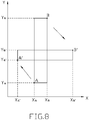
Figs. 6 to 8 are graphs schematically demonstrating how the exemplary embodiment of the multi-touch detecting method of the present disclosure is capable of supporting different exemplary multi-touch functions implemented in the touch panel. - Reference will now be made to the drawings to describe various embodiments in detail.
- Referring to
Fig. 1 , the exemplary embodiment of a multi-touch detecting method of the present disclosure is implemented in atouch panel 100. Thetouch panel 100 includes afirst layer 110, asecond layer 120, anadhesive film 130, a plurality ofspacers 132 of an insulator, and a flexible print circuit (FPC) 140. Theadhesive film 130 extends along sides of the first andsecond layers second layers recess 131 that receives theflexible print circuit 140. Thespacers 132 are disposed between the first andsecond layers second layers - The
first layer 110 includes afirst substrate 111, a firstconductive film 113, anadhesive film 112, afirst electrode 115, a plurality ofsecond electrodes 114, and a plurality ofconductive lines 116. The firstconductive film 113 is disposed on thefirst substrate 111, and is bonded securely to thefirst substrate 111 through theadhesive film 112. The firstconductive film 113 exhibits electric anisotropy, has a lower resistivity in a first direction (Y), and further has two sides (not labeled) opposite to each other in the first direction (Y). Thefirst electrode 115 is disposed at one of the sides of the firstconductive film 113, and is coupled electrically to the aforesaid one of the sides of the firstconductive film 113. Thesecond electrodes 114, such as sensing electrodes, are uniformly disposed along the other of the sides of the firstconductive film 113, and are coupled electrically to different measuring points of the other of the sides of the firstconductive film 113. Theconductive lines 116 extend respectively from the first andsecond electrodes first layer 110 in which therecess 131 of theadhesive film 130 is formed. It is noted that the number ofsecond electrodes 114 employed in the exemplary embodiment shown inFig. 1 is illustrative only and can be adjusted according to actual requirements. - The
second layer 120 includes asecond substrate 121, a secondconductive film 123, anadhesive film 122, athird electrode 126, a plurality offourth electrodes 124, and a plurality ofconductive lines 125. The secondconductive film 123 is disposed on thesecond substrate 121, is bonded securely to thesecond substrate 121 through theadhesive film 122, and is juxtaposed with the firstconductive film 113 in a face-to-face manner. The secondconductive film 123 exhibits electric anisotropy, has a lower resistivity in a second direction (X) transverse to the first direction (Y), and further has two sides (not labeled) opposite to each other in the second direction (X). Thethird electrode 126 is disposed at one of the sides of the secondconductive film 123, and is coupled electrically to the aforesaid one of the sides of the secondconductive film 123. Thefourth electrodes 124, such as sensing electrodes, are uniformly disposed along the other side of the secondconductive film 123, and are coupled electrically to different measuring points of the other of the sides of the secondconductive film 123. Theconductive lines 125 extend respectively from the third andfourth electrodes second layer 120 in which therecess 131 of theadhesive film 130 is formed. It is noted that the number offourth electrodes 124 employed in the exemplary embodiment shown inFig. 1 is illustrative only and can be adjusted according to actual requirements. - The
flexible print circuit 140 is provided with a plurality ofmetal pads 141 coupled electrically to theconductive lines conductive lines fourth electrodes - Each of the first and
second substrates adhesive films - Each of the first and second
conductive films 200920689 conductive film 113 is made from a nanomaterial that has strings of interconnected carbon nanounits, with each string substantially extending in the first direction (Y). The structure of the firstconductive film 113 permits the firstconductive film 113 to have the lower resistivity in the first direction (Y) and a higher resistivity in the second direction (X) which is 50 to 350 times greater than the lower resistivity in the first direction (Y). In other words, the firstconductive film 113 has an electric anisotropy ratio ranging from 50 to 350. The secondconductive film 123 is made from a nanomaterial that has strings of interconnected carbon nanounits, with each string substantially extending in the second direction (X). The structure of the secondconductive film 123 permits the secondconductive film 123 to have the lower resistivity in the second direction (X) and a higher resistivity in the first direction (Y) which is 50 to 350 times greater than the lower resistivity in the second direction (X). In other words, the secondconductive film 123 has an electric anisotropy ratio ranging from 50 to 350. Each of the first and secondconductive films conductive films - The exemplary embodiment of the multi-touch detecting method of the present disclosure is adapted for detecting touched points, such as the points touched by a user, on the touch panel 100, and includes: applying a first voltage to the sides of the first conductive film 113 through the first and second electrodes 115, 114, respectively; applying a second voltage greater than the first voltage to the sides of the second conductive film 123 through the third and fourth electrodes 126, 124, respectively; measuring sequentially voltages at the different measuring points of the first conductive film 113 through the second electrodes 114; obtaining a first local maximum voltage, a second local maximum voltage and a local minimum voltage from the voltages measured at the different measuring points of the first conductive film 113, the measuring point corresponding to the local minimum voltage being located between the measuring point corresponding to the first local maximum voltage and the measuring point corresponding to the second local maximum voltage; determining a first location of the touched points in the second direction (X) based on a location of the measuring point corresponding to the first local maximum voltage in the second direction (X); determining a second location of the touched points in the second direction (X) based on a location of the measuring point corresponding to the second local maximum voltage in the second direction (X); measuring sequentially voltages at the different measuring points of the second conductive film 123 through the fourth electrodes 124; obtaining a first local minimum voltage, a second local minimum voltage and a local maximum voltage from the voltages measured at the different measuring points of the second conductive film 123, the measuring point corresponding to the local maximum voltage being located between the measuring point corresponding to the first local minimum voltage and the measuring point corresponding to the second local minimum voltage; determining a first location of the touched points in the first direction (Y) based on a location of the measuring point corresponding to the first local minimum voltage in the first direction (Y); and determining a second location of the touched points in the first direction (Y) based on a location of the measuring point corresponding to the second local minimum voltage in the first direction (Y). It is noted that the exemplary embodiment is a non-limiting example and the multi-touch detecting method of the exemplary embodiment can be extended to a detection of more than two touched points.
- For example, in the measuring steps, the voltages are measured in such a manner that while each of the measuring points is measured, the first voltage is applied to the rest of the measuring points of the other of the sides of the first
conductive film 113 and the second voltage is applied to the rest of the measuring points of the other of the sides of the secondconductive film 123, in order to eliminate an adverse effect on the measuring point being measured caused by the rest of the measuring points and to thereby improve the accuracy of the measured voltage at the measuring point being measured. - When the
touch panel 100 is not touched, the first and secondconductive films second electrodes 114 are all equal to the first voltage, while the voltages measured at thefourth electrodes 124 are all equal to the second voltage. When two points on thetouch panel 100 are touched, the first and secondconductive films second electrodes 114 corresponding to the touched points rise above the first voltage (seeFigs. 2 and3 ), while the voltages at the correspondingfourth electrodes 124 corresponding to the touched points drop below the second voltage (seeFigs. 4 and5 ). - When the touched points are distant from each other, the response of the voltages at the corresponding
second electrodes 114 and the correspondingfourth electrodes 124 corresponding to the two touched points on thetouch panel 100 follows a pattern different from that of the voltages at the correspondingsecond electrodes 114 and the correspondingfourth electrodes 124 when the touched points are close to each other. Hence, the determination of the locations of the touched points in the first direction (Y) or in the second direction (X) will be based on one set of equations when the touched points are distant from each other, and on a different set of equations when the touched points are close to each other. Details of such determinations are as follows: - Referring to
Fig. 2 , in combination withFig. 1 , assuming that the first local maximum voltage Vn is measured at the nth measuring point of the firstconductive film 113, that the second local maximum voltage Vm is measured at the mth measuring point of the firstconductive film 113, and that n≥2 and m≥n+3, which represents that the touched points are distant from each other in the second direction (X), the first location of the touched points in the second direction (X) Xa is determined by one of the following equations according to a respective one of the following conditions: - if V n-1 < V n+1 , then

- if V n-1 , = V n+1, then Xa = Xn; and
- if V n-1 > V n+1, then

- In addition, the second location of the touched points in the second direction (X) Xb is determined by one of the following equations according to a respective one of the following conditions:
- if V m-1 <V m+1 , then

- if V m-1 = V m+1 , then Xb = Xm; and
- if V m-1 > V m+1 , then

- Referring to
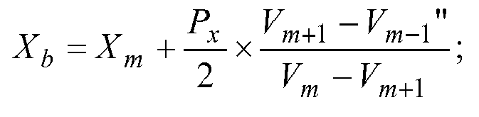
Fig. 3 , in combination withFig. 1 , assuming that m=n+2, which represents that the touched points are close to each other in the second direction (X), and that the local minimum voltage Vn+1 (=Vm-1) is measured at the n+1th, i.e., m-1th, measuring point of the first conductive film 113, and can be separated into Vn+1' and Vm-1" as functions of (Va, Vn-1, Vn, Vn+1, Vm, Vm+1) defined below, the first location of the touched points in the second direction (X) Xa and the second location of the touched points in the second direction (X) Xb are determined by the following equations according to respective ones of the following conditions:

- if V n-1 <V n+1' , then

- if V n-1 <V n+1', then Xa = Xn ;
- if V n-1 <V n+1', then

- if V m-1" <V m+1 , then

- if V m-1 <V m+1 , then Xb = Xm ; and
- if V m-1" <V m+1 , then
- Referring to
Fig. 4 , in combination withFig. 1 , assuming that the first local minimum voltage Vs is measured at the sth measuring point of the secondconductive film 123, the second local minimum voltage Vt is measured at the tth measuring point of the secondconductive film 123, and that s≥2 and t≥s+3, which represents that the touched points are distant from each other in the first direction (Y), the first location of the touched points in the first direction (Y) Ya is determined by one of the following equations according to a respective one of the following conditions: - lf V s-1 < V s+1, then

- if V s-1 = V s+1, then Ya = Ys; and
- if V s-1 > V s+1, then

- In addition, the second location of the touched points in the first direction (Y) Yb is determined by one of the following equations according to a respective one of the following conditions:
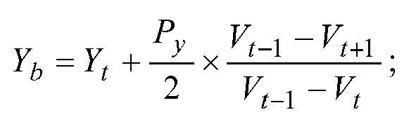
- if V t-1 < V t+1 , then

- if V t-1 = V t+1, then Yb = Yt; and
- if V t-1 > V t+1 , then
- Referring to
Fig. 5 , in combination withFig. 1 , assuming that t=s+2, which represents that the touched points are close to each other in the first direction (Y), and that the local maximum voltage Vs+1 (=Vt-1) is measured at the s+1th, i.e., t-1th, measuring point of the second conductive film 123, and can be separated into Vs+1' and Vt-1" as functions of (Vb, Vs-1, Vs, Vs+1, Vt, Vt+1) defined below, the first location of the touched points in the first direction (Y) Ya and the second location of the touched points in the first direction (Y) Yb are determined by the following equations according to respective ones of the following conditions:

- if V s-1 < Vs+1', then

- if V s-1 = Vs+1' then Ya = Ys ;
- if V s-1 > V s+1', then

- if V t-1" < V t+1, then

- if V t-1" = V t+1 , then Yb = Yt ; and
- if V t-1 " > Vt+1, then

- As described above, the locations of the touched points in the first and second directions (Y, X) can be determined. Exemplary functions provided by the multi-touch detecting method are described below.
-
Fig. 6 shows "zoom-in" and "zoom-out" functions provided by the multi-touch detecting method with two two-point touches on the touch panel executed sequentially at a scanning interval. In the first two-point touch, the locations of the touched points (A, B) on thetouch panel 100 on a Cartesian plane are determined to be Xa, Xb, Ya and Yb, on the basis of which a first rectangle can be drawn. In the second two-point touch, the locations of the touched points (A', B') on thetouch panel 100 on the Cartesian plane are determined to be Xa', Xb', Ya' and Yb', on the basis of which a second rectangle, enlarged in area from the first rectangle, can be drawn. As such, the "zoom-in" function can be triggered by first executing the first two-point touch and then executing the second two-point touch, and the "zoom-out" function can be triggered by first executing the second two-point touch and then executing the first two-point touch. -
Fig. 7 shows a "translation" function provided by the multi-touch detecting method with two two-point touches on the touch panel executed sequentially at a scanning interval. In the first two-point touch, the locations of the touched points (A, B) on thetouch panel 100 on a Cartesian plane are determined to be Xa, Xb, Ya and Yb, on the basis of which a first rectangle can be drawn. In the second two-point touch, the locations of the touched points (A', B') on thetouch panel 100 on the Cartesian plane are determined to be Xa', Xb', Ya' and Yb', one the basis of which a second rectangle, substantially the same as and spaced apart from the first rectangle, can be drawn. As such, the "translation" function can be triggered by executing the first and second two-point touches sequentially. -
Fig. 8 shows a "rotation" function provided by the multi-touch detecting method with two two-point touches on the touch panel executed sequentially at a scanning interval. In the first two-point touch, the locations of the touched points (A, B) on thetouch panel 100 on a Cartesian plane are determined to be Xa, Xb, Ya and Yb, on the basis of which a first rectangle can be drawn. In the second two-point touch, the locations of the touched points (A', B') on thetouch panel 100 on the Cartesian plane are determined to be Xa', Xb', Ya' and Yb', on the basis of which a second rectangle, substantially the same as the first rectangle and rotated 90 degrees relative to the first rectangle, can be drawn. As such, the "rotation" function can be triggered by executing the first and second two-point touches sequentially. - In sum, with the use of the first and second
conductive films touch panel 100 is simple and the multi-touch detecting method implemented by thetouch panel 100 is simple. - The steps of all the methods described above will be performed by signal processing circuitry included in a touch screen device incorporating the panel, or by separate circuitry. Circuitry in this context includes analogue and digital circuitry. Digital circuitry may be special purpose hardware and/or may include programmable DSP or microprocessor circuitry, provided with suitable program instructions.
- It is to be understood that even though numerous characteristics and advantages of the present embodiments have been set forth in the foregoing description, together with details of the structures and functions of the embodiments, the disclosure is illustrative only; and that changes may be made in detail, especially in matters of shape, size, and arrangement of parts, within the principles of the embodiments, to the full extent indicated by the broad general meaning of the terms in which the appended claims are expressed. Moreover the claims may be expanded to claim the touch device including means for implementing the respective steps of the methods presently claimed.
Claims (12)
- A multi-touch detecting method adapted for detecting touched points on a touch panel (100), the touch panel (100) including first and second conductive films (113, 123) insulated from each other and coupled electrically to each other through touch, the first conductive film (113) exhibiting electric anisotropy, and having a lower resistivity in a first direction (Y), the multi-touch detecting method comprising:applying a first voltage Va to the first conductive film (113);applying a second voltage Vb greater than the first voltage Va to the second conductive film (123); the multi-touch detecting method characterised by further comprising:obtaining a first local maximum voltage Vn' a second local maximum voltage Vm and a local minimum voltage from voltages measured at a plurality of different measuring points of the first conductive film (113), the measuring point corresponding to the local minimum voltage being located between the measuring point corresponding to the first local maximum voltage and the measuring point corresponding to the second local maximum voltage;determining a first location of the touched points Xa in a second direction (X) transverse to the first direction (Y) based on a location of the measuring point corresponding to the first local maximum voltage in the second direction (X); anddetermining a second location of the touched points Xb in the second direction (X) based on a location of the measuring point corresponding to the second local maximum voltage in the second direction (X);wherein the first local maximum voltage Vn is measured at the nth measuring point, the second local maximum voltage Vm being measured at the mth measuring point, and wherein in a case where n≥2, m=n+2, the first location of the touched points Xa and the second location of the touched points Xb are determined by the following equations according to respective ones of the following conditions:let
 let
let if V n-1 < V n+1', then
 if V n-1 = V n+1' , then Xa = Xn ;if V n-1=V n+1', then
 if V m-1" = V m+1, then
 if V m-1" = V m+1' then Xb = Xm ; andif V n-1" > V m+1, then
 where Va is the first voltage, Vn-1 is the voltage measured at the n-1th measuring point, Vn+1 is the voltage measured at the n+1th measuring point, Vm+1 is the voltage measured at the m+1th measuring point, Xn is the location of the nth measuring point in the second direction, Xm is the location of the mth measuring point in the second direction, and Px is a distance between two adjacent ones of the measuring points.
 - The multi-touch detecting method of claim 1, wherein the voltages are measured in such a manner that while each of the plurality of measuring points is measured, the first voltage Va is applied to the rest of the plurality of measuring points.
- The multi-touch detecting method of claim 1 or 2, wherein in a case where n≥2 and m≥n+3, the first location of the touched points Xa is determined by one of the following equations according to a respective one of the following conditions:if V n-1<V n+1 , then
 if V n-1 = V n+1, then Xa = Xn; andif V n-1 > V n+1 , thenwhere Vn-1 is the voltage measured at the n-1th measuring point, Vn+1 is the voltage measured at the n+1th measuring point, Xn is the location of the nth measuring point in the second direction (X), and Px is a distance between two adjacent ones of the measuring points.
- The multi-touch detecting method of claim 3, wherein in a case where n≥2 and m≥n+3 the second location of the touched points Xb is determined by one of the following equations according to a respective one of the following conditions:if V m-1 < V m+1, then
 if V m-1 < V m+1 = V m+1 , then Xb = Xm; andif V m-1 > V m+1, thenwhere Vm-1 is the voltage measured at the m-1th measuring point, Vm+1 is the voltage measured at the m+1th measuring point, and Xm is the location of the mth measuring point in the second direction (X).
- The multi-touch detecting method of any preceding claim, the second conductive film (123) exhibiting electric anisotropy, and having a lower resistivity in the second direction (X), the multi-touch detecting method further comprising:measuring sequentially voltages at a plurality of different measuring points of the second conductive film (123);obtaining a first local minimum voltage Vs, a second local minimum voltage Vt and a local maximum voltage from the voltages measured at the different measuring points of the second conductive film (123), the measuring point corresponding to the local maximum voltage being located between the measuring point corresponding to the first local minimum voltage and the measuring point corresponding to the second local minimum voltage;determining a first location of the touched points Ya in the first direction (Y) based on a location of the measuring point corresponding to the first local minimum voltage in the first direction (Y); anddetermining a second location of the touched Yb in the first direction (Y) based on a location of the measuring point corresponding to the second local minimum voltage in the first direction (Y).
- The multi-touch detecting method of claim 5, wherein the voltages measured at the different measuring points of the second conductive film are measured in such a manner that while each of the plurality of measuring points is measured, the second voltage is applied to the rest of the plurality of measuring points.
- The multi-touch detecting method of claim 5 or 6, wherein the first local minimum voltage Vs is measured at the sth measuring point of the second conductive film (123), wherein in a case where s≥2 and t≥s+3, the first location Ya of the touched points in the first direction (Y) is determined by one of the following equations according to a respective one of the following conditions:if V s-1 < V s+1, then
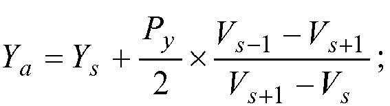 if V s-1 = V s+1, then Ya = Ys ; andof V s-1 > V s+1 , thenwhere Vs-1 is the voltage measured at the s-1th measuring point of the second conductive film (123), Vs+1 is the voltage measured at the s+1th measuring point of the second conductive film (123), Ys is the location of the sth measuring point of the second conductive film (123) in the first direction, and Py is a distance between two adjacent ones of the measuring points of the second conductive film (123).
- The multi-touch detecting method of claim 7, wherein the second local minimum voltage Vt is measured at the tth measuring point of the second conductive film (123), wherein in a case where s≥2 and t≥s+3, the second location Yb of the touched points in the first direction (Y) is determined by one of the following equations according to a respective one of the following conditions:if V t-1 < V t+1, then
 if V t-1 = V t+1, then Yb = Yt; andif Vt-1 > V t+1, thenwhere Vt-1 is the voltage measured at the t-1th measuring point of the second conductive film (123), Vt+1 is the voltage measured at the t+1th measuring point of the second conductive film (123), and Yt is the location of the tth measuring point of the second conductive film (123) in the first direction (Y).
- The multi-touch detecting method of claim 5 or 6, wherein the first local minimum voltage Vs is measured at the sth measuring point of the second conductive film (123), the second local minimum voltage Vt being measured at the tth measuring point of the second conductive film (123), wherein in a case where s≥2, t=s+2, the first location Ya of the touched points in the first direction (Y) and the second location Yb of the touched points in the first direction (Y) are determined by the following equations according to respective ones of the following conditions:let
 let
let if V s-1 < V s+1', then
 if V s-1 = V s+1 ', then Ya = Ys ;if V s-1 > V s+1 ' then
 if V t-1" < V t+1, then
 if V t-1 " = V t+1, then Yb = Yt ; andif V t-1" > V t+1, thenwhere Vb is the second voltage, Vs-1 is the voltage measured at the s-1th measuring point of the second conductive film (123), Vs+1 is the voltage measured at the s+1th measuring point of the second conductive film (123), Vt+1 is the voltage measured at the t+1th measuring point of the second conductive film (123), Ys is the location of the sth measuring point of the second conductive film (123) in the first direction, Yt is the location of the tth measuring point of the second conductive film (123) in the first direction (Y), and Py is a distance between two adjacent ones of the measuring points of the second conductive film (123).
- A multi-touch detecting method adapted for detecting touched points on a touch panel, the touch panel including first and second conductive films (113, 123) insulated from each other and coupled electrically to each other through touch, the second conductive film exhibiting electric anisotropy, and having a lower resistivity in a certain direction, the multi-touch detecting method comprising:applying a first voltage Va to the first conductive film (113);applying a second voltage Vb greater than the first voltage Va to the second conductive film (123);measuring sequentially voltages at different measuring points of the second conductive film (123); the multi-touch detecting method characterised by further comprising:obtaining a first local minimum voltage Vs, a second local minimum voltage Vt and a local maximum voltage from the voltages measured at the different measuring points of the second conductive film (123), the measuring point corresponding to the local maximum voltage being located between the measuring point corresponding to the first local minimum voltage and the measuring point corresponding to the second local minimum voltage;determining a first location of the touched points Ya based on a location of the measuring point corresponding to the first local minimum voltage; anddetermining a second location of the touched points Yb based on a location of the measuring point corresponding to the second local minimum voltage;wherein the first local minimum voltage Vs is measured at the sth measuring point, the second local minimum voltage Vt being measured at the tth measuring point, wherein in a case where s≥2, t=s+2, the first location of the touched points Ya and the second location of the touched points Yb are determined by the following equations according to respective ones of the following conditions:let
 let
let if V s-1< V s+1', then
 if V s-1=V s+1', then Ya = Ys ;if V s-1 > V s+1', then
 if V t-1" < V t+1, then
 if V t-1" = V t+1, then Yb = Yt ; andif V t-1">V t+1, then
 where Vb is the second voltage, Vs-1 is the voltage measured at the s-1th measuring point, Vs+1 is the voltage measured at the s+1th measuring point, Vt+1 is the voltage measured at the t+1th measuring point, Ys is the location of the sth measuring point, Yt is the location of the tth measuring point, and Py is a distance between two adjacent ones of the measuring points.
 - The multi-touch detecting method of claim 10, wherein the first local minimum voltage Vs is measured at the sth measuring point, wherein in a case where s≥2 and t≥s+3, the first location of the touched points Ya is determined by one of the following equations according to a respective one of the following conditions:if V s-1 < V s+1, then
 if V s-1 = V s+1 , then Ya = Ys ; andif V s-1 > V s+1 , thenwhere Vs-1 is the voltage measured at the s-1th measuring point, Vs+1 is the voltage measured at the s+1h measuring point, Ys is the location of the sth measuring point, and Py is a distance between two adjacent ones of the measuring points.
- The multi-touch detecting method of claim 11, wherein the second local minimum voltage Vt is measured at the tth measuring point, wherein in a case where s≥2 and t≥s+3, the second location of the touched points Yb is determined by one of the following equations according to a respective one of the following conditions:if V t-1 < V t+1, then
 if V t-1 = V t+1, then Yb = Yt ; andif V t-1 > V t+1, thenwhere Vt-1 is the voltage measured at the t-1th measuring point, Vt+1 is the voltage measured at the t+1th measuring point, and Yt is the location of the tth measuring point.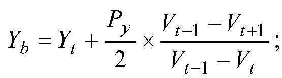
Applications Claiming Priority (1)
| Application Number | Priority Date | Filing Date | Title |
|---|---|---|---|
| CN2009103042429A CN101950212B (en) | 2009-07-10 | 2009-07-10 | Multipoint identification method for touch screen |
Publications (3)
| Publication Number | Publication Date |
|---|---|
| EP2273356A2 EP2273356A2 (en) | 2011-01-12 |
| EP2273356A3 EP2273356A3 (en) | 2012-11-07 |
| EP2273356B1 true EP2273356B1 (en) | 2017-09-06 |
Family
ID=42797440
Family Applications (1)
| Application Number | Title | Priority Date | Filing Date |
|---|---|---|---|
| EP10168940.4A Active EP2273356B1 (en) | 2009-07-10 | 2010-07-08 | Multi-touch detecting method for detecting locations of touched points on a touch panel |
Country Status (5)
| Country | Link |
|---|---|
| US (1) | US8564542B2 (en) |
| EP (1) | EP2273356B1 (en) |
| JP (1) | JP5723547B2 (en) |
| KR (1) | KR20110005642A (en) |
| CN (1) | CN101950212B (en) |
Families Citing this family (10)
| Publication number | Priority date | Publication date | Assignee | Title |
|---|---|---|---|---|
| TW201310470A (en) * | 2011-08-31 | 2013-03-01 | Shih Hua Technology Ltd | Transparent conductive film and touch panel using the same |
| TW201335669A (en) * | 2012-02-20 | 2013-09-01 | Innocom Tech Shenzhen Co Ltd | Touch control display apparatus and manufacturing method thereof |
| US8823664B2 (en) | 2012-02-24 | 2014-09-02 | Cypress Semiconductor Corporation | Close touch detection and tracking |
| KR102097696B1 (en) * | 2012-08-27 | 2020-04-06 | 삼성전자주식회사 | Method of controlling touch function and an electronic device thereof |
| JP6249652B2 (en) | 2012-08-27 | 2017-12-20 | 三星電子株式会社Samsung Electronics Co.,Ltd. | Touch function control method and electronic device thereof |
| US20140062917A1 (en) * | 2012-08-29 | 2014-03-06 | Samsung Electronics Co., Ltd. | Method and apparatus for controlling zoom function in an electronic device |
| TW201433938A (en) | 2013-02-19 | 2014-09-01 | Pixart Imaging Inc | Virtual navigation apparatus, navigation method, and computer program product thereof |
| CN104007849B (en) * | 2013-02-26 | 2017-09-22 | 原相科技股份有限公司 | Virtual navigation device and navigation method thereof |
| CN104553113A (en) * | 2014-12-11 | 2015-04-29 | 业成光电(深圳)有限公司 | Acoustic wave fingerprint identification component and manufacturing method thereof |
| CN105242816B (en) * | 2015-07-28 | 2021-08-06 | 合肥工业大学 | A multi-touch system based on resistive screen |
Family Cites Families (14)
| Publication number | Priority date | Publication date | Assignee | Title |
|---|---|---|---|---|
| US5825352A (en) * | 1996-01-04 | 1998-10-20 | Logitech, Inc. | Multiple fingers contact sensing method for emulating mouse buttons and mouse operations on a touch sensor pad |
| US7663607B2 (en) | 2004-05-06 | 2010-02-16 | Apple Inc. | Multipoint touchscreen |
| KR100451773B1 (en) * | 2002-11-20 | 2004-10-08 | 엘지.필립스 엘시디 주식회사 | Touch Panel in Digital Resistive Type |
| US20050209392A1 (en) | 2003-12-17 | 2005-09-22 | Jiazhong Luo | Polymer binders for flexible and transparent conductive coatings containing carbon nanotubes |
| JP5194339B2 (en) * | 2005-06-29 | 2013-05-08 | カシオ計算機株式会社 | Liquid crystal display element |
| US8026903B2 (en) | 2007-01-03 | 2011-09-27 | Apple Inc. | Double-sided touch sensitive panel and flex circuit bonding |
| CN100582875C (en) * | 2007-04-13 | 2010-01-20 | 群康科技(深圳)有限公司 | Touch screen display apparatus |
| US8355009B2 (en) * | 2007-04-25 | 2013-01-15 | Mcdermid William J | Method and apparatus for determining coordinates of simultaneous touches on a touch sensor pad |
| TWI346086B (en) | 2007-11-09 | 2011-08-01 | Hon Hai Prec Ind Co Ltd | Apparatus and method for synthesizing films of carbon nanotubes |
| EP2073109A3 (en) * | 2007-12-21 | 2012-08-22 | Tsing Hua University | Touch panel and display device using the same |
| US20090174675A1 (en) * | 2008-01-09 | 2009-07-09 | Dave Gillespie | Locating multiple objects on a capacitive touch pad |
| CN101943967B (en) * | 2009-07-08 | 2012-08-15 | 群康科技(深圳)有限公司 | Method for positioning touch screen |
| CN101950213B (en) * | 2009-07-10 | 2013-05-22 | 群康科技(深圳)有限公司 | Touch screen and multi-point identification method used for same |
| US8427444B2 (en) * | 2010-04-12 | 2013-04-23 | Silicon Integrated Systems Corp. | Ghost cancellation method for multi-touch sensitive device |
-
2009
- 2009-07-10 CN CN2009103042429A patent/CN101950212B/en active Active
-
2010
- 2010-06-29 US US12/826,585 patent/US8564542B2/en not_active Expired - Fee Related
- 2010-07-02 KR KR1020100063891A patent/KR20110005642A/en not_active Withdrawn
- 2010-07-08 EP EP10168940.4A patent/EP2273356B1/en active Active
- 2010-07-08 JP JP2010155685A patent/JP5723547B2/en active Active
Non-Patent Citations (1)
| Title |
|---|
| None * |
Also Published As
| Publication number | Publication date |
|---|---|
| CN101950212B (en) | 2012-05-23 |
| US20110007027A1 (en) | 2011-01-13 |
| US8564542B2 (en) | 2013-10-22 |
| CN101950212A (en) | 2011-01-19 |
| EP2273356A2 (en) | 2011-01-12 |
| KR20110005642A (en) | 2011-01-18 |
| EP2273356A3 (en) | 2012-11-07 |
| JP5723547B2 (en) | 2015-05-27 |
| JP2011018335A (en) | 2011-01-27 |
Similar Documents
| Publication | Publication Date | Title |
|---|---|---|
| EP2273356A2 (en) | Multi-touch detecting method for detecting locations of touched points on a touch panel | |
| US9304630B2 (en) | Touch panel | |
| US10901565B2 (en) | Portable computer | |
| CN100485597C (en) | Force imaging input device and system | |
| EP2275909A2 (en) | Touch panel and detecting method thereof | |
| US9077793B2 (en) | Carbon nanotube based flexible mobile phone | |
| JP4763848B2 (en) | Touch panel and display device | |
| US20110273396A1 (en) | Touch screen device | |
| KR101501940B1 (en) | Touch screen and manufacturing method thereof | |
| JP6030220B2 (en) | Touch panel and manufacturing method thereof | |
| US20140293151A1 (en) | Touch Panel and Manufacturing Method Thereof | |
| KR20100036907A (en) | Dual-side integrated touch panel structure | |
| US20090079708A1 (en) | Three-wire resistive touch panel and display device using same | |
| KR20140047936A (en) | Touch panel and method for manufacturing the same | |
| US20140145975A1 (en) | Touchscreen device and screen zoom method thereof | |
| TW201516774A (en) | Method of determining touch point and touch pressure | |
| US20140043252A1 (en) | Touchscreen panel and touchscreen device | |
| US20140253826A1 (en) | Touch screen and manufacturing method thereof | |
| TWI465992B (en) | Method for detecting touch spot of touch panel | |
| US8400421B2 (en) | Touch panel and multi-touch detecting method thereof | |
| CN107239173B (en) | Touch device, touch display device and driving method thereof | |
| US20140253824A1 (en) | Touch panel and manufacturing method thereof | |
| US9958999B2 (en) | Capacitive touch sensor with Z-shaped electrode pattern | |
| KR101184459B1 (en) | Pressure sensor | |
| US20140062915A1 (en) | Touchscreen panel and touchscreen device |
Legal Events
| Date | Code | Title | Description |
|---|---|---|---|
| PUAI | Public reference made under article 153(3) epc to a published international application that has entered the european phase |
Free format text: ORIGINAL CODE: 0009012 |
|
| AK | Designated contracting states |
Kind code of ref document: A2 Designated state(s): AL AT BE BG CH CY CZ DE DK EE ES FI FR GB GR HR HU IE IS IT LI LT LU LV MC MK MT NL NO PL PT RO SE SI SK SM TR |
|
| AX | Request for extension of the european patent |
Extension state: BA ME RS |
|
| PUAL | Search report despatched |
Free format text: ORIGINAL CODE: 0009013 |
|
| AK | Designated contracting states |
Kind code of ref document: A3 Designated state(s): AL AT BE BG CH CY CZ DE DK EE ES FI FR GB GR HR HU IE IS IT LI LT LU LV MC MK MT NL NO PL PT RO SE SI SK SM TR |
|
| AX | Request for extension of the european patent |
Extension state: BA ME RS |
|
| RIC1 | Information provided on ipc code assigned before grant |
Ipc: G06F 3/041 20060101ALI20121001BHEP Ipc: G06F 3/045 20060101AFI20121001BHEP |
|
| 17P | Request for examination filed |
Effective date: 20130506 |
|
| GRAP | Despatch of communication of intention to grant a patent |
Free format text: ORIGINAL CODE: EPIDOSNIGR1 |
|
| RAP1 | Party data changed (applicant data changed or rights of an application transferred) |
Owner name: INNOLUX CORPORATION |
|
| INTG | Intention to grant announced |
Effective date: 20170328 |
|
| GRAS | Grant fee paid |
Free format text: ORIGINAL CODE: EPIDOSNIGR3 |
|
| GRAA | (expected) grant |
Free format text: ORIGINAL CODE: 0009210 |
|
| AK | Designated contracting states |
Kind code of ref document: B1 Designated state(s): AL AT BE BG CH CY CZ DE DK EE ES FI FR GB GR HR HU IE IS IT LI LT LU LV MC MK MT NL NO PL PT RO SE SI SK SM TR |
|
| REG | Reference to a national code |
Ref country code: GB Ref legal event code: FG4D |
|
| REG | Reference to a national code |
Ref country code: CH Ref legal event code: EP Ref country code: AT Ref legal event code: REF Ref document number: 926543 Country of ref document: AT Kind code of ref document: T Effective date: 20170915 |
|
| REG | Reference to a national code |
Ref country code: IE Ref legal event code: FG4D |
|
| REG | Reference to a national code |
Ref country code: DE Ref legal event code: R096 Ref document number: 602010044958 Country of ref document: DE |
|
| REG | Reference to a national code |
Ref country code: NL Ref legal event code: MP Effective date: 20170906 |
|
| REG | Reference to a national code |
Ref country code: LT Ref legal event code: MG4D |
|
| PG25 | Lapsed in a contracting state [announced via postgrant information from national office to epo] |
Ref country code: LT Free format text: LAPSE BECAUSE OF FAILURE TO SUBMIT A TRANSLATION OF THE DESCRIPTION OR TO PAY THE FEE WITHIN THE PRESCRIBED TIME-LIMIT Effective date: 20170906 Ref country code: NO Free format text: LAPSE BECAUSE OF FAILURE TO SUBMIT A TRANSLATION OF THE DESCRIPTION OR TO PAY THE FEE WITHIN THE PRESCRIBED TIME-LIMIT Effective date: 20171206 Ref country code: HR Free format text: LAPSE BECAUSE OF FAILURE TO SUBMIT A TRANSLATION OF THE DESCRIPTION OR TO PAY THE FEE WITHIN THE PRESCRIBED TIME-LIMIT Effective date: 20170906 Ref country code: SE Free format text: LAPSE BECAUSE OF FAILURE TO SUBMIT A TRANSLATION OF THE DESCRIPTION OR TO PAY THE FEE WITHIN THE PRESCRIBED TIME-LIMIT Effective date: 20170906 Ref country code: FI Free format text: LAPSE BECAUSE OF FAILURE TO SUBMIT A TRANSLATION OF THE DESCRIPTION OR TO PAY THE FEE WITHIN THE PRESCRIBED TIME-LIMIT Effective date: 20170906 |
|
| REG | Reference to a national code |
Ref country code: AT Ref legal event code: MK05 Ref document number: 926543 Country of ref document: AT Kind code of ref document: T Effective date: 20170906 |
|
| PG25 | Lapsed in a contracting state [announced via postgrant information from national office to epo] |
Ref country code: ES Free format text: LAPSE BECAUSE OF FAILURE TO SUBMIT A TRANSLATION OF THE DESCRIPTION OR TO PAY THE FEE WITHIN THE PRESCRIBED TIME-LIMIT Effective date: 20170906 Ref country code: LV Free format text: LAPSE BECAUSE OF FAILURE TO SUBMIT A TRANSLATION OF THE DESCRIPTION OR TO PAY THE FEE WITHIN THE PRESCRIBED TIME-LIMIT Effective date: 20170906 Ref country code: BG Free format text: LAPSE BECAUSE OF FAILURE TO SUBMIT A TRANSLATION OF THE DESCRIPTION OR TO PAY THE FEE WITHIN THE PRESCRIBED TIME-LIMIT Effective date: 20171206 Ref country code: GR Free format text: LAPSE BECAUSE OF FAILURE TO SUBMIT A TRANSLATION OF THE DESCRIPTION OR TO PAY THE FEE WITHIN THE PRESCRIBED TIME-LIMIT Effective date: 20171207 |
|
| PG25 | Lapsed in a contracting state [announced via postgrant information from national office to epo] |
Ref country code: NL Free format text: LAPSE BECAUSE OF FAILURE TO SUBMIT A TRANSLATION OF THE DESCRIPTION OR TO PAY THE FEE WITHIN THE PRESCRIBED TIME-LIMIT Effective date: 20170906 |
|
| PG25 | Lapsed in a contracting state [announced via postgrant information from national office to epo] |
Ref country code: PL Free format text: LAPSE BECAUSE OF FAILURE TO SUBMIT A TRANSLATION OF THE DESCRIPTION OR TO PAY THE FEE WITHIN THE PRESCRIBED TIME-LIMIT Effective date: 20170906 Ref country code: RO Free format text: LAPSE BECAUSE OF FAILURE TO SUBMIT A TRANSLATION OF THE DESCRIPTION OR TO PAY THE FEE WITHIN THE PRESCRIBED TIME-LIMIT Effective date: 20170906 Ref country code: CZ Free format text: LAPSE BECAUSE OF FAILURE TO SUBMIT A TRANSLATION OF THE DESCRIPTION OR TO PAY THE FEE WITHIN THE PRESCRIBED TIME-LIMIT Effective date: 20170906 |
|
| PG25 | Lapsed in a contracting state [announced via postgrant information from national office to epo] |
Ref country code: AT Free format text: LAPSE BECAUSE OF FAILURE TO SUBMIT A TRANSLATION OF THE DESCRIPTION OR TO PAY THE FEE WITHIN THE PRESCRIBED TIME-LIMIT Effective date: 20170906 Ref country code: IS Free format text: LAPSE BECAUSE OF FAILURE TO SUBMIT A TRANSLATION OF THE DESCRIPTION OR TO PAY THE FEE WITHIN THE PRESCRIBED TIME-LIMIT Effective date: 20180106 Ref country code: SK Free format text: LAPSE BECAUSE OF FAILURE TO SUBMIT A TRANSLATION OF THE DESCRIPTION OR TO PAY THE FEE WITHIN THE PRESCRIBED TIME-LIMIT Effective date: 20170906 Ref country code: IT Free format text: LAPSE BECAUSE OF FAILURE TO SUBMIT A TRANSLATION OF THE DESCRIPTION OR TO PAY THE FEE WITHIN THE PRESCRIBED TIME-LIMIT Effective date: 20170906 Ref country code: SM Free format text: LAPSE BECAUSE OF FAILURE TO SUBMIT A TRANSLATION OF THE DESCRIPTION OR TO PAY THE FEE WITHIN THE PRESCRIBED TIME-LIMIT Effective date: 20170906 Ref country code: EE Free format text: LAPSE BECAUSE OF FAILURE TO SUBMIT A TRANSLATION OF THE DESCRIPTION OR TO PAY THE FEE WITHIN THE PRESCRIBED TIME-LIMIT Effective date: 20170906 |
|
| REG | Reference to a national code |
Ref country code: DE Ref legal event code: R097 Ref document number: 602010044958 Country of ref document: DE |
|
| REG | Reference to a national code |
Ref country code: FR Ref legal event code: PLFP Year of fee payment: 9 |
|
| PLBE | No opposition filed within time limit |
Free format text: ORIGINAL CODE: 0009261 |
|
| STAA | Information on the status of an ep patent application or granted ep patent |
Free format text: STATUS: NO OPPOSITION FILED WITHIN TIME LIMIT |
|
| PG25 | Lapsed in a contracting state [announced via postgrant information from national office to epo] |
Ref country code: DK Free format text: LAPSE BECAUSE OF FAILURE TO SUBMIT A TRANSLATION OF THE DESCRIPTION OR TO PAY THE FEE WITHIN THE PRESCRIBED TIME-LIMIT Effective date: 20170906 |
|
| 26N | No opposition filed |
Effective date: 20180607 |
|
| PG25 | Lapsed in a contracting state [announced via postgrant information from national office to epo] |
Ref country code: SI Free format text: LAPSE BECAUSE OF FAILURE TO SUBMIT A TRANSLATION OF THE DESCRIPTION OR TO PAY THE FEE WITHIN THE PRESCRIBED TIME-LIMIT Effective date: 20170906 |
|
| REG | Reference to a national code |
Ref country code: CH Ref legal event code: PL |
|
| PG25 | Lapsed in a contracting state [announced via postgrant information from national office to epo] |
Ref country code: MC Free format text: LAPSE BECAUSE OF FAILURE TO SUBMIT A TRANSLATION OF THE DESCRIPTION OR TO PAY THE FEE WITHIN THE PRESCRIBED TIME-LIMIT Effective date: 20170906 Ref country code: LU Free format text: LAPSE BECAUSE OF NON-PAYMENT OF DUE FEES Effective date: 20180708 |
|
| REG | Reference to a national code |
Ref country code: BE Ref legal event code: MM Effective date: 20180731 |
|
| REG | Reference to a national code |
Ref country code: IE Ref legal event code: MM4A |
|
| PG25 | Lapsed in a contracting state [announced via postgrant information from national office to epo] |
Ref country code: LI Free format text: LAPSE BECAUSE OF NON-PAYMENT OF DUE FEES Effective date: 20180731 Ref country code: CH Free format text: LAPSE BECAUSE OF NON-PAYMENT OF DUE FEES Effective date: 20180731 Ref country code: IE Free format text: LAPSE BECAUSE OF NON-PAYMENT OF DUE FEES Effective date: 20180708 |
|
| PG25 | Lapsed in a contracting state [announced via postgrant information from national office to epo] |
Ref country code: BE Free format text: LAPSE BECAUSE OF NON-PAYMENT OF DUE FEES Effective date: 20180731 |
|
| REG | Reference to a national code |
Ref country code: DE Ref legal event code: R082 Ref document number: 602010044958 Country of ref document: DE Representative=s name: STRAUS, ALEXANDER, DIPL.-CHEM.UNIV. DR.PHIL., DE Ref country code: DE Ref legal event code: R082 Ref document number: 602010044958 Country of ref document: DE Representative=s name: 2K PATENT- UND RECHTSANWAELTE PARTNERSCHAFT MB, DE |
|
| PG25 | Lapsed in a contracting state [announced via postgrant information from national office to epo] |
Ref country code: MT Free format text: LAPSE BECAUSE OF NON-PAYMENT OF DUE FEES Effective date: 20180708 |
|
| PG25 | Lapsed in a contracting state [announced via postgrant information from national office to epo] |
Ref country code: TR Free format text: LAPSE BECAUSE OF FAILURE TO SUBMIT A TRANSLATION OF THE DESCRIPTION OR TO PAY THE FEE WITHIN THE PRESCRIBED TIME-LIMIT Effective date: 20170906 |
|
| PG25 | Lapsed in a contracting state [announced via postgrant information from national office to epo] |
Ref country code: HU Free format text: LAPSE BECAUSE OF FAILURE TO SUBMIT A TRANSLATION OF THE DESCRIPTION OR TO PAY THE FEE WITHIN THE PRESCRIBED TIME-LIMIT; INVALID AB INITIO Effective date: 20100708 Ref country code: PT Free format text: LAPSE BECAUSE OF FAILURE TO SUBMIT A TRANSLATION OF THE DESCRIPTION OR TO PAY THE FEE WITHIN THE PRESCRIBED TIME-LIMIT Effective date: 20170906 |
|
| PG25 | Lapsed in a contracting state [announced via postgrant information from national office to epo] |
Ref country code: MK Free format text: LAPSE BECAUSE OF NON-PAYMENT OF DUE FEES Effective date: 20170906 Ref country code: CY Free format text: LAPSE BECAUSE OF FAILURE TO SUBMIT A TRANSLATION OF THE DESCRIPTION OR TO PAY THE FEE WITHIN THE PRESCRIBED TIME-LIMIT Effective date: 20170906 |
|
| PG25 | Lapsed in a contracting state [announced via postgrant information from national office to epo] |
Ref country code: AL Free format text: LAPSE BECAUSE OF FAILURE TO SUBMIT A TRANSLATION OF THE DESCRIPTION OR TO PAY THE FEE WITHIN THE PRESCRIBED TIME-LIMIT Effective date: 20170906 |
|
| REG | Reference to a national code |
Ref country code: DE Ref legal event code: R082 Ref document number: 602010044958 Country of ref document: DE Representative=s name: STRAUS, ALEXANDER, DIPL.-CHEM.UNIV. DR.PHIL., DE |
|
| PGFP | Annual fee paid to national office [announced via postgrant information from national office to epo] |
Ref country code: GB Payment date: 20250626 Year of fee payment: 16 |
|
| PGFP | Annual fee paid to national office [announced via postgrant information from national office to epo] |
Ref country code: DE Payment date: 20250702 Year of fee payment: 16 |
|
| PGFP | Annual fee paid to national office [announced via postgrant information from national office to epo] |
Ref country code: FR Payment date: 20250703 Year of fee payment: 16 |