EP2273286A2 - Radiation image detection apparatus and manufacturing method of the same - Google Patents
Radiation image detection apparatus and manufacturing method of the same Download PDFInfo
- Publication number
- EP2273286A2 EP2273286A2 EP10168292A EP10168292A EP2273286A2 EP 2273286 A2 EP2273286 A2 EP 2273286A2 EP 10168292 A EP10168292 A EP 10168292A EP 10168292 A EP10168292 A EP 10168292A EP 2273286 A2 EP2273286 A2 EP 2273286A2
- Authority
- EP
- European Patent Office
- Prior art keywords
- scintillator
- detection apparatus
- image detection
- radiation image
- radiation
- Prior art date
- Legal status (The legal status is an assumption and is not a legal conclusion. Google has not performed a legal analysis and makes no representation as to the accuracy of the status listed.)
- Ceased
Links
Images



Classifications
-
- G—PHYSICS
- G01—MEASURING; TESTING
- G01T—MEASUREMENT OF NUCLEAR OR X-RADIATION
- G01T1/00—Measuring X-radiation, gamma radiation, corpuscular radiation, or cosmic radiation
- G01T1/16—Measuring radiation intensity
- G01T1/20—Measuring radiation intensity with scintillation detectors
- G01T1/2018—Scintillation-photodiode combinations
- G01T1/20186—Position of the photodiode with respect to the incoming radiation, e.g. in the front of, below or sideways the scintillator
-
- G—PHYSICS
- G01—MEASURING; TESTING
- G01T—MEASUREMENT OF NUCLEAR OR X-RADIATION
- G01T1/00—Measuring X-radiation, gamma radiation, corpuscular radiation, or cosmic radiation
- G01T1/16—Measuring radiation intensity
- G01T1/20—Measuring radiation intensity with scintillation detectors
- G01T1/2018—Scintillation-photodiode combinations
- G01T1/20185—Coupling means between the photodiode and the scintillator, e.g. optical couplings using adhesives with wavelength-shifting fibres
-
- G—PHYSICS
- G01—MEASURING; TESTING
- G01T—MEASUREMENT OF NUCLEAR OR X-RADIATION
- G01T1/00—Measuring X-radiation, gamma radiation, corpuscular radiation, or cosmic radiation
- G01T1/16—Measuring radiation intensity
- G01T1/20—Measuring radiation intensity with scintillation detectors
- G01T1/2018—Scintillation-photodiode combinations
- G01T1/20187—Position of the scintillator with respect to the photodiode, e.g. photodiode surrounding the crystal, the crystal surrounding the photodiode, shape or size of the scintillator
-
- G—PHYSICS
- G01—MEASURING; TESTING
- G01T—MEASUREMENT OF NUCLEAR OR X-RADIATION
- G01T1/00—Measuring X-radiation, gamma radiation, corpuscular radiation, or cosmic radiation
- G01T1/16—Measuring radiation intensity
- G01T1/20—Measuring radiation intensity with scintillation detectors
- G01T1/202—Measuring radiation intensity with scintillation detectors the detector being a crystal
Definitions
- the present invention relates to a radiation image detection apparatus, which is used in an X-ray imaging apparatus for medical use or the like, and a manufacturing method of the same.
- a radiation image detection apparatus such as a Flat Panel Detector (FPD), capable of directly converting radiation into digital data, has been put to practical use.
- the radiation image detection apparatus is being rapidly distributed since it has an advantage of being able to immediately verify an image compared to conventional image plates.
- an indirect type converts radiation into light in a single operation using a scintillator of, for example, CsI:Tl, GOS (Gd 2 O 2 S:Tb) , or the like, converts the converted light into electric charges through a semiconductor layer, and then stores the electric charges.
- the scintillator which emits a great amount of light and has high sensitivity, is preferable. From that point of view, several radiation image detection apparatuses were proposed (e.g., Japanese Patent No. 3333278 and Japanese Patent Application Laid-Open (JP-A) No. 2001-330677 ).
- Such a radiation image detection apparatus is constructed by attaching a scintillator, made of crystals of CsI or the like, to an insulating substrate, and emits radiation from an optical detector side.
- the thickness of the crystals is increased up to a certain value, light is attenuated or scattered while it is passing through the scintillator. This causes problems such as being unable to obtain sufficient sensitivity or blurring of an image. Therefore, additional improvement in sensitivity is required.
- a radiation image detection apparatus for the purpose of improving sensitivity, in which a scintillator layer is constructed with an assembly of columnar crystals, and which ensures that the density of an activator has a slope (e.g., JP-A No. 2008-51793 ).
- JP-A No. 2008-51793 a scintillator layer is constructed with an assembly of columnar crystals, and which ensures that the density of an activator has a slope
- the present invention has been made in view of the above circumstances and provides a radiation image detection apparatus, which has excellent detection sensitivity and prevents the sharpness of a radiation image from decreasing, and a simple manufacturing method of the same.
- a radiation image detection apparatus is used in an X-ray imaging apparatus or the like.
- the radiation image detection apparatus includes a light-emitting layer, which emits light when radiation is irradiated thereon, and a conductive layer, which converts the light of the light-emitting layer.
- the radiation which contains image information
- it records the image information and outputs an image signal, which represents the recorded image information.
- Fig. 1 is a schematic side view schematically showing the construction of a radiation image detection apparatus related to indirect conversion mode.
- Fig. 2 is a schematic view schematically showing the construction of a radiation image detection apparatus according to an exemplary embodiment of the invention, viewed from the support side.
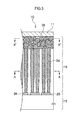
- Fig. 3 is a schematic view schematically showing the construction of a scintillator layer of the radiation image detection apparatus according to an exemplary embodiment of the invention.
- Fig. 6 is a schematic view schematically showing the overall construction of the radiation image detection apparatus.
- the radiation image detection apparatus 10 includes a TFT substrate 16 with switch elements 28 formed on an insulating substrate 12.
- Each of the switch elements 28 is constructed with a Thin-Film Transistor (TFT).
- TFT substrate 16 having a photoelectric transformation layer 26, which will be described later, serves as an optical detector 16.
- the TFT substrate 16 is adhered to a scintillator layer 18, which converts incident radioactive rays into light, via a planarizing layer 23 and an adhesive layer 25 interposed therebetween.
- the scintillator layer 18 is formed on a support 11 as a radiation-converting layer that converts incident radioactive rays (arrows indicate the direction of incidence) into light.
- the scintillator layer 18 can be made of a crystal, for example, of CsI:Tl, Gd 2 O 2 S:Tb (GOS), Thallium-activated Sodium Iodide (NaI:Tl), or Sodium-activated Cesium Iodide (CsI:Na).
- the scintillator layer 18 is not limited to these materials. It is also preferred that the scintillator layer be constructed with CsI:Tl in consideration that emission spectrum matches the maximum value (in the vicinity of 550 nm) of the spectral sensitivity of an a-Si photodiode and that aging deterioration due to humidity rarely occurs.
- a columnar crystal area which includes columnar crystals 34, is present in the radiation incidence side of the scintillator layer 18, and a non-columnar crystals area, which includes non-columnar crystals 36, is present opposite to the radiation incidence side of the scintillator layer.
- the area including the columnar crystals 34 serves to prevent an image from being blurred since the columnar crystals 34, capable of realizing efficient light emission, is present adjacent to the optical detector 16 and the intervals between the columnar crystals 34 function as a guide to reduce light dispersion, thereby preventing the image from being blurred. Furthermore, light, which has reached a deep portion, is reflected from the area constructed with the non-columnar crystals 36, thereby improving the detection efficiency of light emission.
- Fig. 3 is a schematic view showing the crystal area in the scintillator layer 18. Unlike the radiation image detection apparatus shown in Fig. 1 , Fig. 3 shows the state where the optical detector 16 and the scintillator layer 18 are in direct contact with each other without a resin layer, such as the adhesive layer 25, interposed between them.
- t 1 thickness of the area of the columnar crystals 34 present in the radiation incidence side of the scintillator layer 18
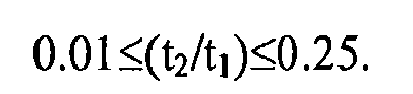
- t 2 it is preferred that the relationship between t 1 and t 2 satisfy the following Formula1. 0.01 ⁇ t 2 / t 1 ⁇ 0.25
- the thickness t 1 of the area of the columnar crystals 34 and the thickness t 2 of the area of the non-columnar crystals 36 satisfy the above Formula1, light emission efficiency, the prevention of light dispersion, and the area, from which light is reflected, in the thickness direction of the scintillator fall within very suitable ranges, thereby further improving light emission efficiency, light detection efficiency, and image resolution. If the thickness t 2 of the non-columnar crystal area is too large, the area with low light emission efficiency increases, thereby leading to a danger of decreased sensitivity. From that point of view, the range of t 2 /t 1 is more preferably from 0.02 to 0.10.
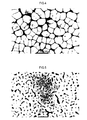
- Fig. 4 is an electron micrograph showing the A-A cross section of the columnar crystals 34 forming the scintillator layer shown in Fig. 3 .
- the columnar crystals 34 have a cross-sectional diameter that is substantially regular with respect to the growth direction of the crystals, and are present independently from each other due to the intervals defined along the circumference of the column portions. It is thought that this area has high light emission efficiency and the intervals between the columnar crystals serve as a light guide that suppresses the spread of light.
- the crystal cross-sectional diameters of the column portions of the columnar crystals are preferably from 2.0 ⁇ m to 15.0 ⁇ m from the viewpoint of efficient light introduction and, more preferably, from 4.0 ⁇ m to 10.0 ⁇ m.
- the crystal cross-sectional diameters indicate the maximum diameters of the crystals observed on the surface in the growth direction of the columnar crystals.
- the column diameter (crystal cross-sectional diameter) is measured by observing the columnar crystals on a surface perpendicular to the film thickness direction of the columnar crystals using a Scanning Electron Microscope (SEM). Observation is performed at a magnification (about 2000 times) that allows 100 to 200 columnar crystals to be observed in one imaging when the scintillator is viewed from the surface, and a value is used that is produced by averaging the maximum column diameters of the columnar crystals for all of the crystals included in one imaging.
- the column diameters ( ⁇ m) are read down to two decimal places, and the average is obtained by rounding off the numbers to one decimal place according to JIS Z 8401.
- Fig. 5 is an electron micrograph showing the cross section of the non-columnar crystals 36 of the scintillator layer 18, taken along line A'-A' in Fig. 3 .
- Fig. 5 shows clearly shown in the non-columnar crystal area, clear intervals between the crystals are rarely observed since the crystals irregularly combine with or overlap each other.
- the crystal cross-sectional diameters of the non-columnar crystals is preferably from 0.5 ⁇ m to 7.0 ⁇ m in the viewpoint of effective reflection, more preferably, from 0.5 ⁇ m to 7.0 ⁇ m, and further more preferably, from 1.0 ⁇ m to 6.0 ⁇ m.
- the crystal shape of the non-columnar crystals be substantially spherical and that the non-columnar crystal area be configured as a combination of crystals, which have a shape similar to a spherical shape (i.e., substantially spherical crystals) from the viewpoint of reflection efficiency.
- the scintillator layer 18, in which the area of the columnar crystals 34 and the area of the non-columnar crystals 36 are formed continuously, can be formed simply over the appropriate support 11 by a vapor deposition method, which will be described below.
- the support 11 can be selected appropriately from the group consisting of a carbon plate, a Carbon Fiber Reinforced Plastic (CFRP), a glass plate, a quartz plate, a sapphire plate, a metal sheet, and the like.
- the metal sheet is made of one selected from the group consisting of iron, tin, chromium, aluminum, and the like.
- the support 11 is not limited particularly to these examples as long as it can form the crystal areas, which form the scintillator layer 18, over the surfaces thereof.
- the insulating substrate 12 can be selected from among, for example, a glass substrate, a variety of ceramic substrates, and a resin substrate. In addition, the insulating substrate 12 is not limited to these materials.
- a bias electrode 22 for applying a bias voltage to the light transmission layer 20 is formed over the surface of each light transmission layer 20, which faces the scintillator layer 18.
- Charge-collecting electrodes 24, which collect electric charges generated by the light transmission layer 20, are formed over the TFT substrate 16.
- the switch elements 28 read the electric charges collected by the individual electric charge-collecting electrodes 24.
- a laminated structure, which includes the respective bias electrode 22, the light transmission layer 20, and the electric charge-collecting electrode 24, is referred to as the photoelectric transformation layer 26.
- the charge-collecting electrodes 24 are arranged in a two-dimensional configuration in the TFT substrate 16 and, as shown in Fig. 2 , the switch elements 28 are arranged on an insulating substrate 12, in a two dimensional configuration corresponding to the charge-collecting electrodes 24.
- gate lines 30 and plural signal lines (data lines) 32 are provided in the TFT substrate 16.
- the gate lines 30 serve to turn on/off the individual switch elements 28 connected in a certain direction (row direction), and the signal lines (data lines) 32 are connected in a certain direction (column direction) perpendicular to the gate lines 30 and serve to read electric charges via the switch elements 28, which are turned on.
- planarizing layer 23 for planarizing the TFT substrate 16 is formed over the TFT substrate 16.
- adhesive layer 25, which bonds the scintillator layer 18 to the TFT substrate 16 is formed between the TFT substrate 16 and the scintillator layer 18 over the planarizing layer 23.
- the adhesive layer 25 and the planarizing layer 23 made of resin are not necessarily required between the TFT substrate 16 and the scintillator layer 18.
- the surface of the TFT substrate 16 can be set to be opposite to and in direct contact with the area of the columnar crystals 34, which forms the scintillator layer 18.
- the TFT substrate 16 has a quadrilateral shape having four sides on the outer circumference when seen in a plan view. Specifically, the TFT substrate 16 is rectangular shaped.
- a connector terminal 38 is arranged on one side of the edges of the TFT substrate 16 when seen in a plan view, and the individual gate lines 30 and the individual signal lines 32 are connected thereto.
- the connector terminal 38 as shown in Fig. 2 , is connected to a circuit substrate via a connecting circuit.
- the circuit substrate includes a gate line driver (not shown) as an outer circuit and a signal processing section (not shown) as an outer circuit.
- the respective switch elements 28 are turned on, sequentially line by line, by signals supplied via the gate lines 30 from the gate line driver. Electric charges read by the turned-on switch elements 28 are transmitted as charge signals via the signal lines 32 and input into the signal processing section. Thereby, the electric charges are read sequentially line by line, so that a two-dimensional radiation image can be acquired.
- the gate lines 30 and the signal lines 32 can be provided in parallel such that the gate lines 30 and the signal lines 32 are connected to the connector terminal arranged on one side of the edges of the TFT substrate 16.
- the radiation image detection apparatus 10 as described above employs indirect conversion mode, which detects radiation by first converting the radiation into light and then converting the light into electric charges.
- the TFT substrate 16 and the scintillator layer 18 are arranged on the surface of the substrate 40 as the optical detector, which was described above. Radiation is allowed to be incident first on the side of the support 40 and then on the scintillator layer 18 through the TFT substrate 16.
- Such a radiation image detection apparatus can be used as being assembled to a variety of apparatuses including an X-ray imaging apparatus for medical use, such as a mammography, which needs a fine image using a small amount of radiation emission capable of detecting a high-sensitivity and high-precision radiation image.
- the range of application of the radiation image detection apparatus is wide since, for example, it can be used as an industrial X-ray imaging apparatus in nondestructive tests or as a detection apparatus that uses particle beams ( ⁇ rays, ⁇ rays, and ⁇ rays) rather than electromagnetic waves.
- the scintillator layer 18 be formed directly over the surface of the support 11 by a vapor deposition method. Due to the vapor deposition method, it is possible to continuously form the non-columnar crystal area and the columnar crystal area in sequence.
- a configuration made of CsI:Tl will be described.
- the vapor deposition method can be performed using a known method. That is, it is preferred that CsI:Tl be evaporated by heating using a means for flowing current through a resistive heating furnace or the like in the atmosphere at a degree of vacuum from 0.01 to 10 Pa, so that CsI:Tl is deposited over the support 11 that has a temperature from room temperature (20 °C) to 300 °C.
- the scintillator layer 18 is formed over the support 11 as above, it is possible to produce the radiation image detection apparatus 10 according to an aspect of the invention by arranging the scintillator layer 18 to overlap an optical detector.
- the method of overlapping the scintillator layer 18 over the optical detector 16 is not specifically limited. Any method can be used as long as both are optically combined.
- a method, which brings both into direct contact by arranging them opposite to each other, or a method, which brings both into contact via any of an adhesive layer or a planarizing layer can be employed.
- the method which brings both elements into direct contact, includes a method of bringing the surface on the side of the scintillator layer 18 at which the columnar crystal area is present and the TFT substrate 16, which serves as the optical detector, into contact with each other by arranging them in opposition to each other after the scintillator layer 18 is formed over the support 11.
- the radiation image detection apparatus 10 is manufactured by stacking and aligning both the scintillator layer 18 and the TFT substrate 16. In the process of bringing the respective elements into contact with each other, it is not required to bring the surfaces of both elements into complete contact with each other.
- the resin layer may include a planarizing layer, which is for planarizing the surface of the scintillator layer 18, an adhesive layer, which fixedly brings both into contact, a matching oil layer, which is made of transparent liquid or gel, and the like.
- the resin, which forms the resin layer is not specifically limited as long as it allows scintillation light, which is generated from the scintillator layer 18, to pass through to the optical detector 16 without reducing the light.
- the resin which forms the planarizing layer
- Polyimide which has good film-forming property, is preferable.
- the adhesive agent which forms the adhesive layer, is not limited to those that are optically transparent to the scintillation light, which is generated from the scintillator layer 18.
- Available examples of the adhesive agent may include a thermoplastic resin, an Ultraviolet (UV) curing adhesive agent, a thermosetting adhesive agent, a room-temperature curing adhesive agent, a double-sided adhesive sheet, and the like. From the viewpoint of not decreasing the sharpness of the image, it is preferred to use an adhesive agent made of a low-viscosity epoxy resin since it can form an adhesive layer that is sufficiently thin in relation to the pixel size of the optical detector 16.
- the thickness of the resin layer is preferably 50 ⁇ m or less from the viewpoints of the sensitivity and image and more preferably in the range from 5 ⁇ m to 30 ⁇ m.
- the manufacturing method according to an aspect of the invention also has an advantage capable of simply and easily manufacturing various specifications of scintillator layers according to designs by controlling the degree of vacuum and the temperature of the support in the forming of the film of the scintillator layer.
- a non-alkali glass substrate (0.7 mm thick) was prepared as a support.
- a support was surface-treated using Ar plasma for the purpose of improving adhesiveness with a CsI crystal layer.
- the surface-treated support was set in a vacuum chamber, which serves to form a scintillator film.
- the vacuum chamber included plural furnaces, which serve to heat raw materials, that is, CsI and T1I independently. After air was exhausted from the chamber, the degree of vacuum was set to be 0.75 Pa by introducing a certain amount of Ar.
- the support was rotated on a concentric circle by an apparatus tool of the vacuum apparatus, a shutter was opened, and deposition of an area of non-columnar crystals 36 was started.
- scintillator layer a scintillator 18, which had the non-columnar crystals 36 and the columnar crystals 34, was formed due to deposition on the support.
- a film thickness was measured by cutting a portion of the scintillator layer and observing the cut portion from the side in the direction of the columnar crystals using a Scanning Electron Microscope (SEM).
- SEM Scanning Electron Microscope
- the value of the film thickness was an average of values measured at 10 random portions, which were selected from the cut portion.
- CsI is nonconductive
- SEM observation was performed after Au was sputtered at about 200 ⁇ .
- a portion of the scintillator layer was peeled off from the support or a light-detecting substrate of Comparative Example 1, which will be described later, and a column diameter (i.e., a cross-sectional diameter of a columnar crystal) was measured by observing the peeled portion in the direction of the film thickness of the columnar crystal using the Scanning Electron Microscope (SEM). Observation was performed at a magnification (about 2000 times) that allows 100 to 200 columnar crystals to be observed by one imaging when the scintillator was viewed from the surface, and the maximum column diameters of the columnar crystals for all of the crystals included in one imaging were measured and averaged.
- SEM Scanning Electron Microscope
- the scintillator layer was sliced in the growth direction of the crystals at a position 100 ⁇ m from the support, was etched using Ar ion up to the distance where phenomena in the surroundings of the grain boundary of the CsI crystals attached to the support could be observed, and was then observed from the etched surface. Since CsI is nonconductive, SEM observation was performed after Au of was sputtered at about 200 ⁇ .
- An optical detector 16 was prepared, and an adhesive layer 25 was formed by applying a low-viscosity epoxy resin adhesive agent (Araldite 2020, trade name, available from Hantman Inc.), diluted with a solvent, on the surface using a spin coater so that the thickness became 15 ⁇ m after the solvent was evaporated.
- the adhesive layer 25 formed over the optical detector 16 and the columnar crystal area of the produced scintillator layer 18 were placed opposite to each other and heated so that the optical detector 16 and the scintillator layer 18 were attached to each other via the adhesive layer 25.
- a TFT-driving circuit substrate and a charge-reading Integrated Circuit (IC) were attached to a terminal of the optical detector 16 via an anisotropic conductive film so as to be connected to a circuit substrate, which serves to perform drive control and Analog-Digital (AD) conversion.
- IC charge-reading Integrated Circuit
- PC Personal Computer
- the optical detector 16 was driven using an electrical circuit when emitting the X-rays, and the amount of electric charges, generated from scintillated light through photoelectric transformation by a photodiode, were calculated by reading the electric charges, amplifying the electric charges using a charge amplifier, and then performing the AD conversion on the electric charges.
- An MTF curve was produced by calculating an edge shape, which was possible to obtain by imaging the MTF edge made of tungsten (W), based on the IEC standard. The result was compared with the value 2 cycle/mm, and was presented as a relative value when the value of Comparative Example 1 was set as 100. The MTF of Example 1 was 100.
- the performance of the radiation image detection apparatus was judged using a product of the evaluation results of the sensitivity and the MTF as an index. It is preferred that the difference in the performance be clearly recognized when the image is subjectively evaluated as the product of the sensitivity and the MTF be 120 or more.
- the comprehensive evaluation of Example 1 was 120, and it can be understood that the sensitivity and the sharpness of the image were better than those of Comparative Example 1, which will be described below.
- a support was changed using the glass substrate used in Example 1, and a glass substrate, on the surface of which recesses and protrusions with pitches of 5 ⁇ m and heights of 5 ⁇ m were formed by wet etching, was used.
- a radiation image detection apparatus of Comparative Example 1 was manufactured in the same fashion as in Example 1, except that deposition on a non-columnar crystal area was not performed in the forming of the scintillator layer but columnar crystals were directly deposited on a support. Evaluation was performed in the same fashion as in Example 1, and relative effects were produced by setting the result of Comparative Example 1 to be 100.
- a support was changed using the glass substrate used in Example 3, and a scintillator layer 18 was formed directly over the surface of the optical detector 16 in the same conditions as in Example 3.
- a non-columnar crystal area was first formed around an optical detector 16, and then a columnar crystal area was formed.
- attachment using a thermoplastic adhesive agent was not performed. Except for this treatment, the process was performed the same as in Example 3.
- Comparative Example 2 having the non-columnar crystal area around the optical detector 16 cannot realize sufficient sensitivity because of scattering and degradation in light emission efficiency in the non-columnar crystal area.
Landscapes
- Physics & Mathematics (AREA)
- Health & Medical Sciences (AREA)
- Life Sciences & Earth Sciences (AREA)
- General Physics & Mathematics (AREA)
- High Energy & Nuclear Physics (AREA)
- Molecular Biology (AREA)
- Spectroscopy & Molecular Physics (AREA)
- Chemical & Material Sciences (AREA)
- Crystallography & Structural Chemistry (AREA)
- Measurement Of Radiation (AREA)
- Apparatus For Radiation Diagnosis (AREA)
- Solid State Image Pick-Up Elements (AREA)
Abstract
Description
- The present invention relates to a radiation image detection apparatus, which is used in an X-ray imaging apparatus for medical use or the like, and a manufacturing method of the same.
- In recent years, a radiation image detection apparatus, such as a Flat Panel Detector (FPD), capable of directly converting radiation into digital data, has been put to practical use. The radiation image detection apparatus is being rapidly distributed since it has an advantage of being able to immediately verify an image compared to conventional image plates.
- Various types of such radiation image detection apparatuses were proposed. For example, an indirect type converts radiation into light in a single operation using a scintillator of, for example, CsI:Tl, GOS (Gd2O2S:Tb) , or the like, converts the converted light into electric charges through a semiconductor layer, and then stores the electric charges.
- It is preferred to decrease the amount of radiation emitted when the radiation image detection apparatus is used, for example, in living bodies. In the field of optical detectors, the scintillator, which emits a great amount of light and has high sensitivity, is preferable. From that point of view, several radiation image detection apparatuses were proposed (e.g., Japanese Patent No.
3333278 2001-330677 - In the scintillator, which is configured to include such crystals, it is known in theory that sensitivity rises as according to the thickness of the crystals. In practice, however, if the thickness of the crystals is increased up to a certain value, light is attenuated or scattered while it is passing through the scintillator. This causes problems such as being unable to obtain sufficient sensitivity or blurring of an image. Therefore, additional improvement in sensitivity is required.
- For the purpose of improving sensitivity, a radiation image detection apparatus was proposed, in which a scintillator layer is constructed with an assembly of columnar crystals, and which ensures that the density of an activator has a slope (e.g.,
JP-A No. 2008-51793 - The present invention has been made in view of the above circumstances and provides a radiation image detection apparatus, which has excellent detection sensitivity and prevents the sharpness of a radiation image from decreasing, and a simple manufacturing method of the same.
-
- (1) A radiation image detection apparatus comprising a scintillator, which is configured to include columnar crystals and converts radiation into light when the radiation is irradiated thereon, and an optical detector, which converts the light emitted from the scintillator into an electrical signal, the scintillator and the optical detector being arranged on a support such that the radiation is incident on the optical detector and the scintillator in this order,
wherein a columnar crystal area is present at a radiation-incident side of the scintillator, and a non-columnar crystal area is present at a side of the scintillator opposite to the radiation-incident side.
According to (1), since the columnar crystal area having high light emission efficiency is present in the radiation incidence side of the scintillator, it is possible to produce efficient light emission in the surroundings of the optical detector. In addition, in order to accomplish the function as a light guide, intervals between the columnar crystals allow emitted light to efficiently pass through, thereby preventing the image from being blurred. Furthermore, in order to accomplish the function as a reflecting layer, the non-columnar crystal area in the deep portion of the scintillator efficiently reflects light, which has propagated in the direction opposite to the optical direction, from the deep portion of the scintillator, thereby improving the detection efficiency of light emission. Accordingly, an image, which has good sensitivity and high sharpness, is detected. - (2) The radiation image detection apparatus according to (1), wherein a thickness t1 of the columnar crystal area at the radiation-incident side of the scintillator and a thickness t2 of the non-columnar crystal area at the side opposite to the radiation-incident side of the scintillator have a relationship that satisfies the following Formula 1:

Since the thickness of the columnar crystal area and the thickness of the non-columnar crystal area satisfy the above Formula1, light emission as well as the guidance and reflection of light in the thickness direction of the scintillator are carried out in a preferable area and the sensitivity of light detection and the resolution of the image are further improved. - (3) The radiation image detection apparatus according to (2), wherein the thickness t1 of the columnar crystal area and the thickness t2 of the non-columnar crystal area have a relationship that satisfies the following Formula 2:

- (4) The radiation image detection apparatus according to any one of (1) to (3), wherein non-columnar crystals in the non-columnar crystal area have a cross-sectional diameter from 0.5 µm to 7.0 µm.
- (5) The radiation image detection apparatus according to any one of (1) to (4), wherein the columnar crystals in the columnar crystal area have a cross-sectional diameter from 2.0 µm to 15.0 µm.
- (6) The radiation image detection apparatus according to any one of (1) to (5), wherein the scintillator is configured to include crystals that contain CsI and Tl.
- (7) The radiation image detection apparatus according to any one of (1) to (6), wherein the scintillator is formed on the support by a vapor deposition method.
- (8) The radiation image detection apparatus according to any one of (1) to (7), wherein a surface of the side of the scintillator at which the columnar crystal area is present and the optical detector are arranged so as to oppose each other and are optically combined via a resin layer.
- (9) The radiation image detection apparatus according to (8), wherein the resin layer comprises at least one selected from the group consisting of a planarizing layer, an adhesive layer, and a matching oil layer.
- (10) The radiation image detection apparatus according to (9), wherein the planarizing layer comprises polyimide or parylene.
- (11) The radiation image detection apparatus according to (9), wherein the adhesive layer comprises an adhesive agent comprising a low-viscosity epoxy resin.
- (12) A method of manufacturing a radiation image detection apparatus according to any one of (1) to (11), comprising forming a scintillator on a support by a vapor deposition method, so as to form a non-columnar crystal area and a columnar crystal area in this order on the support by changing one or both conditions of a degree of vacuum and a temperature of the support.
Through this process, the non-columnar crystal area and the columnar crystal area of the scintillator are easily formed in sequence. In addition, it is possible to control the shape or thickness of each crystal area to be an intended size by controlling individual conditions of the degree of vacuum and the temperature of the support and the timing to change the conditions. - (13) The method according to (12), further comprising, after forming the scintillator, bringing a surface of a side of the scintillator at which the columnar crystal area is present into opposition to and close contact with the optical detector.
- (14) The method according to (12), further comprising, after forming the scintillator, optically combining a surface of a side of the scintillator at which the columnar crystal area is present with the optical detector by arranging the surface of the side of the scintillator and the optical detector in opposition to each other via a resin layer.
Since the present invention has the above-described configurations (13) and (14), it can advantageously provide the radiation image detection apparatus, which has excellent light detection sensitivity and prevents the sharpness of a radiation image from decreasing, and the simple manufacturing method of the same. -
-
Fig. 1 is a schematic side view schematically showing the construction of a radiation image detection apparatus related to indirect conversion mode. -
Fig. 2 is a schematic view schematically showing the construction of a radiation detection apparatus according to an exemplary embodiment of the invention. -
Fig. 3 is a schematic view schematically showing the crystal construction of a scintillator section of the radiation image detection apparatus according to an exemplary embodiment of the invention. -
Fig. 4 is an electron micrograph showing a columnar crystal area that forms a scintillator. -
Fig. 5 is an electron micrograph showing a non-columnar crystal cross section of a non-columnar crystal area that forms a scintillator. -
Fig. 6 is a schematic view schematically showing the overall construction of the radiation image detection apparatus according to an exemplary embodiment of the invention. - Hereinafter, radiation image detection apparatuses according to exemplary embodiments of the invention will now be described with reference to the accompanying drawings.
- A radiation image detection apparatus according to an exemplary embodiment of the invention is used in an X-ray imaging apparatus or the like. The radiation image detection apparatus includes a light-emitting layer, which emits light when radiation is irradiated thereon, and a conductive layer, which converts the light of the light-emitting layer. When the radiation, which contains image information, is irradiated on the radiation image detection apparatus, it records the image information and outputs an image signal, which represents the recorded image information.
- Below, a description will be given of an exemplary embodiment of the invention with reference to the drawings.
- First, the construction of a radiation image detection apparatus according to an exemplary embodiment of the invention will be described.
Fig. 1 is a schematic side view schematically showing the construction of a radiation image detection apparatus related to indirect conversion mode.Fig. 2 is a schematic view schematically showing the construction of a radiation image detection apparatus according to an exemplary embodiment of the invention, viewed from the support side.Fig. 3 is a schematic view schematically showing the construction of a scintillator layer of the radiation image detection apparatus according to an exemplary embodiment of the invention.Fig. 6 is a schematic view schematically showing the overall construction of the radiation image detection apparatus. - As shown in
Fig. 1 , the radiationimage detection apparatus 10 includes aTFT substrate 16 withswitch elements 28 formed on aninsulating substrate 12. Each of theswitch elements 28 is constructed with a Thin-Film Transistor (TFT). In this embodiment, theTFT substrate 16 having aphotoelectric transformation layer 26, which will be described later, serves as anoptical detector 16. - The
TFT substrate 16 is adhered to ascintillator layer 18, which converts incident radioactive rays into light, via aplanarizing layer 23 and anadhesive layer 25 interposed therebetween. Thescintillator layer 18 is formed on asupport 11 as a radiation-converting layer that converts incident radioactive rays (arrows indicate the direction of incidence) into light. - The
scintillator layer 18 can be made of a crystal, for example, of CsI:Tl, Gd2O2S:Tb (GOS), Thallium-activated Sodium Iodide (NaI:Tl), or Sodium-activated Cesium Iodide (CsI:Na). However, thescintillator layer 18 is not limited to these materials. It is also preferred that the scintillator layer be constructed with CsI:Tl in consideration that emission spectrum matches the maximum value (in the vicinity of 550 nm) of the spectral sensitivity of an a-Si photodiode and that aging deterioration due to humidity rarely occurs. - Below, a detailed description will be given of the
scintillator layer 18 of this exemplary embodiment. - In this exemplary embodiment, a columnar crystal area, which includes
columnar crystals 34, is present in the radiation incidence side of thescintillator layer 18, and a non-columnar crystals area, which includesnon-columnar crystals 36, is present opposite to the radiation incidence side of the scintillator layer. - The area including the
columnar crystals 34 serves to prevent an image from being blurred since thecolumnar crystals 34, capable of realizing efficient light emission, is present adjacent to theoptical detector 16 and the intervals between thecolumnar crystals 34 function as a guide to reduce light dispersion, thereby preventing the image from being blurred. Furthermore, light, which has reached a deep portion, is reflected from the area constructed with thenon-columnar crystals 36, thereby improving the detection efficiency of light emission. -
Fig. 3 is a schematic view showing the crystal area in thescintillator layer 18. Unlike the radiation image detection apparatus shown inFig. 1 ,Fig. 3 shows the state where theoptical detector 16 and thescintillator layer 18 are in direct contact with each other without a resin layer, such as theadhesive layer 25, interposed between them. As shown inFig. 3 , when the thickness of the area of thecolumnar crystals 34 present in the radiation incidence side of thescintillator layer 18 is set to be t1, and the thickness of the area of thenon-colunmar crystals 36 present opposite to the radiation incidence side of thescintillator layer 18 is set to be t2, it is preferred that the relationship between t1 and t2 satisfy the following Formula1.
- Since the thickness t1 of the area of the
columnar crystals 34 and the thickness t2 of the area of thenon-columnar crystals 36 satisfy the above Formula1, light emission efficiency, the prevention of light dispersion, and the area, from which light is reflected, in the thickness direction of the scintillator fall within very suitable ranges, thereby further improving light emission efficiency, light detection efficiency, and image resolution. If the thickness t2 of the non-columnar crystal area is too large, the area with low light emission efficiency increases, thereby leading to a danger of decreased sensitivity. From that point of view, the range of t2/t1 is more preferably from 0.02 to 0.10. -
Fig. 4 is an electron micrograph showing the A-A cross section of thecolumnar crystals 34 forming the scintillator layer shown inFig. 3 . As clearly shown inFig. 4 , it can be appreciated that, in the area including thecolumnar crystals 34, thecolumnar crystals 34 have a cross-sectional diameter that is substantially regular with respect to the growth direction of the crystals, and are present independently from each other due to the intervals defined along the circumference of the column portions. It is thought that this area has high light emission efficiency and the intervals between the columnar crystals serve as a light guide that suppresses the spread of light. - Here, the crystal cross-sectional diameters of the column portions of the columnar crystals are preferably from 2.0 µm to 15.0 µm from the viewpoint of efficient light introduction and, more preferably, from 4.0 µm to 10.0 µm.
- In addition, according to an aspect of the invention, the crystal cross-sectional diameters indicate the maximum diameters of the crystals observed on the surface in the growth direction of the columnar crystals. In a detailed measuring method, the column diameter (crystal cross-sectional diameter) is measured by observing the columnar crystals on a surface perpendicular to the film thickness direction of the columnar crystals using a Scanning Electron Microscope (SEM). Observation is performed at a magnification (about 2000 times) that allows 100 to 200 columnar crystals to be observed in one imaging when the scintillator is viewed from the surface, and a value is used that is produced by averaging the maximum column diameters of the columnar crystals for all of the crystals included in one imaging. The column diameters (µm) are read down to two decimal places, and the average is obtained by rounding off the numbers to one decimal place according to JIS Z 8401.
-
Fig. 5 is an electron micrograph showing the cross section of thenon-columnar crystals 36 of thescintillator layer 18, taken along line A'-A' inFig. 3 . As clearly shown inFig. 5 , in the non-columnar crystal area, clear intervals between the crystals are rarely observed since the crystals irregularly combine with or overlap each other. - If crystals are adhered to each other as in the non-columnar crystal area, it is thought that a line that binds vacancies (depressions) between adjacent crystals is a grain boundary, and column diameters and crystal cross-sectional diameters corresponding to the column diameters are measured by dividing the adhered crystals from each other so that they become minimum polygons. The crystal diameters are averaged in the same fashion as in the columnar crystal area, and the average is used.
- The crystal cross-sectional diameters of the non-columnar crystals is preferably from 0.5 µm to 7.0 µm in the viewpoint of effective reflection, more preferably, from 0.5 µm to 7.0 µm, and further more preferably, from 1.0 µm to 6.0 µm.
- In addition, it is preferred that the crystal shape of the non-columnar crystals be substantially spherical and that the non-columnar crystal area be configured as a combination of crystals, which have a shape similar to a spherical shape (i.e., substantially spherical crystals) from the viewpoint of reflection efficiency.
- The
scintillator layer 18, in which the area of thecolumnar crystals 34 and the area of thenon-columnar crystals 36 are formed continuously, can be formed simply over theappropriate support 11 by a vapor deposition method, which will be described below. - The
support 11 can be selected appropriately from the group consisting of a carbon plate, a Carbon Fiber Reinforced Plastic (CFRP), a glass plate, a quartz plate, a sapphire plate, a metal sheet, and the like. The metal sheet is made of one selected from the group consisting of iron, tin, chromium, aluminum, and the like. However, thesupport 11 is not limited particularly to these examples as long as it can form the crystal areas, which form thescintillator layer 18, over the surfaces thereof. - The insulating
substrate 12 can be selected from among, for example, a glass substrate, a variety of ceramic substrates, and a resin substrate. In addition, the insulatingsubstrate 12 is not limited to these materials. - Light transmission layers 20, which generate electric charges when light converted by the
scintillator layer 18 is incident, are arranged between thescintillator layer 18 and theTFT substrate 16. Abias electrode 22 for applying a bias voltage to thelight transmission layer 20 is formed over the surface of eachlight transmission layer 20, which faces thescintillator layer 18. - Charge-collecting
electrodes 24, which collect electric charges generated by thelight transmission layer 20, are formed over theTFT substrate 16. In theTFT substrate 16, theswitch elements 28 read the electric charges collected by the individual electric charge-collectingelectrodes 24. A laminated structure, which includes therespective bias electrode 22, thelight transmission layer 20, and the electric charge-collectingelectrode 24, is referred to as thephotoelectric transformation layer 26. - The charge-collecting
electrodes 24 are arranged in a two-dimensional configuration in theTFT substrate 16 and, as shown inFig. 2 , theswitch elements 28 are arranged on an insulatingsubstrate 12, in a two dimensional configuration corresponding to the charge-collectingelectrodes 24. - In addition,
plural gate lines 30 and plural signal lines (data lines) 32 are provided in theTFT substrate 16. The gate lines 30 serve to turn on/off theindividual switch elements 28 connected in a certain direction (row direction), and the signal lines (data lines) 32 are connected in a certain direction (column direction) perpendicular to the gate lines 30 and serve to read electric charges via theswitch elements 28, which are turned on. - In addition, the
planarizing layer 23 for planarizing theTFT substrate 16 is formed over theTFT substrate 16. In addition, theadhesive layer 25, which bonds thescintillator layer 18 to theTFT substrate 16, is formed between theTFT substrate 16 and thescintillator layer 18 over theplanarizing layer 23. - In addition, as described below, the
adhesive layer 25 and theplanarizing layer 23 made of resin are not necessarily required between theTFT substrate 16 and thescintillator layer 18. The surface of theTFT substrate 16 can be set to be opposite to and in direct contact with the area of thecolumnar crystals 34, which forms thescintillator layer 18. - The
TFT substrate 16 has a quadrilateral shape having four sides on the outer circumference when seen in a plan view. Specifically, theTFT substrate 16 is rectangular shaped. - A
connector terminal 38 is arranged on one side of the edges of theTFT substrate 16 when seen in a plan view, and theindividual gate lines 30 and theindividual signal lines 32 are connected thereto. Theconnector terminal 38, as shown inFig. 2 , is connected to a circuit substrate via a connecting circuit. The circuit substrate includes a gate line driver (not shown) as an outer circuit and a signal processing section (not shown) as an outer circuit. - The
respective switch elements 28 are turned on, sequentially line by line, by signals supplied via the gate lines 30 from the gate line driver. Electric charges read by the turned-onswitch elements 28 are transmitted as charge signals via thesignal lines 32 and input into the signal processing section. Thereby, the electric charges are read sequentially line by line, so that a two-dimensional radiation image can be acquired. - In addition, while the
signal lines 32 and the gate lines 30 are provided so as to bisect each other at right angles in the configuration described above, the gate lines 30 and thesignal lines 32 can be provided in parallel such that the gate lines 30 and thesignal lines 32 are connected to the connector terminal arranged on one side of the edges of theTFT substrate 16. - The radiation
image detection apparatus 10 as described above employs indirect conversion mode, which detects radiation by first converting the radiation into light and then converting the light into electric charges. - In this exemplary embodiment, as shown in
Fig. 6 , theTFT substrate 16 and thescintillator layer 18 are arranged on the surface of thesubstrate 40 as the optical detector, which was described above. Radiation is allowed to be incident first on the side of thesupport 40 and then on thescintillator layer 18 through theTFT substrate 16. - Such a radiation image detection apparatus can be used as being assembled to a variety of apparatuses including an X-ray imaging apparatus for medical use, such as a mammography, which needs a fine image using a small amount of radiation emission capable of detecting a high-sensitivity and high-precision radiation image. The range of application of the radiation image detection apparatus is wide since, for example, it can be used as an industrial X-ray imaging apparatus in nondestructive tests or as a detection apparatus that uses particle beams (α rays, β rays, and γ rays) rather than electromagnetic waves.
- Next, a description will be given of a method of manufacturing a radiation image detection apparatus, the method capable of efficiently manufacturing the radiation image detection apparatus of the invention as described above.
- It is preferred that the
scintillator layer 18 be formed directly over the surface of thesupport 11 by a vapor deposition method. Due to the vapor deposition method, it is possible to continuously form the non-columnar crystal area and the columnar crystal area in sequence. Here, by way of example, a configuration made of CsI:Tl will be described. - The vapor deposition method can be performed using a known method. That is, it is preferred that CsI:Tl be evaporated by heating using a means for flowing current through a resistive heating furnace or the like in the atmosphere at a degree of vacuum from 0.01 to 10 Pa, so that CsI:Tl is deposited over the
support 11 that has a temperature from room temperature (20 °C) to 300 °C. - When forming a crystal phase of CsI:Tl over the
support 11 by the vapor deposition method, it is usual that a cluster of relatively small crystals, which has a diameter corresponding to that of an indeterminate or substantially spherical crystal, is formed. When the vapor deposition method is carried out, it is possible to grow the columnar crystals by the vapor deposition method, continuously after the non-columnar crystal area is formed, by changing the condition of the degree of vacuum and/or the temperature of the support. - That is, after the non-columnar crystal area is formed up to a certain thickness t2, it is possible to efficiently and uniformly grow columnar crystals using at least one of a means for raising the degree of vacuum and a means for raising the temperature of the support.
- After the
scintillator layer 18 is formed over thesupport 11 as above, it is possible to produce the radiationimage detection apparatus 10 according to an aspect of the invention by arranging thescintillator layer 18 to overlap an optical detector. The method of overlapping thescintillator layer 18 over theoptical detector 16 is not specifically limited. Any method can be used as long as both are optically combined. As the method of arranging both to overlap, a method, which brings both into direct contact by arranging them opposite to each other, or a method, which brings both into contact via any of an adhesive layer or a planarizing layer, can be employed. - The method, which brings both elements into direct contact, includes a method of bringing the surface on the side of the
scintillator layer 18 at which the columnar crystal area is present and theTFT substrate 16, which serves as the optical detector, into contact with each other by arranging them in opposition to each other after thescintillator layer 18 is formed over thesupport 11. In this fashion, the radiationimage detection apparatus 10 is manufactured by stacking and aligning both thescintillator layer 18 and theTFT substrate 16. In the process of bringing the respective elements into contact with each other, it is not required to bring the surfaces of both elements into complete contact with each other. Even if depressions and protrusions formed by the crystals are present on the surface of thescintillator layer 18, both can be optically combined with each other by being arranged one over the other. When light converted from radiation by thescintillator layer 18 is incident on theTFT substrate 16, the effects of the invention can be obtained. - In addition, it is preferred to optically combine both by bringing the surface of the side of the formed
scintillator layer 18, in which the area ofcolumnar crystals 34 is present, and theoptical detector 16 to be opposite to each other via a resin layer. Available examples of the resin layer may include a planarizing layer, which is for planarizing the surface of thescintillator layer 18, an adhesive layer, which fixedly brings both into contact, a matching oil layer, which is made of transparent liquid or gel, and the like. The resin, which forms the resin layer, is not specifically limited as long as it allows scintillation light, which is generated from thescintillator layer 18, to pass through to theoptical detector 16 without reducing the light. - Available examples of the resin, which forms the planarizing layer, may include polyimide, parylene, and the like. Polyimide, which has good film-forming property, is preferable.
- The adhesive agent, which forms the adhesive layer, is not limited to those that are optically transparent to the scintillation light, which is generated from the
scintillator layer 18. Available examples of the adhesive agent may include a thermoplastic resin, an Ultraviolet (UV) curing adhesive agent, a thermosetting adhesive agent, a room-temperature curing adhesive agent, a double-sided adhesive sheet, and the like. From the viewpoint of not decreasing the sharpness of the image, it is preferred to use an adhesive agent made of a low-viscosity epoxy resin since it can form an adhesive layer that is sufficiently thin in relation to the pixel size of theoptical detector 16. - In addition, as described above, the thickness of the resin layer is preferably 50 µm or less from the viewpoints of the sensitivity and image and more preferably in the range from 5 µm to 30 µm.
- According to the method as described above, it is possible to efficiently and easily manufacture the radiation image detection apparatus according to an aspect of the invention. In addition, the manufacturing method according to an aspect of the invention also has an advantage capable of simply and easily manufacturing various specifications of scintillator layers according to designs by controlling the degree of vacuum and the temperature of the support in the forming of the film of the scintillator layer.
- Below, the present invention will be described in detail with respect to Examples. However, the present invention is not limited to the detailed Examples.
- A non-alkali glass substrate (0.7 mm thick) was prepared as a support.
- First, a support was surface-treated using Ar plasma for the purpose of improving adhesiveness with a CsI crystal layer. Afterwards, the surface-treated support was set in a vacuum chamber, which serves to form a scintillator film. The vacuum chamber included plural furnaces, which serve to heat raw materials, that is, CsI and T1I independently. After air was exhausted from the chamber, the degree of vacuum was set to be 0.75 Pa by introducing a certain amount of Ar. At a time point when the melting conditions of the raw materials were stabilized due to heating of the raw material furnaces, the support was rotated on a concentric circle by an apparatus tool of the vacuum apparatus, a shutter was opened, and deposition of an area of
non-columnar crystals 36 was started. - Film-forming was carried out under these conditions, and at a time point when the thickness t2 of the
non-columnar crystals 36 became 5 µm, deposition ofcolumnar crystals 34 was started by raising the degree of vacuum to 1 Pa. In addition, in the case of changing the degree of vacuum, in order to change the melting conditions of the raw materials, it was confirmed whether or not the melting conditions were stabilized by closing the shutter in one operation and the deposition was then started again by opening the shutter in the next operation. At a time point when the thickness t1 of thecolumnar crystals 34 became 500 µm, heating of the raw material furnaces was stopped and suction using was performed a vacuum apparatus so that a scintillator (hereinafter, referred to as scintillator layer) 18, which had thenon-columnar crystals 36 and thecolumnar crystals 34, was formed due to deposition on the support. - A film thickness was measured by cutting a portion of the scintillator layer and observing the cut portion from the side in the direction of the columnar crystals using a Scanning Electron Microscope (SEM). The value of the film thickness was an average of values measured at 10 random portions, which were selected from the cut portion. In addition, since CsI is nonconductive, SEM observation was performed after Au was sputtered at about 200 Å.
- A portion of the scintillator layer was peeled off from the support or a light-detecting substrate of Comparative Example 1, which will be described later, and a column diameter (i.e., a cross-sectional diameter of a columnar crystal) was measured by observing the peeled portion in the direction of the film thickness of the columnar crystal using the Scanning Electron Microscope (SEM). Observation was performed at a magnification (about 2000 times) that allows 100 to 200 columnar crystals to be observed by one imaging when the scintillator was viewed from the surface, and the maximum column diameters of the columnar crystals for all of the crystals included in one imaging were measured and averaged.
- In addition, if crystals are adhered to each other as in the non-columnar crystal area, it was regarded that a line, which binds depressions (recesses) between adjacent crystals, was a grain boundary, and column diameters and crystal diameters corresponding to the column diameters were measured by dividing the adhered crystals from each other so that they became minimum polygons. The column diameters (µm) were read down to two decimal places, and an average was obtained by rounding off the numbers to one decimal place according to JIS Z 8401.
- If it was difficult to peel the scintillator layer from the support, the scintillator layer was sliced in the growth direction of the crystals at a position 100 µm from the support, was etched using Ar ion up to the distance where phenomena in the surroundings of the grain boundary of the CsI crystals attached to the support could be observed, and was then observed from the etched surface. Since CsI is nonconductive, SEM observation was performed after Au of was sputtered at about 200 Å.
- An
optical detector 16 was prepared, and anadhesive layer 25 was formed by applying a low-viscosity epoxy resin adhesive agent (Araldite 2020, trade name, available from Hantman Inc.), diluted with a solvent, on the surface using a spin coater so that the thickness became 15 µm after the solvent was evaporated. Theadhesive layer 25 formed over theoptical detector 16 and the columnar crystal area of the producedscintillator layer 18 were placed opposite to each other and heated so that theoptical detector 16 and thescintillator layer 18 were attached to each other via theadhesive layer 25. - Afterwards, a TFT-driving circuit substrate and a charge-reading Integrated Circuit (IC) were attached to a terminal of the
optical detector 16 via an anisotropic conductive film so as to be connected to a circuit substrate, which serves to perform drive control and Analog-Digital (AD) conversion. Thereby, a radiationimage detection apparatus 10 of Example 1 was manufactured. - It was arranged so that radiation is incident from the
optical detector 16 side, and reading of a radiation image was performed by controlling a scanning Personal Computer (PC), which was connected to the radiationimage detection apparatus 10 via a cable. - X-rays were used for radiation. The
optical detector 16 was driven using an electrical circuit when emitting the X-rays, and the amount of electric charges, generated from scintillated light through photoelectric transformation by a photodiode, were calculated by reading the electric charges, amplifying the electric charges using a charge amplifier, and then performing the AD conversion on the electric charges. - An amount of electric charges (noises of the detection apparatus), which was read when X-rays were not being emitted, was measured in advance and was subtracted from an amount of electric charges, which was read when X-rays were being emitted, and the subtracted value was set as the sensitivity. In addition, the result is presented as a relative value when sensitivity in Comparative Example 1 was set as 100, which will be described later. The sensitivity in Example 1 was 120.
- An MTF curve was produced by calculating an edge shape, which was possible to obtain by imaging the MTF edge made of tungsten (W), based on the IEC standard. The result was compared with the value 2 cycle/mm, and was presented as a relative value when the value of Comparative Example 1 was set as 100. The MTF of Example 1 was 100.
- The performance of the radiation image detection apparatus was judged using a product of the evaluation results of the sensitivity and the MTF as an index. It is preferred that the difference in the performance be clearly recognized when the image is subjectively evaluated as the product of the sensitivity and the MTF be 120 or more. The comprehensive evaluation of Example 1 was 120, and it can be understood that the sensitivity and the sharpness of the image were better than those of Comparative Example 1, which will be described below.
- A support was changed using the glass substrate used in Example 1, and a glass substrate, on the surface of which recesses and protrusions with pitches of 5 µm and heights of 5 µm were formed by wet etching, was used.
- A radiation image detection apparatus of Comparative Example 1 was manufactured in the same fashion as in Example 1, except that deposition on a non-columnar crystal area was not performed in the forming of the scintillator layer but columnar crystals were directly deposited on a support. Evaluation was performed in the same fashion as in Example 1, and relative effects were produced by setting the result of Comparative Example 1 to be 100.
- Radiation image detection apparatuses of Examples 2 to 6 were manufactured in the same fashion as in Example 1, except for setting the thickness of the non-columnar crystal area in Example 1 according to the description in Table 1 by changing the deposition time when the degree of vacuum was 0.75 Pa, and were evaluated in the same fashion. The results are presented in Table 1 below.
- Radiation image detection apparatuses of Examples 7 to 11 were manufactured in the same fashion as in Example 1, except for forming the film of the non-columnar crystal area in Example 1 by changing the degree of vacuum according to the description in Table 1 so that the crystal diameters in the non-columnar crystal area were the same as the description in Table 1, and were evaluated in the same fashion. The results are reported in Table 1 below.
- A support was changed using the glass substrate used in Example 3, and a
scintillator layer 18 was formed directly over the surface of theoptical detector 16 in the same conditions as in Example 3. In this state, a non-columnar crystal area was first formed around anoptical detector 16, and then a columnar crystal area was formed. Thus, attachment using a thermoplastic adhesive agent was not performed. Except for this treatment, the process was performed the same as in Example 3.[Table 1] Method of forming scintillator film Morphology of scintillator Evaluation result Support Degree of vacuum Non-columnar crystal area Columnar crystal area Film thickness ratio t2/t1 Sensitivity MTF Comprehensive evaluation Non-columnar crystal area Columnar crystal area Film thickness t2 (µm) Average crystal diameter (µm) Film thickness t1 (µm) Average column diameter (µm) Ex.1 Non-alkali glass 0.75 Pa 1Pa 5 3.3 500 7.6 0.01 120 100 120 Ex.2 Non-alkali glass 0.75 Pa 1Pa 10 3.0 500 7. 2 0.02 121 100 121 Ex.3 Non-alkali glass 0.75 Pa 1Pa 25 3.0 500 6.8 0.05 123 101 124 Ex.4 Non-alkali glass 0.75 Pa 1Pa 50 3.1 500 7.2 0.10 122 100 122 Ex.5 Non-alkali glass 0.75 Pa 1Pa 125 3.4 500 7.1 0.25 120 100 120 Ex.6 Non-alkali glass 0.75 Pa 1Pa 170 3.2 500 7.0 0.34 121 94 114 Ex.7 Non-alkali glass 0.1 Pa 1Pa 25 11.2 500 6.8 0.05 111 91 101 Ex.8 Non-alkali glass 0.3 Pa 1Pa 25 8.0 500 7.0 0.05 117 99 116 Ex.9 Non-alkali glass 0.5 Pa 1Pa 25 6.2 500 7.0 0.05 123 100 123 Vex.10 Non-alkali glass 1.5 Pa 1Pa 25 1.5 500 7.2 0.05 122 100 122 Ex.11 Non-alkali glass 3 Pa 1Pa 25 0.5 500 7.0 0.05 122 100 122 Comp. Ex. 1 Patterning substrate - 1Pa - - 530 6.8 - 100 100 100 Comp. Ex. 2 Optical detector (TFT) substrate 0.75 Pa 1Pa 25 3.1 500 6.9 0.05 98 96 94 - As apparent from Table 1, it can be understood that images produced from the radiation image detection apparatuses of Examples 1 to 11 of the invention have high sensitivity and higher sharpness than those produced from Comparative Example 1, in which the scintillator layer was made entirely of the columnar crystals, since degradation in image quality, such as image blurring, was prevented.
- Meanwhile, it can be understood that Comparative Example 2 having the non-columnar crystal area around the
optical detector 16 cannot realize sufficient sensitivity because of scattering and degradation in light emission efficiency in the non-columnar crystal area. - In addition, it can be understood from Examples 1 to 11, in particular, that sensitivity is good and image blurring is prevented if the ratio t2/t1 between the thickness t1 of the columnar crystal area and the thickness t2 of the non-columnar crystal area is in a preferred range and the crystal diameter of the non-columnar crystals is in a preferred range.
- All publications, patent applications, and technical standards mentioned in this specification are herein incorporated by reference to the same extent as if each individual publication, patent application, or technical standard was specifically and individually indicated to be incorporated by reference.
Claims (14)
- A radiation image detection apparatus comprising a scintillator, which is configured to include columnar crystals and converts radiation into light when the radiation is irradiated thereon, and an optical detector, which converts the light emitted from the scintillator into an electrical signal, the scintillator and the optical detector being arranged on a support such that the radiation is incident on the optical detector and the scintillator in this order,
wherein a columnar crystal area is present at a radiation-incident side of the scintillator, and a non-colunnar crystal area is present at a side of the scintillator opposite to the radiation-incident side. - The radiation image detection apparatus according to claim 1, wherein a thickness t1 of the columnar crystal area at the radiation-incident side of the scintillator and a thickness t2 of the non-columnar crystal area at the side opposite to the radiation-incident side of the scintillator have a relationship that satisfies the following Formula 1:
- The radiation image detection apparatus according to claim 2, wherein the thickness t1 of the columnar crystal area and the thickness t2 of the non-columnar crystal area have a relationship that satisfies the following Formula 2:

- The radiation image detection apparatus according to any one of claims 1 to 3, wherein non-columnar crystals in the non-columnar crystal area have a cross-sectional diameter from 0.5 µm to 7.0 µm.
- The radiation image detection apparatus according to any one of claims 1 to 4, wherein the columnar crystals in the columnar crystal area have a cross-sectional diameter from 2.0 µm to 15.0 µm.
- The radiation image detection apparatus according to any one of claims 1 to 5, wherein the scintillator is configured to include crystals that contain CsI and T1.
- The radiation image detection apparatus according to any one of claims 1 to 6, wherein the scintillator is formed on the support by a vapor deposition method.
- The radiation image detection apparatus according to any one of claims 1 to 7, wherein a surface of the side of the scintillator at which the columnar crystal area is present and the optical detector are arranged so as to oppose each other and are optically combined via a resin layer.
- The radiation image detection apparatus according to claim 8, wherein the resin layer comprises at least one selected from the group consisting of a planarizing layer, an adhesive layer, and a matching oil layer.
- The radiation image detection apparatus according to claim 9, wherein the planarizing layer comprises polyimide or parylene.
- The radiation image detection apparatus according to claim 9, wherein the adhesive layer comprises an adhesive agent comprising a low-viscosity epoxy resin.
- A method of manufacturing a radiation image detection apparatus according to any one of claims 1 to 11, comprising forming a scintillator on a support by a vapor deposition method, so as to form a non-columnar crystal area and a columnar crystal area in this order on the support by changing one or both conditions of a degree of vacuum and a temperature of the support.
- The method according to claim 12, further comprising, after forming the scintillator, bringing a surface of a side of the scintillator at which the columnar crystal area is present into opposition to and close contact with the optical detector.
- The method according to claim 12, further comprising, after forming the scintillator, optically combining a surface of a side of the scintillator at which the columnar crystal area is present with the optical detector by arranging the surface of the side of the scintillator and the optical detector in opposition to each other via a resin layer.
Applications Claiming Priority (1)
| Application Number | Priority Date | Filing Date | Title |
|---|---|---|---|
| JP2009164205A JP2011017683A (en) | 2009-07-10 | 2009-07-10 | Radiation image detector, and manufacturing method of the same |
Publications (2)
| Publication Number | Publication Date |
|---|---|
| EP2273286A2 true EP2273286A2 (en) | 2011-01-12 |
| EP2273286A3 EP2273286A3 (en) | 2011-04-20 |
Family
ID=42989321
Family Applications (1)
| Application Number | Title | Priority Date | Filing Date |
|---|---|---|---|
| EP10168292A Ceased EP2273286A3 (en) | 2009-07-10 | 2010-07-02 | Radiation image detection apparatus and manufacturing method of the same |
Country Status (3)
| Country | Link |
|---|---|
| US (1) | US8049177B2 (en) |
| EP (1) | EP2273286A3 (en) |
| JP (1) | JP2011017683A (en) |
Cited By (5)
| Publication number | Priority date | Publication date | Assignee | Title |
|---|---|---|---|---|
| CN102608647A (en) * | 2011-01-13 | 2012-07-25 | 佳能株式会社 | Radiation imaging apparatus, radiation imaging system, and method for manufacturing radiation imaging apparatus |
| CN102650697A (en) * | 2011-02-24 | 2012-08-29 | 富士胶片株式会社 | Radiological image detection apparatus and method of manufacturing the same |
| CN102681000A (en) * | 2011-02-14 | 2012-09-19 | 富士胶片株式会社 | Radiological image detection apparatus and method of manufacturing the same |
| WO2015029389A1 (en) * | 2013-08-28 | 2015-03-05 | Sony Corporation | Radiation detector, method of manufacturing the radiation detector, imaging unit, and imaging and display system |
| KR20150103042A (en) * | 2013-01-09 | 2015-09-09 | 하마마츠 포토닉스 가부시키가이샤 | Scintillator panel manufacturing method, scintillator panel, and radiation detector |
Families Citing this family (39)
| Publication number | Priority date | Publication date | Assignee | Title |
|---|---|---|---|---|
| JPWO2010050358A1 (en) * | 2008-10-28 | 2012-03-29 | コニカミノルタエムジー株式会社 | Scintillator panel, radiation detection apparatus and manufacturing method thereof |
| JP2012141291A (en) * | 2010-12-16 | 2012-07-26 | Fujifilm Corp | Radiation imaging device |
| JP5325872B2 (en) * | 2010-12-27 | 2013-10-23 | 富士フイルム株式会社 | Radiation image detection apparatus and manufacturing method thereof |
| JP5422581B2 (en) * | 2011-01-31 | 2014-02-19 | 富士フイルム株式会社 | Radiation image detection apparatus and manufacturing method thereof |
| JP5604323B2 (en) * | 2011-01-31 | 2014-10-08 | 富士フイルム株式会社 | Radiation image detection device |
| JP5703044B2 (en) | 2011-01-31 | 2015-04-15 | 富士フイルム株式会社 | Radiation image detection apparatus and manufacturing method thereof |
| JP5604326B2 (en) * | 2011-02-14 | 2014-10-08 | 富士フイルム株式会社 | Radiation image detection apparatus and manufacturing method thereof |
| JP2012168059A (en) * | 2011-02-15 | 2012-09-06 | Fujifilm Corp | Radiation image detection device |
| JP2012173128A (en) | 2011-02-21 | 2012-09-10 | Fujifilm Corp | Radiographic image detector and radiographic apparatus |
| JP5557773B2 (en) * | 2011-02-24 | 2014-07-23 | 富士フイルム株式会社 | Radiation image detecting apparatus, radiographic cassette and radiographic apparatus |
| JP2012177623A (en) | 2011-02-25 | 2012-09-13 | Fujifilm Corp | Radiation image detector and method for manufacturing radiation image detector |
| JP2012177624A (en) * | 2011-02-25 | 2012-09-13 | Fujifilm Corp | Radiation image detector and method for manufacturing radiation image detector |
| JP2012189385A (en) * | 2011-03-09 | 2012-10-04 | Fujifilm Corp | Maintenance method of radiograph detection apparatus |
| JP5653829B2 (en) * | 2011-04-25 | 2015-01-14 | 富士フイルム株式会社 | Radiographic apparatus, radiographic system, and radiographic method |
| JP5728285B2 (en) | 2011-04-27 | 2015-06-03 | 富士フイルム株式会社 | Radiation image conversion panel, radiation image conversion panel manufacturing method, and radiation image detection apparatus |
| JP5720404B2 (en) * | 2011-05-10 | 2015-05-20 | コニカミノルタ株式会社 | Radiation detection panel and radiation image detector |
| JP2012242355A (en) | 2011-05-24 | 2012-12-10 | Fujifilm Corp | Radiation detection device |
| JP2012247281A (en) * | 2011-05-27 | 2012-12-13 | Fujifilm Corp | Radiographic apparatus, scintillator, and method for manufacturing the same |
| JP2012251978A (en) * | 2011-06-07 | 2012-12-20 | Fujifilm Corp | Radiation detection device |
| JP2013015346A (en) | 2011-06-30 | 2013-01-24 | Fujifilm Corp | Radiation image conversion panel, manufacturing method of radiation image conversion panel and radiation image detection apparatus |
| JP5873660B2 (en) * | 2011-07-08 | 2016-03-01 | 浜松ホトニクス株式会社 | Scintillator panel |
| JP2014193191A (en) * | 2011-07-27 | 2014-10-09 | Fujifilm Corp | Radiation photographing apparatus |
| JP5707269B2 (en) * | 2011-07-29 | 2015-04-22 | 富士フイルム株式会社 | Radiation image detection device |
| JP5657614B2 (en) * | 2011-08-26 | 2015-01-21 | 富士フイルム株式会社 | Radiation detector and radiographic imaging apparatus |
| JP5788738B2 (en) * | 2011-08-26 | 2015-10-07 | 富士フイルム株式会社 | Manufacturing method of radiation detector |
| JP2013050364A (en) * | 2011-08-30 | 2013-03-14 | Fujifilm Corp | Radiation image detector |
| JP2013152160A (en) * | 2012-01-25 | 2013-08-08 | Canon Inc | Radiation imaging device and radiation imaging system |
| US8895932B2 (en) | 2012-08-28 | 2014-11-25 | Konica Minolta, Inc. | Scintillator plate and radiation detection panel |
| KR102005367B1 (en) * | 2012-09-11 | 2019-10-02 | 삼성디스플레이 주식회사 | Scintillator, method of fabricating the same and X-ray detector including scintillator |
| JP5906162B2 (en) * | 2012-09-27 | 2016-04-20 | 富士フイルム株式会社 | Radiation image detection device |
| JP2014122820A (en) * | 2012-12-20 | 2014-07-03 | Canon Inc | Scintillator, radiation detection device, and radiation detection system |
| JP6103042B2 (en) | 2013-04-12 | 2017-03-29 | 日立金属株式会社 | Fluorescent material, scintillator, and radiation conversion panel |
| WO2015008542A1 (en) * | 2013-07-16 | 2015-01-22 | 株式会社 東芝 | Radiation detector, scintillator panel, and methods for manufacturing radiation detector and scintillator panel |
| JP6671839B2 (en) * | 2014-10-07 | 2020-03-25 | キヤノン株式会社 | Radiation imaging apparatus and imaging system |
| US20180112873A1 (en) * | 2015-04-15 | 2018-04-26 | Bosch Corporation | Glow plug |
| US11156727B2 (en) * | 2015-10-02 | 2021-10-26 | Varian Medical Systems, Inc. | High DQE imaging device |
| US10921467B2 (en) * | 2017-09-15 | 2021-02-16 | Analogic Corporation | Detector array for imaging modality |
| US10302782B1 (en) | 2017-11-15 | 2019-05-28 | Varex Imaging Corporation | Flexible detector for x-ray imaging |
| WO2019181639A1 (en) | 2018-03-19 | 2019-09-26 | 富士フイルム株式会社 | Radiation detector, and radiographic image capturing device |
Citations (3)
| Publication number | Priority date | Publication date | Assignee | Title |
|---|---|---|---|---|
| JP2001330677A (en) | 2000-05-24 | 2001-11-30 | Canon Inc | Radiation detector |
| JP3333278B2 (en) | 1993-07-14 | 2002-10-15 | 富士写真フイルム株式会社 | Radiation image detection method and radiation image detector |
| JP2008051793A (en) | 2006-03-02 | 2008-03-06 | Canon Inc | Radiation detector and scintillator panel |
Family Cites Families (15)
| Publication number | Priority date | Publication date | Assignee | Title |
|---|---|---|---|---|
| JPS5941267B2 (en) * | 1980-06-16 | 1984-10-05 | 株式会社東芝 | Radiation-excited fluorescent surface and its manufacturing method |
| JPS61245100A (en) * | 1985-04-23 | 1986-10-31 | コニカ株式会社 | Radiation picture conversion panel |
| US5149971A (en) * | 1991-01-16 | 1992-09-22 | Martin Marietta Energy Systems, Inc. | Scintillator assembly for alpha radiation detection and method of making the assembly |
| US5179284A (en) * | 1991-08-21 | 1993-01-12 | General Electric Company | Solid state radiation imager having a reflective and protective coating |
| JPH10221456A (en) * | 1997-02-07 | 1998-08-21 | Shimadzu Corp | Radiation detector |
| JP3789646B2 (en) * | 1998-06-19 | 2006-06-28 | 浜松ホトニクス株式会社 | Radiation image sensor |
| JP3276614B2 (en) * | 1999-04-22 | 2002-04-22 | 浜松ホトニクス株式会社 | Optical element, radiation image sensor, and method of manufacturing optical element |
| JP2003060181A (en) | 2001-08-16 | 2003-02-28 | Konica Corp | Radiation image detector |
| JP3987469B2 (en) * | 2003-08-27 | 2007-10-10 | 富士フイルム株式会社 | Radiation image conversion panel |
| JP2005106682A (en) * | 2003-09-30 | 2005-04-21 | Konica Minolta Medical & Graphic Inc | Radiation image conversion panel and its manufacturing method |
| US7019304B2 (en) * | 2003-10-06 | 2006-03-28 | General Electric Company | Solid-state radiation imager with back-side irradiation |
| JP2007170908A (en) * | 2005-12-20 | 2007-07-05 | Shimadzu Corp | Radiation detector and imaging apparatus using the same |
| US7521685B2 (en) * | 2006-01-18 | 2009-04-21 | General Electric Company | Structured scintillator and systems employing structured scintillators |
| JP2007232619A (en) * | 2006-03-02 | 2007-09-13 | Fujifilm Corp | Radiation image conversion panel and method for manufacturing radiation image conversion panel |
| JP2007315866A (en) * | 2006-05-24 | 2007-12-06 | Fujifilm Corp | Radiation image conversion panel and method for manufacturing radiation image conversion panel |
-
2009
- 2009-07-10 JP JP2009164205A patent/JP2011017683A/en active Pending
-
2010
- 2010-07-02 EP EP10168292A patent/EP2273286A3/en not_active Ceased
- 2010-07-02 US US12/829,763 patent/US8049177B2/en active Active
Patent Citations (3)
| Publication number | Priority date | Publication date | Assignee | Title |
|---|---|---|---|---|
| JP3333278B2 (en) | 1993-07-14 | 2002-10-15 | 富士写真フイルム株式会社 | Radiation image detection method and radiation image detector |
| JP2001330677A (en) | 2000-05-24 | 2001-11-30 | Canon Inc | Radiation detector |
| JP2008051793A (en) | 2006-03-02 | 2008-03-06 | Canon Inc | Radiation detector and scintillator panel |
Cited By (12)
| Publication number | Priority date | Publication date | Assignee | Title |
|---|---|---|---|---|
| CN102608647A (en) * | 2011-01-13 | 2012-07-25 | 佳能株式会社 | Radiation imaging apparatus, radiation imaging system, and method for manufacturing radiation imaging apparatus |
| US8829456B2 (en) | 2011-01-13 | 2014-09-09 | Canon Kabushiki Kaisha | Radiation imaging apparatus, radiation imaging system, and method for manufacturing radiation imaging apparatus |
| CN102608647B (en) * | 2011-01-13 | 2015-09-23 | 佳能株式会社 | The method of radiation imaging apparatus, radiation image-forming system and manufacture radiation imaging apparatus |
| CN102681000A (en) * | 2011-02-14 | 2012-09-19 | 富士胶片株式会社 | Radiological image detection apparatus and method of manufacturing the same |
| CN102681000B (en) * | 2011-02-14 | 2016-06-01 | 富士胶片株式会社 | Radiation image detection equipment and manufacture method thereof |
| CN102650697A (en) * | 2011-02-24 | 2012-08-29 | 富士胶片株式会社 | Radiological image detection apparatus and method of manufacturing the same |
| CN102650697B (en) * | 2011-02-24 | 2016-09-07 | 富士胶片株式会社 | Radiation image detection equipment |
| KR20150103042A (en) * | 2013-01-09 | 2015-09-09 | 하마마츠 포토닉스 가부시키가이샤 | Scintillator panel manufacturing method, scintillator panel, and radiation detector |
| EP2945166A4 (en) * | 2013-01-09 | 2016-07-20 | Hamamatsu Photonics Kk | METHOD FOR MANUFACTURING SCINTILLATOR PANEL, SCINTILLATOR PANEL, AND RADIATION DETECTOR |
| EP3240031A1 (en) * | 2013-01-09 | 2017-11-01 | Hamamatsu Photonics K.K. | Scintillator panel and radiation detector |
| WO2015029389A1 (en) * | 2013-08-28 | 2015-03-05 | Sony Corporation | Radiation detector, method of manufacturing the radiation detector, imaging unit, and imaging and display system |
| CN105474396A (en) * | 2013-08-28 | 2016-04-06 | 索尼公司 | Radiation detector, method of manufacturing radiation detector, imaging unit, and imaging display system |
Also Published As
| Publication number | Publication date |
|---|---|
| US8049177B2 (en) | 2011-11-01 |
| EP2273286A3 (en) | 2011-04-20 |
| JP2011017683A (en) | 2011-01-27 |
| US20110006213A1 (en) | 2011-01-13 |
Similar Documents
| Publication | Publication Date | Title |
|---|---|---|
| US8049177B2 (en) | Radiation image detection apparatus and manufacturing method of the same | |
| US8841621B2 (en) | Radiographic imaging apparatus | |
| JP5089195B2 (en) | Radiation detection apparatus, scintillator panel, radiation detection system, and method for manufacturing radiation detection apparatus | |
| US8895932B2 (en) | Scintillator plate and radiation detection panel | |
| CN105319573B (en) | Radiological image detection and its manufacture method | |
| JP4731791B2 (en) | Radiation image sensor and manufacturing method thereof | |
| US20030015665A1 (en) | Radiation image sensor and scintillator panel | |
| EP2360697B1 (en) | Scintillator panel, radiation detector, and processes for producing these | |
| US9564253B2 (en) | Scintillator panel | |
| EP1550885B1 (en) | Phosphor sheet for radiation detector, radiation detector employing it and equipment for detecting radiation | |
| EP2988307A1 (en) | Scintillator panel and process for producing same, and radiation detector and process for producing same | |
| US9418768B2 (en) | Radiographic image conversion panel and radiographic image detector | |
| EP3032280A1 (en) | Radiation detection apparatus and radiation detection sheet | |
| JP2010078385A (en) | Radiation image detecting device | |
| JP4653442B2 (en) | Radiation scintillator and radiation image detector | |
| US10386505B2 (en) | Scintillator, scintillator panel, radiation detector and method of manufacturing scintillator | |
| WO2012147813A1 (en) | Radiation image detection device and radiation imaging device | |
| US7501632B2 (en) | Triclinic-structure composite oxide containing zinc and tungsten and phosphor | |
| JP2010060414A (en) | Scintillator plate | |
| CN106796299B (en) | Radiation Detector and Scintillation Panel | |
| JP2012137440A (en) | Scintillator panel, method for manufacturing the same, and radiation image detection device |
Legal Events
| Date | Code | Title | Description |
|---|---|---|---|
| PUAI | Public reference made under article 153(3) epc to a published international application that has entered the european phase |
Free format text: ORIGINAL CODE: 0009012 |
|
| AK | Designated contracting states |
Kind code of ref document: A2 Designated state(s): AL AT BE BG CH CY CZ DE DK EE ES FI FR GB GR HR HU IE IS IT LI LT LU LV MC MK MT NL NO PL PT RO SE SI SK SM TR |
|
| AX | Request for extension of the european patent |
Extension state: BA ME RS |
|
| PUAL | Search report despatched |
Free format text: ORIGINAL CODE: 0009013 |
|
| AK | Designated contracting states |
Kind code of ref document: A3 Designated state(s): AL AT BE BG CH CY CZ DE DK EE ES FI FR GB GR HR HU IE IS IT LI LT LU LV MC MK MT NL NO PL PT RO SE SI SK SM TR |
|
| AX | Request for extension of the european patent |
Extension state: BA ME RS |
|
| RIC1 | Information provided on ipc code assigned before grant |
Ipc: G01T 1/202 20060101ALI20110317BHEP Ipc: G01T 1/20 20060101AFI20101027BHEP |
|
| 17P | Request for examination filed |
Effective date: 20111019 |
|
| 17Q | First examination report despatched |
Effective date: 20120315 |
|
| STAA | Information on the status of an ep patent application or granted ep patent |
Free format text: STATUS: THE APPLICATION HAS BEEN REFUSED |
|
| 18R | Application refused |
Effective date: 20130224 |