EP2270860A2 - Improvements in or relating to a modular camera system and a method of manufacturing the same - Google Patents
Improvements in or relating to a modular camera system and a method of manufacturing the same Download PDFInfo
- Publication number
- EP2270860A2 EP2270860A2 EP10167466A EP10167466A EP2270860A2 EP 2270860 A2 EP2270860 A2 EP 2270860A2 EP 10167466 A EP10167466 A EP 10167466A EP 10167466 A EP10167466 A EP 10167466A EP 2270860 A2 EP2270860 A2 EP 2270860A2
- Authority
- EP
- European Patent Office
- Prior art keywords
- camera module
- cavity
- processor
- substrate
- module
- Prior art date
- Legal status (The legal status is an assumption and is not a legal conclusion. Google has not performed a legal analysis and makes no representation as to the accuracy of the status listed.)
- Withdrawn
Links
Images



Classifications
-
- H—ELECTRICITY
- H10—SEMICONDUCTOR DEVICES; ELECTRIC SOLID-STATE DEVICES NOT OTHERWISE PROVIDED FOR
- H10F—INORGANIC SEMICONDUCTOR DEVICES SENSITIVE TO INFRARED RADIATION, LIGHT, ELECTROMAGNETIC RADIATION OF SHORTER WAVELENGTH OR CORPUSCULAR RADIATION
- H10F39/00—Integrated devices, or assemblies of multiple devices, comprising at least one element covered by group H10F30/00, e.g. radiation detectors comprising photodiode arrays
- H10F39/80—Constructional details of image sensors
- H10F39/804—Containers or encapsulations
-
- H—ELECTRICITY
- H10—SEMICONDUCTOR DEVICES; ELECTRIC SOLID-STATE DEVICES NOT OTHERWISE PROVIDED FOR
- H10F—INORGANIC SEMICONDUCTOR DEVICES SENSITIVE TO INFRARED RADIATION, LIGHT, ELECTROMAGNETIC RADIATION OF SHORTER WAVELENGTH OR CORPUSCULAR RADIATION
- H10F39/00—Integrated devices, or assemblies of multiple devices, comprising at least one element covered by group H10F30/00, e.g. radiation detectors comprising photodiode arrays
- H10F39/011—Manufacture or treatment of image sensors covered by group H10F39/12
-
- Y—GENERAL TAGGING OF NEW TECHNOLOGICAL DEVELOPMENTS; GENERAL TAGGING OF CROSS-SECTIONAL TECHNOLOGIES SPANNING OVER SEVERAL SECTIONS OF THE IPC; TECHNICAL SUBJECTS COVERED BY FORMER USPC CROSS-REFERENCE ART COLLECTIONS [XRACs] AND DIGESTS
- Y10—TECHNICAL SUBJECTS COVERED BY FORMER USPC
- Y10T—TECHNICAL SUBJECTS COVERED BY FORMER US CLASSIFICATION
- Y10T29/00—Metal working
- Y10T29/49—Method of mechanical manufacture
- Y10T29/49002—Electrical device making
- Y10T29/49117—Conductor or circuit manufacturing
- Y10T29/49124—On flat or curved insulated base, e.g., printed circuit, etc.
- Y10T29/4913—Assembling to base an electrical component, e.g., capacitor, etc.
Definitions
- the present invention relates to improvements in or relating to a modular camera system and a method of manufacturing the same.
- the present invention provides a method and system as set out in the accompanying claims.
- a camera module comprising a substrate including a cavity therein; a processor located in the cavity, one or more connections for connecting the processor to the substrate; an imaging module adapted to overlay the processor in the cavity and rest on at least part of the edge of the cavity; and one or more connections for connecting the imaging module to the substrate and the processor wherein the cavity includes a longitudinal cutout section adapted to accommodate at least one or more of the one or more connections for connecting the processor to the substrate or to accommodate one or more associated surface mounted components.
- the present invention offers a number of benefits.
- the present invention allows maximum leverage of existing 3Mpix/5Mpix camera module designs.
- a high the level of functional integration is achieved.
- the design supports all features of the processor as a stand-alone device.
- a single package solution is achieved which does not require a host system ISP.
- Imager/ISP integration is achieved in a single module.
- a complete solution is provided which can be tuned to optimize performance for the specific image/processor combination.
- the overall X/Y dimensions are smaller than that of a single die combining the imager and processor.
- a better isolation for noise and EMC purposes and an improved thermal performance is achieved.
- Application base-band processors can transfer more of the workload to the camera system. Flash and Shutter control can be achieved as an integrated capability thereby improving timing issues.
- the present invention relates to a multichip modular camera based on stacking die and cavity substrates and making variations which permit a viable cavity bonding arrangement to support the functional combination of an imager and processor in a single package.
- FIG. 1 shows a metalized ceramic module (MCM) ceramic substrate 100.
- the substrate includes a cavity 102 which is shaped to include a notch or cutout section 104.
- the notch has to be relatively narrow to avoid unnecessary stresses being placed on the substrate during reliability tests.
- a typical width of the notch is in the region of 1.5mm.
- the cavity along with the notch is punched out of the substrate by means of an appropriately shaped punch tool, after which the substrate is fired before the next steps are carried out.
- the cavity is approximately 0.26 mm deep and shaped to offer a maximum support to the upper die whilst permitting maximum bonding height for the lower die.
- the notch 104 is particularly important in optimizing the support for the upper die and bonding from the lower die, as will be seen in greater detail below.
- the particular ceramic material is selected for rigidity and flatness.
- Typical materials may include High or Low Temperature Co-fired Ceramics (HTCC/LTCC). These types of material are easier to machine in order to produce the cavity, as there tends to be less shredding of particles which might lead to unacceptable levels of contamination.
- the use of ceramic material also helps in dissipating heat from the module and prevents hotspots arising that might interfere with satisfactory performance of the image array.
- ceramic substrates do not require the solder masks typical of organic substrates which would be difficult to apply to a cavity design.
- the cutout section 104 is located on an edge of the cavity along some, but not all, of its length.
- the notch extends longitudinally along the edge in question. There may be more than one notch on one edge or notches on more than one of the edges.
- SMD surface mounted devices
- FIG 2 shows the introduction of a processor 200 into the cavity.
- An example of an appropriate processor is an image signal processor such as a V0986 processor.
- the die is backlapped to approximately 105 ⁇ thickness and bonded using an appropriate mechanism, such as glue or a die attach film.
- the exact position of the processor is determined by reference to the position of the imager die, in order to maintain optical concentricity and meet bonding requirements for the processor die.
- the wire bonding is shown as 300 in figure 3 . It should be noted that the term wirebonding is used herein to cover any method or means of connection between different components, devices and substrates. Other examples of connections may include Through Silicon Vias (TSVs) or any other appropriate connection.
- TSVs Through Silicon Vias
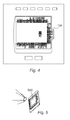
- FIG. 4 shows a more detailed schematic of the wire bonding for the chosen processor. This is a typical bonding arrangement and will vary according to the processor die used and on specific configurations requirements. However, it can be clearly seen that the notch 104 includes several rows of bond wires and therefore provides some additional capacity for bonding wires and other attachments. It is also feasible that Surface Mound Devices (SMD) could be positioned inside the cavity or inside the notch if the cavity depth is made greater than the height of the chosen SMD components.
- SMD Surface Mound Devices
- an imager die 500 is attached above the cavity (not shown) resting on a lip (not shown) surrounding the cavity.
- the imager includes an imager array made up of a plurality of pixels and may for example be an S952 or any other appropriate type.
- the imager array may be referred herein as an imaging module.
- the imager die may be rotated horizontally through 180° compared to traditional methods. This enables a better fit for subsequent actuators to the substrate. If this rotation occurs the image is then flipped onchip to correct for the effects of this placement by means of an onchip connection module or method.
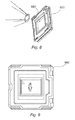
- Figure 6 shows wire bonding 600 for the imager die which again will vary depending on the imager die used and specific configurations requirements.
- Figure 7 shows the glue pattern 700 to permit the attachment of an Infra-Red (IR) glass holder that will completely protect the imager die from dust ingress which may contaminate the image array.
- the glue is a non-conductive glue containing spacer particles of approximately 30 ⁇ to ensure minimal tilt between the actuator and the substrate.
- the IR glass holder 800 is shown fitted above the substrate assembly with an aperture 802 centered over the image array. As previously indicated the IR glass holder prevents dust ingress and protects the delicate image array during later stages in the assembly of the camera module.
- the IR holder is effectively a universal interface for different actuator designs to be attached thereto. The attachment can be made for two or more than two contacts.
- the figure 9 is a diagram showing the glue pattern 900 for the lens or actuator attachment.
- the glue is a non-conductive glue and the glue pattern will be adjusted as necessary to suit the device.
- the lens or actuator assembly 1000 is then fitted over the top of the IR glass holder as shown in figure 10 .
- Two electrical contacts 1002 between the lens actuator assembly and the ceramic substrate are also shown.
- the notch 104 may take many different forms shapes and positions relative to the main cavity in the substrate.
- the build up of the different layers and components may also be varied in accordance with different requirements.
- the camera module is suitable for use in any appropriate device, such as a mobile telephone, other personal or communications devices or in a camera itself.
Landscapes
- Solid State Image Pick-Up Elements (AREA)
- Transforming Light Signals Into Electric Signals (AREA)
Abstract
Description
- The present invention relates to improvements in or relating to a modular camera system and a method of manufacturing the same.
- In the field of mobile communications the need for miniaturization and increased functionality and capability continues to grow. This has led to the desire to produce a functional camera system with an integrated image signal processor (ISP) in the camera module.
- Traditionally an integrated camera system has not been possible due to in compatibility between the imager and processor die sizes, power dissipation and substrate tracking density. In addition, combinations of image and processer have not been possible due to tracking and bonding requirements and constraints imposed by existing volume manufacturing capabilities.
- It is an object of the present invention to overcome at least some of the problems associated with the prior art.
- It is a further object of the present invention to produce a modular camera system with an integrated ISP
- The present invention provides a method and system as set out in the accompanying claims.
- According to one aspect of the present invention there is provided a camera module comprising a substrate including a cavity therein; a processor located in the cavity, one or more connections for connecting the processor to the substrate; an imaging module adapted to overlay the processor in the cavity and rest on at least part of the edge of the cavity; and one or more connections for connecting the imaging module to the substrate and the processor wherein the cavity includes a longitudinal cutout section adapted to accommodate at least one or more of the one or more connections for connecting the processor to the substrate or to accommodate one or more associated surface mounted components.
- The present invention offers a number of benefits. The present invention allows maximum leverage of existing 3Mpix/5Mpix camera module designs. A high the level of functional integration is achieved. The design supports all features of the processor as a stand-alone device. A single package solution is achieved which does not require a host system ISP. Imager/ISP integration is achieved in a single module. A complete solution is provided which can be tuned to optimize performance for the specific image/processor combination. The overall X/Y dimensions are smaller than that of a single die combining the imager and processor. A better isolation for noise and EMC purposes and an improved thermal performance is achieved. Application base-band processors can transfer more of the workload to the camera system. Flash and Shutter control can be achieved as an integrated capability thereby improving timing issues. There is an improved signaling environment between the imager and processor. Multiple image formats and images sizes are supported. An AF85 package size is achieved with a module height of less than 6mm with a standard Voice Coil Motor (VCM) actuator. The architecture is completely adaptable to implement support for other actuator technologies. There is no increase in package dimensions over existing standard imager-only modules. It is possible to support at least one secondary camera module.
- Reference will now be made, by way of example, to the accompanying drawings, in which:
-
Figure 1 is a diagram of a substrate of a camera module, in accordance with an embodiment of the invention, given by way of example, -
Figure 2 is a diagram of the next stage of manufacture of thefigure 1 module, in accordance with an embodiment of the invention, given by way of example, -
Figure 3 is a diagram of the next stage of manufacture of thefigure 1 module, in accordance with an embodiment of the invention, given by way of example -
Figure 4 is a diagram showing wire bonding for the module, in accordance with an embodiment of the invention, given by way of example, -
Figure 5 is a diagram of the next stage of manufacture of thefigure 1 module, in accordance with an embodiment of the invention, given by way of example, -
Figure 6 is a diagram of the next stage of manufacture of thefigure 1 module, in accordance with an embodiment of the invention, given by way of example, -
Figure 7 is a diagram showing the glue pattern for an IR holder of the module, in accordance with an embodiment of the invention, given by way of example, -
Figure 8 is a diagram showing the attachment of the IR holder, in accordance with an embodiment of the invention, given by way of example, -
Figure 9 is a diagram of a glue pattern for lens or actuator attachment in accordance with an embodiment of the invention, given by way of example, -
Figure 10 is a diagram of the final camera module, in accordance with an embodiment of the invention, given by way of example. - The present invention relates to a multichip modular camera based on stacking die and cavity substrates and making variations which permit a viable cavity bonding arrangement to support the functional combination of an imager and processor in a single package.
- The following description and associated drawings describe the assembly of the module in stages focusing on the multichip ceramic cavity approach implemented within the design.
-
Figure 1 shows a metalized ceramic module (MCM)ceramic substrate 100. The substrate includes acavity 102 which is shaped to include a notch orcutout section 104. The notch has to be relatively narrow to avoid unnecessary stresses being placed on the substrate during reliability tests. A typical width of the notch is in the region of 1.5mm. The cavity along with the notch is punched out of the substrate by means of an appropriately shaped punch tool, after which the substrate is fired before the next steps are carried out. The cavity is approximately 0.26 mm deep and shaped to offer a maximum support to the upper die whilst permitting maximum bonding height for the lower die. Thenotch 104 is particularly important in optimizing the support for the upper die and bonding from the lower die, as will be seen in greater detail below. The particular ceramic material is selected for rigidity and flatness. Typical materials may include High or Low Temperature Co-fired Ceramics (HTCC/LTCC). These types of material are easier to machine in order to produce the cavity, as there tends to be less shredding of particles which might lead to unacceptable levels of contamination. The use of ceramic material also helps in dissipating heat from the module and prevents hotspots arising that might interfere with satisfactory performance of the image array. In addition, ceramic substrates do not require the solder masks typical of organic substrates which would be difficult to apply to a cavity design. - The
cutout section 104 is located on an edge of the cavity along some, but not all, of its length. The notch extends longitudinally along the edge in question. There may be more than one notch on one edge or notches on more than one of the edges. - Certain surface mounted devices (SMD) 106 are mounted on the substrate. The SMD components have been selected for their physical size and placed so that their placement complements with the placement and arrangement of the imager die and the actuator to ensure that the image array centre is coincident with the package centre.
-
Figure 2 shows the introduction of aprocessor 200 into the cavity. An example of an appropriate processor is an image signal processor such as a V0986 processor. The die is backlapped to approximately 105 µ thickness and bonded using an appropriate mechanism, such as glue or a die attach film. The exact position of the processor is determined by reference to the position of the imager die, in order to maintain optical concentricity and meet bonding requirements for the processor die. There is sufficient space within the cavity for surface mounted devices associated with the processor die particularly due to the fact that the notch provides additional available space. Any wire bonding at this stage is minimised in terms of height to keep the module height to the minimum. The wire bonding is shown as 300 infigure 3 . It should be noted that the term wirebonding is used herein to cover any method or means of connection between different components, devices and substrates. Other examples of connections may include Through Silicon Vias (TSVs) or any other appropriate connection. -
Figure 4 shows a more detailed schematic of the wire bonding for the chosen processor. This is a typical bonding arrangement and will vary according to the processor die used and on specific configurations requirements. However, it can be clearly seen that thenotch 104 includes several rows of bond wires and therefore provides some additional capacity for bonding wires and other attachments. It is also feasible that Surface Mound Devices (SMD) could be positioned inside the cavity or inside the notch if the cavity depth is made greater than the height of the chosen SMD components. - Referring to
figure 5 animager die 500 is attached above the cavity (not shown) resting on a lip (not shown) surrounding the cavity. The imager includes an imager array made up of a plurality of pixels and may for example be an S952 or any other appropriate type. The imager array may be referred herein as an imaging module. The imager die may be rotated horizontally through 180° compared to traditional methods. This enables a better fit for subsequent actuators to the substrate. If this rotation occurs the image is then flipped onchip to correct for the effects of this placement by means of an onchip connection module or method.Figure 6 showswire bonding 600 for the imager die which again will vary depending on the imager die used and specific configurations requirements. - Referring to
figure 7 the subsequent manufacturing step for the module will now be described in greater detail.Figure 7 shows theglue pattern 700 to permit the attachment of an Infra-Red (IR) glass holder that will completely protect the imager die from dust ingress which may contaminate the image array. The glue is a non-conductive glue containing spacer particles of approximately 30 µ to ensure minimal tilt between the actuator and the substrate. - Referring to
figure 8 theIR glass holder 800 is shown fitted above the substrate assembly with anaperture 802 centered over the image array. As previously indicated the IR glass holder prevents dust ingress and protects the delicate image array during later stages in the assembly of the camera module. The IR holder is effectively a universal interface for different actuator designs to be attached thereto. The attachment can be made for two or more than two contacts. - The
figure 9 is a diagram showing theglue pattern 900 for the lens or actuator attachment. The glue is a non-conductive glue and the glue pattern will be adjusted as necessary to suit the device. The lens oractuator assembly 1000 is then fitted over the top of the IR glass holder as shown infigure 10 . Twoelectrical contacts 1002 between the lens actuator assembly and the ceramic substrate are also shown. - It will be appreciated that a number of variations can be made to the present invention, for example, different materials and layouts of components. The
notch 104 may take many different forms shapes and positions relative to the main cavity in the substrate. - The build up of the different layers and components may also be varied in accordance with different requirements.
- The camera module is suitable for use in any appropriate device, such as a mobile telephone, other personal or communications devices or in a camera itself.
Claims (16)
- A camera module comprising a substrate including a cavity therein; a processor located in the cavity, one or more connections for connecting the processor to the substrate; an imaging module adapted to overlay the processor in the cavity and rest on at least part of the edge of the cavity; and one or more connections for connecting the imaging module to the substrate and the processor wherein the cavity includes a longitudinal cutout section adapted to accommodate at least one or more of the one or more connections for connecting the processor to the substrate or to accommodate one or more associated surface mounted components.
- The camera module of claim 1, wherein the one or more connections comprise wire bonding.
- The camera module of claim 1 or claim 2, wherein the longitudinal cutout section can accommodate one or more connections and one or more surface mounted components.
- The camera module of any preceding claims, wherein the longitudinal cutout section extends along a part of an edge of the cavity.
- The camera module of claim 4, wherein more than one longitudinal cutout section extends along a part of an edge of the cavity.
- The camera module of claim 4 or 5, wherein more than one longitudinal cutout sections extend along a part of different edges.
- The camera module of any preceding claim, wherein the substrate is a ceramics material.
- The camera module of any preceding claim, wherein the processor is an image signal processor.
- The camera module of any preceding claim, wherein the imaging module includes an imager array.
- The camera module of any preceding claim further comprising an onchip connection, wherein the imager array is positioned relative to the substrate to minimize the overall space the image array occupies.
- The camera module of claim 10, further including a correction circuit for correcting for the position of the image array.
- The camera module of any preceding claim, wherein the longitudinal cutout section has one edge substantially longer that the other edge.
- The camera module of claim 12, wherein the edges are straight.
- The camera module of any preceding claim, for use in a device.
- A computer device, including a camera module according to any of claims 1 to 13.
- A mobile telephone including a camera module according to any of claims 1 to 13.
Applications Claiming Priority (1)
| Application Number | Priority Date | Filing Date | Title |
|---|---|---|---|
| GBGB0911171.7A GB0911171D0 (en) | 2009-06-29 | 2009-06-29 | Improvements in or relating to a modular camera system and a method of manufacturing the same |
Publications (2)
| Publication Number | Publication Date |
|---|---|
| EP2270860A2 true EP2270860A2 (en) | 2011-01-05 |
| EP2270860A3 EP2270860A3 (en) | 2013-04-17 |
Family
ID=41008389
Family Applications (1)
| Application Number | Title | Priority Date | Filing Date |
|---|---|---|---|
| EP10167466.1A Withdrawn EP2270860A3 (en) | 2009-06-29 | 2010-06-28 | Improvements in or relating to a modular camera system and a method of manufacturing the same |
Country Status (3)
| Country | Link |
|---|---|
| US (1) | US8488056B2 (en) |
| EP (1) | EP2270860A3 (en) |
| GB (1) | GB0911171D0 (en) |
Families Citing this family (2)
| Publication number | Priority date | Publication date | Assignee | Title |
|---|---|---|---|---|
| JP2019507996A (en) | 2015-12-14 | 2019-03-22 | レッド.コム,エルエルシー | Modular digital camera and mobile phone |
| US11581351B2 (en) * | 2019-07-25 | 2023-02-14 | Apple Inc. | Hybrid sensor shift platform |
Family Cites Families (6)
| Publication number | Priority date | Publication date | Assignee | Title |
|---|---|---|---|---|
| US4630172A (en) * | 1983-03-09 | 1986-12-16 | Printed Circuits International | Semiconductor chip carrier package with a heat sink |
| US6627983B2 (en) | 2001-01-24 | 2003-09-30 | Hsiu Wen Tu | Stacked package structure of image sensor |
| JP4641820B2 (en) | 2005-02-17 | 2011-03-02 | 三洋電機株式会社 | Manufacturing method of semiconductor device |
| JP2006237134A (en) | 2005-02-23 | 2006-09-07 | Sharp Corp | Solid-state imaging device |
| US20060219862A1 (en) | 2005-03-31 | 2006-10-05 | Kai-Kuang Ho | Compact camera module with reduced thickness |
| CN100531310C (en) * | 2006-01-14 | 2009-08-19 | 鸿富锦精密工业(深圳)有限公司 | Digital camera module |
-
2009
- 2009-06-29 GB GBGB0911171.7A patent/GB0911171D0/en not_active Ceased
-
2010
- 2010-06-28 US US12/824,760 patent/US8488056B2/en not_active Expired - Fee Related
- 2010-06-28 EP EP10167466.1A patent/EP2270860A3/en not_active Withdrawn
Non-Patent Citations (1)
| Title |
|---|
| None |
Also Published As
| Publication number | Publication date |
|---|---|
| GB0911171D0 (en) | 2009-08-12 |
| EP2270860A3 (en) | 2013-04-17 |
| US20100328526A1 (en) | 2010-12-30 |
| US8488056B2 (en) | 2013-07-16 |
Similar Documents
| Publication | Publication Date | Title |
|---|---|---|
| TWI479645B (en) | Method of manufacturing solid-state imaging element, solid-state imaging element and electronic device | |
| EP2341541A2 (en) | Image sensor packaging structure with predetermined focal length | |
| CN102761697B (en) | Based on camera module and the manufacture method thereof of wafer | |
| US8981511B2 (en) | Multi-chip package for imaging systems | |
| US8902356B2 (en) | Image sensor module having image sensor package | |
| US8110884B2 (en) | Methods of packaging imager devices and optics modules, and resulting assemblies | |
| US20190267416A1 (en) | Image sensor mounting base, imaging device, and imaging module | |
| US10446598B2 (en) | Semiconductor device, manufacturing method, and electronic apparatus | |
| CN102386192B (en) | Method of manufacturing optical sensor, optical sensor, and camera including optical sensor | |
| EP2388821A1 (en) | Manufacturing method and structure for wafer level image sensor module with fixed focal length | |
| CN1176556A (en) | Imaging device and manufacturing method thereof | |
| JP7449920B2 (en) | semiconductor equipment | |
| CN108391451B (en) | Image pickup element package, method of manufacturing the same, and image pickup apparatus | |
| CN112020771A (en) | Substrate for mounting electronic component, electronic device, and electronic module | |
| KR20200063102A (en) | Filming assembly and its packaging method, lens module, electronic device | |
| WO2016052217A1 (en) | Semiconductor package, sensor module, and manufacturing method | |
| CN105489620A (en) | Method for manufacturing solid-state imaging device and method for manufacturing camera module | |
| CN109155288A (en) | Electronic component mounting substrates and electronic devices | |
| US8488056B2 (en) | Modular camera system and a method of manufacturing the same | |
| JP2018117344A (en) | 3D photoelectric imaging module | |
| CN104603946B (en) | Shooting unit, shooting device, and method of manufacturing the shooting unit | |
| EP2575176B1 (en) | Folded tape package for electronic devices | |
| WO2022135256A1 (en) | Camera module and electronic device | |
| JP6990317B2 (en) | Imaging unit and imaging device | |
| US8584337B2 (en) | Electronic component repair method |
Legal Events
| Date | Code | Title | Description |
|---|---|---|---|
| PUAI | Public reference made under article 153(3) epc to a published international application that has entered the european phase |
Free format text: ORIGINAL CODE: 0009012 |
|
| AK | Designated contracting states |
Kind code of ref document: A2 Designated state(s): AL AT BE BG CH CY CZ DE DK EE ES FI FR GB GR HR HU IE IS IT LI LT LU LV MC MK MT NL NO PL PT RO SE SI SK SM TR |
|
| AX | Request for extension of the european patent |
Extension state: BA ME RS |
|
| PUAL | Search report despatched |
Free format text: ORIGINAL CODE: 0009013 |
|
| AK | Designated contracting states |
Kind code of ref document: A3 Designated state(s): AL AT BE BG CH CY CZ DE DK EE ES FI FR GB GR HR HU IE IS IT LI LT LU LV MC MK MT NL NO PL PT RO SE SI SK SM TR |
|
| AX | Request for extension of the european patent |
Extension state: BA ME RS |
|
| RIC1 | Information provided on ipc code assigned before grant |
Ipc: H01L 27/146 20060101AFI20130312BHEP |
|
| 17P | Request for examination filed |
Effective date: 20131017 |
|
| RBV | Designated contracting states (corrected) |
Designated state(s): AL AT BE BG CH CY CZ DE DK EE ES FI FR GB GR HR HU IE IS IT LI LT LU LV MC MK MT NL NO PL PT RO SE SI SK SM TR |
|
| 17Q | First examination report despatched |
Effective date: 20140203 |
|
| STAA | Information on the status of an ep patent application or granted ep patent |
Free format text: STATUS: THE APPLICATION IS DEEMED TO BE WITHDRAWN |
|
| 18D | Application deemed to be withdrawn |
Effective date: 20140614 |